EP3734542A1 - Image acquisition device, and display device equipped with same - Google Patents
Image acquisition device, and display device equipped with same Download PDFInfo
- Publication number
- EP3734542A1 EP3734542A1 EP18897291.3A EP18897291A EP3734542A1 EP 3734542 A1 EP3734542 A1 EP 3734542A1 EP 18897291 A EP18897291 A EP 18897291A EP 3734542 A1 EP3734542 A1 EP 3734542A1
- Authority
- EP
- European Patent Office
- Prior art keywords
- light
- signal
- pass filter
- modulation signal
- image acquiring
- Prior art date
- Legal status (The legal status is an assumption and is not a legal conclusion. Google has not performed a legal analysis and makes no representation as to the accuracy of the status listed.)
- Withdrawn
Links
Images
Classifications
-
- H—ELECTRICITY
- H10—SEMICONDUCTOR DEVICES; ELECTRIC SOLID-STATE DEVICES NOT OTHERWISE PROVIDED FOR
- H10F—INORGANIC SEMICONDUCTOR DEVICES SENSITIVE TO INFRARED RADIATION, LIGHT, ELECTROMAGNETIC RADIATION OF SHORTER WAVELENGTH OR CORPUSCULAR RADIATION
- H10F39/00—Integrated devices, or assemblies of multiple devices, comprising at least one element covered by group H10F30/00, e.g. radiation detectors comprising photodiode arrays
- H10F39/80—Constructional details of image sensors
- H10F39/806—Optical elements or arrangements associated with the image sensors
-
- G—PHYSICS
- G06—COMPUTING OR CALCULATING; COUNTING
- G06V—IMAGE OR VIDEO RECOGNITION OR UNDERSTANDING
- G06V10/00—Arrangements for image or video recognition or understanding
- G06V10/10—Image acquisition
- G06V10/12—Details of acquisition arrangements; Constructional details thereof
- G06V10/14—Optical characteristics of the device performing the acquisition or on the illumination arrangements
- G06V10/141—Control of illumination
-
- G—PHYSICS
- G06—COMPUTING OR CALCULATING; COUNTING
- G06V—IMAGE OR VIDEO RECOGNITION OR UNDERSTANDING
- G06V10/00—Arrangements for image or video recognition or understanding
- G06V10/10—Image acquisition
- G06V10/12—Details of acquisition arrangements; Constructional details thereof
- G06V10/14—Optical characteristics of the device performing the acquisition or on the illumination arrangements
- G06V10/147—Details of sensors, e.g. sensor lenses
-
- G—PHYSICS
- G06—COMPUTING OR CALCULATING; COUNTING
- G06V—IMAGE OR VIDEO RECOGNITION OR UNDERSTANDING
- G06V40/00—Recognition of biometric, human-related or animal-related patterns in image or video data
- G06V40/10—Human or animal bodies, e.g. vehicle occupants or pedestrians; Body parts, e.g. hands
- G06V40/12—Fingerprints or palmprints
- G06V40/13—Sensors therefor
- G06V40/1318—Sensors therefor using electro-optical elements or layers, e.g. electroluminescent sensing
-
- H—ELECTRICITY
- H04—ELECTRIC COMMUNICATION TECHNIQUE
- H04N—PICTORIAL COMMUNICATION, e.g. TELEVISION
- H04N23/00—Cameras or camera modules comprising electronic image sensors; Control thereof
- H04N23/70—Circuitry for compensating brightness variation in the scene
- H04N23/72—Combination of two or more compensation controls
-
- H—ELECTRICITY
- H10—SEMICONDUCTOR DEVICES; ELECTRIC SOLID-STATE DEVICES NOT OTHERWISE PROVIDED FOR
- H10F—INORGANIC SEMICONDUCTOR DEVICES SENSITIVE TO INFRARED RADIATION, LIGHT, ELECTROMAGNETIC RADIATION OF SHORTER WAVELENGTH OR CORPUSCULAR RADIATION
- H10F39/00—Integrated devices, or assemblies of multiple devices, comprising at least one element covered by group H10F30/00, e.g. radiation detectors comprising photodiode arrays
- H10F39/80—Constructional details of image sensors
- H10F39/803—Pixels having integrated switching, control, storage or amplification elements
Definitions
- the present invention relates to an image acquiring apparatus capable of acquiring a fingerprint or the like of a person, and a display apparatus equipped therewith.
- PTL 1 to PTL 6 and the like disclose a liquid crystal display and an organic EL display in which a fingerprint sensor using a photosensor is integrated.
- An object of the present invention is to provide an image acquiring apparatus capable of imaging an object even outdoors, and a display apparatus equipped therewith.
- An image acquiring apparatus includes: a light irradiation unit configured to be capable of radiating light modulated with a modulation signal in a predetermined frequency band; photosensors configured to be capable of receiving the light radiated from the light irradiation unit, the light including reflected light reflected by an object, and the photosensors being arranged in a matrix; and a generation unit configured to generate a DC component from an electrical signal output from the photosensor due to the light received by the photosensor on the basis of the predetermined frequency band or the modulation signal.
- the light irradiation unit may include a light source; a brightness instruction value generation unit configured to generate a brightness instruction value for the light source; and a modulation signal generation unit configured to generate a modulation signal for modulating the brightness instruction value with the predetermined frequency band.
- the generation unit may include a band pass filter configured to cut off a DC component caused by external light in the electrical signal; and a low pass filter configured to pass the DC component from a signal obtained by multiplying the electrical signal that has passed through the band pass filter by the modulation signal synchronized with the electrical signal, with a frequency lower than the predetermined frequency band being a cutoff frequency.
- the generation unit may include a band pass filter in which the predetermined frequency band is included in a pass band of the electrical signal; and a low pass filter configured to pass the DC component from a signal based on the electrical signal that has passed through the band pass filter, with a frequency lower than the predetermined frequency band being a cutoff frequency.
- the generation unit may include a low pass filter configured to pass the DC component from a signal obtained by multiplying the electrical signal output from the photosensor by the modulation signal synchronized with the electrical signal, with a frequency lower than the predetermined frequency band being a cutoff frequency.
- a display apparatus includes the above image acquiring apparatus.
- an image acquiring apparatus capable of imaging an object even outdoors, and a display apparatus equipped therewith can be provided.
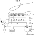
- Fig. 1 is a schematic diagram of an image acquiring apparatus 1 according to a first embodiment of the present invention.
- the image acquiring apparatus 1 illustrated in Fig. 1 is an apparatus for acquiring an image (moving image) of an object such as a fingerprint.
- the image acquiring apparatus 1 includes a sensor unit 10, a brightness instruction value generation unit 2, a modulation signal generation unit 3, a DA converter 4, a current source 5, a band pass filter 7, an amplifier 8, an AD converter 9, and a signal comparison unit 20.
- the sensor unit 10 includes a glass substrate 11, a photosensor 12, a protective insulating film 13, a cover glass 14, and a backlight 15.
- the glass substrate 11 is a transparent substrate, and an array of photosensors 12 arranged in a matrix in portion or all of a sensor front surface is formed on a front surface side of the glass substrate 11.
- measurement may be performed over all or a part of the array of photosensors 12 by parallelizing a plurality of measurement circuits or switching between the photosensors 12 for measurement using a switch element (not illustrated) to perform the measurement.
- Each photosensor 12 is a photoelectric conversion element in which a semiconductor film is used as a light reception portion, and outputs a voltage signal (electrical signal) according to the intensity of incident light. Reflected light that is radiated from a light irradiation unit, reflected by a finger FG, and travels from a front surface side to an opposite non-front surface side of the device, and/or external light such as sunlight is incident on each photosensor 12.
- the photosensor 12 is, for example, a thin film transistor (TFT) having a well-known double gate structure, or an LED.
- TFT thin film transistor
- the photosensor 12 is covered with the protective insulating film 13.
- the protective insulating film 13 has a function of protecting an interface of the semiconductor film of the photosensor 12, has an insulating property and transparent to light, and is formed of, for example, silicon nitride or silicon oxide.
- the cover glass 14 is provided on the protective insulating film 13.
- a fingerprint image moving image
- the backlight 15 serving as a light source is provided below the glass substrate 11.
- a well-known backlight is adopted as the backlight 15, and for example, the backlight 15 is configured of a plurality of LEDs 16.
- Light L from the backlight 15 is reflected by the finger FG placed on the cover glass 14, and reflected light thereof is incident on each photosensor 12.
- the brightness instruction value generation unit 2 generates and outputs a brightness instruction value (current value) for radiating light with a desired brightness from the backlight 15.
- the modulation signal generation unit 3 generates and outputs a modulation signal in a predetermined frequency band, such as a sine wave modulation signal at a predetermined frequency.
- the modulation signal may be any other signal including a frequency band convenient for modulation and having an average value of zero, such as pseudo random noise or a pseudo white binary signal.
- the frequency band may be a frequency band which is low such that responses of the current source 5, the photosensor 12, and the backlight 15 catch up with and which is high such that flickering of the LED 16 is not noticeable.
- a response speed thereof is substantially determined by a mobility ⁇ e of the TFT and can be a maximum of about 10 MHz.
- a noise component decreases as the frequency increases, selection of a higher frequency can result in a decrease in an S/N ratio or a size of a filter.
- a frequency band of the modulation signal is, for example, 1 to 5 kHz.
- the brightness instruction value generated by the brightness instruction value generation unit 2 is modulated by a modulation signal and input to the DA converter 4 as a modulation instruction value. Further, the modulation signal generated by the modulation signal generation unit 3 is also output to a delay unit 21 of the signal comparison unit 20 to be described below.
- the DA converter 4 converts the brightness instruction value input as a digital signal to an analog signal, and outputs the analog signal to a current instruction value input of the current source 5.
- the current source 5 changes a current from a power supply 6 to a current value according to the modulation instruction value, and outputs the current value to the backlight 15.
- a current source 6 changes a current from a power supply 6 to a current value according to the modulation instruction value, and outputs the current value to the backlight 15.
- an LED driver IC using a switching power supply or an active matrix type LED drive circuit is used as the current source 5.
- the band pass filter 7 is a filter that mainly passes only a specific frequency component of the voltage signal output from the photosensor 12. Since the voltage signal output from the photosensor 12 due to external light is mostly DC or low frequency components close to DC, an unnecessary DC component and low frequency component are cut off in the measurement. Thereby, it is possible to effectively use a measurement range in the AD converter 9 to be described below for measurement of a modulation component, and to improve an S/N ratio.
- the amplifier 8 amplifies the voltage signal that has passed through the band pass filter 7.
- the AD converter 9 converts the voltage signal amplified as an analog signal into a digital signal.
- the signal comparison unit 20 includes the delay unit 21 and a low pass filter 22.
- the delay unit 21 delays the modulation signal from the modulation signal generation unit 3. This is because there is a time difference between a timing at which the modulation signal output from the modulation signal generation unit 3 to the DA converter 4 is reflected by the finger FG and then is incident on the signal comparison unit 20 and a timing at which the modulation signal from the modulation signal generation unit 3 is directly input to the signal comparison unit 20.
- the modulation signal is delayed by a clocks for correction of the time difference. That is, the modulation signal from the modulation signal generation unit 3 is synchronized with the voltage signal from the photosensor 12.
- the low pass filter 22 passes a signal at a frequency lower than the frequency band of the modulation signal in a signal obtained by multiplying the delayed modulation signal by the amplified voltage signal, with a frequency lower than the frequency band of the modulation signal being a cutoff frequency, and outputs the signal as an output signal (image signal).
- an AC component in a signal obtained by multiplying the voltage signal output from the photosensor 12 due to the reflected light from the finger FG by the modulation signal is removed by the low pass filter 22, and a low frequency component around a DC is output as an output signal (image signal).
- the cutoff frequency is determined on the basis of a frequency band of an entire fingerprint sensor system including the image acquiring apparatus 1, the finger FG, and the like.
- the low pass filter 22 is, for example, a FIR filter, an IIR filter, or a combination thereof.
- the low pass filter 22 may be implemented as a filter that integrates a signal for a time that is an integral multiple of a time of a repetition period of the modulation signal.
- This filter can also be regarded as a low pass filter with a frequency lower than the frequency band of the modulation signal being a cutoff frequency, but is a filter capable of reliably removing the frequency component of the modulation signal while widening a pass band of the low pass filter 22.
- An image (moving image) of a fingerprint of the finger is created in a control unit (not illustrated) on the basis of the output signal output from the low pass filter 22.
- the light irradiation unit capable of radiating the light modulated with the modulation signal at a predetermined frequency is included, and a DC component is generated from the voltage signal output from the photosensor 12 due to the light received by the photosensor 12 on the basis of a predetermined frequency band or the modulation signal.
- the image acquiring apparatus 1 includes the band pass filter 7 that cuts off a DC component caused by external light in the voltage signal, and the low pass filter 22 that passes a DC component in a signal obtained by multiplying the voltage signal that has passed through the band pass filter 7 by the modulation signal synchronized with the voltage signal, with a frequency lower than the frequency band being a cutoff frequency.
- the light irradiation unit includes the backlight 15, a brightness instruction value generation unit 2 that generates the brightness instruction value for the backlight 15, and the modulation signal generation unit 3 that generates the modulation signal for modulating the brightness instruction value with a predetermined frequency.
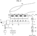
- Fig. 2 is a schematic diagram of an image acquiring apparatus 101 according to a second embodiment of the present invention.
- the same components as those in the first embodiment are denoted by the same reference signs.
- An absolute value unit 23 and a low pass filter 24 are included in place of the signal comparison unit 20 of the first embodiment, as illustrated in Fig. 2 .
- the predetermined frequency generated by the modulation signal generation unit 3 in the second embodiment is determined on the basis of the entire sensor system including the image acquiring apparatus 101, the finger FG, and the like, as in the first embodiment.
- the predetermined frequency is determined to be low such that the responses of the current source 5 and the backlight 15 catch up with and flickering of the LED 16 is not noticeable.
- the modulation signal is, for example, a sine wave, the modulation signal may be a rectangular wave or a triangular wave.
- the band pass filter 7 in the second embodiment is a filter in which a narrow range including a frequency of the modulation signal generated by the modulation signal generation unit 3 is a pass band.
- a range of the pass band is determined on the basis of the frequency band of the entire sensor system including the image acquiring apparatus 101, the finger FG, and the like.
- the absolute value unit 23 converts a negative component of the voltage signal from the AD converter 9 to a positive component. That is, the absolute value unit 23 obtains an absolute value of an amplitude of the voltage signal. This is preprocessing for processing the voltage signal in the next low pass filter 24. Although a process in the absolute value unit 23 is digital processing in the second embodiment, a bridge rectifier circuit may be used when analog processing is performed.
- the low pass filter 24 passes a signal at a frequency lower than the frequency of the modulation signal in the voltage signal subjected to absolute value processing in the absolute value unit 23, with the frequency lower than a frequency band of the modulation signal being a cutoff frequency, and outputs the signal as an output signal.
- an AC component of the voltage signal output from the photosensor 12 due to the reflected light from the finger FG is removed by the low pass filter 24, and a component around the DC is output as an output signal (color image signal).
- the cutoff frequency (the range of the pass band) is determined on the basis of the frequency band of the entire sensor system including the image acquiring apparatus 101, the finger FG, and the like.
- a control unit (not illustrated) creates an image (moving image) of a fingerprint of the finger on the basis of the output signal output from the low pass filter 24.
- the image acquiring apparatus 101 includes the band pass filter 7 in which a frequency band is a pass band of the electrical signal, and the low pass filter 24 that passes a DC component in a signal based on the voltage signal that has passed through the band pass filter 7, with a frequency lower than the frequency band being a cutoff frequency.
- the band pass filter 7 in which a frequency band is a pass band of the electrical signal
- the low pass filter 24 that passes a DC component in a signal based on the voltage signal that has passed through the band pass filter 7, with a frequency lower than the frequency band being a cutoff frequency.
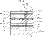
- Fig. 3 is a cross-sectional view in which a portion of the display apparatus 201 is cut off.
- the display apparatus 201 is a thin film transistor (TFT) type active matrix liquid crystal display. Since a configuration of the active matrix liquid crystal display is known, detailed description of the known configuration will be omitted in the following description.
- TFT thin film transistor
- B1 indicates a display surface side
- B2 indicates a non-display surface side opposite to the display surface side.
- illustration of components other than the sensor unit 10 is omitted.
- the glass substrates 30, 11, and 40 are provided as transparent substrates in that order from the display surface side B1 to the non-display surface side B2, as illustrated in Fig. 3 .
- a plastic substrate such as polycarbonate can be adopted in place of the glass substrate.
- a polarizing element PL is provided on the display surface side B1 of the glass substrate 30, and a transparent cover glass 14 is provided on the polarizing element PL.
- a color filter 50 is provided on the non-display surface side B2 of the glass substrate 30 as a filter that selectively transmits light with a predetermined color.
- the color filter 50 includes a light-shielding black matrix BM formed in a lattice form on the front surface of the glass substrate 30 in correspondence with each pixel of a screen, and three colored portions (R, G, B) that transmit light with a predetermined color.
- a material of the black matrix BM a metal chromium film can be adopted for reasons such as a light-shielding property, ease of manufacture, and corrosion resistance.
- the three colored portions (R, G, B) are formed of a known resist material, and are, for example, an organic resin material containing a pigment.
- Switching elements TR each made of a thin film transistor (TFT) are formed in a matrix form in correspondence with each pixel on the display surface side B1 of a glass substrate 40, and a pixel electrode EL2 is formed in a matrix form on the switching element TR via a protective insulating film 80.
- TFT thin film transistor
- LTPS low-temperature poly-Si
- amorphous Si type is adopted as the TFT.
- a common electrode EL1 facing the pixel electrode EL2 is formed on the non-display surface side B2 of the glass substrate 11.
- the common electrode EL1 and the pixel electrode EL2 are formed of a transparent conductive film such as indium tin oxide (ITO).
- a well-known liquid crystal material LC is filled between the common electrode EL1 and the pixel electrode EL2.
- the polarizing element PL is provided on the non-display surface B2 side of the glass substrate 40, and the backlight 15 serving as a light source is provided on the polarizing element PL.
- a well-known backlight is adopted as the backlight 15.
- the array of photosensors 12 arranged in a matrix form on a portion of a screen of the display apparatus is formed on the display surface side B1 of the glass substrate 11.
- a single photosensor 12 is provided for each pixel, but the present invention is not limited thereto and a plurality of photosensors 12 can also be provided for one pixel.
- the protective insulating film 13 covers the photosensor 12.
- the light L from the backlight 15 is reflected by a finger FG placed on the cover glass 14, and the reflected light passes through the three colored portions (R, G, B) of the color filter 50 and is incident on each of the photosensors 12, as illustrated in Fig. 3 . Thereby, it is possible to capture a color image of the fingerprint.
- the respective layers are formed on the glass substrates 30, 11, and 40 by appropriately performing a film forming process such as a well-known PVD method or CVD method, a mask process such as a photolithography method, and a thin film shape processing process such as an etching method.
- a film forming process such as a well-known PVD method or CVD method
- a mask process such as a photolithography method
- a thin film shape processing process such as an etching method.
- the glass substrate 30 and the glass substrate 11 are then bonded to each other using an adhesive such as an ultraviolet curing resin, with the color filter 50 and the photosensor 12 facing each other.
- the display apparatus 201 is manufactured through steps such as bonding the glass substrate 40 thereto and injecting a liquid crystal material LC.
- the display apparatus 201 it is possible to provide a display apparatus 201 including the image acquiring apparatus 1 or 101 capable of imaging an object even outdoors.
- Embodiments are not limited to the above-described embodiments. A person skilled in the art can perform various additions or changes without departing from the scope of the present invention.
- the image acquiring apparatus 1 may not include the band pass filter 7.
- the signal comparison unit 20 can cut off the DC component caused by the external light from the voltage signal detected by the photosensor 12 and obtain a voltage signal on which an influence of the external light has been curbed, without the band pass filter 7.
- the image acquisition of the image acquiring apparatus 1 or 101 described above is performed in both analog and digital manners, all the processes may be performed in an analog manner, all the processes may be performed in a digital manner, or the signal processing may be performed by software on a processor such as a digital signal processor.
- Each various filter is implemented as analog filter or digital filters depending on the form of the circuit.
- the absolute value unit 23 described above obtains the absolute value of the amplitude of the voltage signal in the image acquiring apparatus 101, the voltage signal may be squared.
- an IPS scheme, a VA scheme, or the like may be used in place of a TN scheme as a liquid crystal display scheme, or a passive matrix scheme or the like may be used in place of an active matrix scheme as a driving scheme.
- the display apparatus 201 is not limited to the liquid crystal display, but may be an organic EL display or a micro LED display. When the organic EL display is used as the display apparatus 201, an LED for a display itself can also serve as both the backlight 15 and the photosensor 12 and a simple structure can be achieved.
Landscapes
- Engineering & Computer Science (AREA)
- Multimedia (AREA)
- Physics & Mathematics (AREA)
- General Physics & Mathematics (AREA)
- Theoretical Computer Science (AREA)
- Human Computer Interaction (AREA)
- Vascular Medicine (AREA)
- Health & Medical Sciences (AREA)
- General Health & Medical Sciences (AREA)
- Signal Processing (AREA)
- Image Input (AREA)
- Measurement Of The Respiration, Hearing Ability, Form, And Blood Characteristics Of Living Organisms (AREA)
- Devices For Indicating Variable Information By Combining Individual Elements (AREA)
Abstract
Description
- The present invention relates to an image acquiring apparatus capable of acquiring a fingerprint or the like of a person, and a display apparatus equipped therewith.
-
PTL 1 toPTL 6 and the like disclose a liquid crystal display and an organic EL display in which a fingerprint sensor using a photosensor is integrated. -
- [PTL 1] Japanese Patent Application Publication No.
2003-287731 - [PTL 2] Japanese Patent Application Publication No.
2004-326806 - [PTL 3] Japanese Patent Application Publication No.
2006-503333 - [PTL 4] Japanese Patent Application Publication No.
2006-086333 - [PTL 5] Japanese Patent Application Publication No.
2002-245443 - [PTL 6] Japanese Patent Application Publication No.
2009-064071 - In the displays disclosed in
PTL 1 toPTL 6 and the like, excluding an influence of external light from sunlight is not considered, and it is difficult to capture a fingerprint image based on reflected light of a backlight outdoors. - An object of the present invention is to provide an image acquiring apparatus capable of imaging an object even outdoors, and a display apparatus equipped therewith.
- An image acquiring apparatus according to one embodiment of the present invention includes: a light irradiation unit configured to be capable of radiating light modulated with a modulation signal in a predetermined frequency band; photosensors configured to be capable of receiving the light radiated from the light irradiation unit, the light including reflected light reflected by an object, and the photosensors being arranged in a matrix; and a generation unit configured to generate a DC component from an electrical signal output from the photosensor due to the light received by the photosensor on the basis of the predetermined frequency band or the modulation signal.
- The light irradiation unit may include a light source; a brightness instruction value generation unit configured to generate a brightness instruction value for the light source; and a modulation signal generation unit configured to generate a modulation signal for modulating the brightness instruction value with the predetermined frequency band.
- The generation unit may include a band pass filter configured to cut off a DC component caused by external light in the electrical signal; and a low pass filter configured to pass the DC component from a signal obtained by multiplying the electrical signal that has passed through the band pass filter by the modulation signal synchronized with the electrical signal, with a frequency lower than the predetermined frequency band being a cutoff frequency.
- The generation unit may include a band pass filter in which the predetermined frequency band is included in a pass band of the electrical signal; and a low pass filter configured to pass the DC component from a signal based on the electrical signal that has passed through the band pass filter, with a frequency lower than the predetermined frequency band being a cutoff frequency.
- The generation unit may include a low pass filter configured to pass the DC component from a signal obtained by multiplying the electrical signal output from the photosensor by the modulation signal synchronized with the electrical signal, with a frequency lower than the predetermined frequency band being a cutoff frequency.
- A display apparatus according to one embodiment of the present invention includes the above image acquiring apparatus.
- According to the present invention, an image acquiring apparatus capable of imaging an object even outdoors, and a display apparatus equipped therewith can be provided.
-
- [
Fig. 1] Fig. 1 is a schematic diagram of an image acquiring apparatus according to a first embodiment. - [
Fig. 2] Fig. 2 is a schematic diagram of an image acquiring apparatus according to a second embodiment. - [
Fig. 3] Fig. 3 is a cross-sectional view of a portion of a display apparatus. - Hereinafter, embodiments of the present invention will be described with reference to the drawings.
-
Fig. 1 is a schematic diagram of animage acquiring apparatus 1 according to a first embodiment of the present invention. - The
image acquiring apparatus 1 illustrated inFig. 1 is an apparatus for acquiring an image (moving image) of an object such as a fingerprint. Theimage acquiring apparatus 1 includes asensor unit 10, a brightness instructionvalue generation unit 2, a modulationsignal generation unit 3, aDA converter 4, acurrent source 5, aband pass filter 7, anamplifier 8, anAD converter 9, and asignal comparison unit 20. - The
sensor unit 10 includes aglass substrate 11, aphotosensor 12, a protectiveinsulating film 13, acover glass 14, and abacklight 15. - The
glass substrate 11 is a transparent substrate, and an array ofphotosensors 12 arranged in a matrix in portion or all of a sensor front surface is formed on a front surface side of theglass substrate 11. Although a method of performing measurement with onephotosensor 12 will be described in the following description and drawings, measurement may be performed over all or a part of the array ofphotosensors 12 by parallelizing a plurality of measurement circuits or switching between thephotosensors 12 for measurement using a switch element (not illustrated) to perform the measurement. - Each
photosensor 12 is a photoelectric conversion element in which a semiconductor film is used as a light reception portion, and outputs a voltage signal (electrical signal) according to the intensity of incident light. Reflected light that is radiated from a light irradiation unit, reflected by a finger FG, and travels from a front surface side to an opposite non-front surface side of the device, and/or external light such as sunlight is incident on eachphotosensor 12. Thephotosensor 12 is, for example, a thin film transistor (TFT) having a well-known double gate structure, or an LED. - The
photosensor 12 is covered with the protectiveinsulating film 13. The protectiveinsulating film 13 has a function of protecting an interface of the semiconductor film of thephotosensor 12, has an insulating property and transparent to light, and is formed of, for example, silicon nitride or silicon oxide. - The
cover glass 14 is provided on the protectiveinsulating film 13. By a finger FG of a human body being brought into contact with a front surface of thecover glass 14, a fingerprint image (moving image) can be captured as will be described below. - The
backlight 15 serving as a light source is provided below theglass substrate 11. A well-known backlight is adopted as thebacklight 15, and for example, thebacklight 15 is configured of a plurality ofLEDs 16. Light L from thebacklight 15 is reflected by the finger FG placed on thecover glass 14, and reflected light thereof is incident on eachphotosensor 12. - The brightness instruction
value generation unit 2 generates and outputs a brightness instruction value (current value) for radiating light with a desired brightness from thebacklight 15. - The modulation
signal generation unit 3 generates and outputs a modulation signal in a predetermined frequency band, such as a sine wave modulation signal at a predetermined frequency. Since thesignal comparison unit 20 to be described below can also be regarded as performing correlation measurement, the modulation signal may be any other signal including a frequency band convenient for modulation and having an average value of zero, such as pseudo random noise or a pseudo white binary signal. The frequency band may be a frequency band which is low such that responses of thecurrent source 5, thephotosensor 12, and thebacklight 15 catch up with and which is high such that flickering of theLED 16 is not noticeable. For example, when the TFT is used as thephotosensor 12, a response speed thereof is substantially determined by a mobility µe of the TFT and can be a maximum of about 10 MHz. Further, in general, since a noise component decreases as the frequency increases, selection of a higher frequency can result in a decrease in an S/N ratio or a size of a filter. Further, it is preferable to avoid an integer multiple of another frequency used in theimage acquiring apparatus 1, for example, a sweep frequency. A frequency band of the modulation signal is, for example, 1 to 5 kHz. The brightness instruction value generated by the brightness instructionvalue generation unit 2 is modulated by a modulation signal and input to theDA converter 4 as a modulation instruction value. Further, the modulation signal generated by the modulationsignal generation unit 3 is also output to adelay unit 21 of thesignal comparison unit 20 to be described below. - The
DA converter 4 converts the brightness instruction value input as a digital signal to an analog signal, and outputs the analog signal to a current instruction value input of thecurrent source 5. - The
current source 5 changes a current from apower supply 6 to a current value according to the modulation instruction value, and outputs the current value to thebacklight 15. For example, an LED driver IC using a switching power supply or an active matrix type LED drive circuit is used as thecurrent source 5. - The
band pass filter 7 is a filter that mainly passes only a specific frequency component of the voltage signal output from thephotosensor 12. Since the voltage signal output from thephotosensor 12 due to external light is mostly DC or low frequency components close to DC, an unnecessary DC component and low frequency component are cut off in the measurement. Thereby, it is possible to effectively use a measurement range in theAD converter 9 to be described below for measurement of a modulation component, and to improve an S/N ratio. - The
amplifier 8 amplifies the voltage signal that has passed through theband pass filter 7. - The
AD converter 9 converts the voltage signal amplified as an analog signal into a digital signal. - The
signal comparison unit 20 includes thedelay unit 21 and alow pass filter 22. Thedelay unit 21 delays the modulation signal from the modulationsignal generation unit 3. This is because there is a time difference between a timing at which the modulation signal output from the modulationsignal generation unit 3 to theDA converter 4 is reflected by the finger FG and then is incident on thesignal comparison unit 20 and a timing at which the modulation signal from the modulationsignal generation unit 3 is directly input to thesignal comparison unit 20. For example, the modulation signal is delayed by a clocks for correction of the time difference. That is, the modulation signal from the modulationsignal generation unit 3 is synchronized with the voltage signal from thephotosensor 12. - The
low pass filter 22 passes a signal at a frequency lower than the frequency band of the modulation signal in a signal obtained by multiplying the delayed modulation signal by the amplified voltage signal, with a frequency lower than the frequency band of the modulation signal being a cutoff frequency, and outputs the signal as an output signal (image signal). Thereby, an AC component in a signal obtained by multiplying the voltage signal output from thephotosensor 12 due to the reflected light from the finger FG by the modulation signal is removed by thelow pass filter 22, and a low frequency component around a DC is output as an output signal (image signal). The cutoff frequency is determined on the basis of a frequency band of an entire fingerprint sensor system including theimage acquiring apparatus 1, the finger FG, and the like. Thus, correlation measurement or homodyne detection (synchronous detection) is performed in thesignal comparison unit 20, and thelow pass filter 22 is, for example, a FIR filter, an IIR filter, or a combination thereof. Further, thelow pass filter 22 may be implemented as a filter that integrates a signal for a time that is an integral multiple of a time of a repetition period of the modulation signal. This filter can also be regarded as a low pass filter with a frequency lower than the frequency band of the modulation signal being a cutoff frequency, but is a filter capable of reliably removing the frequency component of the modulation signal while widening a pass band of thelow pass filter 22. - An image (moving image) of a fingerprint of the finger is created in a control unit (not illustrated) on the basis of the output signal output from the
low pass filter 22. - With the
image acquiring apparatus 1 according to the embodiment, the light irradiation unit capable of radiating the light modulated with the modulation signal at a predetermined frequency is included, and a DC component is generated from the voltage signal output from thephotosensor 12 due to the light received by thephotosensor 12 on the basis of a predetermined frequency band or the modulation signal. Theimage acquiring apparatus 1 includes theband pass filter 7 that cuts off a DC component caused by external light in the voltage signal, and thelow pass filter 22 that passes a DC component in a signal obtained by multiplying the voltage signal that has passed through theband pass filter 7 by the modulation signal synchronized with the voltage signal, with a frequency lower than the frequency band being a cutoff frequency. - Thus, it is possible to cut off the DC component caused by the external light from the voltage signal detected by the
photosensor 12 by modulating the light from thebacklight 15 and to obtain a voltage signal on which an influence of the external light has been curbed. Thereby, it is possible to provide theimage acquiring apparatus 1 capable of imaging an object even outdoors. - Further, the light irradiation unit includes the
backlight 15, a brightness instructionvalue generation unit 2 that generates the brightness instruction value for thebacklight 15, and the modulationsignal generation unit 3 that generates the modulation signal for modulating the brightness instruction value with a predetermined frequency. Thereby, it is possible to modulate the light from thebacklight 15 with a simple configuration without making a significant change to a normal backlight drive circuit. -
Fig. 2 is a schematic diagram of animage acquiring apparatus 101 according to a second embodiment of the present invention. In theimage acquiring apparatus 101 illustrated inFig. 2 , the same components as those in the first embodiment are denoted by the same reference signs. - An
absolute value unit 23 and alow pass filter 24 are included in place of thesignal comparison unit 20 of the first embodiment, as illustrated inFig. 2 . - The predetermined frequency generated by the modulation
signal generation unit 3 in the second embodiment is determined on the basis of the entire sensor system including theimage acquiring apparatus 101, the finger FG, and the like, as in the first embodiment. For example, the predetermined frequency is determined to be low such that the responses of thecurrent source 5 and thebacklight 15 catch up with and flickering of theLED 16 is not noticeable. Although the modulation signal is, for example, a sine wave, the modulation signal may be a rectangular wave or a triangular wave. - The
band pass filter 7 in the second embodiment is a filter in which a narrow range including a frequency of the modulation signal generated by the modulationsignal generation unit 3 is a pass band. A range of the pass band is determined on the basis of the frequency band of the entire sensor system including theimage acquiring apparatus 101, the finger FG, and the like. - The
absolute value unit 23 converts a negative component of the voltage signal from theAD converter 9 to a positive component. That is, theabsolute value unit 23 obtains an absolute value of an amplitude of the voltage signal. This is preprocessing for processing the voltage signal in the nextlow pass filter 24. Although a process in theabsolute value unit 23 is digital processing in the second embodiment, a bridge rectifier circuit may be used when analog processing is performed. - The
low pass filter 24 passes a signal at a frequency lower than the frequency of the modulation signal in the voltage signal subjected to absolute value processing in theabsolute value unit 23, with the frequency lower than a frequency band of the modulation signal being a cutoff frequency, and outputs the signal as an output signal. Thereby, an AC component of the voltage signal output from thephotosensor 12 due to the reflected light from the finger FG is removed by thelow pass filter 24, and a component around the DC is output as an output signal (color image signal). The cutoff frequency (the range of the pass band) is determined on the basis of the frequency band of the entire sensor system including theimage acquiring apparatus 101, the finger FG, and the like. - A control unit (not illustrated) creates an image (moving image) of a fingerprint of the finger on the basis of the output signal output from the
low pass filter 24. - The
image acquiring apparatus 101 according to the second embodiment includes theband pass filter 7 in which a frequency band is a pass band of the electrical signal, and thelow pass filter 24 that passes a DC component in a signal based on the voltage signal that has passed through theband pass filter 7, with a frequency lower than the frequency band being a cutoff frequency. With this configuration, it is possible to cut off the DC component caused by the external light from the voltage signal detected by thephotosensor 12 and to obtain a voltage signal on which an influence of the external light has been curbed. Thereby, it is possible to provide theimage acquiring apparatus 1 capable of imaging an object even outdoors. - Next, a
display apparatus 201 including theimage acquiring apparatus -
Fig. 3 is a cross-sectional view in which a portion of thedisplay apparatus 201 is cut off. - The
display apparatus 201 is a thin film transistor (TFT) type active matrix liquid crystal display. Since a configuration of the active matrix liquid crystal display is known, detailed description of the known configuration will be omitted in the following description. Among directions B1 and B2, B1 indicates a display surface side, and B2 indicates a non-display surface side opposite to the display surface side. InFig. 3 , illustration of components other than thesensor unit 10 is omitted. - The glass substrates 30, 11, and 40 are provided as transparent substrates in that order from the display surface side B1 to the non-display surface side B2, as illustrated in
Fig. 3 . A plastic substrate such as polycarbonate can be adopted in place of the glass substrate. - A polarizing element PL is provided on the display surface side B1 of the
glass substrate 30, and atransparent cover glass 14 is provided on the polarizing element PL. By the finger FG of the human body being brought into contact with the front surface of thecover glass 14, a color fingerprint image can be captured as will be described below. - A
color filter 50 is provided on the non-display surface side B2 of theglass substrate 30 as a filter that selectively transmits light with a predetermined color. - The
color filter 50 includes a light-shielding black matrix BM formed in a lattice form on the front surface of theglass substrate 30 in correspondence with each pixel of a screen, and three colored portions (R, G, B) that transmit light with a predetermined color. Although various materials can be adopted as a material of the black matrix BM, a metal chromium film can be adopted for reasons such as a light-shielding property, ease of manufacture, and corrosion resistance. The three colored portions (R, G, B) are formed of a known resist material, and are, for example, an organic resin material containing a pigment. - Switching elements TR each made of a thin film transistor (TFT) are formed in a matrix form in correspondence with each pixel on the display surface side B1 of a
glass substrate 40, and a pixel electrode EL2 is formed in a matrix form on the switching element TR via a protective insulatingfilm 80. A known low-temperature poly-Si (LTPS) type or an amorphous Si type is adopted as the TFT. - A common electrode EL1 facing the pixel electrode EL2 is formed on the non-display surface side B2 of the
glass substrate 11. The common electrode EL1 and the pixel electrode EL2 are formed of a transparent conductive film such as indium tin oxide (ITO). - A well-known liquid crystal material LC is filled between the common electrode EL1 and the pixel electrode EL2.
- The polarizing element PL is provided on the non-display surface B2 side of the
glass substrate 40, and thebacklight 15 serving as a light source is provided on the polarizing element PL. A well-known backlight is adopted as thebacklight 15. - The array of
photosensors 12 arranged in a matrix form on a portion of a screen of the display apparatus is formed on the display surface side B1 of theglass substrate 11. In the embodiment, asingle photosensor 12 is provided for each pixel, but the present invention is not limited thereto and a plurality ofphotosensors 12 can also be provided for one pixel. The protectiveinsulating film 13 covers thephotosensor 12. With the array ofphotosensors 12, light passing through the three colored portions (R, G, B) of thecolor filter 50 from the display surface side B1 to the non-display surface B2 side is received, thereby capturing a color image. It is possible to avoid a decrease in yield, which is a problem when the number of processes for the same substrate increases, by separately providing theglass substrate 11 on which thephotosensors 12 are mounted. - The light L from the
backlight 15 is reflected by a finger FG placed on thecover glass 14, and the reflected light passes through the three colored portions (R, G, B) of thecolor filter 50 and is incident on each of thephotosensors 12, as illustrated inFig. 3 . Thereby, it is possible to capture a color image of the fingerprint. - The respective layers are formed on the
glass substrates glass substrate 30 and theglass substrate 11 are then bonded to each other using an adhesive such as an ultraviolet curing resin, with thecolor filter 50 and the photosensor 12 facing each other. Thedisplay apparatus 201 is manufactured through steps such as bonding theglass substrate 40 thereto and injecting a liquid crystal material LC. - With the
display apparatus 201, it is possible to provide adisplay apparatus 201 including theimage acquiring apparatus - Embodiments are not limited to the above-described embodiments. A person skilled in the art can perform various additions or changes without departing from the scope of the present invention.
- The
image acquiring apparatus 1 according to the first embodiment may not include theband pass filter 7. Thesignal comparison unit 20 can cut off the DC component caused by the external light from the voltage signal detected by thephotosensor 12 and obtain a voltage signal on which an influence of the external light has been curbed, without theband pass filter 7. - Although the image acquisition of the
image acquiring apparatus absolute value unit 23 described above obtains the absolute value of the amplitude of the voltage signal in theimage acquiring apparatus 101, the voltage signal may be squared. - Further, an IPS scheme, a VA scheme, or the like may be used in place of a TN scheme as a liquid crystal display scheme, or a passive matrix scheme or the like may be used in place of an active matrix scheme as a driving scheme. Further, the
display apparatus 201 is not limited to the liquid crystal display, but may be an organic EL display or a micro LED display. When the organic EL display is used as thedisplay apparatus 201, an LED for a display itself can also serve as both thebacklight 15 and thephotosensor 12 and a simple structure can be achieved. -
- 1, 101
- image acquiring apparatus
- 2
- brightness instruction value generation unit
- 3
- modulation signal generation unit
- 7
- band pass filter
- 12
- photosensor
- 15
- backlight
- 16
- LED
- 22, 24
- low pass filter
- 201
- display apparatus
Claims (6)
- An image acquiring apparatus comprising:a light irradiation unit configured to be capable of radiating light modulated with a modulation signal in a predetermined frequency band;photosensors configured to be capable of receiving the light radiated from the light irradiation unit, the light including reflected light reflected by an object, and the photosensors being arranged in a matrix; anda generation unit configured to generate a DC component from an electrical signal output from the photosensor due to the light received by the photosensor on the basis of the predetermined frequency band or the modulation signal.
- The image acquiring apparatus according to claim 1, wherein
the light irradiation unit includesa light source;a brightness instruction value generation unit configured to generate a brightness instruction value for the light source; anda modulation signal generation unit configured to generate a modulation signal for modulating the brightness instruction value with the predetermined frequency band. - The image acquiring apparatus according to claim 1 or 2, wherein
the generation unit includesa band pass filter configured to cut off a DC component caused by external light in the electrical signal; anda low pass filter configured to pass the DC component from a signal obtained by multiplying the electrical signal that has passed through the band pass filter by the modulation signal synchronized with the electrical signal, with a frequency lower than the predetermined frequency band being a cutoff frequency. - The image acquiring apparatus according to claim 1 or 2, wherein
the generation unit includesa band pass filter in which the predetermined frequency band is included in a pass band of the electrical signal; anda low pass filter configured to pass the DC component from a signal based on the electrical signal that has passed through the band pass filter, with a frequency lower than the predetermined frequency band being a cutoff frequency. - The image acquiring apparatus according to claim 1 or 2, wherein
the generation unit includes a low pass filter configured to pass the DC component from a signal obtained by multiplying the electrical signal output from the photosensor by the modulation signal synchronized with the electrical signal, with a frequency lower than the predetermined frequency band being a cutoff frequency. - A display apparatus comprising the image acquiring apparatus according to any one of claims 1 to 5.
Applications Claiming Priority (2)
| Application Number | Priority Date | Filing Date | Title |
|---|---|---|---|
| JP2017253415 | 2017-12-28 | ||
| PCT/JP2018/044413 WO2019131001A1 (en) | 2017-12-28 | 2018-12-03 | Image acquisition device, and display device equipped with same |
Publications (2)
| Publication Number | Publication Date |
|---|---|
| EP3734542A1 true EP3734542A1 (en) | 2020-11-04 |
| EP3734542A4 EP3734542A4 (en) | 2021-10-06 |
Family
ID=67063471
Family Applications (1)
| Application Number | Title | Priority Date | Filing Date |
|---|---|---|---|
| EP18897291.3A Withdrawn EP3734542A4 (en) | 2017-12-28 | 2018-12-03 | IMAGE CAPTURE DEVICE AND DISPLAY DEVICE WITH IT |
Country Status (7)
| Country | Link |
|---|---|
| US (1) | US11495045B2 (en) |
| EP (1) | EP3734542A4 (en) |
| JP (1) | JPWO2019131001A1 (en) |
| KR (1) | KR20200090206A (en) |
| CN (1) | CN111630557A (en) |
| TW (1) | TWI705423B (en) |
| WO (1) | WO2019131001A1 (en) |
Families Citing this family (2)
| Publication number | Priority date | Publication date | Assignee | Title |
|---|---|---|---|---|
| US11222933B2 (en) | 2020-04-28 | 2022-01-11 | Himax Technologies Limited | Display panel equipped with function of detecting an object, and method for detecting an object on a display panel |
| CN111723665A (en) * | 2020-05-20 | 2020-09-29 | 北京集创北方科技股份有限公司 | Biometric information collection system and processing method |
Family Cites Families (29)
| Publication number | Priority date | Publication date | Assignee | Title |
|---|---|---|---|---|
| EP0045913B1 (en) * | 1980-08-11 | 1986-11-20 | Siemens Aktiengesellschaft | Fingerprint sensor delivering an electric signal corresponding to the topographic relief of a finger to be examined |
| JPS6110711A (en) * | 1984-06-27 | 1986-01-18 | Matsushita Electric Ind Co Ltd | Optical distance measuring device |
| JP4487430B2 (en) | 2001-02-15 | 2010-06-23 | 日本電気株式会社 | Fingerprint image input device with display function |
| KR100500691B1 (en) * | 2002-03-12 | 2005-07-12 | 비오이 하이디스 테크놀로지 주식회사 | A liquid crystal display device which accomplishes both image display mode and fingerprint recognition mode |
| KR100873497B1 (en) | 2002-10-17 | 2008-12-15 | 삼성전자주식회사 | Integrated LCD with Fingerprint Recognition Device and Manufacturing Method Thereof |
| KR100964586B1 (en) * | 2003-04-25 | 2010-06-21 | 삼성전자주식회사 | Fingerprint recognition device and liquid crystal display device having same |
| JP4050662B2 (en) * | 2003-06-10 | 2008-02-20 | 株式会社リコー | Image reading device |
| JP4831456B2 (en) | 2004-09-16 | 2011-12-07 | カシオ計算機株式会社 | Image reading device |
| JP2006109895A (en) * | 2004-10-12 | 2006-04-27 | Casio Comput Co Ltd | Blood component measuring device and blood component measuring control method |
| US7291856B2 (en) * | 2005-04-28 | 2007-11-06 | Honeywell International Inc. | Sensor and methods for measuring select components in moving sheet products |
| JP4725385B2 (en) * | 2006-03-24 | 2011-07-13 | ソニー株式会社 | Mobile phone and electronic device |
| JP4802121B2 (en) * | 2007-03-02 | 2011-10-26 | 株式会社リコー | Biometric authentication device and authentication method using biometric authentication device |
| JP2009064071A (en) | 2007-09-04 | 2009-03-26 | Casio Comput Co Ltd | Image reading apparatus and method of manufacturing image reading apparatus |
| JP2009245416A (en) * | 2008-03-12 | 2009-10-22 | Hitachi Maxell Ltd | Biometric information acquisition apparatus |
| JP4636140B2 (en) * | 2008-08-25 | 2011-02-23 | ソニー株式会社 | Vein imaging device, vein imaging method, and vein authentication device |
| JP5257089B2 (en) * | 2009-01-15 | 2013-08-07 | 株式会社リコー | Image reading apparatus and image forming apparatus |
| JP5636754B2 (en) * | 2010-06-16 | 2014-12-10 | 株式会社リコー | Image reading apparatus and image forming apparatus |
| US9740343B2 (en) * | 2012-04-13 | 2017-08-22 | Apple Inc. | Capacitive sensing array modulation |
| WO2015152297A1 (en) * | 2014-03-31 | 2015-10-08 | 株式会社ニコン | Detection element, lock-in detection device, substrate, and manufacturing method for detection element |
| CN104298962B (en) * | 2014-09-04 | 2018-04-27 | 深圳市汇顶科技股份有限公司 | Finger print detection device and method |
| US9460576B2 (en) * | 2014-12-22 | 2016-10-04 | Fingerprint Cards Ab | Capacitive fingerprint sensing device with demodulation circuitry in sensing element |
| WO2016205832A1 (en) * | 2015-06-18 | 2016-12-22 | Shenzhen Huiding Technology Co., Ltd. | Multifunction fingerprint sensor having optical sensing capability |
| US10346672B2 (en) * | 2015-11-23 | 2019-07-09 | Eric Dean Jensen | Fingerprint reader |
| JP2017135572A (en) * | 2016-01-28 | 2017-08-03 | 京セラドキュメントソリューションズ株式会社 | Image processing system |
| JP2017135571A (en) * | 2016-01-28 | 2017-08-03 | 京セラドキュメントソリューションズ株式会社 | Image processing system |
| CN106128361B (en) * | 2016-09-09 | 2018-10-19 | 京东方科技集团股份有限公司 | Optical signal modulation circuit and its modulator approach, array substrate, display panel, display device |
| US11734944B2 (en) * | 2017-08-03 | 2023-08-22 | Himax Technologies Limited | Display device with embedded biometric detection function in active region |
| US11270095B2 (en) * | 2019-08-21 | 2022-03-08 | Novatek Microelectronics Corp. | Electronic circuit having display driving function, touch sensing function and fingerprint sensing function |
| KR20210132372A (en) * | 2020-04-27 | 2021-11-04 | 삼성전자주식회사 | Method of obtaining reference image for optical object recognition and method of performing optical object recognition using the same |
-
2018
- 2018-12-03 WO PCT/JP2018/044413 patent/WO2019131001A1/en not_active Ceased
- 2018-12-03 CN CN201880076254.8A patent/CN111630557A/en active Pending
- 2018-12-03 KR KR1020207017769A patent/KR20200090206A/en not_active Ceased
- 2018-12-03 EP EP18897291.3A patent/EP3734542A4/en not_active Withdrawn
- 2018-12-03 JP JP2019562901A patent/JPWO2019131001A1/en active Pending
- 2018-12-24 TW TW107146765A patent/TWI705423B/en active
-
2020
- 2020-06-29 US US16/914,991 patent/US11495045B2/en active Active
Also Published As
| Publication number | Publication date |
|---|---|
| US20200327298A1 (en) | 2020-10-15 |
| TW201946038A (en) | 2019-12-01 |
| TWI705423B (en) | 2020-09-21 |
| US11495045B2 (en) | 2022-11-08 |
| WO2019131001A1 (en) | 2019-07-04 |
| EP3734542A4 (en) | 2021-10-06 |
| JPWO2019131001A1 (en) | 2021-03-11 |
| KR20200090206A (en) | 2020-07-28 |
| CN111630557A (en) | 2020-09-04 |
Similar Documents
| Publication | Publication Date | Title |
|---|---|---|
| US10585304B2 (en) | Array substrate and method for fabricating the same, display apparatus | |
| US10444555B2 (en) | Display screen, electronic device, and light intensity detection method | |
| JP5301240B2 (en) | Display device | |
| US8416227B2 (en) | Display device having optical sensors | |
| US8212793B2 (en) | Liquid crystal device, image sensor, and electronic apparatus | |
| US8125580B2 (en) | Liquid crystal display apparatus | |
| CN101256296B (en) | Semiconductor device, display device, and electronic equipment having same | |
| US20180365468A1 (en) | Fingerprint recognition component, display device and fingerprint recognition method | |
| CN102099931B (en) | Light sensing device, light sensor and display device | |
| US20040246434A1 (en) | Liquid crystal display and its correcting method | |
| WO2017202075A1 (en) | Array substrate, display panel, and display device | |
| EP3910544A1 (en) | Electronic device | |
| US20190099096A1 (en) | Display device and method of detecting heart rate information | |
| CN109508683B (en) | Grain identification method for display device, grain detection chip and display device | |
| US11495045B2 (en) | Image acquiring apparatus and display apparatus equipped therewith | |
| US12148401B2 (en) | Display substrate, display device and compensation method thereof | |
| US10254898B2 (en) | Touch display panel and display device | |
| EP4601435A3 (en) | Optical sensing device | |
| JP2010197418A (en) | Display device and electronic device with the same | |
| CN107894671B (en) | Array substrate and manufacturing method of array substrate | |
| WO2019071560A1 (en) | Image sensing unit, image sensor and display device | |
| JP2018181637A (en) | Liquid crystal display device and backlight used therefor | |
| CN111522162B (en) | Display components and electronic equipment | |
| TW200929125A (en) | Control circuit, backlight module and flat display apparatus | |
| JP2016034322A (en) | Transmission type photo detector |
Legal Events
| Date | Code | Title | Description |
|---|---|---|---|
| STAA | Information on the status of an ep patent application or granted ep patent |
Free format text: STATUS: THE INTERNATIONAL PUBLICATION HAS BEEN MADE |
|
| PUAI | Public reference made under article 153(3) epc to a published international application that has entered the european phase |
Free format text: ORIGINAL CODE: 0009012 |
|
| STAA | Information on the status of an ep patent application or granted ep patent |
Free format text: STATUS: REQUEST FOR EXAMINATION WAS MADE |
|
| 17P | Request for examination filed |
Effective date: 20200714 |
|
| AK | Designated contracting states |
Kind code of ref document: A1 Designated state(s): AL AT BE BG CH CY CZ DE DK EE ES FI FR GB GR HR HU IE IS IT LI LT LU LV MC MK MT NL NO PL PT RO RS SE SI SK SM TR |
|
| AX | Request for extension of the european patent |
Extension state: BA ME |
|
| DAV | Request for validation of the european patent (deleted) | ||
| DAX | Request for extension of the european patent (deleted) | ||
| A4 | Supplementary search report drawn up and despatched |
Effective date: 20210906 |
|
| RIC1 | Information provided on ipc code assigned before grant |
Ipc: G06K 9/20 20060101ALI20210901BHEP Ipc: G06K 9/00 20060101ALI20210901BHEP Ipc: H04N 1/195 20060101ALI20210901BHEP Ipc: H01L 31/12 20060101ALI20210901BHEP Ipc: A61B 5/1172 20160101ALI20210901BHEP Ipc: G06T 1/00 20060101AFI20210901BHEP |
|
| STAA | Information on the status of an ep patent application or granted ep patent |
Free format text: STATUS: EXAMINATION IS IN PROGRESS |
|
| 17Q | First examination report despatched |
Effective date: 20230620 |
|
| STAA | Information on the status of an ep patent application or granted ep patent |
Free format text: STATUS: THE APPLICATION IS DEEMED TO BE WITHDRAWN |
|
| 18D | Application deemed to be withdrawn |
Effective date: 20231031 |