EP3734497A1 - Fingerprint identification module and electronic device - Google Patents
Fingerprint identification module and electronic device Download PDFInfo
- Publication number
- EP3734497A1 EP3734497A1 EP18894137.1A EP18894137A EP3734497A1 EP 3734497 A1 EP3734497 A1 EP 3734497A1 EP 18894137 A EP18894137 A EP 18894137A EP 3734497 A1 EP3734497 A1 EP 3734497A1
- Authority
- EP
- European Patent Office
- Prior art keywords
- fingerprint identification
- identification module
- color filter
- glass substrate
- electronic device
- Prior art date
- Legal status (The legal status is an assumption and is not a legal conclusion. Google has not performed a legal analysis and makes no representation as to the accuracy of the status listed.)
- Granted
Links
Images
Classifications
-
- G—PHYSICS
- G06—COMPUTING OR CALCULATING; COUNTING
- G06V—IMAGE OR VIDEO RECOGNITION OR UNDERSTANDING
- G06V40/00—Recognition of biometric, human-related or animal-related patterns in image or video data
- G06V40/10—Human or animal bodies, e.g. vehicle occupants or pedestrians; Body parts, e.g. hands
- G06V40/12—Fingerprints or palmprints
- G06V40/13—Sensors therefor
- G06V40/1324—Sensors therefor by using geometrical optics, e.g. using prisms
-
- G—PHYSICS
- G06—COMPUTING OR CALCULATING; COUNTING
- G06V—IMAGE OR VIDEO RECOGNITION OR UNDERSTANDING
- G06V40/00—Recognition of biometric, human-related or animal-related patterns in image or video data
- G06V40/10—Human or animal bodies, e.g. vehicle occupants or pedestrians; Body parts, e.g. hands
- G06V40/12—Fingerprints or palmprints
- G06V40/13—Sensors therefor
- G06V40/1329—Protecting the fingerprint sensor against damage caused by the finger
-
- G—PHYSICS
- G06—COMPUTING OR CALCULATING; COUNTING
- G06V—IMAGE OR VIDEO RECOGNITION OR UNDERSTANDING
- G06V10/00—Arrangements for image or video recognition or understanding
- G06V10/10—Image acquisition
- G06V10/12—Details of acquisition arrangements; Constructional details thereof
- G06V10/14—Optical characteristics of the device performing the acquisition or on the illumination arrangements
- G06V10/143—Sensing or illuminating at different wavelengths
-
- G—PHYSICS
- G06—COMPUTING OR CALCULATING; COUNTING
- G06V—IMAGE OR VIDEO RECOGNITION OR UNDERSTANDING
- G06V40/00—Recognition of biometric, human-related or animal-related patterns in image or video data
- G06V40/10—Human or animal bodies, e.g. vehicle occupants or pedestrians; Body parts, e.g. hands
- G06V40/12—Fingerprints or palmprints
- G06V40/13—Sensors therefor
- G06V40/1318—Sensors therefor using electro-optical elements or layers, e.g. electroluminescent sensing
-
- H—ELECTRICITY
- H10—SEMICONDUCTOR DEVICES; ELECTRIC SOLID-STATE DEVICES NOT OTHERWISE PROVIDED FOR
- H10K—ORGANIC ELECTRIC SOLID-STATE DEVICES
- H10K50/00—Organic light-emitting devices
- H10K50/80—Constructional details
- H10K50/84—Passivation; Containers; Encapsulations
- H10K50/844—Encapsulations
-
- H—ELECTRICITY
- H10—SEMICONDUCTOR DEVICES; ELECTRIC SOLID-STATE DEVICES NOT OTHERWISE PROVIDED FOR
- H10K—ORGANIC ELECTRIC SOLID-STATE DEVICES
- H10K59/00—Integrated devices, or assemblies of multiple devices, comprising at least one organic light-emitting element covered by group H10K50/00
- H10K59/40—OLEDs integrated with touch screens
-
- H—ELECTRICITY
- H10—SEMICONDUCTOR DEVICES; ELECTRIC SOLID-STATE DEVICES NOT OTHERWISE PROVIDED FOR
- H10K—ORGANIC ELECTRIC SOLID-STATE DEVICES
- H10K59/00—Integrated devices, or assemblies of multiple devices, comprising at least one organic light-emitting element covered by group H10K50/00
- H10K59/80—Constructional details
- H10K59/87—Passivation; Containers; Encapsulations
- H10K59/873—Encapsulations
Definitions
- the present disclosure relates to the field of smart devices, in particular to a fingerprint identification module and an electronic device.
- light beams are transmitted by a transmitting unit toward a finger, and an energy difference is sensed by an under-display receiving unit because different energy levels of the light beams are absorbed and reflected by ridges and valleys of a fingerprint, so as to generate fringes with different brightness values, i.e., fingerprint image information.
- an Organic Light-Emitting Diode (OLED) is used as the transmitting unit, i.e., a light source.
- OLED Organic Light-Emitting Diode
- the fingerprint identification module 101 is attached onto a screen assembly 102 through an adhesive 103, and it includes a bracket 1011, an infrared (IR) color filter 1012, an optical collimator 1013, a sealant 1014 and image sensor 1015.
- IR infrared
- the optical collimator 1013 is mainly used for collimate the reflected light through a collimating aperture toward the image sensor 1015, so as to achieve optical energy isolation with respect to light beams for pixels of the image sensor 1015, thereby to prevent the occurrence of light crosstalk among the sensing pixels.
- the IR color filter 1012 includes a glass base substrate and an IR material coating, so as to prevent the IR interference caused by external sunlight, thereby to prevent the failure of the fingerprint identification due to the intensive light when a user is outdoors.
- the optical fingerprint identification module is susceptible to the intensive light.
- the fingerprint identification module 101 needs to perform infrared filtration through the IR color filter 1012, so as to prevent the infrared light from interfering with the image sensor 1015.
- the fingerprint identification module 101 has a separate structure of glass color filter, and the color filter is arranged above the fingerprint identification module 101 for the infrared filtration.
- the color filter has a thickness of about 0.11mm, resulting in a constraint to a space design of the electronic device to some extent.
- the present disclosure provides a fingerprint identification module for an electronic device, the electronic device including a screen assembly provided with a glass substrate, the fingerprint identification module including: a color filter coating applied onto the glass substrate; an optical collimator arranged at a side of the color filter coating away from the glass substrate; and an image sensor arranged at a side of the optical collimator away from the color filter coating.
- the present disclosure provides in some embodiments an electronic device including the above-mentioned fingerprint identification module.
- connection may refer to fixed connection, removable connection or integral connection, or mechanical or electrical connection, or direct connection or indirect connection via an intermediate component, or communication between two components, or wired or wireless communication connection.
- connection may refer to fixed connection, removable connection or integral connection, or mechanical or electrical connection, or direct connection or indirect connection via an intermediate component, or communication between two components, or wired or wireless communication connection.
- the member when one member is arranged on or under another member, the member may be in contact with the other member directly or via an intermediate member.
- the member when one member is arranged on/above another member, the member may be arranged right on/above the other member or not, or it merely means that the member is located at a level higher than the other member.
- the member When one member is arranged under/below another member, the member may be arranged right under/below the other member or not, or it merely means that the member is located at a level lower than the other member.
- An object of the present disclosure is to provide a fingerprint identification module and an electronic device, so as to solve the problem in the related art where a thickness of the entire fingerprint identification module increases and a space design of the electronic device is limited due to a structural thickness of a color filter in the fingerprint identification module.
- the present disclosure provides in some embodiments a fingerprint identification module for an electronic device.
- the electronic device includes a screen assembly 201 provided with a glass substrate 2011.
- the fingerprint identification module includes a color filter coating 202, an optical collimator 203 and an image sensor 204.
- the color filter coating 202 is applied onto the glass substrate 2011, the optical collimator 203 is arranged at a side of the color filter coating 202 away from the glass substrate 2011, and the image sensor 204 is arranged at a side of the optical collimator 203 away from the color filter coating 202.
- the fingerprint identification module may further include a module bracket 205 onto which the optical collimator 203 and the image sensor 204 are installed.
- the module bracket 205 may be fixed onto the glass substrate 2011 at a position where the color filter coating 202 is applied.
- the optical collimator 203 and the image sensor 204 may be encapsulated through the module bracket 205 to form the encapsulation structure, and then fixed onto the glass substrate 2011 through the module bracket 205.
- an edge of each of the optical collimator 203 and the image sensor 204 may be fixed onto the module bracket 205.
- the edge of each of the optical collimator 203 and the image sensor 204 may be adhered to the module bracket 205 through an adhesive, and the module bracket 205 may be adhered onto the glass substrate 2011 through an adhesive too.
- an area of the color filter coating 202 may be greater than or equal to an installation coverage area of the module bracket 205 and the glass substrate 2011, i.e., greater than or equal to an area of an upper surface of the encapsulation structure of the fingerprint identification module. In this way, after the fingerprint identification module has been adhered onto the glass substrate, it is able for the color filter coating 202 to prevent the intensive light from interfering with the fingerprint identification module in a more efficient manner.
- the screen assembly 201 may further include an OLED panel unit 2012 arranged at a side of the glass substrate 2011 away from the color filter coating 202, and a glass cover plate 2013 arranged at a side of the OLED panel unit 2012 away from the glass substrate 2011.
- the OLED panel unit 2012 may serve as a light source. When a panel is touched by the finger 100, a light beam emitted by the OLED panel unit 201 may be reflected or refracted, and the reflected light beam may be received by the fingerprint identification module under the screen assembly, so as to achieve the under-display fingerprint identification.
- the OLED panel unit 2012 may be provided with at least one OLED, and the quantity and an arrangement mode of the OLEDs will not be particularly defined herein.
- a protection coating 206 may be applied to a side of the glass substrate 2011 away from the OLED panel unit 2012 at a region other than the region where the color filter coating 202 is located.
- a protection film may be applied onto the glass substrate 2011 other than the region where the color filter layer 202 is located.
- the color filter coating may be applied onto the glass substrate of the screen assembly, i.e., it is unnecessary to provide a separate color filter as compared with a conventional fingerprint identification module, so it is able to reduce a structural thickness of the fingerprint identification module, thereby to release a design space of the electronic device.
- the area of the color filter coating may be greater than the area of installation surface of the encapsulation structure in the fingerprint identification module, so it is able to prevent the leakage of infrared light due to the encapsulation of the color filter in the fingerprint identification module, thereby to improve the resistance to intensive light.
- the present disclosure further provides in some embodiments an electronic device which includes the above-mentioned fingerprint identification module.
- the implementation of the electronic device may refer to that of the fingerprint identification module with a same technical effect.
- the electronic device may be a mobile phone, a laptop computer, a Personal Digital Assistant (PDA), a vehicle-mounted computer, a music player, an e-book or a navigator.
- PDA Personal Digital Assistant
- the color filter coating may be applied onto the glass substrate of the screen assembly, i.e., it is unnecessary to provide a separate color filter as compared with the conventional fingerprint identification module, so it is able to reduce the structural thickness of the fingerprint identification module, thereby to release the design space of the electronic device.
Landscapes
- Engineering & Computer Science (AREA)
- Physics & Mathematics (AREA)
- General Physics & Mathematics (AREA)
- Multimedia (AREA)
- Theoretical Computer Science (AREA)
- Human Computer Interaction (AREA)
- Optics & Photonics (AREA)
- Devices For Indicating Variable Information By Combining Individual Elements (AREA)
- Image Input (AREA)
- Electroluminescent Light Sources (AREA)
Abstract
Description
- The present application claims a priority of the Chinese patent application No.
201711475779.2 filed on December 29, 2017 - The present disclosure relates to the field of smart devices, in particular to a fingerprint identification module and an electronic device.
- Along with the development of the fingerprint identification technology, an electronic device is provided with no physical fingerprint position, and an in-screen fingerprint identification technology has become a new trend. When the electronic device is provided with a relatively large screen-to-body ratio, it is able to improve the appearance as well as the user's visual experience. An optical fingerprint identification technology is used to achieve the fingerprint identification at a display region of a screen in an under-display manner on the basis of optical characteristics. As a fingerprint imaging principle of the optical fingerprint identification technology, light beams are transmitted by a transmitting unit toward a finger, and an energy difference is sensed by an under-display receiving unit because different energy levels of the light beams are absorbed and reflected by ridges and valleys of a fingerprint, so as to generate fringes with different brightness values, i.e., fingerprint image information.
- As shown in
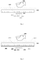
Fig. 1 , in basic architecture of a conventional under-display fingerprint identification module, an Organic Light-Emitting Diode (OLED) is used as the transmitting unit, i.e., a light source. When the screen is touched by afinger 100, a light beam transmitted by the OLED is reflected or refracted, and the reflected light beam is received by an optical fingerprint identification module arranged under the screen so as to achieve the under-display fingerprint identification. Thefingerprint identification module 101 is attached onto ascreen assembly 102 through an adhesive 103, and it includes abracket 1011, an infrared (IR)color filter 1012, anoptical collimator 1013, asealant 1014 andimage sensor 1015. Theoptical collimator 1013 is mainly used for collimate the reflected light through a collimating aperture toward theimage sensor 1015, so as to achieve optical energy isolation with respect to light beams for pixels of theimage sensor 1015, thereby to prevent the occurrence of light crosstalk among the sensing pixels. TheIR color filter 1012 includes a glass base substrate and an IR material coating, so as to prevent the IR interference caused by external sunlight, thereby to prevent the failure of the fingerprint identification due to the intensive light when a user is outdoors. - As a main drawback, the optical fingerprint identification module is susceptible to the intensive light. Hence, the
fingerprint identification module 101 needs to perform infrared filtration through theIR color filter 1012, so as to prevent the infrared light from interfering with theimage sensor 1015. Generally, thefingerprint identification module 101 has a separate structure of glass color filter, and the color filter is arranged above thefingerprint identification module 101 for the infrared filtration. However, the color filter has a thickness of about 0.11mm, resulting in a constraint to a space design of the electronic device to some extent. - In one aspect, the present disclosure provides a fingerprint identification module for an electronic device, the electronic device including a screen assembly provided with a glass substrate, the fingerprint identification module including: a color filter coating applied onto the glass substrate; an optical collimator arranged at a side of the color filter coating away from the glass substrate; and an image sensor arranged at a side of the optical collimator away from the color filter coating.
- In another aspect, the present disclosure provides in some embodiments an electronic device including the above-mentioned fingerprint identification module.
- In order to illustrate the technical solutions of the present disclosure or the related art in a clearer manner, the drawings desired for the present disclosure or the related art will be described hereinafter briefly. Obviously, the following drawings merely relate to some embodiments of the present disclosure, and based on these drawings, a person skilled in the art may obtain the other drawings without any creative effort.
-
Fig.1 is a schematic view showing a fingerprint identification module in the related art; -
Fig.2 is a schematic view showing a fingerprint identification module according to one embodiment of the present disclosure; and -
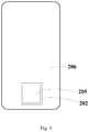
Fig.3 is a schematic view showing a position relationship between a color filter coating and a module bracket inFig.2 . -
- 100
- finger
- 101
- fingerprint identification module
- 102
- screen assembly
- 103
- adhesive
- 1011
- bracket
- 1012
- IR color filter
- 1013
- optical collimator
- 1014
- sealant
- 1015
- image sensor
- 201
- screen assembly
- 202
- color filter coating
- 203
- optical collimator
- 204
- image sensor
- 205
- module bracket
- 206
- protection coating
- 2011
- glass substrate
- 2012
- OLED panel unit
- 2013
- glass cover plate
- The present disclosure will be described hereinafter in conjunction with the drawings and embodiments. The following embodiments are for illustrative purposes only, but shall not be used to limit the scope of the present disclosure. Actually, the embodiments are provided so as to facilitate the understanding of the scope of the present disclosure.
- In the embodiments of the present disclosure, such words as "in the middle of', "longitudinal", "lateral", "length", "width", "thickness", "on/above", "under/below", "front", "back", "left", "right", "vertical", "horizontal", "top", "bottom", "inside", "outside", "clockwise", "counter-clockwise", "axial", "radial" and "circumferential" may be used to indicate directions or positions as viewed in the drawings, and they are merely used to facilitate the description in the present disclosure, rather than to indicate or imply that a device or member must be arranged or operated at a specific position.
- In addition, such words as "first" and "second" are merely used to differentiate different components rather than to represent any order, number or importance, i.e., they are used to implicitly or explicitly indicate that there is at least one component. Further, such a phrase as "a plurality of' is used to indicate that there are at least two, e.g., two or three, components, unless otherwise specified.
- Unless otherwise specified, such words as "arrange", "connect" and "fix" may have a general meaning, e.g., the word "connect" may refer to fixed connection, removable connection or integral connection, or mechanical or electrical connection, or direct connection or indirect connection via an intermediate component, or communication between two components, or wired or wireless communication connection. The meanings of these words may be understood by a person skilled in the art in accordance with the practical need.
- Unless otherwise defined, when one member is arranged on or under another member, the member may be in contact with the other member directly or via an intermediate member. In addition, when one member is arranged on/above another member, the member may be arranged right on/above the other member or not, or it merely means that the member is located at a level higher than the other member. When one member is arranged under/below another member, the member may be arranged right under/below the other member or not, or it merely means that the member is located at a level lower than the other member.
- An object of the present disclosure is to provide a fingerprint identification module and an electronic device, so as to solve the problem in the related art where a thickness of the entire fingerprint identification module increases and a space design of the electronic device is limited due to a structural thickness of a color filter in the fingerprint identification module.
- As shown in
Fig.2 , the present disclosure provides in some embodiments a fingerprint identification module for an electronic device. The electronic device includes ascreen assembly 201 provided with aglass substrate 2011. The fingerprint identification module includes acolor filter coating 202, anoptical collimator 203 and animage sensor 204. Thecolor filter coating 202 is applied onto theglass substrate 2011, theoptical collimator 203 is arranged at a side of thecolor filter coating 202 away from theglass substrate 2011, and theimage sensor 204 is arranged at a side of theoptical collimator 203 away from thecolor filter coating 202. In the fingerprint identification module, theoptical collimator 203 and theimage sensor 204 may be encapsulated to form an encapsulation structure, and thecolor filter coating 202 may be applied onto theglass substrate 2011 to form a color filter structure capable of preventing the interference caused by external intensive light. In this way, the color filter structure may be separated from the encapsulation structure of the fingerprint identification module, and thecolor filter coating 202 may be directly attached onto theglass substrate 2011 at an inner side of the screen assembly 201 (a side of thescreen assembly 201 facing a user is an outer side, and a side of thescreen assembly 201 mounted on a middle frame structure is the inner side). As a result, it is unnecessary to provide a color filter structure in the encapsulation structure of the fingerprint identification module in a conventional scheme, so it is able to reduce a thickness of the entire fingerprint identification module. - In the embodiments of the present disclosure, the fingerprint identification module may further include a
module bracket 205 onto which theoptical collimator 203 and theimage sensor 204 are installed. Themodule bracket 205 may be fixed onto theglass substrate 2011 at a position where thecolor filter coating 202 is applied. In other words, theoptical collimator 203 and theimage sensor 204 may be encapsulated through themodule bracket 205 to form the encapsulation structure, and then fixed onto theglass substrate 2011 through themodule bracket 205. Further, an edge of each of theoptical collimator 203 and theimage sensor 204 may be fixed onto themodule bracket 205. To be specific, the edge of each of theoptical collimator 203 and theimage sensor 204 may be adhered to themodule bracket 205 through an adhesive, and themodule bracket 205 may be adhered onto theglass substrate 2011 through an adhesive too. - Further, as shown in
Fig.3 , an area of thecolor filter coating 202 may be greater than or equal to an installation coverage area of themodule bracket 205 and theglass substrate 2011, i.e., greater than or equal to an area of an upper surface of the encapsulation structure of the fingerprint identification module. In this way, after the fingerprint identification module has been adhered onto the glass substrate, it is able for thecolor filter coating 202 to prevent the intensive light from interfering with the fingerprint identification module in a more efficient manner. - As shown in
Fig.2 , thescreen assembly 201 may further include anOLED panel unit 2012 arranged at a side of theglass substrate 2011 away from thecolor filter coating 202, and aglass cover plate 2013 arranged at a side of theOLED panel unit 2012 away from theglass substrate 2011. TheOLED panel unit 2012 may serve as a light source. When a panel is touched by thefinger 100, a light beam emitted by theOLED panel unit 201 may be reflected or refracted, and the reflected light beam may be received by the fingerprint identification module under the screen assembly, so as to achieve the under-display fingerprint identification. To be specific, theOLED panel unit 2012 may be provided with at least one OLED, and the quantity and an arrangement mode of the OLEDs will not be particularly defined herein. - As shown in
Fig.2 , aprotection coating 206 may be applied to a side of theglass substrate 2011 away from theOLED panel unit 2012 at a region other than the region where thecolor filter coating 202 is located. In other words, a protection film may be applied onto theglass substrate 2011 other than the region where thecolor filter layer 202 is located. During the manufacture, before the application of thecolor filter coating 202, a certain region of the glass substrate may be exposed, and thecolor filter coating 202 may be applied to the certain region. - According to the fingerprint identification module in the embodiments of the present disclosure, the color filter coating may be applied onto the glass substrate of the screen assembly, i.e., it is unnecessary to provide a separate color filter as compared with a conventional fingerprint identification module, so it is able to reduce a structural thickness of the fingerprint identification module, thereby to release a design space of the electronic device. Further, the area of the color filter coating may be greater than the area of installation surface of the encapsulation structure in the fingerprint identification module, so it is able to prevent the leakage of infrared light due to the encapsulation of the color filter in the fingerprint identification module, thereby to improve the resistance to intensive light.
- The present disclosure further provides in some embodiments an electronic device which includes the above-mentioned fingerprint identification module. The implementation of the electronic device may refer to that of the fingerprint identification module with a same technical effect. The electronic device may be a mobile phone, a laptop computer, a Personal Digital Assistant (PDA), a vehicle-mounted computer, a music player, an e-book or a navigator. According to the electronic device in the embodiments of the present disclosure, the color filter coating may be applied onto the glass substrate of the screen assembly, i.e., it is unnecessary to provide a separate color filter as compared with the conventional fingerprint identification module, so it is able to reduce the structural thickness of the fingerprint identification module, thereby to release the design space of the electronic device.
- The above embodiments have been described in a progressive manner, and the same or similar contents in the embodiments will not be repeated, i.e., each embodiment merely focuses on the difference from the others.
- Although the preferred embodiments are described above, a person skilled in the art may make modifications and alterations to these embodiments in accordance with the basic concept of the present disclosure. So, the appended claims are intended to include the preferred embodiments and all of the modifications and alterations that fall within the scope of the present disclosure.
- It should be further appreciated that, such words as "first" and "second" are merely used to separate one entity or operation from another entity or operation, but are not necessarily used to represent or imply any relation or order between the entities or operations. In addition, such terms as "include" or "including" or any other variations involved in the present disclosure intend to provide non-exclusive coverage, so that a procedure, method, article or device including a series of elements may also include any other elements not listed herein, or may include any inherent elements of the procedure, method, article or device. If without any further limitations, for the elements defined by such sentence as "including one ...", it is not excluded that the procedure, method, article or device including the elements may also include any other identical elements.
- The above embodiments are for illustrative purposes only, but the present disclosure is not limited thereto. Obviously, a person skilled in the art may make further modifications and improvements without departing from the spirit of the present disclosure, and these modifications and improvements shall also fall within the scope of the present disclosure.
Claims (10)
- A fingerprint identification module applied for an electronic device, wherein the electronic device comprises a screen assembly (201) provided with a glass substrate (2011), the fingerprint identification module comprises:a color filter coating (202) applied onto the glass substrate (2011);an optical collimator (203) arranged at a side of the color filter coating (202) away from the glass substrate (2011); andan image sensor (204) arranged at a side of the optical collimator (203) away from the color filter coating (202).
- The fingerprint identification module according to claim 1, further comprising a module bracket (205) onto which the optical collimator (203) and the image sensor (204) are installed, wherein the module bracket (205) is fixed onto the glass substrate (2011) at a position where the color filter coating (202) is applied.
- The fingerprint identification module according to claim 2, wherein an area of the color filter coating (202) is greater than or equal to an installation coverage area of the module bracket (205) and the glass substrate (2011).
- The fingerprint identification module according to claim 2, wherein an edge of each of the optical collimator (203) and the image sensor (204) is fixed onto the module bracket (205).
- The fingerprint identification module according to claim 4, wherein the edge of each of the optical collimator (203) and the image sensor (204) is adhered onto the module bracket (205), and the module bracket (205) is adhered onto the glass substrate (2011).
- The fingerprint identification module according to claim 1, wherein the screen assembly (201) further comprises an Organic Light-Emitting Diode (OLED) panel unit 2012 arranged at a side of the glass substrate (2011) away from the color filter coating (202) and a glass cover plate (2013) arranged at a side of the OLED panel unit (2012) away from the glass substrate (2011).
- The fingerprint identification module according to claim 6, wherein the OLED panel unit (2012) is provided with at least one OLED.
- The fingerprint identification module according to claim 6, wherein a protection coating (206) is applied to a side of the glass substrate (2011) away from the OLED panel unit (2012) at a region other than a region where the color filter coating (202) is located.
- An electronic device, comprising the fingerprint identification module according to any one of claims 1 to 8.
- The electronic device according to claim 9, wherein the electronic device is a mobile phone, a laptop computer, a personal digital assistant, a vehicle-mounted computer, a music player, an e-book or a navigator.
Applications Claiming Priority (2)
| Application Number | Priority Date | Filing Date | Title |
|---|---|---|---|
| CN201711475779.2A CN107958237A (en) | 2017-12-29 | 2017-12-29 | A kind of fingerprint recognition module and electronic equipment |
| PCT/CN2018/125407 WO2019129265A1 (en) | 2017-12-29 | 2018-12-29 | Fingerprint identification module and electronic device |
Publications (3)
| Publication Number | Publication Date |
|---|---|
| EP3734497A1 true EP3734497A1 (en) | 2020-11-04 |
| EP3734497A4 EP3734497A4 (en) | 2021-02-24 |
| EP3734497B1 EP3734497B1 (en) | 2024-07-10 |
Family
ID=61956169
Family Applications (1)
| Application Number | Title | Priority Date | Filing Date |
|---|---|---|---|
| EP18894137.1A Active EP3734497B1 (en) | 2017-12-29 | 2018-12-29 | Fingerprint identification module and electronic device |
Country Status (5)
| Country | Link |
|---|---|
| US (1) | US11151354B2 (en) |
| EP (1) | EP3734497B1 (en) |
| CN (1) | CN107958237A (en) |
| ES (1) | ES2986510T3 (en) |
| WO (1) | WO2019129265A1 (en) |
Families Citing this family (16)
| Publication number | Priority date | Publication date | Assignee | Title |
|---|---|---|---|---|
| CN107958237A (en) * | 2017-12-29 | 2018-04-24 | 维沃移动通信有限公司 | A kind of fingerprint recognition module and electronic equipment |
| CN108598117B (en) * | 2018-04-25 | 2021-03-12 | 京东方科技集团股份有限公司 | Display device and fingerprint identification method of display device |
| KR102623375B1 (en) * | 2018-06-08 | 2024-01-11 | 삼성디스플레이 주식회사 | Display device and method for manufacturing the display device |
| EP3798896B1 (en) | 2018-08-21 | 2022-11-23 | Shenzhen Goodix Technology Co., Ltd. | Lens system, fingerprint recognition apparatus, and terminal device |
| CN109284734A (en) * | 2018-10-15 | 2019-01-29 | Oppo广东移动通信有限公司 | Fingerprint identification module, display device and electronic equipment |
| WO2020087242A1 (en) * | 2018-10-30 | 2020-05-07 | 深圳市汇顶科技股份有限公司 | In-display optical fingerprint device and handheld device having optical fingerprint anti-counterfeiting sensing function |
| CN111245981B (en) * | 2018-11-29 | 2021-06-22 | 北京小米移动软件有限公司 | Mobile terminal and LCD module |
| CN111259693B (en) * | 2018-11-30 | 2024-02-09 | 北京小米移动软件有限公司 | Sensor modules and mobile terminals |
| CN109753919B (en) * | 2018-12-29 | 2021-04-02 | 武汉华星光电技术有限公司 | Optical fingerprint identification device |
| CN111832359B (en) * | 2019-04-19 | 2025-04-15 | 格科微电子(上海)有限公司 | Method for reducing the height of optical fingerprint recognition module |
| WO2021012117A1 (en) * | 2019-07-19 | 2021-01-28 | 深圳市汇顶科技股份有限公司 | Under-screen optical fingerprint recognition apparatus and system, diffusion film, and liquid crystal display |
| CN112434272B (en) * | 2019-08-26 | 2022-12-20 | 英业达科技有限公司 | electronic device |
| CN110543847B (en) | 2019-08-29 | 2021-04-02 | 维沃移动通信有限公司 | Display module and electronic equipment |
| CN110738939B (en) * | 2019-10-31 | 2021-10-15 | 维沃移动通信有限公司 | Electronic equipment |
| CN112906443A (en) * | 2019-12-04 | 2021-06-04 | 北京小米移动软件有限公司 | Fingerprint identification module and mobile terminal |
| CN113536872B (en) | 2020-04-22 | 2023-10-13 | 群创光电股份有限公司 | Fingerprint recognition module and fingerprint recognition device |
Family Cites Families (13)
| Publication number | Priority date | Publication date | Assignee | Title |
|---|---|---|---|---|
| KR100724135B1 (en) * | 2001-10-05 | 2007-06-04 | 신에쓰 가가꾸 고교 가부시끼가이샤 | Perfluoropolyether-modified silanes, surface treatment agents, and antireflective filters |
| US7924272B2 (en) | 2006-11-27 | 2011-04-12 | Microsoft Corporation | Infrared sensor integrated in a touch panel |
| CN202647304U (en) | 2012-06-01 | 2013-01-02 | 东华大学 | Myopia-preventing LED lamp |
| CN103943645B (en) | 2014-05-20 | 2019-04-23 | 苏州晶方半导体科技股份有限公司 | Image sensor module and method of forming the same |
| US10049256B2 (en) * | 2015-12-11 | 2018-08-14 | Gingy Technology Inc. | Fingerprint sensing module |
| CN204258907U (en) | 2014-09-22 | 2015-04-08 | 郭进锋 | A kind of CIS scanner gathering palm vein image |
| CN104615979A (en) * | 2015-01-27 | 2015-05-13 | 华进半导体封装先导技术研发中心有限公司 | Fingerprint identification module and encapsulation method thereof, and fingerprint identification module group and encapsulation method thereof |
| US10229316B2 (en) * | 2016-01-29 | 2019-03-12 | Synaptics Incorporated | Compound collimating system using apertures and collimators |
| KR102493607B1 (en) * | 2016-06-15 | 2023-02-01 | 삼성전자주식회사 | Electronic device for supporting the fingerprint verification and operating method thereof |
| CN106960201A (en) * | 2017-04-07 | 2017-07-18 | 惠州凯珑光电有限公司 | A kind of optical finger print module |
| CN107092402A (en) * | 2017-04-19 | 2017-08-25 | 维沃移动通信有限公司 | A kind of display screen and electronic equipment |
| CN107092492B (en) | 2017-04-27 | 2019-02-12 | 广州四三九九信息科技有限公司 | The control method and device of virtual objects |
| CN107958237A (en) | 2017-12-29 | 2018-04-24 | 维沃移动通信有限公司 | A kind of fingerprint recognition module and electronic equipment |
-
2017
- 2017-12-29 CN CN201711475779.2A patent/CN107958237A/en active Pending
-
2018
- 2018-12-29 WO PCT/CN2018/125407 patent/WO2019129265A1/en not_active Ceased
- 2018-12-29 US US16/958,581 patent/US11151354B2/en active Active
- 2018-12-29 ES ES18894137T patent/ES2986510T3/en active Active
- 2018-12-29 EP EP18894137.1A patent/EP3734497B1/en active Active
Also Published As
| Publication number | Publication date |
|---|---|
| US20200356749A1 (en) | 2020-11-12 |
| US11151354B2 (en) | 2021-10-19 |
| WO2019129265A1 (en) | 2019-07-04 |
| CN107958237A (en) | 2018-04-24 |
| ES2986510T3 (en) | 2024-11-11 |
| EP3734497A4 (en) | 2021-02-24 |
| EP3734497B1 (en) | 2024-07-10 |
Similar Documents
| Publication | Publication Date | Title |
|---|---|---|
| EP3734497B1 (en) | Fingerprint identification module and electronic device | |
| US10599907B2 (en) | Display panel for fingerprint recognition and display device | |
| EP3428967B1 (en) | Electronic device having display | |
| US20220020321A1 (en) | Electronic device having display | |
| TWI722070B (en) | Display device | |
| US20190102593A1 (en) | Fingerprint identification display device | |
| CN107393907B (en) | Display panels and display devices | |
| US11309521B2 (en) | Flexible display module having a hollow defined middle | |
| US20180211088A1 (en) | Electronic device having a biometric sensor | |
| CN110045863B (en) | Touch panel and display device | |
| JP2016538586A (en) | Display module and system application | |
| CN210955904U (en) | Display substrate, display panel and display device | |
| US10884528B2 (en) | Touch display substrate and touch detection method thereof | |
| US20140140092A1 (en) | Back light module and display device using the same | |
| CN207924309U (en) | Display device | |
| CN108470758A (en) | Organic light emitting display panel and display device | |
| US20200006456A1 (en) | Display panel, display device, and manufacturing method of display panel | |
| US10777624B2 (en) | Display assembly and manufacturing method thereof and display apparatus | |
| US11726359B2 (en) | Display module and electronic device | |
| CN115172626B (en) | Display panel and display device | |
| WO2021115308A1 (en) | Display screen module and electronic device | |
| CN108090480A (en) | The production method of display panel, display device and display panel | |
| US20220115443A1 (en) | Display device and image sensing method thereof | |
| KR102501537B1 (en) | Cover window for electronic device and electronic device comprising the same | |
| CN210721495U (en) | Flexible electronic equipment with fingerprint identification function |
Legal Events
| Date | Code | Title | Description |
|---|---|---|---|
| STAA | Information on the status of an ep patent application or granted ep patent |
Free format text: STATUS: THE INTERNATIONAL PUBLICATION HAS BEEN MADE |
|
| PUAI | Public reference made under article 153(3) epc to a published international application that has entered the european phase |
Free format text: ORIGINAL CODE: 0009012 |
|
| STAA | Information on the status of an ep patent application or granted ep patent |
Free format text: STATUS: REQUEST FOR EXAMINATION WAS MADE |
|
| 17P | Request for examination filed |
Effective date: 20200630 |
|
| AK | Designated contracting states |
Kind code of ref document: A1 Designated state(s): AL AT BE BG CH CY CZ DE DK EE ES FI FR GB GR HR HU IE IS IT LI LT LU LV MC MK MT NL NO PL PT RO RS SE SI SK SM TR |
|
| AX | Request for extension of the european patent |
Extension state: BA ME |
|
| A4 | Supplementary search report drawn up and despatched |
Effective date: 20210125 |
|
| RIC1 | Information provided on ipc code assigned before grant |
Ipc: G06F 3/042 20060101ALI20210119BHEP Ipc: G06K 9/00 20060101AFI20210119BHEP |
|
| DAV | Request for validation of the european patent (deleted) | ||
| DAX | Request for extension of the european patent (deleted) | ||
| STAA | Information on the status of an ep patent application or granted ep patent |
Free format text: STATUS: EXAMINATION IS IN PROGRESS |
|
| 17Q | First examination report despatched |
Effective date: 20221207 |
|
| REG | Reference to a national code |
Ref country code: DE Ref legal event code: R079 Free format text: PREVIOUS MAIN CLASS: G06K0009000000 Ipc: G06V0010143000 Ref country code: DE Ref legal event code: R079 Ref document number: 602018071716 Country of ref document: DE Free format text: PREVIOUS MAIN CLASS: G06K0009000000 Ipc: G06V0010143000 |
|
| GRAP | Despatch of communication of intention to grant a patent |
Free format text: ORIGINAL CODE: EPIDOSNIGR1 |
|
| STAA | Information on the status of an ep patent application or granted ep patent |
Free format text: STATUS: GRANT OF PATENT IS INTENDED |
|
| RIC1 | Information provided on ipc code assigned before grant |
Ipc: G06V 40/13 20220101ALI20240214BHEP Ipc: G06V 10/143 20220101AFI20240214BHEP |
|
| INTG | Intention to grant announced |
Effective date: 20240311 |
|
| GRAS | Grant fee paid |
Free format text: ORIGINAL CODE: EPIDOSNIGR3 |
|
| GRAA | (expected) grant |
Free format text: ORIGINAL CODE: 0009210 |
|
| STAA | Information on the status of an ep patent application or granted ep patent |
Free format text: STATUS: THE PATENT HAS BEEN GRANTED |
|
| AK | Designated contracting states |
Kind code of ref document: B1 Designated state(s): AL AT BE BG CH CY CZ DE DK EE ES FI FR GB GR HR HU IE IS IT LI LT LU LV MC MK MT NL NO PL PT RO RS SE SI SK SM TR |
|
| REG | Reference to a national code |
Ref country code: CH Ref legal event code: EP |
|
| REG | Reference to a national code |
Ref country code: DE Ref legal event code: R096 Ref document number: 602018071716 Country of ref document: DE |
|
| REG | Reference to a national code |
Ref country code: NL Ref legal event code: FP |
|
| REG | Reference to a national code |
Ref country code: LT Ref legal event code: MG9D Ref country code: ES Ref legal event code: FG2A Ref document number: 2986510 Country of ref document: ES Kind code of ref document: T3 Effective date: 20241111 |
|
| PG25 | Lapsed in a contracting state [announced via postgrant information from national office to epo] |
Ref country code: PT Free format text: LAPSE BECAUSE OF FAILURE TO SUBMIT A TRANSLATION OF THE DESCRIPTION OR TO PAY THE FEE WITHIN THE PRESCRIBED TIME-LIMIT Effective date: 20241111 |
|
| REG | Reference to a national code |
Ref country code: AT Ref legal event code: MK05 Ref document number: 1702723 Country of ref document: AT Kind code of ref document: T Effective date: 20240710 |
|
| PG25 | Lapsed in a contracting state [announced via postgrant information from national office to epo] |
Ref country code: PT Free format text: LAPSE BECAUSE OF FAILURE TO SUBMIT A TRANSLATION OF THE DESCRIPTION OR TO PAY THE FEE WITHIN THE PRESCRIBED TIME-LIMIT Effective date: 20241111 |
|
| PG25 | Lapsed in a contracting state [announced via postgrant information from national office to epo] |
Ref country code: NO Free format text: LAPSE BECAUSE OF FAILURE TO SUBMIT A TRANSLATION OF THE DESCRIPTION OR TO PAY THE FEE WITHIN THE PRESCRIBED TIME-LIMIT Effective date: 20241010 |
|
| PG25 | Lapsed in a contracting state [announced via postgrant information from national office to epo] |
Ref country code: PL Free format text: LAPSE BECAUSE OF FAILURE TO SUBMIT A TRANSLATION OF THE DESCRIPTION OR TO PAY THE FEE WITHIN THE PRESCRIBED TIME-LIMIT Effective date: 20240710 Ref country code: GR Free format text: LAPSE BECAUSE OF FAILURE TO SUBMIT A TRANSLATION OF THE DESCRIPTION OR TO PAY THE FEE WITHIN THE PRESCRIBED TIME-LIMIT Effective date: 20241011 Ref country code: FI Free format text: LAPSE BECAUSE OF FAILURE TO SUBMIT A TRANSLATION OF THE DESCRIPTION OR TO PAY THE FEE WITHIN THE PRESCRIBED TIME-LIMIT Effective date: 20240710 |
|
| PG25 | Lapsed in a contracting state [announced via postgrant information from national office to epo] |
Ref country code: BG Free format text: LAPSE BECAUSE OF FAILURE TO SUBMIT A TRANSLATION OF THE DESCRIPTION OR TO PAY THE FEE WITHIN THE PRESCRIBED TIME-LIMIT Effective date: 20240710 |
|
| PG25 | Lapsed in a contracting state [announced via postgrant information from national office to epo] |
Ref country code: LV Free format text: LAPSE BECAUSE OF FAILURE TO SUBMIT A TRANSLATION OF THE DESCRIPTION OR TO PAY THE FEE WITHIN THE PRESCRIBED TIME-LIMIT Effective date: 20240710 |
|
| PG25 | Lapsed in a contracting state [announced via postgrant information from national office to epo] |
Ref country code: IS Free format text: LAPSE BECAUSE OF FAILURE TO SUBMIT A TRANSLATION OF THE DESCRIPTION OR TO PAY THE FEE WITHIN THE PRESCRIBED TIME-LIMIT Effective date: 20241110 Ref country code: AT Free format text: LAPSE BECAUSE OF FAILURE TO SUBMIT A TRANSLATION OF THE DESCRIPTION OR TO PAY THE FEE WITHIN THE PRESCRIBED TIME-LIMIT Effective date: 20240710 |
|
| PG25 | Lapsed in a contracting state [announced via postgrant information from national office to epo] |
Ref country code: HR Free format text: LAPSE BECAUSE OF FAILURE TO SUBMIT A TRANSLATION OF THE DESCRIPTION OR TO PAY THE FEE WITHIN THE PRESCRIBED TIME-LIMIT Effective date: 20240710 |
|
| PG25 | Lapsed in a contracting state [announced via postgrant information from national office to epo] |
Ref country code: RS Free format text: LAPSE BECAUSE OF FAILURE TO SUBMIT A TRANSLATION OF THE DESCRIPTION OR TO PAY THE FEE WITHIN THE PRESCRIBED TIME-LIMIT Effective date: 20241010 |
|
| PG25 | Lapsed in a contracting state [announced via postgrant information from national office to epo] |
Ref country code: RS Free format text: LAPSE BECAUSE OF FAILURE TO SUBMIT A TRANSLATION OF THE DESCRIPTION OR TO PAY THE FEE WITHIN THE PRESCRIBED TIME-LIMIT Effective date: 20241010 Ref country code: PL Free format text: LAPSE BECAUSE OF FAILURE TO SUBMIT A TRANSLATION OF THE DESCRIPTION OR TO PAY THE FEE WITHIN THE PRESCRIBED TIME-LIMIT Effective date: 20240710 Ref country code: NO Free format text: LAPSE BECAUSE OF FAILURE TO SUBMIT A TRANSLATION OF THE DESCRIPTION OR TO PAY THE FEE WITHIN THE PRESCRIBED TIME-LIMIT Effective date: 20241010 Ref country code: LV Free format text: LAPSE BECAUSE OF FAILURE TO SUBMIT A TRANSLATION OF THE DESCRIPTION OR TO PAY THE FEE WITHIN THE PRESCRIBED TIME-LIMIT Effective date: 20240710 Ref country code: IS Free format text: LAPSE BECAUSE OF FAILURE TO SUBMIT A TRANSLATION OF THE DESCRIPTION OR TO PAY THE FEE WITHIN THE PRESCRIBED TIME-LIMIT Effective date: 20241110 Ref country code: HR Free format text: LAPSE BECAUSE OF FAILURE TO SUBMIT A TRANSLATION OF THE DESCRIPTION OR TO PAY THE FEE WITHIN THE PRESCRIBED TIME-LIMIT Effective date: 20240710 Ref country code: GR Free format text: LAPSE BECAUSE OF FAILURE TO SUBMIT A TRANSLATION OF THE DESCRIPTION OR TO PAY THE FEE WITHIN THE PRESCRIBED TIME-LIMIT Effective date: 20241011 Ref country code: FI Free format text: LAPSE BECAUSE OF FAILURE TO SUBMIT A TRANSLATION OF THE DESCRIPTION OR TO PAY THE FEE WITHIN THE PRESCRIBED TIME-LIMIT Effective date: 20240710 Ref country code: BG Free format text: LAPSE BECAUSE OF FAILURE TO SUBMIT A TRANSLATION OF THE DESCRIPTION OR TO PAY THE FEE WITHIN THE PRESCRIBED TIME-LIMIT Effective date: 20240710 Ref country code: AT Free format text: LAPSE BECAUSE OF FAILURE TO SUBMIT A TRANSLATION OF THE DESCRIPTION OR TO PAY THE FEE WITHIN THE PRESCRIBED TIME-LIMIT Effective date: 20240710 |
|
| REG | Reference to a national code |
Ref country code: DE Ref legal event code: R097 Ref document number: 602018071716 Country of ref document: DE |
|
| PG25 | Lapsed in a contracting state [announced via postgrant information from national office to epo] |
Ref country code: DK Free format text: LAPSE BECAUSE OF FAILURE TO SUBMIT A TRANSLATION OF THE DESCRIPTION OR TO PAY THE FEE WITHIN THE PRESCRIBED TIME-LIMIT Effective date: 20240710 Ref country code: RO Free format text: LAPSE BECAUSE OF FAILURE TO SUBMIT A TRANSLATION OF THE DESCRIPTION OR TO PAY THE FEE WITHIN THE PRESCRIBED TIME-LIMIT Effective date: 20240710 Ref country code: SM Free format text: LAPSE BECAUSE OF FAILURE TO SUBMIT A TRANSLATION OF THE DESCRIPTION OR TO PAY THE FEE WITHIN THE PRESCRIBED TIME-LIMIT Effective date: 20240710 |
|
| PG25 | Lapsed in a contracting state [announced via postgrant information from national office to epo] |
Ref country code: EE Free format text: LAPSE BECAUSE OF FAILURE TO SUBMIT A TRANSLATION OF THE DESCRIPTION OR TO PAY THE FEE WITHIN THE PRESCRIBED TIME-LIMIT Effective date: 20240710 |
|
| PG25 | Lapsed in a contracting state [announced via postgrant information from national office to epo] |
Ref country code: CZ Free format text: LAPSE BECAUSE OF FAILURE TO SUBMIT A TRANSLATION OF THE DESCRIPTION OR TO PAY THE FEE WITHIN THE PRESCRIBED TIME-LIMIT Effective date: 20240710 |
|
| PG25 | Lapsed in a contracting state [announced via postgrant information from national office to epo] |
Ref country code: SK Free format text: LAPSE BECAUSE OF FAILURE TO SUBMIT A TRANSLATION OF THE DESCRIPTION OR TO PAY THE FEE WITHIN THE PRESCRIBED TIME-LIMIT Effective date: 20240710 |
|
| PLBE | No opposition filed within time limit |
Free format text: ORIGINAL CODE: 0009261 |
|
| STAA | Information on the status of an ep patent application or granted ep patent |
Free format text: STATUS: NO OPPOSITION FILED WITHIN TIME LIMIT |
|
| 26N | No opposition filed |
Effective date: 20250411 |
|
| PG25 | Lapsed in a contracting state [announced via postgrant information from national office to epo] |
Ref country code: MC Free format text: LAPSE BECAUSE OF FAILURE TO SUBMIT A TRANSLATION OF THE DESCRIPTION OR TO PAY THE FEE WITHIN THE PRESCRIBED TIME-LIMIT Effective date: 20240710 |
|
| REG | Reference to a national code |
Ref country code: CH Ref legal event code: PL |
|
| PG25 | Lapsed in a contracting state [announced via postgrant information from national office to epo] |
Ref country code: LU Free format text: LAPSE BECAUSE OF NON-PAYMENT OF DUE FEES Effective date: 20241229 |
|
| PG25 | Lapsed in a contracting state [announced via postgrant information from national office to epo] |
Ref country code: SE Free format text: LAPSE BECAUSE OF FAILURE TO SUBMIT A TRANSLATION OF THE DESCRIPTION OR TO PAY THE FEE WITHIN THE PRESCRIBED TIME-LIMIT Effective date: 20240710 |
|
| REG | Reference to a national code |
Ref country code: BE Ref legal event code: MM Effective date: 20241231 |
|
| PG25 | Lapsed in a contracting state [announced via postgrant information from national office to epo] |
Ref country code: BE Free format text: LAPSE BECAUSE OF NON-PAYMENT OF DUE FEES Effective date: 20241231 |
|
| PG25 | Lapsed in a contracting state [announced via postgrant information from national office to epo] |
Ref country code: CH Free format text: LAPSE BECAUSE OF NON-PAYMENT OF DUE FEES Effective date: 20241231 |
|
| PG25 | Lapsed in a contracting state [announced via postgrant information from national office to epo] |
Ref country code: IE Free format text: LAPSE BECAUSE OF NON-PAYMENT OF DUE FEES Effective date: 20241229 |
|
| PGFP | Annual fee paid to national office [announced via postgrant information from national office to epo] |
Ref country code: NL Payment date: 20251112 Year of fee payment: 8 |
|
| PGFP | Annual fee paid to national office [announced via postgrant information from national office to epo] |
Ref country code: DE Payment date: 20251104 Year of fee payment: 8 |
|
| PGFP | Annual fee paid to national office [announced via postgrant information from national office to epo] |
Ref country code: GB Payment date: 20251114 Year of fee payment: 8 |
|
| PGFP | Annual fee paid to national office [announced via postgrant information from national office to epo] |
Ref country code: IT Payment date: 20251121 Year of fee payment: 8 |
|
| PGFP | Annual fee paid to national office [announced via postgrant information from national office to epo] |
Ref country code: FR Payment date: 20251110 Year of fee payment: 8 |
|
| PGFP | Annual fee paid to national office [announced via postgrant information from national office to epo] |
Ref country code: ES Payment date: 20260113 Year of fee payment: 8 |
|
| PG25 | Lapsed in a contracting state [announced via postgrant information from national office to epo] |
Ref country code: CY Free format text: LAPSE BECAUSE OF FAILURE TO SUBMIT A TRANSLATION OF THE DESCRIPTION OR TO PAY THE FEE WITHIN THE PRESCRIBED TIME-LIMIT Effective date: 20240710 |
|
| REG | Reference to a national code |
Ref country code: GB Ref legal event code: 732E Free format text: REGISTERED BETWEEN 20260409 AND 20260415 |