EP3734464A1 - Integrated filter for de-sense reduction - Google Patents
Integrated filter for de-sense reduction Download PDFInfo
- Publication number
- EP3734464A1 EP3734464A1 EP20170341.0A EP20170341A EP3734464A1 EP 3734464 A1 EP3734464 A1 EP 3734464A1 EP 20170341 A EP20170341 A EP 20170341A EP 3734464 A1 EP3734464 A1 EP 3734464A1
- Authority
- EP
- European Patent Office
- Prior art keywords
- signal
- chip
- interface
- ground
- chip package
- Prior art date
- Legal status (The legal status is an assumption and is not a legal conclusion. Google has not performed a legal analysis and makes no representation as to the accuracy of the status listed.)
- Granted
Links
Images






Classifications
-
- G—PHYSICS
- G06—COMPUTING OR CALCULATING; COUNTING
- G06F—ELECTRIC DIGITAL DATA PROCESSING
- G06F13/00—Interconnection of, or transfer of information or other signals between, memories, input/output devices or central processing units
- G06F13/38—Information transfer, e.g. on bus
- G06F13/40—Bus structure
- G06F13/4063—Device-to-bus coupling
- G06F13/4068—Electrical coupling
-
- H—ELECTRICITY
- H01—ELECTRIC ELEMENTS
- H01P—WAVEGUIDES; RESONATORS, LINES, OR OTHER DEVICES OF THE WAVEGUIDE TYPE
- H01P1/00—Auxiliary devices
- H01P1/20—Frequency-selective devices, e.g. filters
-
- H—ELECTRICITY
- H05—ELECTRIC TECHNIQUES NOT OTHERWISE PROVIDED FOR
- H05K—PRINTED CIRCUITS; CASINGS OR CONSTRUCTIONAL DETAILS OF ELECTRIC APPARATUS; MANUFACTURE OF ASSEMBLAGES OF ELECTRICAL COMPONENTS
- H05K1/00—Printed circuits
- H05K1/02—Details
- H05K1/0213—Electrical arrangements not otherwise provided for
- H05K1/0216—Reduction of cross-talk, noise or electromagnetic interference
-
- H—ELECTRICITY
- H05—ELECTRIC TECHNIQUES NOT OTHERWISE PROVIDED FOR
- H05K—PRINTED CIRCUITS; CASINGS OR CONSTRUCTIONAL DETAILS OF ELECTRIC APPARATUS; MANUFACTURE OF ASSEMBLAGES OF ELECTRICAL COMPONENTS
- H05K1/00—Printed circuits
- H05K1/02—Details
- H05K1/0213—Electrical arrangements not otherwise provided for
- H05K1/0216—Reduction of cross-talk, noise or electromagnetic interference
- H05K1/0218—Reduction of cross-talk, noise or electromagnetic interference by printed shielding conductors, ground planes or power plane
- H05K1/0219—Printed shielding conductors for shielding around or between signal conductors, e.g. coplanar or coaxial printed shielding conductors
-
- H—ELECTRICITY
- H05—ELECTRIC TECHNIQUES NOT OTHERWISE PROVIDED FOR
- H05K—PRINTED CIRCUITS; CASINGS OR CONSTRUCTIONAL DETAILS OF ELECTRIC APPARATUS; MANUFACTURE OF ASSEMBLAGES OF ELECTRICAL COMPONENTS
- H05K1/00—Printed circuits
- H05K1/02—Details
- H05K1/0213—Electrical arrangements not otherwise provided for
- H05K1/0216—Reduction of cross-talk, noise or electromagnetic interference
- H05K1/023—Reduction of cross-talk, noise or electromagnetic interference using auxiliary mounted passive components or auxiliary substances
- H05K1/0233—Filters, inductors or a magnetic substance
-
- H—ELECTRICITY
- H05—ELECTRIC TECHNIQUES NOT OTHERWISE PROVIDED FOR
- H05K—PRINTED CIRCUITS; CASINGS OR CONSTRUCTIONAL DETAILS OF ELECTRIC APPARATUS; MANUFACTURE OF ASSEMBLAGES OF ELECTRICAL COMPONENTS
- H05K1/00—Printed circuits
- H05K1/02—Details
- H05K1/0213—Electrical arrangements not otherwise provided for
- H05K1/0254—High voltage adaptations; Electrical insulation details; Overvoltage or electrostatic discharge protection ; Arrangements for regulating voltages or for using plural voltages
- H05K1/0257—Overvoltage protection
- H05K1/0259—Electrostatic discharge [ESD] protection
-
- H—ELECTRICITY
- H05—ELECTRIC TECHNIQUES NOT OTHERWISE PROVIDED FOR
- H05K—PRINTED CIRCUITS; CASINGS OR CONSTRUCTIONAL DETAILS OF ELECTRIC APPARATUS; MANUFACTURE OF ASSEMBLAGES OF ELECTRICAL COMPONENTS
- H05K2201/00—Indexing scheme relating to printed circuits covered by H05K1/00
- H05K2201/09—Shape and layout
- H05K2201/09209—Shape and layout details of conductors
- H05K2201/095—Conductive through-holes or vias
- H05K2201/09609—Via grid, i.e. two-dimensional array of vias or holes in a single plane
Definitions
- Example embodiments disclosed herein relate to filtering signals in an electronic circuit.
- Smart phones, tablets, and other mobile devices experience performance degradation for a variety of reasons.
- One reason is de-sense, e.g., the degradation in sensitivity that takes place in a mobile device as a result of electronic noise.
- the noise may come from many sources, including signals traveling through the lines of an interface such as a Universal Serial Bus (USB) cable. These signals may generate harmonics that interfere with (and thus degrade) receiver sensitivity and/or the signal quality of an antenna.
- USB Universal Serial Bus
- the degradation in receiver sensitivity may occur from harmonics and/or other forms of noise adversely affecting a differential signal path.
- impedance mismatch may occur that generates noise.
- the noise is coupled to or picked up by the antenna of the mobile device. This problem is exacerbated the closer the antenna is to a semiconductor device (sometimes referred to as a "chip") generating or carrying the signals. All of these effects may ultimately distort the linearity of the receiver and/or reduce spurious-free dynamic range (SFDR), which, in turn, produces de-sense that reduces sensitivity.
- SFDR spurious-free dynamic range
- EMI electromagnetic interference
- a chip includes at least one signal conductor and a filter including a plurality of ground conductors.
- the at least one signal conductor is configured to carry a signal that conforms to an interface protocol, and the plurality of ground conductors at least partially surround the at least one signal conductor on a same die.
- the plurality of ground conductors configured to filter electromagnetic interference generated by the signal to be carried by the at least one signal conductor.
- the electromagnetic interference may include harmonics generated by the signal to be carried by the at least one signal conductor.
- the at least one signal conductor may include a first signal conductor and a second signal conductor and wherein the first and second signal conductors correspond to a differential signal line of the interface protocol.
- the ground conductors may be arranged in a symmetrical pattern that reduces mixed mode conversion.
- the chip may be electrically connected between (a) one or more signal lines of an interface and (b) a plug or connector of the interface.
- the interface may be a cable, and the interface protocol may be a Universal Serial Bus (USB) protocol.
- USB Universal Serial Bus
- a chip package includes at least one signal pin and a filter including a plurality of ground pins.
- the at least one signal pin is configured to carry a signal that conforms to an interface protocol, and the plurality of ground pins at least partially surround the at least one signal pin to filter electromagnetic interference generated by the signal to be carried by the at least one signal pin.
- the electromagnetic interference may include harmonics generated by the signal to be carried by the at least one signal pin.
- the at least one signal pin may include a first signal pin and a second signal pin and wherein the first and second signal pins correspond to a differential signal line of the interface protocol.
- the ground pins may be arranged in a symmetrical pattern that reduces mixed mode conversion.
- the chip package may be electrically connected between (a) one or more signal lines of an interface and (b) a plug or connector of the interface.
- the interface may be a cable, and the interface protocol may be a Universal Serial Bus (USB) protocol.
- the chip package may include an electrostatic discharge circuit electrically connected to one or more of the ground pins.
- the electrostatic discharge circuit may include a plurality of diodes arranged in a symmetric pattern relative to the at least one signal pin.
- a printed circuit board includes a plurality of vias, at least one signal line, and a plurality of ground conductors.
- the plurality of ground conductors are in respective ones of the vias and at least partially surround the at least one signal line, which is configured to carry a signal that conforms to an interface protocol.
- the plurality of ground conductors are configured to filter electromagnetic interference generated by the signal to be carried by the at least one signal line.
- the ground conductors may be arranged symmetrically relative to the at least one signal line.
- the printed circuit board may include an electrostatic discharge circuit electrically connected to one or more of the ground conductors.
- the electrostatic discharge circuit may include a plurality of diodes arranged in a symmetric pattern relative to the at least one signal line.
- the at least one signal line may include a first signal line and a second signal line and wherein the first and second signal lines correspond to a differential signal line.
- the printed circuit board may include a first conductive line and a second conductive line adjacent to the first conductive line, where the first conductive line electrically connects a first diode to a first ground conductor of the plurality of ground conductors and the second conductive line electrically connects a second diode the first ground conductor or a second ground conductor of the plurality of ground conductors.
- the first and second conductive lines and the first and second diodes may be arranged in a symmetrical pattern between the first signal line and the second signal line.
- Example embodiments describe a filter that reduces de-sense in a mobile device or other electronic system that is adversely affected by noise, and particularly radio frequency (RF) noise.
- the filter may be integrated into a chip, chip package, and/or printed circuit board having an interface, and which chip, chip package, and/or printed circuit board coupled to (e.g., a part of, or external to) the mobile device.
- the chip, chip package, and/or printed circuit board may process or route signals between the device and the signal lines of a cable.
- the filter may be located, for example, in a plug of the cable connecting the mobile device to another (e.g., peripheral) device.
- the chip, chip package, and/or printed circuit board may be included in a communications port of the mobile device or connected device.
- Integrating the filter directly into the chip, chip package, or printed circuit board may reduce de-sense or other noise-related effects that may adversely affect performance of the mobile device.
- the integrated filter may also prevent an increase in costs that are incurred by other approaches and may also be implemented without consuming extra chip space or the use of external components.
- the ground conductors of the filter may be used to perform electrostatic discharge (ESD) protection and/or a switching function that reduces corrosion.
- FIG. 1 illustrates an embodiment of an interface 10 used to connect an electronic device 20 to another (e.g., peripheral) device 30.
- the interface 10 may be a cable, connector, or other communications path that includes one or more conductors for carrying signals, e.g., power, data, control, etc.
- the interface will be discussed as a cable 10 which includes a first connector 12 and a second connector 14.
- the first connector 12 is coupled to (e.g., plugged into) a receptacle or port 22 of the electronic device 20 and may include a chip, chip package, and/or printed circuit board in accordance with embodiments described herein.
- the chip may process and/or route signals between the signal lines in the cable and the electronic device 20.
- the second connector 14 is coupled to (e.g., plugged into) a receptacle or port 32 of the peripheral device 30.
- Examples of the cable include a USB (e.g., USB Type-C), FireWire, Thunderbolt, Display Port, PCIe, Lightning, and HDMI cable.
- the interface 10 includes a plurality of ground conductors that are distributed in a predetermined pattern around or adjacent to one or more signal conductors on the chip (e.g., die), chip package, and/or printed circuit board.
- the ground conductors may form a filter for electromagnetic interference (EMI) generated by signals carried by the one or more signal conductors.
- the conductors may be pins, signal lines, pads, traces, or other conductors for carrying signals.
- the filter is included in the chip to shield the mobile device 10 from EMI generated by USB signals carried by a signal conductor.
- the ground conductors may at least partially surround the one or more signal conductors on a same die of the chip.
- the filter is included in the chip package to shield the mobile device 10 from EMI generated by USB signals carried by at least one signal pin.
- a plurality of ground pins may at least partially surround the at least one signal pin to filter EMI generated by the USB signals carried by the at least one signal pin.
- the filter is included on a printed circuit board to which the chip and chip package are mounted. In this case, a plurality of ground conductors surround at least one signal line carrying USB signals.
- the ground conductors may be located in vias that enable connection of ground planes in the printed circuit board in order to filter EMI generated by the USB signals carried by the at least one signal line.
- the filter (or portions thereof) may be included on all or a portion of the chip, chip package, and printed circuit board to form an RF shield for reducing EMI.
- Such a filter may also be implemented to have a symmetrical arrangement of features that reduce the possibility of mixed-mode conversions from occurring, for example, as a result of connecting the chip (e.g., tapping or inline) to the cable 10.
- conductive lines and/or traces on the chip, package, and/or printed circuit board may be arranged in a symmetrical pattern along with electrostatic discharge features.
- ground conductors Through the self-integrated filtering operation performed by the ground conductors, performance of the mobile device 10 may be improved through a reduction in de-sense.
- the ground conductors may also perform electrostatic discharge (ESD) protection and/or a switching function that reduces corrosion.
- ESD electrostatic discharge
- one or more embodiments may be implemented in a manner that does not increase costs, consume extra chip space, or require external components.
- the electronic device 20 may be any type of device that can be coupled to the cable 10, for example, for purposes of interacting with the electronic device 10.
- the electronic device 20 may include an application processor which communicates with the peripheral device 30 through the chip, chip package, and/or printed circuit board in the first connector 12.
- Examples of the electronic device 20 include a peripheral device, a smartphone, tablet, personal digital assistant, notebook or laptop computer, camera, navigation device, display, television, monitor, or another type of electronic device.
- the electronic device will be discussed as a mobile device.
- the peripheral device 30 may be a notebook or laptop or desktop computer, charger, docking station, keyboard, speaker, adapter, portable hard drive, printer, scanner, or any other type of device designed to connect to and operate with an electronic device, for example, as described above.
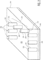
- FIG. 2 illustrates an embodiment of a printed circuit board 210 which, for example, may be in the first connector 12 of the cable 10.
- the printed circuit board 210 is electrically coupled to the chip for processing and or routing the signals between the mobile device 20 and the signal lines of the cable 10.
- the printed circuit board and chip may be included in a chip package coupled between a plug of the first connector 12 and the signal lines of the cable.
- the printed circuit board 210 includes a filter 250 formed from a plurality of ground pins 220 arranged in a predetermined pattern.
- the ground pins 220 are located in a respective plurality of vias 230 in the printed circuit board.
- Each ground pin 220 may include a first end 222 coupled to a common and/or all ground layers 240 and an opposing second end 224 coupled to the chip.
- the ground pins 220 may be arranged in a predetermined pattern.
- the ground pins 220 may at least partially surround (or otherwise be adjacent to) one or more signal conductors of the chip (e.g., located in area 275) to form a ring- or bracket-shaped RF shield for filtering out EMI generated by the one or more signal conductors.
- the ground pins 220 may be symmetrically arranged relative to the signal conductors of the chip in order to provide electrostatic discharge protection and to filter harmonics (e.g., third- and fourth-order harmonics) and other forms of RF noise generated by signals passing through the signal conductors. This symmetric arrangement may reduce de-sense in the electronic device 20, while at the same time reduce or minimize mixed mode conversion and adverse effects caused by ESD. This symmetric arrangement may also reduce the amount of losses across the signal path and may reduce harmful reflections due to insertion of the chip in the signal path.
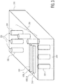
- FIG. 3 illustrates a pair of signal conductors 310 and 320 on the printed circuit board 210 of FIG. 2 .
- the signal conductors may be signal lines or conductive traces within or on a surface of the printed circuit board.
- the signal conductors 310 and 320 form a differential signal line that carries one or more USB high-speed signals (e.g., USB2.0, USB3.1 Gen1, USB3.1 Gen2, etc.) received from or transmitted through the cable 10.
- USB_N and USB_P indicating a differential signal line, where N stands for negative and P stands for positive.
- the signal conductors 310 and 320 may be coupled to the pinouts of the chip package (e.g., by bumps, etc.) to be mounted on the printed circuit board.
- the ground conductors 220 in the printed circuit board filter EMI generated when the USB signals pass through the signal lines.
- the ground conductors 220 are symmetrically arranged (e.g., in this case a U-shape or partial ring) relative to the signal lines.
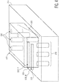
- FIG. 4 illustrates a chip located within a chip package (collectively labeled 410) mounted on the printed circuit board 210.
- the chip package includes pinout terminals (generally “pinouts") respectively connected to the USB signal lines (e.g., 310 and 320) and ground conductors 220 on the printed circuit board. While only two signal lines USB_N and USB_P are illustrated, it is understood that the printed circuit board 210 may include conductive lines for all of the pinouts of the chip package 410, in order to allow for an exchange of signals between the mobile device 20 and the peripheral device 30 through cable 10.
- the chip of the chip package 410 may include conductors (e.g., bumps, pinouts, contacts, etc.) electrically connected to respective ones of the pinouts of the chip package.
- FIG. 5 illustrates an embodiment of a chip 510 which may include a filter 550 that includes a plurality of ground conductors (GND) 520 and two USB differential signal lines.
- the first differential signal line includes a first signal line USB_Inp and a second signal line USB_Outp.
- the second differential signal line includes a first signal line USB_Inn and a second signal line USB_Outn.
- the ground conductors 520 are arranged in a symmetrical pattern surrounding both of the USB differential signal lines (in one embodiment, additional ground conductors could be provided so that the USB differential signal lines are fully surrounded).
- the ground conductors 520 therefore, form an RF shield around the signal lines to filter out harmonics, noise, and/or other forms of EMI that may contribute to the de-sense of the mobile device 20.
- the embodiment of FIG. 5 may also be used to represent a chip package 580, where GND 520 corresponds to ground pins (or pinouts), USB_Inp and USB_Outp correspond to signal pins (or pinouts) for the first differential signal line, and USB_Inn and USB_Outn correspond to signal pins (or pinouts) for the second differential signal line.
- the ground pins 520 are at least partially arranged in a ring or bracket (e.g., C-shaped) pattern around the USB signal pinouts of the chip package.
- FIG. 6 illustrates a differential pair of signal lines 610 and 620, which, for example, may correspond to the USB input line or output line.
- signal lines 610 and 620 are high-speed lines that are connected to respective pinouts, e.g., pinouts USB_Inn and USB_Inp as illustrated in FIG. 5 . At least portions of the signal lines 610 and 620 may be connected to the conductive traces USB_N and USB_P on the printed circuit board 210 illustrated in FIG. 3 .
- the pinouts and differential signals lines are electrically connected to USB switches 630 in the mobile device 20 illustrated in FIG. 1 .
- a clamp circuit 640 is coupled to the USB switches 630 through signal lines 650 and 660. Each of the signal lines 650 and 660 is coupled to a respective one of the pinouts through a diode circuit 670/680 to provide electrostatic discharge protection (ESD).
- ESD electrostatic discharge protection
- a symmetrical design which reduces or eliminates EMI emissions and mixed-mode conversions.
- This symmetrical design includes placing ESD diode circuits 670 and 680 and their associated conductive signal paths, and all associated layout including shield ring, ground network, and biasing power network, in a symmetrical pattern relative to the USB pinouts and signal lines.
- the size(s) and type(s) of diodes may be selected to produce a predetermined level of ESD performance, while reducing or minimizing de-sensing in USB communications at the same time.
- ESD diodes may be used with junction capacitances that are pre-biased at a (higher) voltage that minimizes equivalent junction capacitances at each pin, thereby improving return loss. This enhancement may benefit overall signal integrity performance of the USB signaling including de-sensing reduction or minimization.
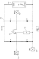
- FIG. 7 illustrates an equivalent circuit diagram of the ESD protection features of FIG. 6 for a USB signal path, and more particularly includes an embodiment of a switch structure for USB communications.
- Any asymmetry in the metal routing relative to the pad-opening, ESD diodes, clamp circuit, and USB switch block may adversely affect common mode-to-differential rejection ratio, which, in turn, may increase mismatch in capacitive coupling between the USB P/N pins.
- the conductive lines and metal routings are symmetrically arranged relative to the USB P/N signal switch 710.
- the switch 710 may include, for example, an n-type MOSFET which is coupled between pins 721 and 722.
- Pin 721 may be a pin on the host circuit/system side and pin 722 may be a pin (e.g., USB_P) pin of the cable side.
- the switch 710 is also connected to a ground pin 220 through a resistor 730.
- the gate voltage oft he transistor swich 710 may be generated by sensing the input common mode voltage, which is then level shifted to a higher voltage using a charge pump voltage. Each switch side is protected with the help of ESD diodes, and the resulting current is then discharged either through a ground plane or via floating ESD rail.
- the ESD protection features include diodes D1 and D2 coupled between an ESD rail 750 and the ground pin 220.
- the ESD rail 750 is coupled to the anode of an electrostatic discharge diode 760.
- the cathode of diode 760 is coupled to the ground pin 220.
- diodes D1 and D2 are forward biased, which, in turn, forward biases diode 760 to discharge electricity to ground.
- the diodes D1 and D2 and their associated lines are also symmetrically arranged. All of the symmetrical features of this arrangement may reduce, if not eliminate, the mismatch in capacitive coupling parasitics, which may reduce or minimize de-sense in the mobile device 20.
- FIGS. 8A to 11B illustrate simulated results for one or more embodiments.
- FIGS. 8A and 8B illustrate example results achieved by the filter and symmetrical arrangement of features achieved by one or more embodiments described herein. These results show the reduction of skew achieved between the P and N lines of a differential USB signal line, for example, as shown in FIG. 3 or FIG. 5 .
- the symmetrical pattern of ground pins of the filter produced a symmetry of the insertion loss between P & N signal pins between the die and package. Symmetry improvements are for both input and output sides of the chip. Results also show a significant reduction in the amount of insertion loss realized over a 10 GHz frequency range, compared with an arrangement which does not have the filter described herein.
- FIG. 8A illustrate example results achieved by the filter and symmetrical arrangement of features achieved by one or more embodiments described herein. These results show the reduction of skew achieved between the P and N lines of a differential USB signal line, for example, as shown in FIG. 3 or FIG. 5 .
- the symmetrical pattern of ground pins of the filter produced a symmetry of
- FIGS. 8C and 8D illustrate, in comparison, results obtained without the filter and symmetrical arrangement features in FIGS. 8A and 8B .
- the results show that skew, insertion loss, and return loss are much worse when the filter is not included in an asymmetrical arrangement.
- FIGS. 8C and 8D illustrate, in comparison, results obtained without the filter and symmetrical arrangement features in FIGS. 8A and 8B .
- the results show that skew, insertion loss, and return loss are much worse when the filter is not included in an asymmetrical arrangement.
- FIGS. 9A-9C illustrates example results of improved package and die performance relative to another arrangement that does not have the filter described herein.
- the lower curve showed that a filter in accordance with one or more embodiments produced lower differential return loss compared with the upper curve, which represents the performance of another tested arrangement.
- the upper curve showed that the filter produced an improved level of different insertion loss.
- the lower curve shows that the filter produced a significant reduction in capacitive coupling between the differential signal lines, compared to the upper curve corresponding to another arrangement that omitted the filter.
- FIGS. 10A and 10B illustrate example results of the improved mixed mode conversion performance of a chip/chip package that includes the filter described herein.
- FIG. 10A illustrates an example of common-to-differential mixed mode results
- FIG. 10B illustrates an example of differential-to-common mixed mode results. From these results, it is apparent that EMI and de-sense would be significantly reduced as a result of the filter described herein.
- FIGS. 10C and 10D illustrate, in comparison, results obtained without the chip/chip package of FIGS. 10A and 10B . These results show must worse mixed mod conversion performance.
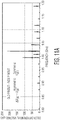
- FIGS. 11A and 11B illustrate examples of a reduction in harmonic emissions achieved out to the third- and fourth-orders from a chip including a filter as described herein. Reducing these harmonics produces a proportional reduction in EMI and de-sense, which, in turn, may improve the overall performance of the mobile device.
- the spacings, size, materials, and/or other feature of the ground conductors may be adjusted in order to tune the filter to operate in a specific frequency range and/or to suppress certain harmonics to reduce de-sense in the mobile device.
- a filter in accordance with one or more embodiments described herein eliminates the need to perform EMI filtering by an external chip or device. Also, in accordance with one or more embodiments, parasitic capacitance between adjacent signal lines, pins, conductors, etc., may be reduced, return loss may be improved in a way that suppresses unwanted RF emissions produced from mismatch, insertion loss may be improved, and mixed mode conversions may be reduced or minimized.
Landscapes
- Engineering & Computer Science (AREA)
- Microelectronics & Electronic Packaging (AREA)
- Physics & Mathematics (AREA)
- Electromagnetism (AREA)
- General Engineering & Computer Science (AREA)
- Theoretical Computer Science (AREA)
- Computer Hardware Design (AREA)
- General Physics & Mathematics (AREA)
- Shielding Devices Or Components To Electric Or Magnetic Fields (AREA)
Abstract
Description
- Example embodiments disclosed herein relate to filtering signals in an electronic circuit.
- Smart phones, tablets, and other mobile devices experience performance degradation for a variety of reasons. One reason is de-sense, e.g., the degradation in sensitivity that takes place in a mobile device as a result of electronic noise. The noise may come from many sources, including signals traveling through the lines of an interface such as a Universal Serial Bus (USB) cable. These signals may generate harmonics that interfere with (and thus degrade) receiver sensitivity and/or the signal quality of an antenna.
- In one case, the degradation in receiver sensitivity may occur from harmonics and/or other forms of noise adversely affecting a differential signal path. In another case, impedance mismatch may occur that generates noise. In either case, the noise is coupled to or picked up by the antenna of the mobile device. This problem is exacerbated the closer the antenna is to a semiconductor device (sometimes referred to as a "chip") generating or carrying the signals. All of these effects may ultimately distort the linearity of the receiver and/or reduce spurious-free dynamic range (SFDR), which, in turn, produces de-sense that reduces sensitivity.
- Various attempts have been made to reduce de-sense in a mobile device. One attempt involves adding an external chip to a cable connected between the USB port of the mobile device and the USB port of a connected peripheral device. However, such a chip may generate noise that makes the de-sense problem worse. Another attempt involves adding an external electromagnetic interference (EMI) filter to the chip or the device to reduce de-sense in an operating band of interest. However, such a filter increases costs, design complexity, and consumes space.
- A brief summary of various example embodiments is presented below. Some simplifications and omissions may be made in the following summary, which is intended to highlight and introduce some aspects of the various example embodiments, but not to limit the scope of the invention. Detailed descriptions of example embodiments adequate to allow those of ordinary skill in the art to make and use the inventive concepts will follow in later sections.
- In accordance with one or more embodiments, a chip includes at least one signal conductor and a filter including a plurality of ground conductors. The at least one signal conductor is configured to carry a signal that conforms to an interface protocol, and the plurality of ground conductors at least partially surround the at least one signal conductor on a same die. The plurality of ground conductors configured to filter electromagnetic interference generated by the signal to be carried by the at least one signal conductor. The electromagnetic interference may include harmonics generated by the signal to be carried by the at least one signal conductor.
- The at least one signal conductor may include a first signal conductor and a second signal conductor and wherein the first and second signal conductors correspond to a differential signal line of the interface protocol. The ground conductors may be arranged in a symmetrical pattern that reduces mixed mode conversion. The chip may be electrically connected between (a) one or more signal lines of an interface and (b) a plug or connector of the interface. The interface may be a cable, and the interface protocol may be a Universal Serial Bus (USB) protocol.
- In accordance with one or more other embodiments, a chip package includes at least one signal pin and a filter including a plurality of ground pins. The at least one signal pin is configured to carry a signal that conforms to an interface protocol, and the plurality of ground pins at least partially surround the at least one signal pin to filter electromagnetic interference generated by the signal to be carried by the at least one signal pin. The electromagnetic interference may include harmonics generated by the signal to be carried by the at least one signal pin.
- The at least one signal pin may include a first signal pin and a second signal pin and wherein the first and second signal pins correspond to a differential signal line of the interface protocol. The ground pins may be arranged in a symmetrical pattern that reduces mixed mode conversion. The chip package may be electrically connected between (a) one or more signal lines of an interface and (b) a plug or connector of the interface. The interface may be a cable, and the interface protocol may be a Universal Serial Bus (USB) protocol. The chip package may include an electrostatic discharge circuit electrically connected to one or more of the ground pins. The electrostatic discharge circuit may include a plurality of diodes arranged in a symmetric pattern relative to the at least one signal pin.
- In accordance with one or more other embodiments, a printed circuit board includes a plurality of vias, at least one signal line, and a plurality of ground conductors. The plurality of ground conductors are in respective ones of the vias and at least partially surround the at least one signal line, which is configured to carry a signal that conforms to an interface protocol. The plurality of ground conductors are configured to filter electromagnetic interference generated by the signal to be carried by the at least one signal line. The ground conductors may be arranged symmetrically relative to the at least one signal line.
- The printed circuit board may include an electrostatic discharge circuit electrically connected to one or more of the ground conductors. The electrostatic discharge circuit may include a plurality of diodes arranged in a symmetric pattern relative to the at least one signal line. The at least one signal line may include a first signal line and a second signal line and wherein the first and second signal lines correspond to a differential signal line. The printed circuit board may include a first conductive line and a second conductive line adjacent to the first conductive line, where the first conductive line electrically connects a first diode to a first ground conductor of the plurality of ground conductors and the second conductive line electrically connects a second diode the first ground conductor or a second ground conductor of the plurality of ground conductors. The first and second conductive lines and the first and second diodes may be arranged in a symmetrical pattern between the first signal line and the second signal line.
- Additional objects and features of the invention will be more readily apparent from the following detailed description and appended claims when taken in conjunction with the drawings. Although several example embodiments are illustrated and described, like reference numerals identify like parts in each of the figures, in which:
-
FIG. 1 illustrates an embodiment of an interface connecting two devices. -
FIG. 2 illustrates an embodiment of a printed circuit board which includes a filter. -
FIG. 3 illustrates the printed circuit board including a differential signal line. -
FIG. 4 illustrates a chip and chip package mounted on the printed circuit board. -
FIG. 5 illustrates an embodiment of a chip and chip package including a filter. -
FIG. 6 illustrates an embodiment including a symmetrical arrangement of features that reduce de-sense and perform electrostatic discharge protection. -
FIG. 7 illustrates another embodiment for performing electrostatic discharge protection. -
FIGS. 8A and 8B illustrate example results according to one or more embodiments. -
FIGS. 8C and 8D illustrate results obtained without the embodiment(s) inFIGS. 8A and 8B . -
FIGS. 9A-9C illustrate example results according to one or more embodiments. -
FIGS. 10A and 10B illustrate example results according to one or more embodiments. -
FIGS. 10C and 10D illustrate results without the embodiments inFIGS. 10A and 10B . -
FIGS. 11A and11B illustrate example results according to one or more embodiments. - It should be understood that the figures are merely schematic and are not drawn to scale. It should also be understood that the same reference numerals are used throughout the figures to indicate the same or similar parts.
- The descriptions and drawings illustrate the principles of various example embodiments. It will thus be appreciated that those skilled in the art will be able to devise various arrangements that, although not explicitly described or shown herein, embody the principles of the invention and are included within its scope. Furthermore, all examples recited herein are principally intended expressly to be for pedagogical purposes to aid the reader in understanding the principles of the invention and the concepts contributed by the inventor(s) to furthering the art and are to be construed as being without limitation to such specifically recited examples and conditions. Additionally, the term, "or," as used herein, refers to a non-exclusive or (i.e., and/or), unless otherwise indicated (e.g., "or else" or "or in the alternative"). Also, the various example embodiments described herein are not necessarily mutually exclusive, as some example embodiments can be combined with one or more other example embodiments to form new example embodiments. Descriptors such as "first," "second," "third," etc., are not meant to limit the order of elements discussed, are used to distinguish one element from the next, and are generally interchangeable. Values such as maximum or minimum may be predetermined and set to different values based on the application.
- Example embodiments describe a filter that reduces de-sense in a mobile device or other electronic system that is adversely affected by noise, and particularly radio frequency (RF) noise. The filter may be integrated into a chip, chip package, and/or printed circuit board having an interface, and which chip, chip package, and/or printed circuit board coupled to (e.g., a part of, or external to) the mobile device. In some implementations, the chip, chip package, and/or printed circuit board may process or route signals between the device and the signal lines of a cable. In this case, the filter may be located, for example, in a plug of the cable connecting the mobile device to another (e.g., peripheral) device. In one embodiment, the chip, chip package, and/or printed circuit board may be included in a communications port of the mobile device or connected device.
- Integrating the filter directly into the chip, chip package, or printed circuit board may reduce de-sense or other noise-related effects that may adversely affect performance of the mobile device. The integrated filter may also prevent an increase in costs that are incurred by other approaches and may also be implemented without consuming extra chip space or the use of external components. In one embodiment, the ground conductors of the filter may be used to perform electrostatic discharge (ESD) protection and/or a switching function that reduces corrosion.
-
FIG. 1 illustrates an embodiment of aninterface 10 used to connect anelectronic device 20 to another (e.g., peripheral)device 30. Theinterface 10 may be a cable, connector, or other communications path that includes one or more conductors for carrying signals, e.g., power, data, control, etc. For illustrative purposes, the interface will be discussed as acable 10 which includes afirst connector 12 and asecond connector 14. Thefirst connector 12 is coupled to (e.g., plugged into) a receptacle orport 22 of theelectronic device 20 and may include a chip, chip package, and/or printed circuit board in accordance with embodiments described herein. The chip may process and/or route signals between the signal lines in the cable and theelectronic device 20. Thesecond connector 14 is coupled to (e.g., plugged into) a receptacle orport 32 of theperipheral device 30. Examples of the cable include a USB (e.g., USB Type-C), FireWire, Thunderbolt, Display Port, PCIe, Lightning, and HDMI cable. - The
interface 10 includes a plurality of ground conductors that are distributed in a predetermined pattern around or adjacent to one or more signal conductors on the chip (e.g., die), chip package, and/or printed circuit board. The ground conductors may form a filter for electromagnetic interference (EMI) generated by signals carried by the one or more signal conductors. The conductors may be pins, signal lines, pads, traces, or other conductors for carrying signals. - In one embodiment, the filter is included in the chip to shield the
mobile device 10 from EMI generated by USB signals carried by a signal conductor. In this case, the ground conductors may at least partially surround the one or more signal conductors on a same die of the chip. In one embodiment, the filter is included in the chip package to shield themobile device 10 from EMI generated by USB signals carried by at least one signal pin. In this case, a plurality of ground pins may at least partially surround the at least one signal pin to filter EMI generated by the USB signals carried by the at least one signal pin. In one embodiment, the filter is included on a printed circuit board to which the chip and chip package are mounted. In this case, a plurality of ground conductors surround at least one signal line carrying USB signals. The ground conductors may be located in vias that enable connection of ground planes in the printed circuit board in order to filter EMI generated by the USB signals carried by the at least one signal line. In another embodiments, the filter (or portions thereof) may be included on all or a portion of the chip, chip package, and printed circuit board to form an RF shield for reducing EMI. - Such a filter may also be implemented to have a symmetrical arrangement of features that reduce the possibility of mixed-mode conversions from occurring, for example, as a result of connecting the chip (e.g., tapping or inline) to the
cable 10. In one or more embodiments, conductive lines and/or traces on the chip, package, and/or printed circuit board may be arranged in a symmetrical pattern along with electrostatic discharge features. - Through the self-integrated filtering operation performed by the ground conductors, performance of the
mobile device 10 may be improved through a reduction in de-sense. The ground conductors may also perform electrostatic discharge (ESD) protection and/or a switching function that reduces corrosion. Also, one or more embodiments may be implemented in a manner that does not increase costs, consume extra chip space, or require external components. - The
electronic device 20 may be any type of device that can be coupled to thecable 10, for example, for purposes of interacting with theelectronic device 10. In one embodiment, theelectronic device 20 may include an application processor which communicates with theperipheral device 30 through the chip, chip package, and/or printed circuit board in thefirst connector 12. Examples of theelectronic device 20 include a peripheral device, a smartphone, tablet, personal digital assistant, notebook or laptop computer, camera, navigation device, display, television, monitor, or another type of electronic device. For illustrative purposes, the electronic device will be discussed as a mobile device. - The
peripheral device 30 may be a notebook or laptop or desktop computer, charger, docking station, keyboard, speaker, adapter, portable hard drive, printer, scanner, or any other type of device designed to connect to and operate with an electronic device, for example, as described above. -
FIG. 2 illustrates an embodiment of a printedcircuit board 210 which, for example, may be in thefirst connector 12 of thecable 10. In one embodiment, the printedcircuit board 210 is electrically coupled to the chip for processing and or routing the signals between themobile device 20 and the signal lines of thecable 10. The printed circuit board and chip may be included in a chip package coupled between a plug of thefirst connector 12 and the signal lines of the cable. - Referring to
FIG. 2 , the printedcircuit board 210 includes afilter 250 formed from a plurality of ground pins 220 arranged in a predetermined pattern. The ground pins 220 are located in a respective plurality ofvias 230 in the printed circuit board. Eachground pin 220 may include afirst end 222 coupled to a common and/or all ground layers 240 and an opposingsecond end 224 coupled to the chip. The ground pins 220 may be arranged in a predetermined pattern. For example, the ground pins 220 may at least partially surround (or otherwise be adjacent to) one or more signal conductors of the chip (e.g., located in area 275) to form a ring- or bracket-shaped RF shield for filtering out EMI generated by the one or more signal conductors. In one embodiment, the ground pins 220 may be symmetrically arranged relative to the signal conductors of the chip in order to provide electrostatic discharge protection and to filter harmonics (e.g., third- and fourth-order harmonics) and other forms of RF noise generated by signals passing through the signal conductors. This symmetric arrangement may reduce de-sense in theelectronic device 20, while at the same time reduce or minimize mixed mode conversion and adverse effects caused by ESD. This symmetric arrangement may also reduce the amount of losses across the signal path and may reduce harmful reflections due to insertion of the chip in the signal path. -
FIG. 3 illustrates a pair ofsignal conductors circuit board 210 ofFIG. 2 . The signal conductors may be signal lines or conductive traces within or on a surface of the printed circuit board. In this example, thesignal conductors cable 10. For illustrative purposes, the signal conductors are labeled USB_N and USB_P indicating a differential signal line, where N stands for negative and P stands for positive. Thesignal conductors ground conductors 220 in the printed circuit board filter EMI generated when the USB signals pass through the signal lines. In one embodiment, theground conductors 220 are symmetrically arranged (e.g., in this case a U-shape or partial ring) relative to the signal lines. -
FIG. 4 illustrates a chip located within a chip package (collectively labeled 410) mounted on the printedcircuit board 210. The chip package includes pinout terminals (generally "pinouts") respectively connected to the USB signal lines (e.g., 310 and 320) andground conductors 220 on the printed circuit board. While only two signal lines USB_N and USB_P are illustrated, it is understood that the printedcircuit board 210 may include conductive lines for all of the pinouts of thechip package 410, in order to allow for an exchange of signals between themobile device 20 and theperipheral device 30 throughcable 10. The chip of thechip package 410 may include conductors (e.g., bumps, pinouts, contacts, etc.) electrically connected to respective ones of the pinouts of the chip package. -
FIG. 5 illustrates an embodiment of a chip 510 which may include afilter 550 that includes a plurality of ground conductors (GND) 520 and two USB differential signal lines. The first differential signal line includes a first signal line USB_Inp and a second signal line USB_Outp. The second differential signal line includes a first signal line USB_Inn and a second signal line USB_Outn. In this embodiment, theground conductors 520 are arranged in a symmetrical pattern surrounding both of the USB differential signal lines (in one embodiment, additional ground conductors could be provided so that the USB differential signal lines are fully surrounded). Theground conductors 520, therefore, form an RF shield around the signal lines to filter out harmonics, noise, and/or other forms of EMI that may contribute to the de-sense of themobile device 20. - The embodiment of
FIG. 5 may also be used to represent a chip package 580, whereGND 520 corresponds to ground pins (or pinouts), USB_Inp and USB_Outp correspond to signal pins (or pinouts) for the first differential signal line, and USB_Inn and USB_Outn correspond to signal pins (or pinouts) for the second differential signal line. As illustrated inFIG. 5 , the ground pins 520 are at least partially arranged in a ring or bracket (e.g., C-shaped) pattern around the USB signal pinouts of the chip package. -
FIG. 6 illustrates a differential pair ofsignal lines signal lines FIG. 5 . At least portions of thesignal lines circuit board 210 illustrated inFIG. 3 . The pinouts and differential signals lines are electrically connected toUSB switches 630 in themobile device 20 illustrated inFIG. 1 . Aclamp circuit 640 is coupled to the USB switches 630 throughsignal lines signal lines diode circuit 670/680 to provide electrostatic discharge protection (ESD). - In many designs, EMI emissions and mixed-mode conversions occur as a result of various factors including asymmetry. In accordance with one or more embodiments, a symmetrical design is presented which reduces or eliminates EMI emissions and mixed-mode conversions. This symmetrical design includes placing
ESD diode circuits -
FIG. 7 illustrates an equivalent circuit diagram of the ESD protection features ofFIG. 6 for a USB signal path, and more particularly includes an embodiment of a switch structure for USB communications. Any asymmetry in the metal routing relative to the pad-opening, ESD diodes, clamp circuit, and USB switch block may adversely affect common mode-to-differential rejection ratio, which, in turn, may increase mismatch in capacitive coupling between the USB P/N pins. - In the embodiment of
FIG. 7 , the conductive lines and metal routings are symmetrically arranged relative to the USB P/N signal switch 710. Theswitch 710 may include, for example, an n-type MOSFET which is coupled betweenpins Pin 721 may be a pin on the host circuit/system side and pin 722 may be a pin (e.g., USB_P) pin of the cable side. Theswitch 710 is also connected to aground pin 220 through aresistor 730. The gate voltage oft hetransistor swich 710 may be generated by sensing the input common mode voltage, which is then level shifted to a higher voltage using a charge pump voltage. Each switch side is protected with the help of ESD diodes, and the resulting current is then discharged either through a ground plane or via floating ESD rail. - The ESD protection features include diodes D1 and D2 coupled between an
ESD rail 750 and theground pin 220. TheESD rail 750 is coupled to the anode of anelectrostatic discharge diode 760. The cathode ofdiode 760 is coupled to theground pin 220. When an electrostatic discharge occurs, one or both of diodes D1 and D2 are forward biased, which, in turn,forward biases diode 760 to discharge electricity to ground. As shown inFIG. 7 , the diodes D1 and D2 and their associated lines are also symmetrically arranged. All of the symmetrical features of this arrangement may reduce, if not eliminate, the mismatch in capacitive coupling parasitics, which may reduce or minimize de-sense in themobile device 20. -
FIGS. 8A to 11B illustrate simulated results for one or more embodiments. -
FIGS. 8A and 8B illustrate example results achieved by the filter and symmetrical arrangement of features achieved by one or more embodiments described herein. These results show the reduction of skew achieved between the P and N lines of a differential USB signal line, for example, as shown inFIG. 3 orFIG. 5 . InFIG. 8A , the symmetrical pattern of ground pins of the filter produced a symmetry of the insertion loss between P & N signal pins between the die and package. Symmetry improvements are for both input and output sides of the chip. Results also show a significant reduction in the amount of insertion loss realized over a 10 GHz frequency range, compared with an arrangement which does not have the filter described herein. InFIG. 8B , the time delays associated with transmitting the USB signals was significantly lower as a result of the symmetrical ground pin arrangement.FIGS. 8C and 8D illustrate, in comparison, results obtained without the filter and symmetrical arrangement features inFIGS. 8A and 8B . The results show that skew, insertion loss, and return loss are much worse when the filter is not included in an asymmetrical arrangement.FIGS. 8C and 8D illustrate, in comparison, results obtained without the filter and symmetrical arrangement features inFIGS. 8A and 8B . The results show that skew, insertion loss, and return loss are much worse when the filter is not included in an asymmetrical arrangement. -
FIGS. 9A-9C illustrates example results of improved package and die performance relative to another arrangement that does not have the filter described herein. InFIG. 9A , the lower curve showed that a filter in accordance with one or more embodiments produced lower differential return loss compared with the upper curve, which represents the performance of another tested arrangement. InFIG. 9B , the upper curve showed that the filter produced an improved level of different insertion loss. InFIG. 9C , the lower curve shows that the filter produced a significant reduction in capacitive coupling between the differential signal lines, compared to the upper curve corresponding to another arrangement that omitted the filter. -
FIGS. 10A and 10B illustrate example results of the improved mixed mode conversion performance of a chip/chip package that includes the filter described herein.FIG. 10A illustrates an example of common-to-differential mixed mode results, andFIG. 10B illustrates an example of differential-to-common mixed mode results. From these results, it is apparent that EMI and de-sense would be significantly reduced as a result of the filter described herein.FIGS. 10C and 10D illustrate, in comparison, results obtained without the chip/chip package ofFIGS. 10A and 10B . These results show must worse mixed mod conversion performance. -
FIGS. 11A and11B illustrate examples of a reduction in harmonic emissions achieved out to the third- and fourth-orders from a chip including a filter as described herein. Reducing these harmonics produces a proportional reduction in EMI and de-sense, which, in turn, may improve the overall performance of the mobile device. In one embodiment, the spacings, size, materials, and/or other feature of the ground conductors may be adjusted in order to tune the filter to operate in a specific frequency range and/or to suppress certain harmonics to reduce de-sense in the mobile device. - As all of the example results show, a filter in accordance with one or more embodiments described herein eliminates the need to perform EMI filtering by an external chip or device. Also, in accordance with one or more embodiments, parasitic capacitance between adjacent signal lines, pins, conductors, etc., may be reduced, return loss may be improved in a way that suppresses unwanted RF emissions produced from mismatch, insertion loss may be improved, and mixed mode conversions may be reduced or minimized.
- Although the various exemplary embodiments have been described in detail with particular reference to certain exemplary aspects thereof, it should be understood that the invention is capable of other example embodiments and its details are capable of modifications in various obvious respects. As is readily apparent to those skilled in the art, variations and modifications can be affected while remaining within the spirit and scope of the invention. By way of non-limiting example, the specification speaks of a semiconductor device such as a chip, and it will be appreciated that the invention can apply to a semiconductor device that is a single chip, as well as a semiconductor device that includes multiple chips, such as a multi-chip module. Accordingly, the foregoing disclosure, description, and figures are for illustrative purposes only and do not in any way limit the invention, which is defined only by the claims.
Claims (15)
- A chip, comprising:at least one signal conductor; anda filter including a plurality of ground conductors,wherein the at least one signal conductor is configured to carry a signal that conforms to an interface protocol and wherein the plurality of ground conductors at least partially surround the at least one signal conductor on a same die, the plurality of ground conductors to filter electromagnetic interference generated by the signal to be carried by the at least one signal conductor.
- The chip of claim 1, wherein the electromagnetic interference includes harmonics generated by the signal to be carried by the at least one signal conductor.
- The chip of claim 1 or 2, wherein the at least one signal conductor includes a first signal conductor and a second signal conductor and wherein the first and second signal conductors correspond to a differential signal line of the interface protocol.
- The chip of any preceding claim, wherein the ground conductors are arranged in a symmetrical pattern that reduces mixed mode conversion.
- The chip of any preceding claim, wherein the chip is electrically connected (a) between one or more signal lines of an interface and (b) a plug or connector of the interface.
- The chip of claim 5, wherein the interface is a cable.
- The chip of any preceding claim, wherein the interface protocol is a Universal Serial Bus (USB) protocol.
- A chip package, comprising:at least one signal pin; anda filter including a plurality of ground pins,wherein the at least one signal pin is configured to carry a signal that conforms to an interface protocol and wherein the plurality of ground pins at least partially surround the at least one signal pin, the plurality of ground pins configured to filter electromagnetic interference generated by the signal to be carried by the at least one signal pin.
- The chip package of claim 8, wherein the electromagnetic interference includes harmonics generated by the signal to be carried by the at least one signal pin.
- The chip package of claim 8 or 9, wherein the at least one signal pin includes a first signal pin and a second signal pin and wherein the first and second signal pins correspond to a differential signal line of the interface protocol.
- The chip package of any preceding claim, wherein the ground pins are arranged in a symmetrical pattern that reduces mixed mode conversion.
- The chip package of any preceding claim, wherein the chip package is electrically connected between one or more signal lines of an interface and a plug or connector of the interface.
- The chip package of claim 12, wherein the interface is a cable.
- The chip package of any of claims 8 to 13, wherein the interface protocol is a Universal Serial Bus (USB) protocol.
- The chip package of any of claims 8 to 14, further comprising:
an electrostatic discharge circuit electrically connected to one or more of the ground pins, wherein the electrostatic discharge circuit includes a plurality of diodes arranged in a symmetric pattern relative to the at least one signal pin.
Applications Claiming Priority (1)
| Application Number | Priority Date | Filing Date | Title |
|---|---|---|---|
| US16/397,709 US11457524B2 (en) | 2019-04-29 | 2019-04-29 | Integrated filter for de-sense reduction |
Publications (2)
| Publication Number | Publication Date |
|---|---|
| EP3734464A1 true EP3734464A1 (en) | 2020-11-04 |
| EP3734464B1 EP3734464B1 (en) | 2022-06-22 |
Family
ID=70333860
Family Applications (1)
| Application Number | Title | Priority Date | Filing Date |
|---|---|---|---|
| EP20170341.0A Active EP3734464B1 (en) | 2019-04-29 | 2020-04-20 | Integrated filter for de-sense reduction |
Country Status (3)
| Country | Link |
|---|---|
| US (1) | US11457524B2 (en) |
| EP (1) | EP3734464B1 (en) |
| CN (1) | CN111864318B (en) |
Families Citing this family (1)
| Publication number | Priority date | Publication date | Assignee | Title |
|---|---|---|---|---|
| US11810875B2 (en) | 2021-04-09 | 2023-11-07 | Nxp B.V. | Packaged integrated circuit device with built-in baluns |
Citations (7)
| Publication number | Priority date | Publication date | Assignee | Title |
|---|---|---|---|---|
| US20070188997A1 (en) * | 2006-02-14 | 2007-08-16 | Sun Microsystems, Inc. | Interconnect design for reducing radiated emissions |
| US20090207538A1 (en) * | 2008-02-14 | 2009-08-20 | Akros Silicon Inc. | Electrostatic discharge protection circuit |
| US20140185249A1 (en) * | 2012-12-28 | 2014-07-03 | Sercomm Corporation | Wireless module |
| US20160021735A1 (en) * | 2014-07-17 | 2016-01-21 | Via Technologies, Inc. | Through-hole layout structure, circuit board, and electronic assembly |
| WO2018227324A1 (en) * | 2017-06-12 | 2018-12-20 | Qualcomm Incorporated | Flexible printed circuits for usb 3.0 interconnects in mobile devices |
| US10236938B2 (en) * | 2008-12-23 | 2019-03-19 | Keyssa, Inc. | Contactless replacement for cabled standards-based interfaces |
| TW201944664A (en) * | 2018-04-13 | 2019-11-16 | 岱煒科技股份有限公司 | USB A female connector can breakthrough problems of interference caused by resonance generated from radio frequency |
Family Cites Families (40)
| Publication number | Priority date | Publication date | Assignee | Title |
|---|---|---|---|---|
| JPH0637202A (en) * | 1992-07-20 | 1994-02-10 | Mitsubishi Electric Corp | Microwave IC package |
| US5912597A (en) * | 1994-03-31 | 1999-06-15 | Canon Kabushiki Kaisha | Printed circuit board |
| JP3631343B2 (en) * | 1995-12-04 | 2005-03-23 | 富士通株式会社 | Communication / information terminal equipment |
| US6097581A (en) * | 1997-04-08 | 2000-08-01 | X2Y Attenuators, Llc | Paired multi-layered dielectric independent passive component architecture resulting in differential and common mode filtering with surge protection in one integrated package |
| JP4078804B2 (en) * | 1998-01-19 | 2008-04-23 | エックストゥーワイ アテニュエイターズ,エル.エル.シー. | Paired multi-layer dielectric independent passive component architecture with integrated package and differential common mode filter with surge protection |
| US6936917B2 (en) * | 2001-09-26 | 2005-08-30 | Molex Incorporated | Power delivery connector for integrated circuits utilizing integrated capacitors |
| US7443693B2 (en) * | 2003-04-15 | 2008-10-28 | Wavezero, Inc. | Electromagnetic interference shielding for a printed circuit board |
| KR100583458B1 (en) * | 2004-01-28 | 2006-05-26 | 삼성전자주식회사 | Printed Circuit Boards Considering EMI |
| US7615856B2 (en) * | 2004-09-01 | 2009-11-10 | Sanyo Electric Co., Ltd. | Integrated antenna type circuit apparatus |
| KR100601704B1 (en) * | 2004-10-04 | 2006-07-18 | 삼성전자주식회사 | Method for reducing EMI and circuit connecting apparatus therefor |
| US7522883B2 (en) * | 2004-12-14 | 2009-04-21 | Quellan, Inc. | Method and system for reducing signal interference |
| CN2791727Y (en) * | 2005-02-01 | 2006-06-28 | 上海环达计算机科技有限公司 | Circuit board and host board using same |
| JP5084153B2 (en) * | 2005-08-15 | 2012-11-28 | キヤノン株式会社 | Printed board |
| US7479680B2 (en) * | 2005-11-30 | 2009-01-20 | California Micro Devices | Method and apparatus that provides differential connections with improved ESD protection and routing |
| KR100818473B1 (en) * | 2006-09-05 | 2008-04-01 | 삼성전기주식회사 | Electromagnetic shielding and charge discharge prevention printed circuit board device |
| CN101415317B (en) * | 2007-10-18 | 2011-07-06 | 英业达股份有限公司 | Anti-electromagnetic interference structure of multilayer printed circuit board |
| JP2009135213A (en) * | 2007-11-29 | 2009-06-18 | Mitsubishi Electric Corp | Printed wiring board |
| US11147977B2 (en) * | 2008-03-20 | 2021-10-19 | Greatbatch Ltd. | MLCC filter on an aimd circuit board conductively connected to a ground pin attached to a hermetic feedthrough ferrule |
| KR101030990B1 (en) * | 2008-12-31 | 2011-04-22 | 삼성에스디아이 주식회사 | Semiconductor package and plasma display device having same |
| JP5585092B2 (en) * | 2009-10-22 | 2014-09-10 | ソニー株式会社 | Wireless transmission system, wireless communication device |
| JP5593714B2 (en) * | 2010-01-29 | 2014-09-24 | 富士通株式会社 | Electronic element shield structure and electronic device equipped with the same |
| KR101855294B1 (en) * | 2010-06-10 | 2018-05-08 | 삼성전자주식회사 | Semiconductor package |
| CN102683311B (en) * | 2011-03-10 | 2014-12-10 | 精材科技股份有限公司 | Chip package and method of forming the same |
| WO2012144228A1 (en) * | 2011-04-21 | 2012-10-26 | 株式会社村田製作所 | Circuit module |
| TWI444115B (en) * | 2012-03-12 | 2014-07-01 | Mediatek Inc | Printed circuit board and chip system |
| CN106233634A (en) * | 2014-04-16 | 2016-12-14 | 莱尼电缆控股有限公司 | For differential data signals being carried out equipment and the method for signal transmission |
| US9369165B1 (en) | 2014-06-13 | 2016-06-14 | Amazon Technologies, Inc. | Mitigating desense in collocated speaker and antenna system |
| WO2016052125A1 (en) * | 2014-09-30 | 2016-04-07 | 株式会社村田製作所 | Transmission line member and electronic apparatus |
| WO2017006553A1 (en) * | 2015-07-08 | 2017-01-12 | 日本電気株式会社 | Printed wiring board |
| TWI535341B (en) * | 2015-07-30 | 2016-05-21 | Giga Byte Tech Co Ltd | Reduce the structure of electromagnetic interference and reduce the electromagnetic interference method |
| US9960747B2 (en) * | 2016-02-29 | 2018-05-01 | Skyworks Solutions, Inc. | Integrated filter and directional coupler assemblies |
| US9793661B2 (en) * | 2016-03-18 | 2017-10-17 | Tektronix, Inc. | Differential pin to RF adaptor for probing applications |
| US9634774B1 (en) | 2016-06-06 | 2017-04-25 | Motorola Mobility Llc | Desense reduction via pin remap in modular device |
| US9799947B1 (en) | 2016-06-06 | 2017-10-24 | Motorola Mobility Llc | Modular device system desense reduction |
| US9780755B1 (en) | 2016-09-16 | 2017-10-03 | Apple Inc. | On flex circuit desense filter for wireless communications |
| DE102016225727B4 (en) * | 2016-12-21 | 2025-04-17 | Vitesco Technologies Germany Gmbh | ESD-optimized control unit design concept |
| CN108463048B (en) * | 2017-02-21 | 2022-04-15 | 拉碧斯半导体株式会社 | Substrate circuit device |
| JP6950400B2 (en) * | 2017-09-22 | 2021-10-13 | 住友電気工業株式会社 | Mach Zenda Modulator |
| WO2020031872A1 (en) * | 2018-08-06 | 2020-02-13 | 株式会社村田製作所 | Circuit board, circuit board module, and antenna module |
| US20210399925A1 (en) * | 2020-06-17 | 2021-12-23 | Realtek Semiconductor Corp. | Signal transmission device capable of transmitting multiple data streams |
-
2019
- 2019-04-29 US US16/397,709 patent/US11457524B2/en active Active
-
2020
- 2020-04-14 CN CN202010293017.6A patent/CN111864318B/en active Active
- 2020-04-20 EP EP20170341.0A patent/EP3734464B1/en active Active
Patent Citations (7)
| Publication number | Priority date | Publication date | Assignee | Title |
|---|---|---|---|---|
| US20070188997A1 (en) * | 2006-02-14 | 2007-08-16 | Sun Microsystems, Inc. | Interconnect design for reducing radiated emissions |
| US20090207538A1 (en) * | 2008-02-14 | 2009-08-20 | Akros Silicon Inc. | Electrostatic discharge protection circuit |
| US10236938B2 (en) * | 2008-12-23 | 2019-03-19 | Keyssa, Inc. | Contactless replacement for cabled standards-based interfaces |
| US20140185249A1 (en) * | 2012-12-28 | 2014-07-03 | Sercomm Corporation | Wireless module |
| US20160021735A1 (en) * | 2014-07-17 | 2016-01-21 | Via Technologies, Inc. | Through-hole layout structure, circuit board, and electronic assembly |
| WO2018227324A1 (en) * | 2017-06-12 | 2018-12-20 | Qualcomm Incorporated | Flexible printed circuits for usb 3.0 interconnects in mobile devices |
| TW201944664A (en) * | 2018-04-13 | 2019-11-16 | 岱煒科技股份有限公司 | USB A female connector can breakthrough problems of interference caused by resonance generated from radio frequency |
Also Published As
| Publication number | Publication date |
|---|---|
| CN111864318A (en) | 2020-10-30 |
| US11457524B2 (en) | 2022-09-27 |
| CN111864318B (en) | 2023-11-17 |
| US20200344872A1 (en) | 2020-10-29 |
| EP3734464B1 (en) | 2022-06-22 |
Similar Documents
| Publication | Publication Date | Title |
|---|---|---|
| CA2754937C (en) | Circuits, systems and methods for implementing high speed data communications connectors that provide for reduced modal alien crosstalk in communications systems | |
| JP5050986B2 (en) | Communications system | |
| US20160276759A1 (en) | Cable connector | |
| US20150373827A1 (en) | Chip Heat Dissipation Structure and Terminal Device | |
| US11296499B2 (en) | Discharge protection circuit and method for operating a discharge protection circuit | |
| US11121507B2 (en) | Electrical connector with the tail segment of the second terminal of the shielding plate and the tail segments of the first terminals arranged in a same row | |
| EP3734464B1 (en) | Integrated filter for de-sense reduction | |
| CN112153182B (en) | Audio circuit and mobile terminal with same | |
| CN106601733A (en) | Circuit and packaging structure having electro-static discharge protecting function between radio frequency ground and analog ground | |
| US20210083489A1 (en) | Charging circuit and charging method | |
| US6578103B1 (en) | Compact PCI backplane and method of data transfer across the compact PCI backplane | |
| TWI408844B (en) | A communication device and a motherboard thereof | |
| US9705556B2 (en) | Differential capacitive antenna ports coexistence in wireless capacitive signal reception and transmission systems and/or wireless capacitive power supply transmission systems | |
| US20190044286A1 (en) | Ground bar as a robust grounding scheme for a high-speed connector design | |
| CN103579830B (en) | Interface module and method for reducing noise | |
| US12057671B2 (en) | Port processing method for ESD and EOS protection | |
| US7017001B2 (en) | Compact PCI backplane and method of data transfer across the compact PCI backplane | |
| KR102835504B1 (en) | Radio-frequency arrangement having two interconnected radio-frequency components | |
| CN103944021A (en) | Micro Secure Digital Adapter | |
| US10530078B1 (en) | Electronic signal processing device | |
| US6984132B1 (en) | Electrical connector semiconductor package with fly-over signal paths | |
| US20240006350A1 (en) | Semiconductor package, base station, mobile device and method for forming a semiconductor package | |
| US9356397B2 (en) | Connector and electronic system using the same | |
| US20240128947A1 (en) | In-phase noise suppression device | |
| CN110534980B (en) | High frequency optimized connector |
Legal Events
| Date | Code | Title | Description |
|---|---|---|---|
| PUAI | Public reference made under article 153(3) epc to a published international application that has entered the european phase |
Free format text: ORIGINAL CODE: 0009012 |
|
| STAA | Information on the status of an ep patent application or granted ep patent |
Free format text: STATUS: THE APPLICATION HAS BEEN PUBLISHED |
|
| AK | Designated contracting states |
Kind code of ref document: A1 Designated state(s): AL AT BE BG CH CY CZ DE DK EE ES FI FR GB GR HR HU IE IS IT LI LT LU LV MC MK MT NL NO PL PT RO RS SE SI SK SM TR |
|
| AX | Request for extension of the european patent |
Extension state: BA ME |
|
| STAA | Information on the status of an ep patent application or granted ep patent |
Free format text: STATUS: REQUEST FOR EXAMINATION WAS MADE |
|
| 17P | Request for examination filed |
Effective date: 20210504 |
|
| RBV | Designated contracting states (corrected) |
Designated state(s): AL AT BE BG CH CY CZ DE DK EE ES FI FR GB GR HR HU IE IS IT LI LT LU LV MC MK MT NL NO PL PT RO RS SE SI SK SM TR |
|
| GRAP | Despatch of communication of intention to grant a patent |
Free format text: ORIGINAL CODE: EPIDOSNIGR1 |
|
| STAA | Information on the status of an ep patent application or granted ep patent |
Free format text: STATUS: GRANT OF PATENT IS INTENDED |
|
| INTG | Intention to grant announced |
Effective date: 20220328 |
|
| GRAS | Grant fee paid |
Free format text: ORIGINAL CODE: EPIDOSNIGR3 |
|
| GRAA | (expected) grant |
Free format text: ORIGINAL CODE: 0009210 |
|
| STAA | Information on the status of an ep patent application or granted ep patent |
Free format text: STATUS: THE PATENT HAS BEEN GRANTED |
|
| AK | Designated contracting states |
Kind code of ref document: B1 Designated state(s): AL AT BE BG CH CY CZ DE DK EE ES FI FR GB GR HR HU IE IS IT LI LT LU LV MC MK MT NL NO PL PT RO RS SE SI SK SM TR |
|
| REG | Reference to a national code |
Ref country code: GB Ref legal event code: FG4D |
|
| REG | Reference to a national code |
Ref country code: CH Ref legal event code: EP |
|
| REG | Reference to a national code |
Ref country code: DE Ref legal event code: R096 Ref document number: 602020003616 Country of ref document: DE |
|
| REG | Reference to a national code |
Ref country code: AT Ref legal event code: REF Ref document number: 1500231 Country of ref document: AT Kind code of ref document: T Effective date: 20220715 |
|
| REG | Reference to a national code |
Ref country code: IE Ref legal event code: FG4D |
|
| REG | Reference to a national code |
Ref country code: LT Ref legal event code: MG9D |
|
| REG | Reference to a national code |
Ref country code: NL Ref legal event code: MP Effective date: 20220622 |
|
| PG25 | Lapsed in a contracting state [announced via postgrant information from national office to epo] |
Ref country code: SE Free format text: LAPSE BECAUSE OF FAILURE TO SUBMIT A TRANSLATION OF THE DESCRIPTION OR TO PAY THE FEE WITHIN THE PRESCRIBED TIME-LIMIT Effective date: 20220622 Ref country code: NO Free format text: LAPSE BECAUSE OF FAILURE TO SUBMIT A TRANSLATION OF THE DESCRIPTION OR TO PAY THE FEE WITHIN THE PRESCRIBED TIME-LIMIT Effective date: 20220922 Ref country code: LT Free format text: LAPSE BECAUSE OF FAILURE TO SUBMIT A TRANSLATION OF THE DESCRIPTION OR TO PAY THE FEE WITHIN THE PRESCRIBED TIME-LIMIT Effective date: 20220622 Ref country code: HR Free format text: LAPSE BECAUSE OF FAILURE TO SUBMIT A TRANSLATION OF THE DESCRIPTION OR TO PAY THE FEE WITHIN THE PRESCRIBED TIME-LIMIT Effective date: 20220622 Ref country code: GR Free format text: LAPSE BECAUSE OF FAILURE TO SUBMIT A TRANSLATION OF THE DESCRIPTION OR TO PAY THE FEE WITHIN THE PRESCRIBED TIME-LIMIT Effective date: 20220923 Ref country code: FI Free format text: LAPSE BECAUSE OF FAILURE TO SUBMIT A TRANSLATION OF THE DESCRIPTION OR TO PAY THE FEE WITHIN THE PRESCRIBED TIME-LIMIT Effective date: 20220622 Ref country code: BG Free format text: LAPSE BECAUSE OF FAILURE TO SUBMIT A TRANSLATION OF THE DESCRIPTION OR TO PAY THE FEE WITHIN THE PRESCRIBED TIME-LIMIT Effective date: 20220922 |
|
| REG | Reference to a national code |
Ref country code: AT Ref legal event code: MK05 Ref document number: 1500231 Country of ref document: AT Kind code of ref document: T Effective date: 20220622 |
|
| PG25 | Lapsed in a contracting state [announced via postgrant information from national office to epo] |
Ref country code: RS Free format text: LAPSE BECAUSE OF FAILURE TO SUBMIT A TRANSLATION OF THE DESCRIPTION OR TO PAY THE FEE WITHIN THE PRESCRIBED TIME-LIMIT Effective date: 20220622 Ref country code: LV Free format text: LAPSE BECAUSE OF FAILURE TO SUBMIT A TRANSLATION OF THE DESCRIPTION OR TO PAY THE FEE WITHIN THE PRESCRIBED TIME-LIMIT Effective date: 20220622 |
|
| PG25 | Lapsed in a contracting state [announced via postgrant information from national office to epo] |
Ref country code: NL Free format text: LAPSE BECAUSE OF FAILURE TO SUBMIT A TRANSLATION OF THE DESCRIPTION OR TO PAY THE FEE WITHIN THE PRESCRIBED TIME-LIMIT Effective date: 20220622 |
|
| PG25 | Lapsed in a contracting state [announced via postgrant information from national office to epo] |
Ref country code: SM Free format text: LAPSE BECAUSE OF FAILURE TO SUBMIT A TRANSLATION OF THE DESCRIPTION OR TO PAY THE FEE WITHIN THE PRESCRIBED TIME-LIMIT Effective date: 20220622 Ref country code: SK Free format text: LAPSE BECAUSE OF FAILURE TO SUBMIT A TRANSLATION OF THE DESCRIPTION OR TO PAY THE FEE WITHIN THE PRESCRIBED TIME-LIMIT Effective date: 20220622 Ref country code: RO Free format text: LAPSE BECAUSE OF FAILURE TO SUBMIT A TRANSLATION OF THE DESCRIPTION OR TO PAY THE FEE WITHIN THE PRESCRIBED TIME-LIMIT Effective date: 20220622 Ref country code: PT Free format text: LAPSE BECAUSE OF FAILURE TO SUBMIT A TRANSLATION OF THE DESCRIPTION OR TO PAY THE FEE WITHIN THE PRESCRIBED TIME-LIMIT Effective date: 20221024 Ref country code: ES Free format text: LAPSE BECAUSE OF FAILURE TO SUBMIT A TRANSLATION OF THE DESCRIPTION OR TO PAY THE FEE WITHIN THE PRESCRIBED TIME-LIMIT Effective date: 20220622 Ref country code: EE Free format text: LAPSE BECAUSE OF FAILURE TO SUBMIT A TRANSLATION OF THE DESCRIPTION OR TO PAY THE FEE WITHIN THE PRESCRIBED TIME-LIMIT Effective date: 20220622 Ref country code: CZ Free format text: LAPSE BECAUSE OF FAILURE TO SUBMIT A TRANSLATION OF THE DESCRIPTION OR TO PAY THE FEE WITHIN THE PRESCRIBED TIME-LIMIT Effective date: 20220622 Ref country code: AT Free format text: LAPSE BECAUSE OF FAILURE TO SUBMIT A TRANSLATION OF THE DESCRIPTION OR TO PAY THE FEE WITHIN THE PRESCRIBED TIME-LIMIT Effective date: 20220622 |
|
| PG25 | Lapsed in a contracting state [announced via postgrant information from national office to epo] |
Ref country code: PL Free format text: LAPSE BECAUSE OF FAILURE TO SUBMIT A TRANSLATION OF THE DESCRIPTION OR TO PAY THE FEE WITHIN THE PRESCRIBED TIME-LIMIT Effective date: 20220622 Ref country code: IS Free format text: LAPSE BECAUSE OF FAILURE TO SUBMIT A TRANSLATION OF THE DESCRIPTION OR TO PAY THE FEE WITHIN THE PRESCRIBED TIME-LIMIT Effective date: 20221022 |
|
| REG | Reference to a national code |
Ref country code: DE Ref legal event code: R097 Ref document number: 602020003616 Country of ref document: DE |
|
| PG25 | Lapsed in a contracting state [announced via postgrant information from national office to epo] |
Ref country code: AL Free format text: LAPSE BECAUSE OF FAILURE TO SUBMIT A TRANSLATION OF THE DESCRIPTION OR TO PAY THE FEE WITHIN THE PRESCRIBED TIME-LIMIT Effective date: 20220622 |
|
| PG25 | Lapsed in a contracting state [announced via postgrant information from national office to epo] |
Ref country code: DK Free format text: LAPSE BECAUSE OF FAILURE TO SUBMIT A TRANSLATION OF THE DESCRIPTION OR TO PAY THE FEE WITHIN THE PRESCRIBED TIME-LIMIT Effective date: 20220622 |
|
| PLBE | No opposition filed within time limit |
Free format text: ORIGINAL CODE: 0009261 |
|
| STAA | Information on the status of an ep patent application or granted ep patent |
Free format text: STATUS: NO OPPOSITION FILED WITHIN TIME LIMIT |
|
| 26N | No opposition filed |
Effective date: 20230323 |
|
| P01 | Opt-out of the competence of the unified patent court (upc) registered |
Effective date: 20230725 |
|
| PG25 | Lapsed in a contracting state [announced via postgrant information from national office to epo] |
Ref country code: SI Free format text: LAPSE BECAUSE OF FAILURE TO SUBMIT A TRANSLATION OF THE DESCRIPTION OR TO PAY THE FEE WITHIN THE PRESCRIBED TIME-LIMIT Effective date: 20220622 |
|
| REG | Reference to a national code |
Ref country code: CH Ref legal event code: PL |
|
| PG25 | Lapsed in a contracting state [announced via postgrant information from national office to epo] |
Ref country code: LU Free format text: LAPSE BECAUSE OF NON-PAYMENT OF DUE FEES Effective date: 20230420 |
|
| REG | Reference to a national code |
Ref country code: BE Ref legal event code: MM Effective date: 20230430 |
|
| PG25 | Lapsed in a contracting state [announced via postgrant information from national office to epo] |
Ref country code: MC Free format text: LAPSE BECAUSE OF FAILURE TO SUBMIT A TRANSLATION OF THE DESCRIPTION OR TO PAY THE FEE WITHIN THE PRESCRIBED TIME-LIMIT Effective date: 20220622 |
|
| PG25 | Lapsed in a contracting state [announced via postgrant information from national office to epo] |
Ref country code: MC Free format text: LAPSE BECAUSE OF FAILURE TO SUBMIT A TRANSLATION OF THE DESCRIPTION OR TO PAY THE FEE WITHIN THE PRESCRIBED TIME-LIMIT Effective date: 20220622 Ref country code: LI Free format text: LAPSE BECAUSE OF NON-PAYMENT OF DUE FEES Effective date: 20230430 Ref country code: IT Free format text: LAPSE BECAUSE OF FAILURE TO SUBMIT A TRANSLATION OF THE DESCRIPTION OR TO PAY THE FEE WITHIN THE PRESCRIBED TIME-LIMIT Effective date: 20220622 Ref country code: FR Free format text: LAPSE BECAUSE OF NON-PAYMENT OF DUE FEES Effective date: 20230430 Ref country code: CH Free format text: LAPSE BECAUSE OF NON-PAYMENT OF DUE FEES Effective date: 20230430 |
|
| REG | Reference to a national code |
Ref country code: IE Ref legal event code: MM4A |
|
| PG25 | Lapsed in a contracting state [announced via postgrant information from national office to epo] |
Ref country code: BE Free format text: LAPSE BECAUSE OF NON-PAYMENT OF DUE FEES Effective date: 20230430 |
|
| PG25 | Lapsed in a contracting state [announced via postgrant information from national office to epo] |
Ref country code: IE Free format text: LAPSE BECAUSE OF NON-PAYMENT OF DUE FEES Effective date: 20230420 |
|
| PG25 | Lapsed in a contracting state [announced via postgrant information from national office to epo] |
Ref country code: IE Free format text: LAPSE BECAUSE OF NON-PAYMENT OF DUE FEES Effective date: 20230420 |
|
| PG25 | Lapsed in a contracting state [announced via postgrant information from national office to epo] |
Ref country code: BG Free format text: LAPSE BECAUSE OF FAILURE TO SUBMIT A TRANSLATION OF THE DESCRIPTION OR TO PAY THE FEE WITHIN THE PRESCRIBED TIME-LIMIT Effective date: 20220622 |
|
| PG25 | Lapsed in a contracting state [announced via postgrant information from national office to epo] |
Ref country code: BG Free format text: LAPSE BECAUSE OF FAILURE TO SUBMIT A TRANSLATION OF THE DESCRIPTION OR TO PAY THE FEE WITHIN THE PRESCRIBED TIME-LIMIT Effective date: 20220622 |
|
| GBPC | Gb: european patent ceased through non-payment of renewal fee |
Effective date: 20240420 |
|
| PG25 | Lapsed in a contracting state [announced via postgrant information from national office to epo] |
Ref country code: GB Free format text: LAPSE BECAUSE OF NON-PAYMENT OF DUE FEES Effective date: 20240420 |
|
| PG25 | Lapsed in a contracting state [announced via postgrant information from national office to epo] |
Ref country code: GB Free format text: LAPSE BECAUSE OF NON-PAYMENT OF DUE FEES Effective date: 20240420 |
|
| PGFP | Annual fee paid to national office [announced via postgrant information from national office to epo] |
Ref country code: DE Payment date: 20250319 Year of fee payment: 6 |
|
| PG25 | Lapsed in a contracting state [announced via postgrant information from national office to epo] |
Ref country code: CY Free format text: LAPSE BECAUSE OF FAILURE TO SUBMIT A TRANSLATION OF THE DESCRIPTION OR TO PAY THE FEE WITHIN THE PRESCRIBED TIME-LIMIT; INVALID AB INITIO Effective date: 20200420 |
|
| PG25 | Lapsed in a contracting state [announced via postgrant information from national office to epo] |
Ref country code: HU Free format text: LAPSE BECAUSE OF FAILURE TO SUBMIT A TRANSLATION OF THE DESCRIPTION OR TO PAY THE FEE WITHIN THE PRESCRIBED TIME-LIMIT; INVALID AB INITIO Effective date: 20200420 |
|
| PG25 | Lapsed in a contracting state [announced via postgrant information from national office to epo] |
Ref country code: TR Free format text: LAPSE BECAUSE OF FAILURE TO SUBMIT A TRANSLATION OF THE DESCRIPTION OR TO PAY THE FEE WITHIN THE PRESCRIBED TIME-LIMIT Effective date: 20220622 |