EP3734321A1 - Wave guide transition for radar chip package - Google Patents
Wave guide transition for radar chip package Download PDFInfo
- Publication number
- EP3734321A1 EP3734321A1 EP20166797.9A EP20166797A EP3734321A1 EP 3734321 A1 EP3734321 A1 EP 3734321A1 EP 20166797 A EP20166797 A EP 20166797A EP 3734321 A1 EP3734321 A1 EP 3734321A1
- Authority
- EP
- European Patent Office
- Prior art keywords
- transitions
- transceiver
- waveguides
- air
- electrical channels
- Prior art date
- Legal status (The legal status is an assumption and is not a legal conclusion. Google has not performed a legal analysis and makes no representation as to the accuracy of the status listed.)
- Granted
Links
Images


Classifications
-
- H—ELECTRICITY
- H01—ELECTRIC ELEMENTS
- H01P—WAVEGUIDES; RESONATORS, LINES, OR OTHER DEVICES OF THE WAVEGUIDE TYPE
- H01P3/00—Waveguides; Transmission lines of the waveguide type
- H01P3/12—Hollow waveguides
- H01P3/121—Hollow waveguides integrated in a substrate
-
- G—PHYSICS
- G01—MEASURING; TESTING
- G01S—RADIO DIRECTION-FINDING; RADIO NAVIGATION; DETERMINING DISTANCE OR VELOCITY BY USE OF RADIO WAVES; LOCATING OR PRESENCE-DETECTING BY USE OF THE REFLECTION OR RERADIATION OF RADIO WAVES; ANALOGOUS ARRANGEMENTS USING OTHER WAVES
- G01S7/00—Details of systems according to groups G01S13/00, G01S15/00, G01S17/00
- G01S7/48—Details of systems according to groups G01S13/00, G01S15/00, G01S17/00 of systems according to group G01S17/00
- G01S7/483—Details of pulse systems
- G01S7/484—Transmitters
-
- G—PHYSICS
- G01—MEASURING; TESTING
- G01S—RADIO DIRECTION-FINDING; RADIO NAVIGATION; DETERMINING DISTANCE OR VELOCITY BY USE OF RADIO WAVES; LOCATING OR PRESENCE-DETECTING BY USE OF THE REFLECTION OR RERADIATION OF RADIO WAVES; ANALOGOUS ARRANGEMENTS USING OTHER WAVES
- G01S7/00—Details of systems according to groups G01S13/00, G01S15/00, G01S17/00
- G01S7/02—Details of systems according to groups G01S13/00, G01S15/00, G01S17/00 of systems according to group G01S13/00
- G01S7/03—Details of HF subsystems specially adapted therefor, e.g. common to transmitter and receiver
- G01S7/032—Constructional details for solid-state radar subsystems
-
- H—ELECTRICITY
- H01—ELECTRIC ELEMENTS
- H01P—WAVEGUIDES; RESONATORS, LINES, OR OTHER DEVICES OF THE WAVEGUIDE TYPE
- H01P5/00—Coupling devices of the waveguide type
- H01P5/08—Coupling devices of the waveguide type for linking dissimilar lines or devices
- H01P5/10—Coupling devices of the waveguide type for linking dissimilar lines or devices for coupling balanced lines or devices with unbalanced lines or devices
- H01P5/107—Hollow-waveguide/strip-line transitions
-
- H—ELECTRICITY
- H01—ELECTRIC ELEMENTS
- H01Q—ANTENNAS, i.e. RADIO AERIALS
- H01Q1/00—Details of, or arrangements associated with, antennas
- H01Q1/12—Supports; Mounting means
- H01Q1/22—Supports; Mounting means by structural association with other equipment or articles
- H01Q1/2283—Supports; Mounting means by structural association with other equipment or articles mounted in or on the surface of a semiconductor substrate as a chip-type antenna or integrated with other components into an IC package
-
- H—ELECTRICITY
- H01—ELECTRIC ELEMENTS
- H01Q—ANTENNAS, i.e. RADIO AERIALS
- H01Q1/00—Details of, or arrangements associated with, antennas
- H01Q1/27—Adaptation for use in or on movable bodies
- H01Q1/32—Adaptation for use in or on road or rail vehicles
- H01Q1/3208—Adaptation for use in or on road or rail vehicles characterised by the application wherein the antenna is used
- H01Q1/3233—Adaptation for use in or on road or rail vehicles characterised by the application wherein the antenna is used particular used as part of a sensor or in a security system, e.g. for automotive radar, navigation systems
-
- H—ELECTRICITY
- H01—ELECTRIC ELEMENTS
- H01Q—ANTENNAS, i.e. RADIO AERIALS
- H01Q1/00—Details of, or arrangements associated with, antennas
- H01Q1/36—Structural form of radiating elements, e.g. cone, spiral, umbrella; Particular materials used therewith
- H01Q1/38—Structural form of radiating elements, e.g. cone, spiral, umbrella; Particular materials used therewith formed by a conductive layer on an insulating support
-
- H—ELECTRICITY
- H01—ELECTRIC ELEMENTS
- H01Q—ANTENNAS, i.e. RADIO AERIALS
- H01Q1/00—Details of, or arrangements associated with, antennas
- H01Q1/50—Structural association of antennas with earthing switches, lead-in devices or lightning protectors
-
- H—ELECTRICITY
- H01—ELECTRIC ELEMENTS
- H01Q—ANTENNAS, i.e. RADIO AERIALS
- H01Q21/00—Antenna arrays or systems
- H01Q21/0006—Particular feeding systems
- H01Q21/0037—Particular feeding systems linear waveguide fed arrays
- H01Q21/0043—Slotted waveguides
-
- H—ELECTRICITY
- H01—ELECTRIC ELEMENTS
- H01Q—ANTENNAS, i.e. RADIO AERIALS
- H01Q7/00—Loop antennas with a substantially uniform current distribution around the loop and having a directional radiation pattern in a plane perpendicular to the plane of the loop
-
- H—ELECTRICITY
- H01—ELECTRIC ELEMENTS
- H01Q—ANTENNAS, i.e. RADIO AERIALS
- H01Q9/00—Electrically-short antennas having dimensions not more than twice the operating wavelength and consisting of conductive active radiating elements
- H01Q9/04—Resonant antennas
- H01Q9/0407—Substantially flat resonant element parallel to ground plane, e.g. patch antenna
- H01Q9/045—Substantially flat resonant element parallel to ground plane, e.g. patch antenna with particular feeding means
-
- H—ELECTRICITY
- H01—ELECTRIC ELEMENTS
- H01Q—ANTENNAS, i.e. RADIO AERIALS
- H01Q9/00—Electrically-short antennas having dimensions not more than twice the operating wavelength and consisting of conductive active radiating elements
- H01Q9/04—Resonant antennas
- H01Q9/16—Resonant antennas with feed intermediate between the extremities of the antenna, e.g. centre-fed dipole
-
- H—ELECTRICITY
- H10—SEMICONDUCTOR DEVICES; ELECTRIC SOLID-STATE DEVICES NOT OTHERWISE PROVIDED FOR
- H10W—GENERIC PACKAGES, INTERCONNECTIONS, CONNECTORS OR OTHER CONSTRUCTIONAL DETAILS OF DEVICES COVERED BY CLASS H10
- H10W44/00—Electrical arrangements for controlling or matching impedance
- H10W44/20—Electrical arrangements for controlling or matching impedance at high-frequency [HF] or radio frequency [RF]
-
- H—ELECTRICITY
- H10—SEMICONDUCTOR DEVICES; ELECTRIC SOLID-STATE DEVICES NOT OTHERWISE PROVIDED FOR
- H10W—GENERIC PACKAGES, INTERCONNECTIONS, CONNECTORS OR OTHER CONSTRUCTIONAL DETAILS OF DEVICES COVERED BY CLASS H10
- H10W44/00—Electrical arrangements for controlling or matching impedance
- H10W44/20—Electrical arrangements for controlling or matching impedance at high-frequency [HF] or radio frequency [RF]
- H10W44/203—Electrical connections
- H10W44/216—Waveguides, e.g. strip lines
-
- H—ELECTRICITY
- H10—SEMICONDUCTOR DEVICES; ELECTRIC SOLID-STATE DEVICES NOT OTHERWISE PROVIDED FOR
- H10W—GENERIC PACKAGES, INTERCONNECTIONS, CONNECTORS OR OTHER CONSTRUCTIONAL DETAILS OF DEVICES COVERED BY CLASS H10
- H10W44/00—Electrical arrangements for controlling or matching impedance
- H10W44/20—Electrical arrangements for controlling or matching impedance at high-frequency [HF] or radio frequency [RF]
- H10W44/241—Electrical arrangements for controlling or matching impedance at high-frequency [HF] or radio frequency [RF] for passive devices or passive elements
- H10W44/248—Electrical arrangements for controlling or matching impedance at high-frequency [HF] or radio frequency [RF] for passive devices or passive elements for antennas
-
- H—ELECTRICITY
- H10—SEMICONDUCTOR DEVICES; ELECTRIC SOLID-STATE DEVICES NOT OTHERWISE PROVIDED FOR
- H10W—GENERIC PACKAGES, INTERCONNECTIONS, CONNECTORS OR OTHER CONSTRUCTIONAL DETAILS OF DEVICES COVERED BY CLASS H10
- H10W72/00—Interconnections or connectors in packages
- H10W72/20—Bump connectors, e.g. solder bumps or copper pillars; Dummy bumps; Thermal bumps
- H10W72/241—Dispositions, e.g. layouts
-
- H—ELECTRICITY
- H10—SEMICONDUCTOR DEVICES; ELECTRIC SOLID-STATE DEVICES NOT OTHERWISE PROVIDED FOR
- H10W—GENERIC PACKAGES, INTERCONNECTIONS, CONNECTORS OR OTHER CONSTRUCTIONAL DETAILS OF DEVICES COVERED BY CLASS H10
- H10W90/00—Package configurations
- H10W90/701—Package configurations characterised by the relative positions of pads or connectors relative to package parts
- H10W90/721—Package configurations characterised by the relative positions of pads or connectors relative to package parts of bump connectors
- H10W90/724—Package configurations characterised by the relative positions of pads or connectors relative to package parts of bump connectors between a chip and a stacked insulating package substrate, interposer or RDL
Definitions
- This disclosure generally relates to a wave guide launcher for millimeter wave radar.
- the typical radar assembly includes a printed circuit board (PCB) placed between radar chip packages and radar waveguides to facilitate connections between the devices.
- PCB printed circuit board
- the PCB introduces electrical losses that reduce a range of transmission and a range of reception of the radar signals.
- a transceiver comprising a first plurality of electrical channels configured to transfer first electromagnetic signals to a first plurality of air waveguides; wherein each of the first plurality of electrical channels extend from an output of at least one transmitter along an exterior surface of a chip package that supports the at least one transmitter and terminate at first transitions disposed on the exterior surface; wherein the each of the first plurality of air waveguides are attached to the exterior surface and overlay one of the first transitions.
- Fig. 1 is an illustration of a transceiver 10 configured to transmit and receive electromagnetic signals.
- the transceiver 10 transmits and receives the electromagnetic signals in a 76GHz to 81GHz frequency band, such as those used in automotive radar systems.
- the transceiver 10 includes a chip package 12 including a die 13 including at least one transmitter 14 and at least one receiver 16.
- the at least one transmitter 14 and at least one receiver 16 transmit and receive the electromagnetic signals (i.e., the radar signals) through antennas 18 (see Fig. 4 ) in communication with the chip package 12.
- the chip package 12 is a monolithic microwave integrated circuit (MMIC) having a ball grid array (BGA) of interconnects (not shown) on an exterior surface 20.
- the chip package 12 supports three transmitters 14 and four receivers 16. It will be appreciated that the chip package 12 may support any number of transmitters 14 and receivers 16 within the dimensional limits of the chip package 12.
- Air waveguides 22 are placed between the chip package 12 and the antennas 18 to transport the radar signals being transmitted and received.
- the air waveguide 22 is a hollow metal structure that is capable of directing electromagnetic power from one area to another area.
- the transceiver 10 is an improvement over other transceivers, because the transceiver 10 eliminates an intermediate printed circuit board (PCB) that may be placed between chip packages and waveguides to facilitate connections between the devices.
- PCB printed circuit board
- the PCB introduces electrical losses that reduce a range of transmission and a range of reception of the radar signals.
- inclusion of the PCB results in added material and manufacturing costs.
- the transceiver 10 includes a first plurality of electrical channels 24 (i.e., signal transmission lines) configured to transfer first electromagnetic signals to a first plurality of air waveguides 22A.
- the first electromagnetic signals are the transmitted radar signals
- the air waveguides 22 are WR10 air waveguides 22.
- WR10 designates that the waveguide is rectangular, with the dimensions of 2.54mm by 1.27mm. Slight variations of these dimensions does not significantly deteriorate the performance of the waveguide, and the rectangular shape need not be a "perfect" rectangle.
- the dimensions of the air waveguide 22 establish a limit on a frequency of the electromagnetic signal that may be passed through the air waveguide 22.
- the air waveguides 22 may be formed with a tortuous path (i.e., bends) to direct the radar signals to and from the antennas 18 that may be arranged in an antenna array.
- Each of the first plurality of electrical channels 24 extend from outputs of at least one transmitter 14 along the exterior surface 20 of the chip package 12. That is, the first plurality of electrical channels 24 run along an outside of the chip package 12 and are exposed to the environment (e.g., air). In some configurations, this exposure results in about half of the guiding power propagating into the exterior surface 20, and about half of the guiding power propagating in the air. Because air has nearly no loss, this configuration ensures low transmission line losses.
- the first plurality of electrical channels 24 terminate at first transitions 26 disposed on the exterior surface 20.
- the first transitions 26 are a link between the transmission lines and the air waveguides 22, and will be described in more detail below.
- Each of the first plurality of air waveguides 22A are attached to the exterior surface 20 of the chip package 12 and overlay one of the first transitions 26.
- the first plurality of air waveguides 22A are integrated into a waveguide antenna assembly that is attached to the exterior surface 20 of the chip package 12.
- ends of the first plurality of air waveguides 22A are arranged within a surface of the waveguide antenna assembly to overlay the first transitions 26.
- the ends of the first plurality of air waveguides 22A that overlay the first transitions 26 may be open, or may be partially closed (e.g., slotted), as will be described in more detail below.
- the transceiver 10 also includes a second plurality of electrical channels 28 configured to transfer second electromagnetic signals from a second plurality of air waveguides 22B.
- the second electromagnetic signals are the received radar signals (i.e. the radar signals reflected from a target), and the air waveguides 22 are the WR10 air waveguides 22.
- Each of the second plurality of electrical channels 28 extend from an input of at least one receiver 16 along the exterior surface 20 of the chip package 12.
- the second plurality of electrical channels 28 terminate at second transitions 30 disposed on the exterior surface 20.
- Each of the second plurality of air waveguides 22B are attached to the exterior surface 20 and overlay one of the second transitions 30.
- the second plurality of air waveguides 22B are integrated into the waveguide antenna assembly that is attached to the exterior surface 20 of the chip package 12.
- ends of the second plurality of air waveguides 22B are arranged within the surface of the waveguide antenna assembly to overlay the second transitions 30.
- the ends of the second plurality of air waveguides 22B that overlay the second transitions 30 may be open, or may be partially closed (e.g., slotted), as will be described in more detail below.
- Figs. 2A-2C illustrate examples of the first plurality of electrical channels 24 and/or the second plurality of electrical channels 28 that include differential pairs of microstrips 32.
- the differential pair of microstrips 32 are formed of two, parallel metallic strips having a constant spacing along their length. One of the metallic strips is connected to a positive terminal of the respective transceiver 10 channel, and the other metallic strip is connected to a negative terminal of the respective transceiver 10 channel.
- the microstrips 32 are formed of metals, such as copper, aluminum, silver, gold, and alloys thereof, and may be formed on the exterior surface 20 by any of the known methods of deposition, such as physical vapor deposition.
- the microstrips 32 may be separated using techniques such as photolithography and/or micromachining.
- the differential pairs of microstrips 32 terminate in a region of the exterior surface 20 of the chip package 12 that is surrounded by a solder ball fence 33.
- One end of the solder ball fence 33 defines a gap (i.e., a "mouse hole") through which the differential pairs of microstrips 32 pass.
- the solder ball fence 33 provides electromagnetic shielding for the air waveguides 22.
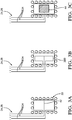
- Figs. 3A-3C illustrate examples of the first plurality of electrical channels 24 and the second plurality of electrical channels 28 that include co-planar waveguides 34.
- the co-planar waveguides 34 are formed of three, parallel, metallic strips having a constant spacing along their length. A center metallic strip is connected with a positive terminal of the respective transceiver 10 channel, and the other two metallic strips are attached to a negative terminal of the respective transceiver 10 channel.
- the co-planar waveguides 34 are formed of metals, such as copper, aluminum, silver, gold, and alloys thereof, and may be applied to the exterior surface 20 by any of the known methods of deposition, such as physical vapor deposition.
- the co-planar waveguides 34 may be separated using techniques such as photolithography and/or micromachining.
- the co-planar waveguides 34 also terminate in a region of the exterior surface 20 of the chip package 12 that is surrounded by the solder ball fence 33.
- One side of the solder ball fence 33 defines the gap through which the co-planar waveguides 34 pass.
- the co-planar waveguides 34 are arranged so that a 90-degree turn is made before passing through the gap, which assists in the conversion of the electromagnetic signals from the co-planar waveguides 34 to the air waveguides 22. That is, the 90-degree bend aligns a polarization of the co-planar waveguide 34 with the air waveguide 22 for maximum transition efficiency.
- the first plurality of electrical channels 24 and the second plurality of electrical channels 28 are of the same design (i.e., all differential pairs of microstrips 32 or all co-planar waveguides 34). In another example, the first plurality of electrical channels 24 and the second plurality of electrical channels 28 are of different designs. In an example, the first plurality of electrical channels 24 and the second plurality of electrical channels 28 terminate at first transitions 26 and second transitions 30 that are of the same design. In another example, the first plurality of electrical channels 24 and the second plurality of electrical channels 28 terminate at first transitions 26 and second transitions 30 that are of a different design.
- the following descriptions of the first plurality of electrical channels 28, the first transitions 26, and the first plurality of air waveguides 22A will also apply to the second plurality of electrical channels 28, the second transitions 30, and the second plurality of air waveguides 22B.
- Fig. 2A illustrates the differential pairs of microstrips 32 that terminate at the first transitions 26 which include a pair of opposed solder ball transitions 36.
- the pair of opposed solder ball transitions 36 may be formed of any solder alloy compatible with the chip package 12, such as alloys of silver and/or alloys of gold.
- the first plurality of air waveguides 22A include slotted air waveguides 22C where the slot is positioned between the pair of opposed solder ball transitions 36.
- the end of the slotted air waveguide 22C that overlays the pair of opposed solder ball transitions 36 is closed except for the slot.
- the pair of opposed solder ball transitions 36 are in electrical contact with the slotted end of the slotted air waveguide 22C.
- the slot is an opening in the end of the slotted air waveguide 22C and disrupts the electric and magnetic fields established between the solder balls. This disruption in the fields enables the radar signal to propagate along a particular axis through the slotted air waveguides 22C.
- Fig. 2B illustrates the differential pairs of microstrips 32 that terminate at the first transitions 26 which include loop transitions 38A.
- the loop transition 38A is continuous rectangular metallic loop that connects the differential pairs of microstrips 32.
- the loop transition 38A may be formed of metals, such as copper, aluminum, silver, gold, and alloys thereof.
- the end of the air waveguide 22A that overlays the loop transition 38A is open.
- the loop transition 38A has a perimeter equal to about one wavelength of the radar signal.
- the magnetic field surrounding the loop transition 38A created by the electrical current flow through the loop, generates the electromagnetic signal that is transported through the air waveguide 22A.
- Fig. 2C illustrates the differential pairs of microstrips 32 that terminate at the first transitions 26 which include bowtie transitions 40.
- the bowtie transitions 40 may be formed of metals, such as copper, aluminum, silver, gold, and alloys thereof.
- the bowtie transitions 40 are triangular metal pads that are in contact with the differential pairs of microstrips 32.
- the end of the air waveguide 22A that overlays the bowtie transition 40 is open.
- An angle between the opposing triangular metal pads of the bowtie transitions 40 specifies the frequency bandwidth of this first transition 26, as opposed to a perimeter dimension.
- the bowtie transition 40 is capable of operating in a wider range of frequencies, compared to the loop transition 38A.
- Fig. 3A illustrates the co-planar waveguides 34 that terminate at the first transitions 26 which include monopole transitions 42.
- the monopole transitions 42 are formed by extensions of the co-planar waveguides 34 into the region overlaid by the end of the air waveguide 22.
- the monopole transitions 42 may be formed of metals, such as copper, aluminum, silver, gold, and alloys thereof.
- the end of the air waveguide 22A that overlays the monopole transitions 42 is open.
- the length of the positive strip (i.e. the monopole) that extends into the region overlaid by the air waveguide 22 is equal to about one quarter of the wavelength of the radar signal.
- the two negative strips on either side of the monopole form a ground plane.
- the magnetic field surrounding the monopole transitions 42 created by a voltage potential between the monopole and the ground plane, generates the electromagnetic signal that is transported through the air waveguide 22A.
- Fig. 3B illustrates the co-planar waveguides 34 that terminate at the first transitions 26 which include loop transitions 38B.
- the loop transition 38B includes a continuous rectangular metallic loop that connects the two negative strips of the co-planar waveguide 34, and is bifurcated by the positive strip of the co-planar waveguides 34, creating two loops with equal perimeters.
- the loop transition 38B may be formed of metals, such as copper, aluminum, silver, gold, and alloys thereof.
- the end of the air waveguide 22A that overlays the loop transition 38B is open.
- Each of the two loops in the loop transition 38B has a perimeter of about one half of a wavelength of the radar signal.
- the magnetic field surrounding the loop transition 38B, created by the electrical current flow through the two loops, generates the electromagnetic signal that is transported through the air waveguide 22A.
- Fig. 3C illustrates the co-planar waveguides 34 that terminate at the first transitions 26 which include patch transitions 44.
- the patch transitions 44 may be formed of metals, such as copper, aluminum, silver, gold, and alloys thereof.
- the end of the air waveguide 22A that overlays the patch transitions 44 is open.
- the patch transitions 44 are rectangular metal pads that are in contact with the positive strip of the co-planar waveguides 34.
- the two negative strips form the ground plane.
- a length of the patch transitions 44 is about one half of a wave length, and the patch transitions 44 radiate the electromagnetic energy into the air waveguide 22 similar to an antenna 18.
- the magnetic field surrounding the patch transitions 44 created by the voltage potential between the patch and the ground plane, generates the electromagnetic signal that is transported through the air waveguide 22A.
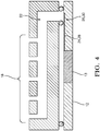
- Fig. 4 is a cross section view of the transceiver 10, illustrating an example of the antenna assembly that is attached to the exterior surface 20 of the chip package 12.
- the air waveguide 22 is integrated into the antenna assembly and directs the radar signals between the first transition 26 and the antennas 18.
- the antennas 18 are multiple slots that radiate and/or collect the radar signals.
- the antenna assembly is attached to the chip package 12 using solder balls from the BGA.
- first contact could be termed a second contact
- second contact could be termed a first contact
- the first contact and the second contact are both contacts, but they are not the same contact.
- the terminology used in the description of the various described embodiments herein is for the purpose of describing particular embodiments only and is not intended to be limiting. As used in the description of the various described embodiments and the appended claims, the singular forms "a”, “an” and “the” are intended to include the plural forms as well, unless the context clearly indicates otherwise. It will also be understood that the term “and/or” as used herein refers to and encompasses any and all possible combinations of one or more of the associated listed items.
- the phrase “if it is determined” or “if [a stated condition or event] is detected” is, optionally, construed to mean “upon determining” or “in response to determining” or “upon detecting [the stated condition or event]” or “in response to detecting [the stated condition or event],” depending on the context.
- Directional terms such as top, bottom, upper, lower, left, right, front, rear, etc. do not denote any particular orientation, but rather these directional terms are used to distinguish one element from another and establish a relationship between the various elements.
Landscapes
- Engineering & Computer Science (AREA)
- Radar, Positioning & Navigation (AREA)
- Remote Sensing (AREA)
- Microelectronics & Electronic Packaging (AREA)
- Computer Networks & Wireless Communication (AREA)
- Physics & Mathematics (AREA)
- General Physics & Mathematics (AREA)
- Computer Security & Cryptography (AREA)
- Radar Systems Or Details Thereof (AREA)
Abstract
Description
- This application claims the benefit of
U.S. Provisional Patent Application No. 62/839,904, filed April 29, 2019 - This disclosure generally relates to a wave guide launcher for millimeter wave radar.
- The typical radar assembly includes a printed circuit board (PCB) placed between radar chip packages and radar waveguides to facilitate connections between the devices. The PCB introduces electrical losses that reduce a range of transmission and a range of reception of the radar signals.
- This disclosure proposes to solve the above mentioned problem by providing a transceiver, comprising a first plurality of electrical channels configured to transfer first electromagnetic signals to a first plurality of air waveguides; wherein each of the first plurality of electrical channels extend from an output of at least one transmitter along an exterior surface of a chip package that supports the at least one transmitter and terminate at first transitions disposed on the exterior surface; wherein the each of the first plurality of air waveguides are attached to the exterior surface and overlay one of the first transitions.
- According to other advantageous features of the present invention:
- the transceiver further includes a second plurality of electrical channels configured to transfer second electromagnetic signals from a second plurality of air waveguides; wherein each of the second plurality of electrical channels extend from an input of at least one receiver along the exterior surface of the chip package that supports the at least one receiver and terminate at second transitions disposed on the exterior surface; wherein each of the second plurality of air waveguides are attached to the exterior surface and overlay one of the second transitions.
- the first plurality of electrical channels include differential pairs of microstrips;
- the first transitions include a pair of opposed solder ball transitions;
- the first plurality of air waveguides include slotted air waveguides;
- the first transitions include loop transitions;
- the first transitions include bowtie transitions;
- the first plurality of electrical channels include co-planar waveguides;
- the first transitions include monopole transitions;
- the first transitions include loop transitions;
- the first transitions include patch transitions;
- the second plurality of electrical channels include differential pairs of microstrips;
- the second transitions include a pair of opposed solder ball transitions;
- the second plurality of air waveguides include slotted air waveguides;
- the second transitions include loop transitions;
- the second transitions include bowtie transitions;
- the second plurality of electrical channels include co-planar waveguides;
- the second transitions include monopole transitions;
- the second transitions include loop transitions;
- the second transitions include patch transitions;
- the chip package includes at least four receivers;
- the chip package includes at least three transmitters.
- The present invention will now be described, by way of example with reference to the accompanying drawings, in which:
-
Fig. 1 is an illustration of transceiver in accordance with one embodiment; -
Fig. 2A is an illustration of electrical channels and transitions in accordance with one embodiment; -
Fig. 2B is an illustration of electrical channels and transitions in accordance with another embodiment; -
Fig. 2C is an illustration of electrical channels and transitions in accordance with yet another embodiment; -
Fig. 3A is an illustration of electrical channels and transitions in accordance with yet another embodiment; -
Fig. 3B is an illustration of electrical channels and transitions in accordance with yet another embodiment; -
Fig. 3C is an illustration of electrical channels and transitions in accordance with yet another embodiment; and -
Fig. 4 is a cross section of the transceiver ofFig. 1 in accordance with one embodiment. - Reference will now be made in detail to embodiments, examples of which are illustrated in the accompanying drawings. In the following detailed description, numerous specific details are set forth in order to provide a thorough understanding of the various described embodiments. However, it will be apparent to one of ordinary skill in the art that the various described embodiments may be practiced without these specific details. In other instances, well-known methods, procedures, components, circuits, and networks have not been described in detail so as not to unnecessarily obscure aspects of the embodiments.
-
Fig. 1 is an illustration of atransceiver 10 configured to transmit and receive electromagnetic signals. In an example, thetransceiver 10 transmits and receives the electromagnetic signals in a 76GHz to 81GHz frequency band, such as those used in automotive radar systems. Thetransceiver 10 includes achip package 12 including adie 13 including at least one transmitter 14 and at least onereceiver 16. The at least one transmitter 14 and at least onereceiver 16 transmit and receive the electromagnetic signals (i.e., the radar signals) through antennas 18 (seeFig. 4 ) in communication with thechip package 12. In the example illustrated inFig. 1 , thechip package 12 is a monolithic microwave integrated circuit (MMIC) having a ball grid array (BGA) of interconnects (not shown) on anexterior surface 20. In this example, thechip package 12 supports three transmitters 14 and fourreceivers 16. It will be appreciated that thechip package 12 may support any number of transmitters 14 andreceivers 16 within the dimensional limits of thechip package 12. -
Air waveguides 22 are placed between thechip package 12 and theantennas 18 to transport the radar signals being transmitted and received. Theair waveguide 22 is a hollow metal structure that is capable of directing electromagnetic power from one area to another area. Thetransceiver 10 is an improvement over other transceivers, because thetransceiver 10 eliminates an intermediate printed circuit board (PCB) that may be placed between chip packages and waveguides to facilitate connections between the devices. The PCB introduces electrical losses that reduce a range of transmission and a range of reception of the radar signals. In addition, inclusion of the PCB results in added material and manufacturing costs. - Referring back to
Fig. 1 , thetransceiver 10 includes a first plurality of electrical channels 24 (i.e., signal transmission lines) configured to transfer first electromagnetic signals to a first plurality ofair waveguides 22A. In the example illustrated inFig. 1 , the first electromagnetic signals are the transmitted radar signals, and theair waveguides 22 are WR10air waveguides 22. WR10 designates that the waveguide is rectangular, with the dimensions of 2.54mm by 1.27mm. Slight variations of these dimensions does not significantly deteriorate the performance of the waveguide, and the rectangular shape need not be a "perfect" rectangle. The dimensions of theair waveguide 22 establish a limit on a frequency of the electromagnetic signal that may be passed through theair waveguide 22. The air waveguides 22 may be formed with a tortuous path (i.e., bends) to direct the radar signals to and from theantennas 18 that may be arranged in an antenna array. - Each of the first plurality of
electrical channels 24 extend from outputs of at least one transmitter 14 along theexterior surface 20 of thechip package 12. That is, the first plurality ofelectrical channels 24 run along an outside of thechip package 12 and are exposed to the environment (e.g., air). In some configurations, this exposure results in about half of the guiding power propagating into theexterior surface 20, and about half of the guiding power propagating in the air. Because air has nearly no loss, this configuration ensures low transmission line losses. - The first plurality of
electrical channels 24 terminate atfirst transitions 26 disposed on theexterior surface 20. Thefirst transitions 26 are a link between the transmission lines and theair waveguides 22, and will be described in more detail below. Each of the first plurality ofair waveguides 22A are attached to theexterior surface 20 of thechip package 12 and overlay one of the first transitions 26. In an example, the first plurality ofair waveguides 22A are integrated into a waveguide antenna assembly that is attached to theexterior surface 20 of thechip package 12. In this example, ends of the first plurality ofair waveguides 22A are arranged within a surface of the waveguide antenna assembly to overlay the first transitions 26. The ends of the first plurality ofair waveguides 22A that overlay thefirst transitions 26 may be open, or may be partially closed (e.g., slotted), as will be described in more detail below. - The
transceiver 10 also includes a second plurality ofelectrical channels 28 configured to transfer second electromagnetic signals from a second plurality ofair waveguides 22B. In the example illustrated inFig. 1 , the second electromagnetic signals are the received radar signals (i.e. the radar signals reflected from a target), and theair waveguides 22 are theWR10 air waveguides 22. Each of the second plurality ofelectrical channels 28 extend from an input of at least onereceiver 16 along theexterior surface 20 of thechip package 12. The second plurality ofelectrical channels 28 terminate atsecond transitions 30 disposed on theexterior surface 20. Each of the second plurality ofair waveguides 22B are attached to theexterior surface 20 and overlay one of the second transitions 30. In an example, the second plurality ofair waveguides 22B are integrated into the waveguide antenna assembly that is attached to theexterior surface 20 of thechip package 12. In this example, ends of the second plurality ofair waveguides 22B are arranged within the surface of the waveguide antenna assembly to overlay the second transitions 30. The ends of the second plurality ofair waveguides 22B that overlay thesecond transitions 30 may be open, or may be partially closed (e.g., slotted), as will be described in more detail below. -
Figs. 2A-2C illustrate examples of the first plurality ofelectrical channels 24 and/or the second plurality ofelectrical channels 28 that include differential pairs ofmicrostrips 32. The differential pair ofmicrostrips 32 are formed of two, parallel metallic strips having a constant spacing along their length. One of the metallic strips is connected to a positive terminal of therespective transceiver 10 channel, and the other metallic strip is connected to a negative terminal of therespective transceiver 10 channel. Themicrostrips 32 are formed of metals, such as copper, aluminum, silver, gold, and alloys thereof, and may be formed on theexterior surface 20 by any of the known methods of deposition, such as physical vapor deposition. Themicrostrips 32 may be separated using techniques such as photolithography and/or micromachining. In the examples illustrates inFigs. 2A-2C , the differential pairs ofmicrostrips 32 terminate in a region of theexterior surface 20 of thechip package 12 that is surrounded by asolder ball fence 33. One end of thesolder ball fence 33 defines a gap (i.e., a "mouse hole") through which the differential pairs ofmicrostrips 32 pass. Thesolder ball fence 33 provides electromagnetic shielding for theair waveguides 22. -
Figs. 3A-3C illustrate examples of the first plurality ofelectrical channels 24 and the second plurality ofelectrical channels 28 that includeco-planar waveguides 34. Theco-planar waveguides 34 are formed of three, parallel, metallic strips having a constant spacing along their length. A center metallic strip is connected with a positive terminal of therespective transceiver 10 channel, and the other two metallic strips are attached to a negative terminal of therespective transceiver 10 channel. Theco-planar waveguides 34 are formed of metals, such as copper, aluminum, silver, gold, and alloys thereof, and may be applied to theexterior surface 20 by any of the known methods of deposition, such as physical vapor deposition. Theco-planar waveguides 34 may be separated using techniques such as photolithography and/or micromachining. In the examples illustrates inFigs. 3A-3C , theco-planar waveguides 34 also terminate in a region of theexterior surface 20 of thechip package 12 that is surrounded by thesolder ball fence 33. One side of thesolder ball fence 33 defines the gap through which theco-planar waveguides 34 pass. Theco-planar waveguides 34 are arranged so that a 90-degree turn is made before passing through the gap, which assists in the conversion of the electromagnetic signals from theco-planar waveguides 34 to theair waveguides 22. That is, the 90-degree bend aligns a polarization of theco-planar waveguide 34 with theair waveguide 22 for maximum transition efficiency. - In an example, the first plurality of
electrical channels 24 and the second plurality ofelectrical channels 28 are of the same design (i.e., all differential pairs ofmicrostrips 32 or all co-planar waveguides 34). In another example, the first plurality ofelectrical channels 24 and the second plurality ofelectrical channels 28 are of different designs. In an example, the first plurality ofelectrical channels 24 and the second plurality ofelectrical channels 28 terminate atfirst transitions 26 andsecond transitions 30 that are of the same design. In another example, the first plurality ofelectrical channels 24 and the second plurality ofelectrical channels 28 terminate atfirst transitions 26 andsecond transitions 30 that are of a different design. The following descriptions of the first plurality ofelectrical channels 28, thefirst transitions 26, and the first plurality ofair waveguides 22A will also apply to the second plurality ofelectrical channels 28, thesecond transitions 30, and the second plurality ofair waveguides 22B. -
Fig. 2A illustrates the differential pairs ofmicrostrips 32 that terminate at thefirst transitions 26 which include a pair of opposed solder ball transitions 36. The pair of opposed solder ball transitions 36 may be formed of any solder alloy compatible with thechip package 12, such as alloys of silver and/or alloys of gold. In this example, the first plurality ofair waveguides 22A include slottedair waveguides 22C where the slot is positioned between the pair of opposed solder ball transitions 36. In this example, the end of the slottedair waveguide 22C that overlays the pair of opposed solder ball transitions 36 is closed except for the slot. The pair of opposed solder ball transitions 36 are in electrical contact with the slotted end of the slottedair waveguide 22C. The slot is an opening in the end of the slottedair waveguide 22C and disrupts the electric and magnetic fields established between the solder balls. This disruption in the fields enables the radar signal to propagate along a particular axis through the slottedair waveguides 22C. -
Fig. 2B illustrates the differential pairs ofmicrostrips 32 that terminate at thefirst transitions 26 which includeloop transitions 38A. In this example, theloop transition 38A is continuous rectangular metallic loop that connects the differential pairs ofmicrostrips 32. Theloop transition 38A may be formed of metals, such as copper, aluminum, silver, gold, and alloys thereof. In this example, the end of theair waveguide 22A that overlays theloop transition 38A is open. Theloop transition 38A has a perimeter equal to about one wavelength of the radar signal. The magnetic field surrounding theloop transition 38A, created by the electrical current flow through the loop, generates the electromagnetic signal that is transported through theair waveguide 22A. -
Fig. 2C illustrates the differential pairs ofmicrostrips 32 that terminate at thefirst transitions 26 which include bowtie transitions 40. The bowtie transitions 40 may be formed of metals, such as copper, aluminum, silver, gold, and alloys thereof. In this example, the bowtie transitions 40 are triangular metal pads that are in contact with the differential pairs ofmicrostrips 32. In this example, the end of theair waveguide 22A that overlays thebowtie transition 40 is open. An angle between the opposing triangular metal pads of the bowtie transitions 40 specifies the frequency bandwidth of thisfirst transition 26, as opposed to a perimeter dimension. Thebowtie transition 40 is capable of operating in a wider range of frequencies, compared to theloop transition 38A. -
Fig. 3A illustrates theco-planar waveguides 34 that terminate at thefirst transitions 26 which include monopole transitions 42. The monopole transitions 42 are formed by extensions of theco-planar waveguides 34 into the region overlaid by the end of theair waveguide 22. The monopole transitions 42 may be formed of metals, such as copper, aluminum, silver, gold, and alloys thereof. In this example, the end of theair waveguide 22A that overlays the monopole transitions 42 is open. In this example, the length of the positive strip (i.e. the monopole) that extends into the region overlaid by theair waveguide 22 is equal to about one quarter of the wavelength of the radar signal. The two negative strips on either side of the monopole form a ground plane. The magnetic field surrounding the monopole transitions 42, created by a voltage potential between the monopole and the ground plane, generates the electromagnetic signal that is transported through theair waveguide 22A. -
Fig. 3B illustrates theco-planar waveguides 34 that terminate at thefirst transitions 26 which include loop transitions 38B. In this example, theloop transition 38B includes a continuous rectangular metallic loop that connects the two negative strips of theco-planar waveguide 34, and is bifurcated by the positive strip of theco-planar waveguides 34, creating two loops with equal perimeters. Theloop transition 38B may be formed of metals, such as copper, aluminum, silver, gold, and alloys thereof. In this example, the end of theair waveguide 22A that overlays theloop transition 38B is open. Each of the two loops in theloop transition 38B has a perimeter of about one half of a wavelength of the radar signal. The magnetic field surrounding theloop transition 38B, created by the electrical current flow through the two loops, generates the electromagnetic signal that is transported through theair waveguide 22A. -
Fig. 3C illustrates theco-planar waveguides 34 that terminate at thefirst transitions 26 which include patch transitions 44. The patch transitions 44 may be formed of metals, such as copper, aluminum, silver, gold, and alloys thereof. In this example, the end of theair waveguide 22A that overlays the patch transitions 44 is open. In this example, the patch transitions 44 are rectangular metal pads that are in contact with the positive strip of theco-planar waveguides 34. The two negative strips form the ground plane. A length of the patch transitions 44 is about one half of a wave length, and the patch transitions 44 radiate the electromagnetic energy into theair waveguide 22 similar to anantenna 18. The magnetic field surrounding the patch transitions 44, created by the voltage potential between the patch and the ground plane, generates the electromagnetic signal that is transported through theair waveguide 22A. -
Fig. 4 is a cross section view of thetransceiver 10, illustrating an example of the antenna assembly that is attached to theexterior surface 20 of thechip package 12. In this example, theair waveguide 22 is integrated into the antenna assembly and directs the radar signals between thefirst transition 26 and theantennas 18. In this example, theantennas 18 are multiple slots that radiate and/or collect the radar signals. In this example, the antenna assembly is attached to thechip package 12 using solder balls from the BGA. - While this invention has been described in terms of the preferred embodiments thereof, it is not intended to be so limited, but rather only to the extent set forth in the claims that follow. "One or more" includes a function being performed by one element, a function being performed by more than one element, e.g., in a distributed fashion, several functions being performed by one element, several functions being performed by several elements, or any combination of the above. It will also be understood that, although the terms first, second, etc. are, in some instances, used herein to describe various elements, these elements should not be limited by these terms. These terms are only used to distinguish one element from another. For example, a first contact could be termed a second contact, and, similarly, a second contact could be termed a first contact, without departing from the scope of the various described embodiments. The first contact and the second contact are both contacts, but they are not the same contact. The terminology used in the description of the various described embodiments herein is for the purpose of describing particular embodiments only and is not intended to be limiting. As used in the description of the various described embodiments and the appended claims, the singular forms "a", "an" and "the" are intended to include the plural forms as well, unless the context clearly indicates otherwise. It will also be understood that the term "and/or" as used herein refers to and encompasses any and all possible combinations of one or more of the associated listed items. It will be further understood that the terms "includes," "including," "comprises," and/or "comprising," when used in this specification, specify the presence of stated features, integers, steps, operations, elements, and/or components, but do not preclude the presence or addition of one or more other features, integers, steps, operations, elements, components, and/or groups thereof. As used herein, the term "if' is, optionally, construed to mean "when" or "upon" or "in response to determining" or "in response to detecting," depending on the context. Similarly, the phrase "if it is determined" or "if [a stated condition or event] is detected" is, optionally, construed to mean "upon determining" or "in response to determining" or "upon detecting [the stated condition or event]" or "in response to detecting [the stated condition or event]," depending on the context. Directional terms such as top, bottom, upper, lower, left, right, front, rear, etc. do not denote any particular orientation, but rather these directional terms are used to distinguish one element from another and establish a relationship between the various elements.
Claims (15)
- A transceiver (10), comprising:a first plurality of electrical channels (24) configured to transfer first electromagnetic signals to a first plurality of air waveguides (22A);wherein each of the first plurality of electrical channels (24) extend from an output of at least one transmitter (14) along an exterior surface (20) of a chip package (12) that supports the at least one transmitter (14) and terminate at first transitions (26) disposed on the exterior surface (20);wherein the each of the first plurality of air waveguides (22A) are attached to the exterior surface (20) and overlay one of the first transitions (26).
- The transceiver (10) of claim 1, wherein the transceiver (10) further includes a second plurality of electrical channels (28) configured to transfer second electromagnetic signals from a second plurality of air waveguides (22B);wherein each of the second plurality of electrical channels (28) extend from an input of at least one receiver (16) along the exterior surface (20) of the chip package (12) that supports the at least one receiver (16) and terminate at second transitions (30) disposed on the exterior surface (20);wherein each of the second plurality of air waveguides (22B) are attached to the exterior surface (20) and overlay one of the second transitions (30).
- The transceiver (10) of any one of claims 1 to 2, wherein the first plurality of electrical channels (24) include differential pairs of microstrips (32).
- The transceiver (10) of any of claims 1-3, wherein the first transitions (26) include a pair of opposed solder ball transitions (36), and wherein the first plurality of air waveguides (22A) include slotted air waveguides (22C).
- The transceiver (10) of any of the preceding claims, wherein the first transitions (26) include loop transitions (38A).
- The transceiver (10) of any of the preceding claims, wherein the first transitions (26) include bowtie transitions (40).
- The transceiver (10) of any of the preceding claims, wherein the first plurality of electrical channels (24) include co-planar waveguides (34).
- The transceiver (10) of any of the preceding claims, wherein the first transitions (26) include one or more of monopole transitions (42), loop transitions (38B), and patch transitions (44).
- The transceiver (10) of claim 2, wherein the second plurality of electrical channels (28) include differential pairs of microstrips (32).
- The transceiver (10) of claim 2, wherein the second transitions (30) include a pair of opposed solder ball transitions (36), and wherein the second plurality of air waveguides (22B) include slotted air waveguides (22C).
- The transceiver (10) of claim 2, wherein the second transitions (30) include loop transitions (38A).
- The transceiver (10) of claim 2, wherein the second transitions (30) include bowtie transitions (40).
- The transceiver (10) of claim 2, wherein the second plurality of electrical channels (28) include co-planar waveguides (34).
- The transceiver (10) of claim 2, wherein the second transitions (30) include one of more of monopole transitions (42), loop transitions (38B), and patch transitions (44).
- The transceiver (10) of any one of the preceding claims, wherein the chip package (12) includes at least four receivers (16), and at least three transmitters (14).
Applications Claiming Priority (1)
| Application Number | Priority Date | Filing Date | Title |
|---|---|---|---|
| US201962839904P | 2019-04-29 | 2019-04-29 |
Publications (2)
| Publication Number | Publication Date |
|---|---|
| EP3734321A1 true EP3734321A1 (en) | 2020-11-04 |
| EP3734321B1 EP3734321B1 (en) | 2025-08-06 |
Family
ID=70058267
Family Applications (1)
| Application Number | Title | Priority Date | Filing Date |
|---|---|---|---|
| EP20166797.9A Active EP3734321B1 (en) | 2019-04-29 | 2020-03-30 | Wave guide transition for radar chip package |
Country Status (3)
| Country | Link |
|---|---|
| US (1) | US11527808B2 (en) |
| EP (1) | EP3734321B1 (en) |
| CN (1) | CN111856432B (en) |
Cited By (1)
| Publication number | Priority date | Publication date | Assignee | Title |
|---|---|---|---|---|
| US11963291B2 (en) | 2022-04-21 | 2024-04-16 | Nxp B.V. | Efficient wave guide transition between package and PCB using solder wall |
Families Citing this family (37)
| Publication number | Priority date | Publication date | Assignee | Title |
|---|---|---|---|---|
| US10468736B2 (en) | 2017-02-08 | 2019-11-05 | Aptiv Technologies Limited | Radar assembly with ultra wide band waveguide to substrate integrated waveguide transition |
| US11557491B2 (en) | 2019-10-31 | 2023-01-17 | Nxp B.V. | Selective underfill assembly and method therefor |
| US12159840B2 (en) * | 2020-06-23 | 2024-12-03 | Intel Corporation | Scalable and interoperable PHYLESS die-to-die IO solution |
| US11557544B2 (en) * | 2020-08-27 | 2023-01-17 | Nxp Usa, Inc. | Semiconductor device having a translation feature and method therefor |
| US11362436B2 (en) | 2020-10-02 | 2022-06-14 | Aptiv Technologies Limited | Plastic air-waveguide antenna with conductive particles |
| US11757166B2 (en) | 2020-11-10 | 2023-09-12 | Aptiv Technologies Limited | Surface-mount waveguide for vertical transitions of a printed circuit board |
| EP4016620A1 (en) * | 2020-12-16 | 2022-06-22 | Nxp B.V. | Package with an integrated circuit die and a waveguide launcher |
| US11749883B2 (en) | 2020-12-18 | 2023-09-05 | Aptiv Technologies Limited | Waveguide with radiation slots and parasitic elements for asymmetrical coverage |
| US11901601B2 (en) | 2020-12-18 | 2024-02-13 | Aptiv Technologies Limited | Waveguide with a zigzag for suppressing grating lobes |
| US11681015B2 (en) | 2020-12-18 | 2023-06-20 | Aptiv Technologies Limited | Waveguide with squint alteration |
| US11502420B2 (en) | 2020-12-18 | 2022-11-15 | Aptiv Technologies Limited | Twin line fed dipole array antenna |
| US11626668B2 (en) | 2020-12-18 | 2023-04-11 | Aptiv Technologies Limited | Waveguide end array antenna to reduce grating lobes and cross-polarization |
| US11444364B2 (en) | 2020-12-22 | 2022-09-13 | Aptiv Technologies Limited | Folded waveguide for antenna |
| US11668787B2 (en) | 2021-01-29 | 2023-06-06 | Aptiv Technologies Limited | Waveguide with lobe suppression |
| US12058804B2 (en) | 2021-02-09 | 2024-08-06 | Aptiv Technologies AG | Formed waveguide antennas of a radar assembly |
| US11721905B2 (en) | 2021-03-16 | 2023-08-08 | Aptiv Technologies Limited | Waveguide with a beam-forming feature with radiation slots |
| US11616306B2 (en) | 2021-03-22 | 2023-03-28 | Aptiv Technologies Limited | Apparatus, method and system comprising an air waveguide antenna having a single layer material with air channels therein which is interfaced with a circuit board |
| EP4084222A1 (en) | 2021-04-30 | 2022-11-02 | Aptiv Technologies Limited | Dielectric loaded waveguide for low loss signal distributions and small form factor antennas |
| US11973268B2 (en) | 2021-05-03 | 2024-04-30 | Aptiv Technologies AG | Multi-layered air waveguide antenna with layer-to-layer connections |
| US11962085B2 (en) | 2021-05-13 | 2024-04-16 | Aptiv Technologies AG | Two-part folded waveguide having a sinusoidal shape channel including horn shape radiating slots formed therein which are spaced apart by one-half wavelength |
| US11616282B2 (en) | 2021-08-03 | 2023-03-28 | Aptiv Technologies Limited | Transition between a single-ended port and differential ports having stubs that match with input impedances of the single-ended and differential ports |
| KR20240052971A (en) * | 2021-09-14 | 2024-04-23 | 로저스코포레이션 | Open waveguide antenna and system having the same |
| US12148997B2 (en) | 2021-09-14 | 2024-11-19 | Rogers Corporation | Open waveguide antenna and system having the same |
| US12224502B2 (en) | 2021-10-14 | 2025-02-11 | Aptiv Technologies AG | Antenna-to-printed circuit board transition |
| CN114243264A (en) * | 2021-12-06 | 2022-03-25 | 深圳安智杰科技有限公司 | Radar antenna and radar monitoring device for automatic driving automobile |
| US12548876B2 (en) | 2022-03-24 | 2026-02-10 | Hl Klemove Corp. | Electromagnetic wave transceiver |
| KR102849533B1 (en) * | 2022-03-24 | 2025-08-22 | 주식회사 에이치엘클레무브 | Apparatus For Electromagnetic Wave Transmission And Reception |
| US12456816B2 (en) | 2022-05-02 | 2025-10-28 | Aptiv Technologies AG | Waveguide with slot antennas and reflectors |
| US12265172B2 (en) | 2022-05-25 | 2025-04-01 | Aptiv Technologies AG | Vertical microstrip-to-waveguide transition |
| US12315999B2 (en) * | 2022-07-15 | 2025-05-27 | Aptiv Technologies AG | Solderable waveguide antenna |
| US12424767B2 (en) | 2022-11-15 | 2025-09-23 | Aptiv Technologies AG | Planar surface features for waveguide and antenna |
| US12537308B2 (en) | 2023-01-24 | 2026-01-27 | Aptiv Technologies AG | Symmetrical two-piece waveguide |
| US12148992B2 (en) | 2023-01-25 | 2024-11-19 | Aptiv Technologies AG | Hybrid horn waveguide antenna |
| WO2024209380A1 (en) * | 2023-04-05 | 2024-10-10 | Mobileye Vision Technologies Ltd. | Apparatus, system, and method of a printed circuit board (pcb) to waveguide transition |
| US12506272B2 (en) | 2023-05-16 | 2025-12-23 | Aptiv Technologies AG | Production-tolerant multi-part antenna system |
| US12627020B2 (en) | 2023-05-18 | 2026-05-12 | Aptiv Technologies AG | Waveguide with a curved-wall low-pass filter |
| EP4621990A1 (en) * | 2024-03-22 | 2025-09-24 | AT & S Austria Technologie & Systemtechnik Aktiengesellschaft | Antenna assembly with stack and antenna structure |
Citations (9)
| Publication number | Priority date | Publication date | Assignee | Title |
|---|---|---|---|---|
| US20150364804A1 (en) * | 2014-06-13 | 2015-12-17 | Freescale Semiconductor, Inc. | Radio frequency coupling structure |
| US20150364830A1 (en) * | 2014-06-13 | 2015-12-17 | Freescale Semiconductor, Inc. | Integrated circuit package with radio frequency coupling structure |
| US20160043455A1 (en) * | 2014-08-07 | 2016-02-11 | Infineon Technologies Ag | Microwave Chip Package Device |
| US20160118705A1 (en) * | 2014-10-23 | 2016-04-28 | Freescale Semiconductor, Inc. | Packaged integrated circuit waveguide interface and methods thereof |
| US20160293557A1 (en) * | 2015-03-30 | 2016-10-06 | Sony Corporation | Package and antenna apparatus including package |
| US20160301125A1 (en) * | 2015-04-13 | 2016-10-13 | Research & Business Foundation Sungkyunkwan University | On-chip waveguide feeder for millimiter wave ics and feeding methods, and multiple input and output millimeter wave transceiver system using same |
| WO2018003932A1 (en) * | 2016-06-29 | 2018-01-04 | Nidec Elesys Corporation | Waveguide device module and microwave module |
| US20180351261A1 (en) * | 2017-06-05 | 2018-12-06 | Nidec Corporation | Waveguide device, and antenna device including the waveguide device |
| EP3460903A1 (en) * | 2017-09-20 | 2019-03-27 | Aptiv Technologies Limited | Antenna device with direct differential input useable on an automated vehicle |
Family Cites Families (82)
| Publication number | Priority date | Publication date | Assignee | Title |
|---|---|---|---|---|
| US3462713A (en) | 1967-07-19 | 1969-08-19 | Bell Telephone Labor Inc | Waveguide-stripline transducer |
| US3579149A (en) | 1969-12-08 | 1971-05-18 | Westinghouse Electric Corp | Waveguide to stripline transition means |
| NL7609903A (en) | 1976-09-07 | 1978-03-09 | Philips Nv | MICROWAVE DEVICE FOR CONVERTING A WAVE PIPE INTO A MICROSTRIP GUIDE STRUCTURE. |
| US4453142A (en) | 1981-11-02 | 1984-06-05 | Motorola Inc. | Microstrip to waveguide transition |
| US4562416A (en) | 1984-05-31 | 1985-12-31 | Sanders Associates, Inc. | Transition from stripline to waveguide |
| TW212252B (en) * | 1992-05-01 | 1993-09-01 | Martin Marietta Corp | |
| US5432487A (en) * | 1994-03-28 | 1995-07-11 | Motorola, Inc. | MMIC differential phase shifter |
| US5986527A (en) | 1995-03-28 | 1999-11-16 | Murata Manufacturing Co., Ltd. | Planar dielectric line and integrated circuit using the same line |
| JP3366552B2 (en) | 1997-04-22 | 2003-01-14 | 京セラ株式会社 | Dielectric waveguide line and multilayer wiring board including the same |
| CA2292064C (en) | 1998-12-25 | 2003-08-19 | Murata Manufacturing Co., Ltd. | Line transition device between dielectric waveguide and waveguide, and oscillator and transmitter using the same |
| US6590477B1 (en) | 1999-10-29 | 2003-07-08 | Fci Americas Technology, Inc. | Waveguides and backplane systems with at least one mode suppression gap |
| CN1274056C (en) | 2000-10-18 | 2006-09-06 | 诺基亚公司 | Adapting of waveguide to strip line |
| WO2002052674A1 (en) | 2000-12-21 | 2002-07-04 | Paratek Microwave, Inc. | Waveguide to microstrip transition |
| US6967347B2 (en) * | 2001-05-21 | 2005-11-22 | The Regents Of The University Of Colorado | Terahertz interconnect system and applications |
| JP2003289201A (en) | 2002-03-28 | 2003-10-10 | Anritsu Corp | Post-wall waveguide and junction conversion structure for cavity waveguide |
| US7098070B2 (en) * | 2004-11-16 | 2006-08-29 | International Business Machines Corporation | Device and method for fabricating double-sided SOI wafer scale package with through via connections |
| CN2796131Y (en) | 2005-05-30 | 2006-07-12 | 东南大学 | Multilayer substrate integrated wave guide elliptical response filter |
| US8013694B2 (en) | 2006-03-31 | 2011-09-06 | Kyocera Corporation | Dielectric waveguide device, phase shifter, high frequency switch, and attenuator provided with dielectric waveguide device, high frequency transmitter, high frequency receiver, high frequency transceiver, radar device, array antenna, and method of manufacturing dielectric waveguide device |
| US7486865B2 (en) | 2006-06-12 | 2009-02-03 | Pacific Biosciences Of California, Inc. | Substrates for performing analytical reactions |
| KR100846872B1 (en) | 2006-11-17 | 2008-07-16 | 한국전자통신연구원 | Apparatus for the transition of dielectric waveguide and transmission line in millimeter wave band |
| JP4365852B2 (en) | 2006-11-30 | 2009-11-18 | 株式会社日立製作所 | Waveguide structure |
| EP1936741A1 (en) | 2006-12-22 | 2008-06-25 | Sony Deutschland GmbH | Flexible substrate integrated waveguides |
| US8231284B2 (en) * | 2007-03-26 | 2012-07-31 | International Business Machines Corporation | Ultra-high bandwidth, multiple-channel full-duplex, single-chip CMOS optical transceiver |
| US7768457B2 (en) * | 2007-06-22 | 2010-08-03 | Vubiq, Inc. | Integrated antenna and chip package and method of manufacturing thereof |
| JP5179513B2 (en) | 2007-12-28 | 2013-04-10 | 京セラ株式会社 | High-frequency transmission line connection structure, wiring board, high-frequency module, and radar device |
| CA2629035A1 (en) | 2008-03-27 | 2009-09-27 | Her Majesty The Queen In Right Of Canada, As Represented By The Minister Of Industry, Through The Communications Research Centre Canada | Waveguide filter with broad stopband based on sugstrate integrated waveguide scheme |
| JP5172481B2 (en) | 2008-06-05 | 2013-03-27 | 株式会社東芝 | Short slot directional coupler with post-wall waveguide, butler matrix and on-vehicle radar antenna using the same |
| EP3598484B1 (en) * | 2008-09-05 | 2021-05-05 | Mitsubishi Electric Corporation | High-frequency circuit package and sensor module |
| JP5044536B2 (en) * | 2008-12-12 | 2012-10-10 | 株式会社東芝 | Waveguide / transmission line converter and antenna device |
| US7990237B2 (en) * | 2009-01-16 | 2011-08-02 | Toyota Motor Engineering & Manufacturing North America, Inc. | System and method for improving performance of coplanar waveguide bends at mm-wave frequencies |
| US8089327B2 (en) | 2009-03-09 | 2012-01-03 | Toyota Motor Engineering & Manufacturing North America, Inc. | Waveguide to plural microstrip transition |
| WO2010114078A1 (en) | 2009-03-31 | 2010-10-07 | 京セラ株式会社 | Waveguide structure, high frequency module including waveguide structure, and radar apparatus |
| CN201383535Y (en) | 2009-04-01 | 2010-01-13 | 惠州市硕贝德通讯科技有限公司 | Rectangular waveguide-substrate integrated waveguide signal conversion and power divider |
| EP2427908A1 (en) * | 2009-05-08 | 2012-03-14 | Telefonaktiebolaget L M Ericsson (publ) | A transition from a chip to a waveguide port |
| KR20120078697A (en) * | 2009-08-19 | 2012-07-10 | 부비큐, 인코포레이티드 | Precision waveguide interface |
| US8912858B2 (en) * | 2009-09-08 | 2014-12-16 | Siklu Communication ltd. | Interfacing between an integrated circuit and a waveguide through a cavity located in a soft laminate |
| FR2953651B1 (en) | 2009-12-07 | 2012-01-20 | Eads Defence & Security Sys | MICROFREQUENCY TRANSITION DEVICE BETWEEN A MICRO-TAPE LINE AND A RECTANGULAR WAVEGUIDE |
| CN102439784A (en) * | 2010-03-10 | 2012-05-02 | 华为技术有限公司 | Microstrip coupler |
| US9774076B2 (en) * | 2010-08-31 | 2017-09-26 | Siklu Communication ltd. | Compact millimeter-wave radio systems and methods |
| US8674885B2 (en) * | 2010-08-31 | 2014-03-18 | Siklu Communication ltd. | Systems for interfacing waveguide antenna feeds with printed circuit boards |
| US9398694B2 (en) * | 2011-01-18 | 2016-07-19 | Sony Corporation | Method of manufacturing a package for embedding one or more electronic components |
| KR101761920B1 (en) | 2011-02-16 | 2017-07-26 | 삼성전기주식회사 | Dielectric waveguide antenna |
| EP2500978B1 (en) | 2011-03-17 | 2013-07-10 | Sivers Ima AB | Waveguide transition |
| GB2489950A (en) | 2011-04-12 | 2012-10-17 | Filtronic Plc | A substrate integrated waveguide (SIW) to air filled waveguide transition comprising a tapered dielectric layer |
| US9147924B2 (en) * | 2011-09-02 | 2015-09-29 | The United States Of America As Represented By The Secretary Of The Army | Waveguide to co-planar-waveguide (CPW) transition |
| CN102496759B (en) * | 2011-11-29 | 2014-03-12 | 华为技术有限公司 | Planar waveguide, waveguide filter and antenna |
| WO2013189513A1 (en) | 2012-06-18 | 2013-12-27 | Huawei Technologies Co., Ltd. | Directional coupler waveguide structure and method |
| JP5694246B2 (en) | 2012-07-13 | 2015-04-01 | 株式会社東芝 | Waveguide connection structure, antenna device, and radar device |
| US20140106684A1 (en) | 2012-10-15 | 2014-04-17 | Qualcomm Mems Technologies, Inc. | Transparent antennas on a display device |
| WO2014108934A1 (en) | 2013-01-10 | 2014-07-17 | Nec Corporation | Wideband transition between a planar transmission line and a waveguide |
| CN105190990B (en) | 2013-03-24 | 2018-01-26 | 瑞典爱立信有限公司 | Transition between SIW and Waveguide interface |
| CN103515682B (en) | 2013-07-24 | 2015-07-29 | 中国电子科技集团公司第五十五研究所 | Multi-step formula substrate integration wave-guide realizes micro-vertical transition structure bringing to waveguide |
| EP3021416B1 (en) | 2013-07-31 | 2018-07-11 | Huawei Technologies Co., Ltd. | Antenna |
| EP2843758A1 (en) | 2013-08-27 | 2015-03-04 | Microelectronics Technology Inc. | Multi-layer circuit board with waveguide to microstrip transition structure |
| JP6417329B2 (en) * | 2013-10-01 | 2018-11-07 | ソニーセミコンダクタソリューションズ株式会社 | Connector device and communication system |
| US9059490B2 (en) * | 2013-10-08 | 2015-06-16 | Blackberry Limited | 60 GHz integrated circuit to printed circuit board transitions |
| JP6269127B2 (en) * | 2014-02-07 | 2018-01-31 | 富士通株式会社 | High frequency module and manufacturing method thereof |
| US9515385B2 (en) * | 2014-03-18 | 2016-12-06 | Peraso Technologies Inc. | Coplanar waveguide implementing launcher and waveguide channel section in IC package substrate |
| US9632251B2 (en) * | 2014-04-02 | 2017-04-25 | International Business Machines Corporation | Integration of photonic, electronic, and sensor devices with SOI VLSI microprocessor technology |
| KR101621480B1 (en) | 2014-10-16 | 2016-05-16 | 현대모비스 주식회사 | Transit structure of waveguide and dielectric waveguide |
| DE112015005575T5 (en) * | 2014-12-12 | 2017-09-28 | Sony Corporation | MICROWAVE ANTENNA DEVICE, UNIT AND MANUFACTURING METHOD |
| US9537199B2 (en) * | 2015-03-19 | 2017-01-03 | International Business Machines Corporation | Package structure having an integrated waveguide configured to communicate between first and second integrated circuit chips |
| CN104900956A (en) | 2015-05-06 | 2015-09-09 | 东南大学 | Device for switching waveguide to substrate integrated waveguide |
| US10083923B2 (en) * | 2015-09-21 | 2018-09-25 | Intel Corporation | Platform with thermally stable wireless interconnects |
| CN105680133B (en) | 2016-01-11 | 2018-08-10 | 中国电子科技集团公司第十研究所 | Vertical interconnection circuit structure between substrate integrated ridge waveguide plate |
| CN108475833A (en) * | 2016-01-20 | 2018-08-31 | 索尼公司 | Connector modules, communication board and electronic device |
| CN105609909A (en) | 2016-03-08 | 2016-05-25 | 电子科技大学 | Device for transition from rectangular waveguide to substrate integrated waveguide on Ka-band |
| CN105958167B (en) | 2016-07-01 | 2019-03-05 | 北京交通大学 | Vertical substrate integrated waveguide and vertical connection structure including the same |
| KR101963936B1 (en) * | 2016-11-08 | 2019-07-31 | 한국과학기술원 | Printed-circuit board having antennas and electromagnetic-tunnel-embedded arhchitecture and manufacturing method thereof |
| CN106384865B (en) * | 2016-11-25 | 2021-09-14 | 成都雷电微力科技股份有限公司 | Dielectric waveguide probe structure |
| US9935065B1 (en) * | 2016-12-21 | 2018-04-03 | Infineon Technologies Ag | Radio frequency device packages and methods of formation thereof |
| US10468736B2 (en) | 2017-02-08 | 2019-11-05 | Aptiv Technologies Limited | Radar assembly with ultra wide band waveguide to substrate integrated waveguide transition |
| EP3364457A1 (en) * | 2017-02-15 | 2018-08-22 | Nxp B.V. | Integrated circuit package including an antenna |
| US10333226B2 (en) * | 2017-03-10 | 2019-06-25 | Speedlink Technology Inc. | Waveguide antenna with cavity |
| US10317459B2 (en) * | 2017-04-03 | 2019-06-11 | Nvidia Corporation | Multi-chip package with selection logic and debug ports for testing inter-chip communications |
| DE102017111319A1 (en) * | 2017-05-24 | 2018-11-29 | Miele & Cie. Kg | Device for generating and transmitting high-frequency waves (HF waves) |
| US10530047B2 (en) * | 2017-05-24 | 2020-01-07 | Waymo Llc | Broadband waveguide launch designs on single layer PCB |
| DE102018115610A1 (en) * | 2017-06-30 | 2019-01-03 | Nidec Corporation | Waveguide device module, microwave module, radar device and radar system |
| US20210356504A1 (en) * | 2018-10-19 | 2021-11-18 | Gapwaves Ab | Contactless antenna measurement device |
| DE102019200893B4 (en) | 2019-01-21 | 2023-06-15 | Infineon Technologies Ag | Method of creating a waveguide, circuit device and radar system |
| CN209389219U (en) | 2019-02-25 | 2019-09-13 | 贵州航天电子科技有限公司 | A kind of Waveguide slot array antenna structure suitable for increasing material manufacturing |
| US10775573B1 (en) | 2019-04-03 | 2020-09-15 | International Business Machines Corporation | Embedding mirror with metal particle coating |
-
2020
- 2020-03-25 US US16/829,409 patent/US11527808B2/en active Active
- 2020-03-30 EP EP20166797.9A patent/EP3734321B1/en active Active
- 2020-04-27 CN CN202010344170.7A patent/CN111856432B/en active Active
Patent Citations (9)
| Publication number | Priority date | Publication date | Assignee | Title |
|---|---|---|---|---|
| US20150364804A1 (en) * | 2014-06-13 | 2015-12-17 | Freescale Semiconductor, Inc. | Radio frequency coupling structure |
| US20150364830A1 (en) * | 2014-06-13 | 2015-12-17 | Freescale Semiconductor, Inc. | Integrated circuit package with radio frequency coupling structure |
| US20160043455A1 (en) * | 2014-08-07 | 2016-02-11 | Infineon Technologies Ag | Microwave Chip Package Device |
| US20160118705A1 (en) * | 2014-10-23 | 2016-04-28 | Freescale Semiconductor, Inc. | Packaged integrated circuit waveguide interface and methods thereof |
| US20160293557A1 (en) * | 2015-03-30 | 2016-10-06 | Sony Corporation | Package and antenna apparatus including package |
| US20160301125A1 (en) * | 2015-04-13 | 2016-10-13 | Research & Business Foundation Sungkyunkwan University | On-chip waveguide feeder for millimiter wave ics and feeding methods, and multiple input and output millimeter wave transceiver system using same |
| WO2018003932A1 (en) * | 2016-06-29 | 2018-01-04 | Nidec Elesys Corporation | Waveguide device module and microwave module |
| US20180351261A1 (en) * | 2017-06-05 | 2018-12-06 | Nidec Corporation | Waveguide device, and antenna device including the waveguide device |
| EP3460903A1 (en) * | 2017-09-20 | 2019-03-27 | Aptiv Technologies Limited | Antenna device with direct differential input useable on an automated vehicle |
Cited By (1)
| Publication number | Priority date | Publication date | Assignee | Title |
|---|---|---|---|---|
| US11963291B2 (en) | 2022-04-21 | 2024-04-16 | Nxp B.V. | Efficient wave guide transition between package and PCB using solder wall |
Also Published As
| Publication number | Publication date |
|---|---|
| US20200343612A1 (en) | 2020-10-29 |
| CN111856432A (en) | 2020-10-30 |
| US11527808B2 (en) | 2022-12-13 |
| CN111856432B (en) | 2025-01-10 |
| EP3734321B1 (en) | 2025-08-06 |
Similar Documents
| Publication | Publication Date | Title |
|---|---|---|
| US11527808B2 (en) | Waveguide launcher | |
| EP3460903B1 (en) | Antenna device with direct differential input useable on an automated vehicle | |
| US10651527B2 (en) | Spatial power-combining devices with segmented waveguides and antennas | |
| JP4408405B2 (en) | Planar antenna and radio equipment | |
| EP2467897B1 (en) | Precision waveguide interface | |
| US6492947B2 (en) | Stripline fed aperture coupled microstrip antenna | |
| EP3631892B1 (en) | Broadband waveguide launch designs on single layer pcb | |
| US7479841B2 (en) | Transmission line to waveguide interconnect and method of forming same including a heat spreader | |
| KR100535255B1 (en) | Small planar antenna with ultra wide bandwidth and manufacturing method thereof | |
| EP0984504B1 (en) | Transverse electric or quasi-transverse electric mode to waveguide mode transformer | |
| JP2012213146A (en) | High-frequency conversion circuit | |
| EP3293818A1 (en) | Coupling reduction method for antennas in package | |
| EP3555959B1 (en) | Tuneable waveguide transition | |
| TR2022021115A2 (en) | SIW - SLOTTED ANTIPODAL VIVALDI ANTENNA FOR X BAND APPLICATIONS | |
| US11967765B1 (en) | Low side lobe level integrated cavity backed slot array antenna system | |
| CN116581560A (en) | Structures, Front-End RF Circuits and Electronics for Reducing Surface Wave Propagation on PCBs | |
| JP5739281B2 (en) | Antenna device and manufacturing method thereof | |
| US10784215B2 (en) | Millimeter wave integrated circuit and system with a low loss package transition | |
| EP4252320A1 (en) | End-fire tapered slot antenna | |
| Malik et al. | MMIC/MIC Compatible Planar Microstrip to Waveguide Transition at Kuband for Radar Applications | |
| CN118336343A (en) | 77GHz vehicle-mounted anti-collision radar array antenna based on substrate integrated waveguide | |
| KR101673086B1 (en) | UWB Antenna using open-ended floded slot | |
| HK40008126A (en) | Tuneable waveguide transition | |
| HK40008126B (en) | Tuneable waveguide transition | |
| JP2012165126A (en) | Connecting structure of high frequency circuit and slot |
Legal Events
| Date | Code | Title | Description |
|---|---|---|---|
| PUAI | Public reference made under article 153(3) epc to a published international application that has entered the european phase |
Free format text: ORIGINAL CODE: 0009012 |
|
| STAA | Information on the status of an ep patent application or granted ep patent |
Free format text: STATUS: THE APPLICATION HAS BEEN PUBLISHED |
|
| AK | Designated contracting states |
Kind code of ref document: A1 Designated state(s): AL AT BE BG CH CY CZ DE DK EE ES FI FR GB GR HR HU IE IS IT LI LT LU LV MC MK MT NL NO PL PT RO RS SE SI SK SM TR |
|
| AX | Request for extension of the european patent |
Extension state: BA ME |
|
| STAA | Information on the status of an ep patent application or granted ep patent |
Free format text: STATUS: REQUEST FOR EXAMINATION WAS MADE |
|
| 17P | Request for examination filed |
Effective date: 20210503 |
|
| RBV | Designated contracting states (corrected) |
Designated state(s): AL AT BE BG CH CY CZ DE DK EE ES FI FR GB GR HR HU IE IS IT LI LT LU LV MC MK MT NL NO PL PT RO RS SE SI SK SM TR |
|
| RAP3 | Party data changed (applicant data changed or rights of an application transferred) |
Owner name: APTIV TECHNOLOGIES LIMITED |
|
| STAA | Information on the status of an ep patent application or granted ep patent |
Free format text: STATUS: EXAMINATION IS IN PROGRESS |
|
| 17Q | First examination report despatched |
Effective date: 20230609 |
|
| RAP1 | Party data changed (applicant data changed or rights of an application transferred) |
Owner name: APTIV TECHNOLOGIES AG |
|
| RAP3 | Party data changed (applicant data changed or rights of an application transferred) |
Owner name: APTIV TECHNOLOGIES AG |
|
| GRAP | Despatch of communication of intention to grant a patent |
Free format text: ORIGINAL CODE: EPIDOSNIGR1 |
|
| STAA | Information on the status of an ep patent application or granted ep patent |
Free format text: STATUS: GRANT OF PATENT IS INTENDED |
|
| RIC1 | Information provided on ipc code assigned before grant |
Ipc: H01P 5/107 20060101ALI20250219BHEP Ipc: H01Q 13/18 20060101ALI20250219BHEP Ipc: H01Q 13/06 20060101ALI20250219BHEP Ipc: H01Q 1/38 20060101ALI20250219BHEP Ipc: H01Q 9/04 20060101ALI20250219BHEP Ipc: H01L 23/66 20060101ALI20250219BHEP Ipc: H01Q 1/32 20060101ALI20250219BHEP Ipc: H01Q 23/00 20060101ALI20250219BHEP Ipc: H01L 23/00 20060101ALI20250219BHEP Ipc: H01Q 1/22 20060101ALI20250219BHEP Ipc: H01Q 21/00 20060101ALI20250219BHEP Ipc: G01S 7/03 20060101AFI20250219BHEP |
|
| INTG | Intention to grant announced |
Effective date: 20250303 |
|
| GRAS | Grant fee paid |
Free format text: ORIGINAL CODE: EPIDOSNIGR3 |
|
| GRAA | (expected) grant |
Free format text: ORIGINAL CODE: 0009210 |
|
| STAA | Information on the status of an ep patent application or granted ep patent |
Free format text: STATUS: THE PATENT HAS BEEN GRANTED |
|
| AK | Designated contracting states |
Kind code of ref document: B1 Designated state(s): AL AT BE BG CH CY CZ DE DK EE ES FI FR GB GR HR HU IE IS IT LI LT LU LV MC MK MT NL NO PL PT RO RS SE SI SK SM TR |
|
| P01 | Opt-out of the competence of the unified patent court (upc) registered |
Free format text: CASE NUMBER: APP_31307/2025 Effective date: 20250630 |
|
| REG | Reference to a national code |
Ref country code: GB Ref legal event code: FG4D |
|
| REG | Reference to a national code |
Ref country code: CH Ref legal event code: EP |
|
| REG | Reference to a national code |
Ref country code: IE Ref legal event code: FG4D |
|
| REG | Reference to a national code |
Ref country code: DE Ref legal event code: R096 Ref document number: 602020055805 Country of ref document: DE |
|
| REG | Reference to a national code |
Ref country code: NL Ref legal event code: MP Effective date: 20250806 |
|
| PG25 | Lapsed in a contracting state [announced via postgrant information from national office to epo] |
Ref country code: IS Free format text: LAPSE BECAUSE OF FAILURE TO SUBMIT A TRANSLATION OF THE DESCRIPTION OR TO PAY THE FEE WITHIN THE PRESCRIBED TIME-LIMIT Effective date: 20251206 |
|
| PG25 | Lapsed in a contracting state [announced via postgrant information from national office to epo] |
Ref country code: NO Free format text: LAPSE BECAUSE OF FAILURE TO SUBMIT A TRANSLATION OF THE DESCRIPTION OR TO PAY THE FEE WITHIN THE PRESCRIBED TIME-LIMIT Effective date: 20251106 |
|
| REG | Reference to a national code |
Ref country code: LT Ref legal event code: MG9D |
|
| PG25 | Lapsed in a contracting state [announced via postgrant information from national office to epo] |
Ref country code: PT Free format text: LAPSE BECAUSE OF FAILURE TO SUBMIT A TRANSLATION OF THE DESCRIPTION OR TO PAY THE FEE WITHIN THE PRESCRIBED TIME-LIMIT Effective date: 20251209 |
|
| PG25 | Lapsed in a contracting state [announced via postgrant information from national office to epo] |
Ref country code: FI Free format text: LAPSE BECAUSE OF FAILURE TO SUBMIT A TRANSLATION OF THE DESCRIPTION OR TO PAY THE FEE WITHIN THE PRESCRIBED TIME-LIMIT Effective date: 20250806 |
|
| PG25 | Lapsed in a contracting state [announced via postgrant information from national office to epo] |
Ref country code: HR Free format text: LAPSE BECAUSE OF FAILURE TO SUBMIT A TRANSLATION OF THE DESCRIPTION OR TO PAY THE FEE WITHIN THE PRESCRIBED TIME-LIMIT Effective date: 20250806 Ref country code: NL Free format text: LAPSE BECAUSE OF FAILURE TO SUBMIT A TRANSLATION OF THE DESCRIPTION OR TO PAY THE FEE WITHIN THE PRESCRIBED TIME-LIMIT Effective date: 20250806 |
|
| PG25 | Lapsed in a contracting state [announced via postgrant information from national office to epo] |
Ref country code: GR Free format text: LAPSE BECAUSE OF FAILURE TO SUBMIT A TRANSLATION OF THE DESCRIPTION OR TO PAY THE FEE WITHIN THE PRESCRIBED TIME-LIMIT Effective date: 20251107 |
|
| PG25 | Lapsed in a contracting state [announced via postgrant information from national office to epo] |
Ref country code: SE Free format text: LAPSE BECAUSE OF FAILURE TO SUBMIT A TRANSLATION OF THE DESCRIPTION OR TO PAY THE FEE WITHIN THE PRESCRIBED TIME-LIMIT Effective date: 20250806 |
|
| PG25 | Lapsed in a contracting state [announced via postgrant information from national office to epo] |
Ref country code: LV Free format text: LAPSE BECAUSE OF FAILURE TO SUBMIT A TRANSLATION OF THE DESCRIPTION OR TO PAY THE FEE WITHIN THE PRESCRIBED TIME-LIMIT Effective date: 20250806 |
|
| PG25 | Lapsed in a contracting state [announced via postgrant information from national office to epo] |
Ref country code: PL Free format text: LAPSE BECAUSE OF FAILURE TO SUBMIT A TRANSLATION OF THE DESCRIPTION OR TO PAY THE FEE WITHIN THE PRESCRIBED TIME-LIMIT Effective date: 20250806 Ref country code: BG Free format text: LAPSE BECAUSE OF FAILURE TO SUBMIT A TRANSLATION OF THE DESCRIPTION OR TO PAY THE FEE WITHIN THE PRESCRIBED TIME-LIMIT Effective date: 20250806 |
|
| PG25 | Lapsed in a contracting state [announced via postgrant information from national office to epo] |
Ref country code: RS Free format text: LAPSE BECAUSE OF FAILURE TO SUBMIT A TRANSLATION OF THE DESCRIPTION OR TO PAY THE FEE WITHIN THE PRESCRIBED TIME-LIMIT Effective date: 20251106 |
|
| PG25 | Lapsed in a contracting state [announced via postgrant information from national office to epo] |
Ref country code: ES Free format text: LAPSE BECAUSE OF FAILURE TO SUBMIT A TRANSLATION OF THE DESCRIPTION OR TO PAY THE FEE WITHIN THE PRESCRIBED TIME-LIMIT Effective date: 20250806 |
|
| REG | Reference to a national code |
Ref country code: AT Ref legal event code: MK05 Ref document number: 1822460 Country of ref document: AT Kind code of ref document: T Effective date: 20250806 |
|
| PG25 | Lapsed in a contracting state [announced via postgrant information from national office to epo] |
Ref country code: SM Free format text: LAPSE BECAUSE OF FAILURE TO SUBMIT A TRANSLATION OF THE DESCRIPTION OR TO PAY THE FEE WITHIN THE PRESCRIBED TIME-LIMIT Effective date: 20250806 |
|
| PGFP | Annual fee paid to national office [announced via postgrant information from national office to epo] |
Ref country code: GB Payment date: 20260223 Year of fee payment: 7 |
|
| PG25 | Lapsed in a contracting state [announced via postgrant information from national office to epo] |
Ref country code: DK Free format text: LAPSE BECAUSE OF FAILURE TO SUBMIT A TRANSLATION OF THE DESCRIPTION OR TO PAY THE FEE WITHIN THE PRESCRIBED TIME-LIMIT Effective date: 20250806 |
|
| PGFP | Annual fee paid to national office [announced via postgrant information from national office to epo] |
Ref country code: DE Payment date: 20260223 Year of fee payment: 7 |
|
| PG25 | Lapsed in a contracting state [announced via postgrant information from national office to epo] |
Ref country code: AT Free format text: LAPSE BECAUSE OF FAILURE TO SUBMIT A TRANSLATION OF THE DESCRIPTION OR TO PAY THE FEE WITHIN THE PRESCRIBED TIME-LIMIT Effective date: 20250806 |
|
| PG25 | Lapsed in a contracting state [announced via postgrant information from national office to epo] |
Ref country code: IT Free format text: LAPSE BECAUSE OF FAILURE TO SUBMIT A TRANSLATION OF THE DESCRIPTION OR TO PAY THE FEE WITHIN THE PRESCRIBED TIME-LIMIT Effective date: 20250806 |
|
| PGFP | Annual fee paid to national office [announced via postgrant information from national office to epo] |
Ref country code: FR Payment date: 20260303 Year of fee payment: 7 |
|
| PG25 | Lapsed in a contracting state [announced via postgrant information from national office to epo] |
Ref country code: CZ Free format text: LAPSE BECAUSE OF FAILURE TO SUBMIT A TRANSLATION OF THE DESCRIPTION OR TO PAY THE FEE WITHIN THE PRESCRIBED TIME-LIMIT Effective date: 20250806 |
|
| PG25 | Lapsed in a contracting state [announced via postgrant information from national office to epo] |
Ref country code: EE Free format text: LAPSE BECAUSE OF FAILURE TO SUBMIT A TRANSLATION OF THE DESCRIPTION OR TO PAY THE FEE WITHIN THE PRESCRIBED TIME-LIMIT Effective date: 20250806 Ref country code: SK Free format text: LAPSE BECAUSE OF FAILURE TO SUBMIT A TRANSLATION OF THE DESCRIPTION OR TO PAY THE FEE WITHIN THE PRESCRIBED TIME-LIMIT Effective date: 20250806 |