EP3733339A1 - Welding structure, wiring board equipped with metal piece, and welding method - Google Patents
Welding structure, wiring board equipped with metal piece, and welding method Download PDFInfo
- Publication number
- EP3733339A1 EP3733339A1 EP18895465.5A EP18895465A EP3733339A1 EP 3733339 A1 EP3733339 A1 EP 3733339A1 EP 18895465 A EP18895465 A EP 18895465A EP 3733339 A1 EP3733339 A1 EP 3733339A1
- Authority
- EP
- European Patent Office
- Prior art keywords
- metal member
- hole
- metal
- welding
- laser light
- Prior art date
- Legal status (The legal status is an assumption and is not a legal conclusion. Google has not performed a legal analysis and makes no representation as to the accuracy of the status listed.)
- Granted
Links
Images



Classifications
-
- B—PERFORMING OPERATIONS; TRANSPORTING
- B23—MACHINE TOOLS; METAL-WORKING NOT OTHERWISE PROVIDED FOR
- B23K—SOLDERING OR UNSOLDERING; WELDING; CLADDING OR PLATING BY SOLDERING OR WELDING; CUTTING BY APPLYING HEAT LOCALLY, e.g. FLAME CUTTING; WORKING BY LASER BEAM
- B23K26/00—Working by laser beam, e.g. welding, cutting or boring
- B23K26/20—Bonding
- B23K26/21—Bonding by welding
- B23K26/24—Seam welding
- B23K26/244—Overlap seam welding
-
- B—PERFORMING OPERATIONS; TRANSPORTING
- B23—MACHINE TOOLS; METAL-WORKING NOT OTHERWISE PROVIDED FOR
- B23K—SOLDERING OR UNSOLDERING; WELDING; CLADDING OR PLATING BY SOLDERING OR WELDING; CUTTING BY APPLYING HEAT LOCALLY, e.g. FLAME CUTTING; WORKING BY LASER BEAM
- B23K26/00—Working by laser beam, e.g. welding, cutting or boring
- B23K26/20—Bonding
- B23K26/21—Bonding by welding
-
- B—PERFORMING OPERATIONS; TRANSPORTING
- B23—MACHINE TOOLS; METAL-WORKING NOT OTHERWISE PROVIDED FOR
- B23K—SOLDERING OR UNSOLDERING; WELDING; CLADDING OR PLATING BY SOLDERING OR WELDING; CUTTING BY APPLYING HEAT LOCALLY, e.g. FLAME CUTTING; WORKING BY LASER BEAM
- B23K26/00—Working by laser beam, e.g. welding, cutting or boring
- B23K26/20—Bonding
- B23K26/21—Bonding by welding
- B23K26/24—Seam welding
-
- B—PERFORMING OPERATIONS; TRANSPORTING
- B23—MACHINE TOOLS; METAL-WORKING NOT OTHERWISE PROVIDED FOR
- B23K—SOLDERING OR UNSOLDERING; WELDING; CLADDING OR PLATING BY SOLDERING OR WELDING; CUTTING BY APPLYING HEAT LOCALLY, e.g. FLAME CUTTING; WORKING BY LASER BEAM
- B23K26/00—Working by laser beam, e.g. welding, cutting or boring
- B23K26/20—Bonding
- B23K26/21—Bonding by welding
- B23K26/24—Seam welding
- B23K26/28—Seam welding of curved planar seams
-
- B—PERFORMING OPERATIONS; TRANSPORTING
- B23—MACHINE TOOLS; METAL-WORKING NOT OTHERWISE PROVIDED FOR
- B23K—SOLDERING OR UNSOLDERING; WELDING; CLADDING OR PLATING BY SOLDERING OR WELDING; CUTTING BY APPLYING HEAT LOCALLY, e.g. FLAME CUTTING; WORKING BY LASER BEAM
- B23K26/00—Working by laser beam, e.g. welding, cutting or boring
- B23K26/20—Bonding
- B23K26/32—Bonding taking account of the properties of the material involved
- B23K26/323—Bonding taking account of the properties of the material involved involving parts made of dissimilar metallic material
-
- H—ELECTRICITY
- H01—ELECTRIC ELEMENTS
- H01R—ELECTRICALLY-CONDUCTIVE CONNECTIONS; STRUCTURAL ASSOCIATIONS OF A PLURALITY OF MUTUALLY-INSULATED ELECTRICAL CONNECTING ELEMENTS; COUPLING DEVICES; CURRENT COLLECTORS
- H01R12/00—Structural associations of a plurality of mutually-insulated electrical connecting elements, specially adapted for printed circuits, e.g. printed circuit boards [PCB], flat or ribbon cables, or like generally planar structures, e.g. terminal strips, terminal blocks; Coupling devices specially adapted for printed circuits, flat or ribbon cables, or like generally planar structures; Terminals specially adapted for contact with, or insertion into, printed circuits, flat or ribbon cables, or like generally planar structures
- H01R12/50—Fixed connections
- H01R12/59—Fixed connections for flexible printed circuits, flat or ribbon cables or like structures
-
- H—ELECTRICITY
- H01—ELECTRIC ELEMENTS
- H01R—ELECTRICALLY-CONDUCTIVE CONNECTIONS; STRUCTURAL ASSOCIATIONS OF A PLURALITY OF MUTUALLY-INSULATED ELECTRICAL CONNECTING ELEMENTS; COUPLING DEVICES; CURRENT COLLECTORS
- H01R4/00—Electrically-conductive connections between two or more conductive members in direct contact, i.e. touching one another; Means for effecting or maintaining such contact; Electrically-conductive connections having two or more spaced connecting locations for conductors and using contact members penetrating insulation
- H01R4/02—Soldered or welded connections
- H01R4/029—Welded connections
-
- H—ELECTRICITY
- H01—ELECTRIC ELEMENTS
- H01R—ELECTRICALLY-CONDUCTIVE CONNECTIONS; STRUCTURAL ASSOCIATIONS OF A PLURALITY OF MUTUALLY-INSULATED ELECTRICAL CONNECTING ELEMENTS; COUPLING DEVICES; CURRENT COLLECTORS
- H01R43/00—Apparatus or processes specially adapted for manufacturing, assembling, maintaining, or repairing of line connectors or current collectors or for joining electric conductors
- H01R43/02—Apparatus or processes specially adapted for manufacturing, assembling, maintaining, or repairing of line connectors or current collectors or for joining electric conductors for soldered or welded connections
- H01R43/0221—Laser welding
-
- H—ELECTRICITY
- H05—ELECTRIC TECHNIQUES NOT OTHERWISE PROVIDED FOR
- H05K—PRINTED CIRCUITS; CASINGS OR CONSTRUCTIONAL DETAILS OF ELECTRIC APPARATUS; MANUFACTURE OF ASSEMBLAGES OF ELECTRICAL COMPONENTS
- H05K1/00—Printed circuits
- H05K1/02—Details
- H05K1/11—Printed elements for providing electric connections to or between printed circuits
- H05K1/118—Printed elements for providing electric connections to or between printed circuits specially for flexible printed circuits, e.g. using folded portions
-
- H—ELECTRICITY
- H05—ELECTRIC TECHNIQUES NOT OTHERWISE PROVIDED FOR
- H05K—PRINTED CIRCUITS; CASINGS OR CONSTRUCTIONAL DETAILS OF ELECTRIC APPARATUS; MANUFACTURE OF ASSEMBLAGES OF ELECTRICAL COMPONENTS
- H05K3/00—Apparatus or processes for manufacturing printed circuits
- H05K3/30—Assembling printed circuits with electric components, e.g. with resistors
- H05K3/32—Assembling printed circuits with electric components, e.g. with resistors electrically connecting electric components or wires to printed circuits
- H05K3/328—Assembling printed circuits with electric components, e.g. with resistors electrically connecting electric components or wires to printed circuits by welding
-
- B—PERFORMING OPERATIONS; TRANSPORTING
- B23—MACHINE TOOLS; METAL-WORKING NOT OTHERWISE PROVIDED FOR
- B23K—SOLDERING OR UNSOLDERING; WELDING; CLADDING OR PLATING BY SOLDERING OR WELDING; CUTTING BY APPLYING HEAT LOCALLY, e.g. FLAME CUTTING; WORKING BY LASER BEAM
- B23K2101/00—Articles made by soldering, welding or cutting
- B23K2101/36—Electric or electronic devices
- B23K2101/42—Printed circuits
-
- B—PERFORMING OPERATIONS; TRANSPORTING
- B23—MACHINE TOOLS; METAL-WORKING NOT OTHERWISE PROVIDED FOR
- B23K—SOLDERING OR UNSOLDERING; WELDING; CLADDING OR PLATING BY SOLDERING OR WELDING; CUTTING BY APPLYING HEAT LOCALLY, e.g. FLAME CUTTING; WORKING BY LASER BEAM
- B23K2103/00—Materials to be soldered, welded or cut
- B23K2103/08—Non-ferrous metals or alloys
- B23K2103/10—Aluminium or alloys thereof
-
- B—PERFORMING OPERATIONS; TRANSPORTING
- B23—MACHINE TOOLS; METAL-WORKING NOT OTHERWISE PROVIDED FOR
- B23K—SOLDERING OR UNSOLDERING; WELDING; CLADDING OR PLATING BY SOLDERING OR WELDING; CUTTING BY APPLYING HEAT LOCALLY, e.g. FLAME CUTTING; WORKING BY LASER BEAM
- B23K2103/00—Materials to be soldered, welded or cut
- B23K2103/08—Non-ferrous metals or alloys
- B23K2103/12—Copper or alloys thereof
-
- B—PERFORMING OPERATIONS; TRANSPORTING
- B23—MACHINE TOOLS; METAL-WORKING NOT OTHERWISE PROVIDED FOR
- B23K—SOLDERING OR UNSOLDERING; WELDING; CLADDING OR PLATING BY SOLDERING OR WELDING; CUTTING BY APPLYING HEAT LOCALLY, e.g. FLAME CUTTING; WORKING BY LASER BEAM
- B23K2103/00—Materials to be soldered, welded or cut
- B23K2103/18—Dissimilar materials
- B23K2103/20—Ferrous alloys and aluminium or alloys thereof
-
- B—PERFORMING OPERATIONS; TRANSPORTING
- B23—MACHINE TOOLS; METAL-WORKING NOT OTHERWISE PROVIDED FOR
- B23K—SOLDERING OR UNSOLDERING; WELDING; CLADDING OR PLATING BY SOLDERING OR WELDING; CUTTING BY APPLYING HEAT LOCALLY, e.g. FLAME CUTTING; WORKING BY LASER BEAM
- B23K2103/00—Materials to be soldered, welded or cut
- B23K2103/18—Dissimilar materials
- B23K2103/22—Ferrous alloys and copper or alloys thereof
-
- H—ELECTRICITY
- H01—ELECTRIC ELEMENTS
- H01R—ELECTRICALLY-CONDUCTIVE CONNECTIONS; STRUCTURAL ASSOCIATIONS OF A PLURALITY OF MUTUALLY-INSULATED ELECTRICAL CONNECTING ELEMENTS; COUPLING DEVICES; CURRENT COLLECTORS
- H01R12/00—Structural associations of a plurality of mutually-insulated electrical connecting elements, specially adapted for printed circuits, e.g. printed circuit boards [PCB], flat or ribbon cables, or like generally planar structures, e.g. terminal strips, terminal blocks; Coupling devices specially adapted for printed circuits, flat or ribbon cables, or like generally planar structures; Terminals specially adapted for contact with, or insertion into, printed circuits, flat or ribbon cables, or like generally planar structures
- H01R12/50—Fixed connections
- H01R12/59—Fixed connections for flexible printed circuits, flat or ribbon cables or like structures
- H01R12/62—Fixed connections for flexible printed circuits, flat or ribbon cables or like structures connecting to rigid printed circuits or like structures
-
- H—ELECTRICITY
- H05—ELECTRIC TECHNIQUES NOT OTHERWISE PROVIDED FOR
- H05K—PRINTED CIRCUITS; CASINGS OR CONSTRUCTIONAL DETAILS OF ELECTRIC APPARATUS; MANUFACTURE OF ASSEMBLAGES OF ELECTRICAL COMPONENTS
- H05K2201/00—Indexing scheme relating to printed circuits covered by H05K1/00
- H05K2201/09—Shape and layout
- H05K2201/09209—Shape and layout details of conductors
- H05K2201/09654—Shape and layout details of conductors covering at least two types of conductors provided for in H05K2201/09218 - H05K2201/095
- H05K2201/0969—Apertured conductors
Definitions
- the present invention relates to a welding structure, a wiring board with a metal piece, and a welding method.
- Patent Document 1 Japanese Unexamined Patent Application, First publication No. H 10-334956
- the present invention has been made in view of such circumstances, and an object is to improve bonding strength and reduce electric resistance in a welding structure.
- a welding structure includes a first metal member and a second metal member that are superimposed and welded together, in which the first metal member has a hole, the second metal member has a nugget portion that is solidified again after being melted by heat, a peripheral portion of the hole in the first metal member covers the nugget portion, and a part of the nugget portion is exposed through the hole.
- an interface between the nugget portion and the non-melted portion in the second metal member may include a protruding interface that protrudes toward the first metal member in the up-down direction.
- a wiring board with a metal piece according to the second aspect of the present invention includes a flexible printed circuit having a wiring pattern, and a base and a coverlay sandwiching the wiring pattern; and a metal piece welded to the wiring pattern, in which the wiring pattern has a hole, the metal piece has a nugget portion that is solidified again after being melted by heat, a peripheral portion of the hole in the wiring pattern covers the nugget portion, and a part of the nugget portion is exposed through the hole.
- the welding method includes a preparation step of superimposing a first metal member having copper as a main component and a hole formed thereon on an upper surface of a second metal member having aluminum as a main component; and an irradiation step of applying laser light near the hole from above to weld the first metal member and the second metal member, in which a trajectory of the laser light in the irradiation step is spiral across the hole, in a top view.
- a welding method includes a preparation step of superimposing a first metal member having a hole on an upper surface of a second metal member; a fixing step of fixing the first metal member and the second metal member with a jig; and an irradiation step of applying laser light near the hole from above through a jig hole formed in the jig to weld the first metal member and the second metal member, in which in a top view, a trajectory of the laser light in the irradiation step is annular from a first point located outside the hole to a second point located inside the hole, and 0 ⁇ R2 ⁇ D1 ⁇ 2 ⁇ R1 ⁇ D2 ⁇ 2 is satisfied when a diameter of the hole is represented by D1, a diameter of the jig hole is represented by D2, a distance between a central axis of the hole and the first point is represented by R1, and a distance between the central axis and the second point is represented by R2.
- a main component of the first metal member may be copper
- a main component of the second metal member may be aluminum
- the trajectory may be spiral in a top view.
- bonding strength can be improved and electric resistance can be reduced.
- the first metal member 11 is superimposed on the surface (upper surface) of the second metal member 20.
- the direction in which the first metal member 11 and the second metal member 20 are superimposed is referred to as an up-down direction.
- the first metal member 11 side is referred to as an upper side
- the second metal member 20 side is referred to as a lower side.
- a straight line that passes through the center of a hole 11a described later in the first metal member 11 and extends in the up-down direction is referred to as a central axis C (see Figs. 2 and 3 ).
- a direction that intersects the central axis C in plan view as viewed in the up-down direction is referred to as a radial direction.
- the first metal member 11 is formed in a thin film shape.
- the shape of the second metal member 20 is not particularly limited, but may be a film shape, a plate shape, a block shape, or the like.
- the materials of the first metal member 11 and the second metal member 20 are different from each other.
- the melting point of the first metal member 11 is preferably higher than the melting point of the second metal member 20.
- the first metal member 11 is formed of, for example, a metal (copper alloy) containing copper as a main component.
- the second metal member 20 is formed of, for example, a metal (aluminum alloy) containing aluminum as a main component.
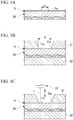
- Figs. 1A to 1D are explanatory views of the welding method according to the present embodiment, and show a cross section along the up-down direction.
- the first metal member 11 is superimposed on the upper surface of the second metal member 20 (preparation step).
- a hole 11a is formed in the first metal member 11 in advance.
- the shape of the hole 11a is preferably circular or substantially circular.
- the inner diameter (diameter) of the hole 11a is represented as a hole diameter D1.
- the hole diameter D1 is, for example, about 0.5 mm.
- the first metal member 11 and the second metal member 20 are fixed by jigs 31 and 32 (fixing step). More specifically, the first metal member 11 and the second metal member 20 are vertically sandwiched between the upper jig 31 and the lower jig 32.
- a jig hole 31a is formed in the upper jig 31.
- the inner diameter (diameter) of the jig hole 31a is represented as a jig hole diameter D2.
- the jig hole diameter D2 is, for example, 1 mm, and is larger than the hole diameter D1.
- the position of the upper jig 31 with respect to the first metal member 11 is determined such that the center of the jig hole 31a and the center of the hole 11a substantially match in plan view. Since the upper jig 31 and the lower jig 32 sandwich the first metal member 11 and the second metal member 20 with a predetermined pressure, the relative positions of the members are fixed.
- the laser light L is emitted downward from a laser apparatus 33 for welding and is applied near the hole 11a (irradiation step).
- the laser light L is applied to the first metal member 11 or the second metal member 20 through the jig hole 31a of the upper jig 31.
- the irradiation position of the laser light L moves so as to trace a predetermined trajectory T as shown in Fig. 2 .
- Fig. 2 is a view taken in the direction of arrow 11 in Fig. 1C .
- the dashed line in Fig. 2 indicates the trajectory T of the laser light L.
- the trajectory T in the present embodiment has a spiral shape substantially concentric with the hole 11a, starting at a first point X1 located radially outside the hole 11a and ending at a second point X2 located radially inside the hole 11a.
- the pitch of the spiral trajectory T is referred to as a pitch P.
- the distance between the central axis C of the hole 11a and the first point X1 is represented as an outer radius R1
- the distance between the central axis C and the second point X2 is represented as an inner radius R2.
- the trajectory T can be said to be substantially annular with an inner diameter of 2 ⁇ R2 and an outer diameter of 2 ⁇ R1.
- the hole diameter D1, the jig hole diameter D2, the outer radius R1, and the inner radius R2 are set so as to satisfy the following mathematical expression (1). 0 ⁇ R 2 ⁇ D 1 ⁇ 2 ⁇ R 1 ⁇ D 2 ⁇ 2
- the first metal member 11 and the second metal member 20 are partially melted.
- an interface between the non-melted portion 21 and the nugget portion (melted portion) 22 appears in the second metal member 20.
- An eutectic portion A is formed at the interface between the first metal member 11 and the second metal member 20.
- the non-melted portion 21 is a portion of the second metal member 20 that is not melted by the heat of the laser light L.
- the nugget portion 22 is a portion of the second metal member 20 that has been melted by the heat of the laser light L and then solidified again.
- the eutectic portion A is a portion where the first metal member 11 and the second metal member 20 are melted and mixed, and solidified in the eutectic state.
- the shapes of the non-melted portion 21, the nugget portion 22, and the eutectic portion A can be checked, for example, by cutting the portion or performing X-ray photography, after welding.
- Fig. 3 is an enlarged view around the nugget portion 22 in Fig. 1D .
- the interface between the nugget portion 22 and the non-melted portion 21 includes a protruding interface 21a that is convex upward.
- the protruding interface 21a is located at a radially central portion of the nugget portion 22. This is because the trajectory T of the laser light L is substantially annular in a top view, as described above. More specifically, since the laser light L is not applied near the central axis C in Fig. 2 , the portion closer to the central axis C of the second metal member 20 is not heated and is not melted. In addition, since the laser light L is applied from above, the lower part of the second metal member 20 does not receive transmitted heat and is not melted. Therefore, a protruding interface 21a as shown in Fig. 3 is formed.
- the bonding strength between the first metal member 11 and the second metal member 20 can be further increased.
- a part of the nugget portion 22 is exposed through the hole 11a. Further, the nugget portion 22 partially enters below the first metal member 11. In other words, the peripheral portion of the hole 11a in the first metal member 11 covers the nugget portion 22 from above. In the present embodiment, a portion of the first metal member 11 that covers the nugget portion 22 is called an overlap portion 11b.
- the reason why the overlap portion 11b is formed is that the melting point of the first metal member 11 is higher than the melting point of the second metal member 20. More specifically, as shown in Fig. 2 , when the first metal member 11 is irradiated with the laser light L, the temperature of the first metal member 11 rises, and the heat is transmitted to raise the temperature of the second metal member 20.
- the second metal member 20 having a lower melting point melts faster than the first metal member 11, the second metal member 20 located below the first metal member 11 remains liquid while the first metal member 11 remains solid.
- the overlap portion 11b covers the nugget portion 22.
- the area of the interface where the first metal member 11 and the second metal member 20 are welded increases, and the welding strength can be further increased.
- the inner diameter of the hole 11a after welding (hereinafter, referred to as a hole diameter D1' after welding) is larger than the hole diameter D1.
- a hole diameter D1' after welding is larger than the hole diameter D1.
- the eutectic portion A is formed over the inner peripheral surface of the hole 11a and the lower surface of the overlap portion 11b.
- the eutectic portion A is preferably thin because it is brittle and has low strength.
- the thickness of the eutectic portion A can be easily controlled by adjusting the dimensions P, R1, R2, D1, or the like.
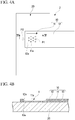
- the welding structure 1 of the present embodiment can be applied to a wiring board 2 with a metal piece as shown in Figs. 4A and 4B , for example.
- the wiring board 2 with a metal piece includes a flexible printed circuit (FPC) 10 and a metal piece (second metal member) 20.
- the flexible printed circuit 10 includes a wiring pattern (first metal member) 11, a base 13 and a coverlay 12 sandwiching the wiring pattern 11.
- the coverlay 12 and the base 13 are provided with rectangular openings 12a and 13a, respectively.
- the wiring pattern 11 is exposed through these openings 12a and 13a.
- a plurality of holes 11a are formed in the portion of the wiring pattern 11 that is exposed through the openings 12a and 13a. The exposed portion is bent downward and superimposed on the upper surface of the metal piece 20 through the opening 13a of the base 13.
- the wiring pattern 11 and the metal piece 20 are partially superimposed, and the wiring pattern 11 and the metal piece 20 are welded by using the bonding method shown in Figs. 1A to 1D , and these can be electrically connected. Further, by performing welding around each of the plurality of holes 11a, the bonding strength can be increased and the electric resistance can be reduced.
- the wiring board 2 with a metal piece as shown in Fig. 4A is manufactured by using the bonding method shown in Figs. 1A to 1D .
- the hole 11a is not formed in the first metal member (wiring pattern) 11 before welding.
- “Without holes” in Table 1 below indicates a sample in which the hole 11a is not formed before welding.
- “With holes” in Table 1 below indicates a sample in which holes 11a are formed before welding.
- the trajectory T of the laser light L is formed in a spiral shape as shown in Fig. 2 .
- the starting point of the trajectory T is a first point X1 located radially outside the hole 11a, and the ending point is a second point X2 located radially inside the hole 11a. That is, the trajectory T has a spiral shape from the outside to the inside of the hole 11a.
- the trajectory T of the laser light L has a pitch P of 0.04 mm, an outer radius R1 of 0.375 mm, and an inner radius R2 of 0.155 mm.
- the laser apparatus 33 uses a fiber laser having a maximum output of 300 W.
- a galvano scanner is used for movement to trace the trajectory T.
- the laser output in Table 1 shows the ratio to the maximum output, and is set to 70% to 80% in the present example.
- the scanning speed when the laser light L traces the trajectory T is 600 mm/s.
- the jig hole diameter D2 is 1 mm.
- the first metal member 11 is a copper foil having a thickness of 0.035 mm.
- a total of ten holes 11a arranged as shown in Fig. 4A are formed in the first metal member 11.
- Each hole diameter D1 is 0.5 mm.
- the second metal member 20 is an aluminum plate (A1050) having a thickness of 1 mm. Note that the conditions for the sample "without holes” are the same as the conditions for the sample "with holes", except that the hole 11a is not formed.
- the hole diameter D1' after welding (see Fig. 3 ) of the sample with holes is 0.85 to 0.9 mm.
- Resistance value shown in Table 1 is a result of measuring the electric resistance between points P1 and P2 shown in Fig. 4A for each sample.
- the interval between the points P1 and P2 is 10 mm.
- the sample without holes has an average resistance value of 0.35 m ⁇ , and the sample with holes has an average resistance value of 0.23 m ⁇ .
- the electric resistance can be reduced by about 34% by forming the hole 11a in advance.
- “Bonding strength” shown in Table 1 is a result of measuring the bonding strength of each sample using a tensile tester as shown in Fig. 5 . More specifically, the flexible printed circuit 10 is clamped by the first clamp K1, and the metal piece 20 is clamped by the second clamp K2. Then, the maximum value of the tensile force when the first clamp K1 and the second clamp K2 are separated at a speed of 10 mm/min is recorded as the bonding strength.
- the sample without holes has an average bonding strength of 2.76 kgf, and the sample with holes has an average bonding strength of 3.47 kgf.
- the bonding strength can be improved by about 26%. This is because the welding structure shown in Fig. 3 is obtained by forming the hole 11a in advance, and separation (peeling) is less likely to occur between the first metal member 11 and the second metal member 20 or between the nugget portion 22 and the non-melted portion 21.
- the welding method of the present embodiment includes the preparation step of superimposing the first metal member 11 having the hole 11a formed thereon on the upper surface of the second metal member 20, and the irradiation step of applying laser light L near the hole 11a from above to weld the first metal member 11 and the second metal member 20. Then, in a top view, the trajectory T of the laser light L in the irradiation step is annular from the first point X1 located outside the hole 11a to the second point X2 located inside the hole 11a (across the hole 11a). Thereby, the welding structure 1 as shown in Fig. 3 is obtained.
- the peripheral portion of the hole 11a covers the nugget portion 22 of the second metal member 20.
- the area of the interface where the first metal member 11 and the second metal member 20 are bonded increases, and the bonding strength can be improved. Further, as shown in the example, the electric resistance between the first metal member 11 and the second metal member 20 can be reduced.
- the interface between the nugget portion 22 and the non-melted portion 21 in the second metal member 20 includes a protruding interface 21a that protrudes upward.
- the occurrence of separation (peeling) between the non-melted portion 21 and the nugget portion 22 is suppressed, and the bonding strength can be more reliably increased.
- the second metal member 20 melts faster than the first metal member 11, so that the overlap portion 11b of the first metal member 11 is easily formed.
- the thickness of the eutectic portion A can be easily controlled by adjusting the welding parameters P, R1, R2, D1, or the like, because the trajectory T of the laser light L is spiral in a top view.
- the bonding strength between the wiring pattern 11 and the metal piece 20 is increased, and the electric resistance between the wiring pattern 11 and the metal piece 20 can be reduced.
- the welding method and the welding structure 1 of the above embodiment may be used for applications other than the wiring board 2 with a metal piece.
- trajectory T of the laser light L may be directed from the radial inside (the second point X2) of the hole 11a to the radial outside (the first point X1).
- trajectory T may be substantially annular as a whole, for example, by making the trajectory radial about the central axis C.
Landscapes
- Engineering & Computer Science (AREA)
- Physics & Mathematics (AREA)
- Optics & Photonics (AREA)
- Plasma & Fusion (AREA)
- Mechanical Engineering (AREA)
- Manufacturing & Machinery (AREA)
- Microelectronics & Electronic Packaging (AREA)
- Laser Beam Processing (AREA)
- Connections Effected By Soldering, Adhesion, Or Permanent Deformation (AREA)
- Coupling Device And Connection With Printed Circuit (AREA)
Abstract
Description
- The present invention relates to a welding structure, a wiring board with a metal piece, and a welding method.
- Priority is claimed on Japanese Patent Application No.
2017-253541 filed on December 28, 2017 - In the related art, as shown in
PTL 1, a welding method in which a first metal member and a second metal member are superimposed and an interface between the two members is irradiated with laser light has been known. After welding, the first metal member and the second metal member are fixed and electrically connected. - [Patent Document 1]
Japanese Unexamined Patent Application, First publication No.H 10-334956 - In this type of welding method, bonding strength and electric resistance need to be improved.
- The present invention has been made in view of such circumstances, and an object is to improve bonding strength and reduce electric resistance in a welding structure.
- In order to solve the above-described problems, a welding structure according to a first aspect of the present invention includes a first metal member and a second metal member that are superimposed and welded together, in which the first metal member has a hole, the second metal member has a nugget portion that is solidified again after being melted by heat, a peripheral portion of the hole in the first metal member covers the nugget portion, and a part of the nugget portion is exposed through the hole.
- Here, in a cross-sectional view along an up-down direction in which the first metal member and the second metal member are superimposed, an interface between the nugget portion and the non-melted portion in the second metal member may include a protruding interface that protrudes toward the first metal member in the up-down direction.
- A wiring board with a metal piece according to the second aspect of the present invention includes a flexible printed circuit having a wiring pattern, and a base and a coverlay sandwiching the wiring pattern; and a metal piece welded to the wiring pattern, in which the wiring pattern has a hole, the metal piece has a nugget portion that is solidified again after being melted by heat, a peripheral portion of the hole in the wiring pattern covers the nugget portion, and a part of the nugget portion is exposed through the hole.
- The welding method according to a third aspect of the present invention includes a preparation step of superimposing a first metal member having copper as a main component and a hole formed thereon on an upper surface of a second metal member having aluminum as a main component; and an irradiation step of applying laser light near the hole from above to weld the first metal member and the second metal member, in which a trajectory of the laser light in the irradiation step is spiral across the hole, in a top view.
- A welding method according to a fourth aspect of the present invention includes a preparation step of superimposing a first metal member having a hole on an upper surface of a second metal member; a fixing step of fixing the first metal member and the second metal member with a jig; and an irradiation step of applying laser light near the hole from above through a jig hole formed in the jig to weld the first metal member and the second metal member, in which in a top view, a trajectory of the laser light in the irradiation step is annular from a first point located outside the hole to a second point located inside the hole, and 0 < R2 < D1 ÷ 2 < R1 < D2 ÷ 2 is satisfied when a diameter of the hole is represented by D1, a diameter of the jig hole is represented by D2, a distance between a central axis of the hole and the first point is represented by R1, and a distance between the central axis and the second point is represented by R2.
- In the welding method according to the fourth aspect, a main component of the first metal member may be copper, a main component of the second metal member may be aluminum, and the trajectory may be spiral in a top view.
- According to the aspect of the present invention, in a welding structure, bonding strength can be improved and electric resistance can be reduced.
-
-
Fig. 1A is a schematic diagram showing a welding method according to the present embodiment. -
Fig. 1B is a diagram showing a step followingFig. 1A . -
Fig. 1C is a diagram showing a step followingFig. 1B . -
Fig. 1D is a diagram showing a step followingFig. 1C . -
Fig. 2 is a view taken in the direction of arrow II inFig. 1C . -
Fig. 3 is a sectional view of the welding structure according to the present embodiment. -
Fig. 4A is a top view of the wiring board with a metal piece according to the present embodiment. -
Fig. 4B is a sectional view taken along line IV-IV inFig. 4A . -
Fig. 5 is a diagram showing a method of testing bonding strength. - Hereinafter, a welding method, a welding structure, and a wiring board with a metal piece according to the present embodiment will be described with reference to the drawings. Note that the present invention is not limited to the following embodiments.
- In the present embodiment, a description will be given of a welding method or the like for welding the
first metal member 11 of a thin film shape as shown inFig. 1A to thesecond metal member 20. Thefirst metal member 11 is superimposed on the surface (upper surface) of thesecond metal member 20. Hereinafter, the direction in which thefirst metal member 11 and thesecond metal member 20 are superimposed is referred to as an up-down direction. Further, along the up-down direction, thefirst metal member 11 side is referred to as an upper side, and thesecond metal member 20 side is referred to as a lower side. - A straight line that passes through the center of a
hole 11a described later in thefirst metal member 11 and extends in the up-down direction is referred to as a central axis C (seeFigs. 2 and3 ). A direction that intersects the central axis C in plan view as viewed in the up-down direction is referred to as a radial direction. - The
first metal member 11 is formed in a thin film shape. The shape of thesecond metal member 20 is not particularly limited, but may be a film shape, a plate shape, a block shape, or the like. The materials of thefirst metal member 11 and thesecond metal member 20 are different from each other. The melting point of thefirst metal member 11 is preferably higher than the melting point of thesecond metal member 20. Thefirst metal member 11 is formed of, for example, a metal (copper alloy) containing copper as a main component. Thesecond metal member 20 is formed of, for example, a metal (aluminum alloy) containing aluminum as a main component. -
Figs. 1A to 1D are explanatory views of the welding method according to the present embodiment, and show a cross section along the up-down direction. When welding thefirst metal member 11 and thesecond metal member 20, first, as shown inFig. 1A , thefirst metal member 11 is superimposed on the upper surface of the second metal member 20 (preparation step). At this time, ahole 11a is formed in thefirst metal member 11 in advance. The shape of thehole 11a is preferably circular or substantially circular. In the present embodiment, the inner diameter (diameter) of thehole 11a is represented as a hole diameter D1. The hole diameter D1 is, for example, about 0.5 mm. - Next, as shown in
Fig. 1B , thefirst metal member 11 and thesecond metal member 20 are fixed byjigs 31 and 32 (fixing step). More specifically, thefirst metal member 11 and thesecond metal member 20 are vertically sandwiched between theupper jig 31 and thelower jig 32. Ajig hole 31a is formed in theupper jig 31. In the present embodiment, the inner diameter (diameter) of thejig hole 31a is represented as a jig hole diameter D2. The jig hole diameter D2 is, for example, 1 mm, and is larger than the hole diameter D1. The position of theupper jig 31 with respect to thefirst metal member 11 is determined such that the center of thejig hole 31a and the center of thehole 11a substantially match in plan view. Since theupper jig 31 and thelower jig 32 sandwich thefirst metal member 11 and thesecond metal member 20 with a predetermined pressure, the relative positions of the members are fixed. - Next, as shown in
Fig. 1C , the laser light L is emitted downward from alaser apparatus 33 for welding and is applied near thehole 11a (irradiation step). The laser light L is applied to thefirst metal member 11 or thesecond metal member 20 through thejig hole 31a of theupper jig 31. At this time, the irradiation position of the laser light L moves so as to trace a predetermined trajectory T as shown inFig. 2 . -
Fig. 2 is a view taken in the direction ofarrow 11 inFig. 1C . The dashed line inFig. 2 indicates the trajectory T of the laser light L. In a top view, the trajectory T in the present embodiment has a spiral shape substantially concentric with thehole 11a, starting at a first point X1 located radially outside thehole 11a and ending at a second point X2 located radially inside thehole 11a. Hereinafter, the pitch of the spiral trajectory T is referred to as a pitch P. Further, in a top view, the distance between the central axis C of thehole 11a and the first point X1 is represented as an outer radius R1, and the distance between the central axis C and the second point X2 is represented as an inner radius R2. The trajectory T can be said to be substantially annular with an inner diameter of 2 × R2 and an outer diameter of 2 × R1. The hole diameter D1, the jig hole diameter D2, the outer radius R1, and the inner radius R2 are set so as to satisfy the following mathematical expression (1).
- By applying the laser light L, the
first metal member 11 and thesecond metal member 20 are partially melted. Thereby, as shown inFig. 1D , an interface between thenon-melted portion 21 and the nugget portion (melted portion) 22 appears in thesecond metal member 20. An eutectic portion A is formed at the interface between thefirst metal member 11 and thesecond metal member 20. Here, thenon-melted portion 21 is a portion of thesecond metal member 20 that is not melted by the heat of the laser light L. The nugget portion 22 is a portion of thesecond metal member 20 that has been melted by the heat of the laser light L and then solidified again. The eutectic portion A is a portion where thefirst metal member 11 and thesecond metal member 20 are melted and mixed, and solidified in the eutectic state. The shapes of thenon-melted portion 21, the nugget portion 22, and the eutectic portion A can be checked, for example, by cutting the portion or performing X-ray photography, after welding. - Next, the
welding structure 1 obtained by the above welding method will be described with reference toFig. 3. Fig. 3 is an enlarged view around the nugget portion 22 inFig. 1D . As shown inFig. 3 , the interface between the nugget portion 22 and thenon-melted portion 21 includes a protrudinginterface 21a that is convex upward. The protrudinginterface 21a is located at a radially central portion of the nugget portion 22. This is because the trajectory T of the laser light L is substantially annular in a top view, as described above. More specifically, since the laser light L is not applied near the central axis C inFig. 2 , the portion closer to the central axis C of thesecond metal member 20 is not heated and is not melted. In addition, since the laser light L is applied from above, the lower part of thesecond metal member 20 does not receive transmitted heat and is not melted. Therefore, a protrudinginterface 21a as shown inFig. 3 is formed. - By forming such a protruding
interface 21a, separation (peeling) is less likely to occur at the interface between thenon-melted portion 21 and the nugget portion 22, and the bonding strength can be increased. Further, the nugget portion 22 has a shape that partially enters the inside of thehole 11a of thefirst metal member 11 in the radial direction and is fitted into thehole 11a. Thereby, the bonding strength between thefirst metal member 11 and thesecond metal member 20 can be further increased. - A part of the nugget portion 22 is exposed through the
hole 11a. Further, the nugget portion 22 partially enters below thefirst metal member 11. In other words, the peripheral portion of thehole 11a in thefirst metal member 11 covers the nugget portion 22 from above. In the present embodiment, a portion of thefirst metal member 11 that covers the nugget portion 22 is called anoverlap portion 11b. The reason why theoverlap portion 11b is formed is that the melting point of thefirst metal member 11 is higher than the melting point of thesecond metal member 20. More specifically, as shown inFig. 2 , when thefirst metal member 11 is irradiated with the laser light L, the temperature of thefirst metal member 11 rises, and the heat is transmitted to raise the temperature of thesecond metal member 20. Since thesecond metal member 20 having a lower melting point melts faster than thefirst metal member 11, thesecond metal member 20 located below thefirst metal member 11 remains liquid while thefirst metal member 11 remains solid. By solidifying the liquidsecond metal member 20, theoverlap portion 11b covers the nugget portion 22. - By forming the
overlap portion 11b in this manner, the area of the interface where thefirst metal member 11 and thesecond metal member 20 are welded increases, and the welding strength can be further increased. - In addition, the inner diameter of the
hole 11a after welding (hereinafter, referred to as a hole diameter D1' after welding) is larger than the hole diameter D1. This is because the portion of thefirst metal member 11 near thehole 11a is melted and mixed with thesecond metal member 20 to form the eutectic portion A. The eutectic portion A is formed over the inner peripheral surface of thehole 11a and the lower surface of theoverlap portion 11b. The eutectic portion A is preferably thin because it is brittle and has low strength. In the present embodiment, the thickness of the eutectic portion A can be easily controlled by adjusting the dimensions P, R1, R2, D1, or the like. - The
welding structure 1 of the present embodiment can be applied to awiring board 2 with a metal piece as shown inFigs. 4A and 4B , for example. Thewiring board 2 with a metal piece includes a flexible printed circuit (FPC) 10 and a metal piece (second metal member) 20. - As shown in
Fig. 4B , the flexible printedcircuit 10 includes a wiring pattern (first metal member) 11, abase 13 and acoverlay 12 sandwiching thewiring pattern 11. In the example ofFigs. 4A and 4B , thecoverlay 12 and the base 13 are provided withrectangular openings wiring pattern 11 is exposed through theseopenings holes 11a are formed in the portion of thewiring pattern 11 that is exposed through theopenings metal piece 20 through theopening 13a of thebase 13. - As described above, the
wiring pattern 11 and themetal piece 20 are partially superimposed, and thewiring pattern 11 and themetal piece 20 are welded by using the bonding method shown inFigs. 1A to 1D , and these can be electrically connected. Further, by performing welding around each of the plurality ofholes 11a, the bonding strength can be increased and the electric resistance can be reduced. - Next, the effect of the presence or absence of the
hole 11a on the bonding strength and the electric resistance will be described using an example. - In the present example, the
wiring board 2 with a metal piece as shown inFig. 4A is manufactured by using the bonding method shown inFigs. 1A to 1D . However, in some samples, thehole 11a is not formed in the first metal member (wiring pattern) 11 before welding. "Without holes" in Table 1 below indicates a sample in which thehole 11a is not formed before welding. "With holes" in Table 1 below indicates a sample in which holes 11a are formed before welding.[Table 1] Resistance Value (mΩ) Bonding Strength (kgf) Laser Output Without holes With holes Without holes With holes 80% 0.31 0.21 3.13 3.62 80% 0.42 0.23 2.28 3.36 70% 0.33 0.26 2.86 3.42 Average 0.35 0.23 2.76 3.47 - In the present example, the trajectory T of the laser light L is formed in a spiral shape as shown in
Fig. 2 . The starting point of the trajectory T is a first point X1 located radially outside thehole 11a, and the ending point is a second point X2 located radially inside thehole 11a. That is, the trajectory T has a spiral shape from the outside to the inside of thehole 11a. The trajectory T of the laser light L has a pitch P of 0.04 mm, an outer radius R1 of 0.375 mm, and an inner radius R2 of 0.155 mm. Thelaser apparatus 33 uses a fiber laser having a maximum output of 300 W. A galvano scanner is used for movement to trace the trajectory T. - The laser output in Table 1 shows the ratio to the maximum output, and is set to 70% to 80% in the present example. The scanning speed when the laser light L traces the trajectory T is 600 mm/s. The jig hole diameter D2 is 1 mm. The
first metal member 11 is a copper foil having a thickness of 0.035 mm. In the "with holes" sample, a total of tenholes 11a arranged as shown inFig. 4A are formed in thefirst metal member 11. Each hole diameter D1 is 0.5 mm. Thesecond metal member 20 is an aluminum plate (A1050) having a thickness of 1 mm. Note that the conditions for the sample "without holes" are the same as the conditions for the sample "with holes", except that thehole 11a is not formed. - Under the above conditions, the hole diameter D1' after welding (see
Fig. 3 ) of the sample with holes is 0.85 to 0.9 mm. - "Resistance value" shown in Table 1 is a result of measuring the electric resistance between points P1 and P2 shown in
Fig. 4A for each sample. The interval between the points P1 and P2 is 10 mm. - As shown in Table 1, the sample without holes has an average resistance value of 0.35 mΩ, and the sample with holes has an average resistance value of 0.23 mΩ. Thus, the electric resistance can be reduced by about 34% by forming the
hole 11a in advance. - "Bonding strength" shown in Table 1 is a result of measuring the bonding strength of each sample using a tensile tester as shown in
Fig. 5 . More specifically, the flexible printedcircuit 10 is clamped by the first clamp K1, and themetal piece 20 is clamped by the second clamp K2. Then, the maximum value of the tensile force when the first clamp K1 and the second clamp K2 are separated at a speed of 10 mm/min is recorded as the bonding strength. - As shown in Table 1, the sample without holes has an average bonding strength of 2.76 kgf, and the sample with holes has an average bonding strength of 3.47 kgf. Thus, by forming the
hole 11a in advance, the bonding strength can be improved by about 26%. This is because the welding structure shown inFig. 3 is obtained by forming thehole 11a in advance, and separation (peeling) is less likely to occur between thefirst metal member 11 and thesecond metal member 20 or between the nugget portion 22 and thenon-melted portion 21. - As described above, the welding method of the present embodiment includes the preparation step of superimposing the
first metal member 11 having thehole 11a formed thereon on the upper surface of thesecond metal member 20, and the irradiation step of applying laser light L near thehole 11a from above to weld thefirst metal member 11 and thesecond metal member 20. Then, in a top view, the trajectory T of the laser light L in the irradiation step is annular from the first point X1 located outside thehole 11a to the second point X2 located inside thehole 11a (across thehole 11a). Thereby, thewelding structure 1 as shown inFig. 3 is obtained. - In the
welding structure 1, the peripheral portion of thehole 11a covers the nugget portion 22 of thesecond metal member 20. Thereby, the area of the interface where thefirst metal member 11 and thesecond metal member 20 are bonded increases, and the bonding strength can be improved. Further, as shown in the example, the electric resistance between thefirst metal member 11 and thesecond metal member 20 can be reduced. - Further, as shown in
Fig. 3 , in a cross-sectional view along the up-down direction, the interface between the nugget portion 22 and thenon-melted portion 21 in thesecond metal member 20 includes a protrudinginterface 21a that protrudes upward. Thereby, the occurrence of separation (peeling) between thenon-melted portion 21 and the nugget portion 22 is suppressed, and the bonding strength can be more reliably increased. - Further, since the melting point of the
first metal member 11 is higher than the melting point of thesecond metal member 20, thesecond metal member 20 melts faster than thefirst metal member 11, so that theoverlap portion 11b of thefirst metal member 11 is easily formed. - The thickness of the eutectic portion A can be easily controlled by adjusting the welding parameters P, R1, R2, D1, or the like, because the trajectory T of the laser light L is spiral in a top view.
- Further, by applying the welding method or the
welding structure 1 as described above to thewiring board 2 with a metal piece, the bonding strength between thewiring pattern 11 and themetal piece 20 is increased, and the electric resistance between thewiring pattern 11 and themetal piece 20 can be reduced. - It should be noted that the technical scope of the present invention is not limited to the above-described embodiments, and various modifications can be made without departing from the spirit of the present invention.
- For example, the welding method and the
welding structure 1 of the above embodiment may be used for applications other than thewiring board 2 with a metal piece. - Further, the trajectory T of the laser light L may be directed from the radial inside (the second point X2) of the
hole 11a to the radial outside (the first point X1). - Further, the trajectory T may be substantially annular as a whole, for example, by making the trajectory radial about the central axis C.
- In addition, without departing from the spirit of the present invention, it is possible to appropriately replace the constituent elements in the above-described embodiment with well-known constituent elements, and the above-described embodiment and modification examples may be appropriately combined.
-
- 1 Welding structure
- 2 Wiring board with metal piece
- 10 Flexible printed circuit
- 11 First metal member (wiring pattern)
- 11a Hole
- 12 Coverlay
- 13 Base
- 20 Second metal member (metal piece)
- 22 Nugget portion
- 21a Protruding interface
Claims (6)
- A welding structure comprising:a first metal member and a second metal member that are superimposed and welded together,wherein the first metal member has a hole,wherein the second metal member has a nugget portion that is solidified again after being melted by heat,wherein a peripheral portion of the hole in the first metal member covers the nugget portion, andwherein a part of the nugget portion is exposed through the hole.
- The welding structure according to claim 1,
wherein in a cross-sectional view along an up-down direction in which the first metal member and the second metal member are superimposed, an interface between the nugget portion and a non-melted portion in the second metal member includes a protruding interface that protrudes toward the first metal member in the up-down direction. - A wiring board with a metal piece comprising:a flexible printed circuit having a wiring pattern, and a base and a coverlay sandwiching the wiring pattern; anda metal piece welded to the wiring pattern,wherein the wiring pattern has a hole,wherein the metal piece has a nugget portion that is solidified again after being melted by heat,wherein a peripheral portion of the hole in the wiring pattern covers the nugget portion, andwherein a part of the nugget portion is exposed through the hole.
- A welding method comprising:a preparation step of superimposing a first metal member having a main component of copper and having a hole on an upper surface of a second metal member having a main component of aluminum; andan irradiation step of applying laser light near the hole from above to weld the first metal member and the second metal member,wherein a trajectory of the laser light in the irradiation step is spiral across the hole, in a top view.
- A welding method comprising:a preparation step of superimposing a first metal member having a hole on an upper surface of a second metal member;a fixing step of fixing the first metal member and the second metal member with a jig; andan irradiation step of applying laser light near the hole from above through a jig hole formed in the jig to weld the first metal member and the second metal member, whereinin a top view, a trajectory of the laser light in the irradiation step is annular from a first point located outside the hole to a second point located inside the hole, and0 < R2 < D1 ÷ 2 < R1 < D2 ÷ 2 is satisfied when a diameter of the hole is represented by D1, a diameter of the jig hole is represented by D2, a distance between a central axis of the hole and the first point is represented by R1, and a distance between the central axis and the second point is represented by R2.
- The welding method according to claim 5,
wherein a main component of the first metal member is copper, and a main component of the second metal member is aluminum, and
wherein the trajectory is spiral in a top view.
Applications Claiming Priority (2)
| Application Number | Priority Date | Filing Date | Title |
|---|---|---|---|
| JP2017253541 | 2017-12-28 | ||
| PCT/JP2018/048031 WO2019131828A1 (en) | 2017-12-28 | 2018-12-27 | Welding structure, wiring board equipped with metal piece, and welding method |
Publications (3)
| Publication Number | Publication Date |
|---|---|
| EP3733339A1 true EP3733339A1 (en) | 2020-11-04 |
| EP3733339A4 EP3733339A4 (en) | 2021-11-17 |
| EP3733339B1 EP3733339B1 (en) | 2024-02-07 |
Family
ID=67063789
Family Applications (1)
| Application Number | Title | Priority Date | Filing Date |
|---|---|---|---|
| EP18895465.5A Active EP3733339B1 (en) | 2017-12-28 | 2018-12-27 | Welding structure, wiring board with metal piece |
Country Status (5)
| Country | Link |
|---|---|
| US (1) | US11597038B2 (en) |
| EP (1) | EP3733339B1 (en) |
| JP (1) | JP6896889B2 (en) |
| CN (2) | CN113618237B (en) |
| WO (1) | WO2019131828A1 (en) |
Families Citing this family (7)
| Publication number | Priority date | Publication date | Assignee | Title |
|---|---|---|---|---|
| WO2021111966A1 (en) * | 2019-12-05 | 2021-06-10 | 株式会社フジクラ | Wiring board having metal piece |
| DE102021120217B3 (en) * | 2021-08-04 | 2022-09-29 | Lisa Dräxlmaier GmbH | Device and method for contacting a conductor |
| CN114346601B (en) * | 2021-12-28 | 2023-01-31 | 富联裕展科技(深圳)有限公司 | Composite material structure and processing method thereof |
| US20240408699A1 (en) * | 2022-05-31 | 2024-12-12 | Lg Energy Solution, Ltd. | Laser welding apparatus and welding method using the same |
| JP2024013085A (en) * | 2022-07-19 | 2024-01-31 | 矢崎総業株式会社 | Metal plate joining method, busbar module manufacturing method, and battery module manufacturing method |
| EP4366085A4 (en) * | 2022-09-23 | 2024-11-13 | Samsung Electronics Co., Ltd. | Electronic device comprising antenna structure connected to housing |
| CN118616910B (en) * | 2024-08-09 | 2024-10-25 | 北京金橙子科技股份有限公司 | Cross filling method for annular patterns and storage medium |
Family Cites Families (21)
| Publication number | Priority date | Publication date | Assignee | Title |
|---|---|---|---|---|
| JPS6057430B2 (en) * | 1980-11-29 | 1985-12-14 | 松下電工株式会社 | Welding method using laser beam |
| US5306891A (en) | 1992-04-02 | 1994-04-26 | Motorola, Inc. | Laser welding process for attaching metal to ceramic substrate |
| JPH08332582A (en) * | 1995-06-05 | 1996-12-17 | Toshiba Corp | Laser welding method |
| JPH10334956A (en) | 1997-05-28 | 1998-12-18 | Harness Sogo Gijutsu Kenkyusho:Kk | Laser welding structure |
| JP3343066B2 (en) * | 1997-11-04 | 2002-11-11 | 株式会社オートネットワーク技術研究所 | Laser welding structure of bus bar |
| JP2005123419A (en) * | 2003-10-17 | 2005-05-12 | Tohoku Pioneer Corp | Wiring board, wiring pattern forming method, organic EL panel |
| JP2005347143A (en) | 2004-06-04 | 2005-12-15 | Fujikura Ltd | connector |
| JP2007265962A (en) | 2006-02-28 | 2007-10-11 | Hitachi Ltd | Laser welding method, control unit manufacturing method, and vehicle control unit |
| JP5118862B2 (en) * | 2007-03-05 | 2013-01-16 | トヨタ自動車株式会社 | Laser bonding method |
| JP5248344B2 (en) | 2009-01-20 | 2013-07-31 | 本田技研工業株式会社 | Laser welding method |
| EP2684637B1 (en) | 2011-05-30 | 2017-09-06 | Panasonic Intellectual Property Management Co., Ltd. | Laser welding component and method for manufacturing same |
| JP5932323B2 (en) * | 2011-12-19 | 2016-06-08 | 株式会社東芝 | Secondary battery and method for manufacturing secondary battery |
| CN102896398A (en) | 2012-10-10 | 2013-01-30 | 上海交通大学 | Aluminum alloy arc spot welding method based on CMT (Cold Metal Transmission Welding) and welding system |
| WO2014123022A1 (en) | 2013-02-05 | 2014-08-14 | 株式会社日立製作所 | Laser joining apparatus and laser joining method |
| WO2015016287A1 (en) * | 2013-07-31 | 2015-02-05 | 新日鐵住金株式会社 | Arc spot weld joint and method for producing same |
| EP3093096B1 (en) | 2014-01-10 | 2022-12-07 | Panasonic Intellectual Property Management Co., Ltd. | Laser welding method and laser welding device |
| EP3112077B1 (en) * | 2014-02-25 | 2021-03-31 | Panasonic Intellectual Property Management Co., Ltd. | Laser welding method |
| CN105855706B (en) | 2015-02-09 | 2018-02-13 | 司浦爱激光技术英国有限公司 | laser weld |
| GB201502149D0 (en) | 2015-02-09 | 2015-03-25 | Spi Lasers Uk Ltd | Apparatus and method for laser welding |
| JP6149887B2 (en) * | 2015-04-03 | 2017-06-21 | トヨタ自動車株式会社 | Welding method |
| US10118249B2 (en) | 2015-10-15 | 2018-11-06 | GM Global Technology Operations LLC | Laser beam welding with a spiral weld path having a first order of continuity |
-
2018
- 2018-12-27 WO PCT/JP2018/048031 patent/WO2019131828A1/en not_active Ceased
- 2018-12-27 CN CN202110880212.3A patent/CN113618237B/en active Active
- 2018-12-27 JP JP2019562141A patent/JP6896889B2/en active Active
- 2018-12-27 US US16/650,726 patent/US11597038B2/en active Active
- 2018-12-27 EP EP18895465.5A patent/EP3733339B1/en active Active
- 2018-12-27 CN CN201880061937.6A patent/CN111163896B/en active Active
Also Published As
| Publication number | Publication date |
|---|---|
| EP3733339A4 (en) | 2021-11-17 |
| WO2019131828A1 (en) | 2019-07-04 |
| CN111163896B (en) | 2022-10-04 |
| US20200306882A1 (en) | 2020-10-01 |
| US11597038B2 (en) | 2023-03-07 |
| CN113618237B (en) | 2023-09-22 |
| CN113618237A (en) | 2021-11-09 |
| JP6896889B2 (en) | 2021-06-30 |
| CN111163896A (en) | 2020-05-15 |
| JPWO2019131828A1 (en) | 2020-11-19 |
| EP3733339B1 (en) | 2024-02-07 |
Similar Documents
| Publication | Publication Date | Title |
|---|---|---|
| EP3733339B1 (en) | Welding structure, wiring board with metal piece | |
| JP4554873B2 (en) | Wiring board, electronic device, electronic component mounting method and manufacturing method | |
| EP3132884A1 (en) | Joined body of dissimilar metals | |
| JP2018192515A (en) | Metal thin plate / base material joint structure and metal thin plate / base material welding method | |
| JP2014099537A (en) | Flexible printed circuit board bonding method | |
| EP2554967A1 (en) | Pressure-sensitive device and method of welding joint of pressure-sensitive device | |
| JP7110907B2 (en) | Lap welding method for dissimilar metal members | |
| CN101663717B (en) | Process for manufacturing lead terminal for capacitor | |
| EP2684637A1 (en) | Laser welding component and method for manufacturing same | |
| US7770290B2 (en) | Electrical connection method for plural coaxial wires | |
| JP2012004281A (en) | Laser welding method, electronic component connection structure, and laser welding inspection method | |
| WO2015111509A1 (en) | Terminal fitting-equipped electrical wire and method for manufacturing same | |
| JP2020097039A (en) | Lap-welding method of dissimilar metal member | |
| WO2015170539A1 (en) | Resin multilayer substrate and method for producing same | |
| US20110286193A1 (en) | Assembly of at least two electric boards | |
| US8373091B2 (en) | Method of manufacturing a contact | |
| US9844146B2 (en) | Electrical circuitry assembly and method for manufacturing the same | |
| DE102021203077A1 (en) | Electronic component and method and device for manufacturing an electronic component | |
| EP2285197B1 (en) | Method for connecting an electronic component with a circuit board | |
| WO2021111966A1 (en) | Wiring board having metal piece | |
| US20190269020A1 (en) | System and method for connecting flat flexible cable to printed circuit board | |
| JP7128381B2 (en) | Electronic component, lead connection structure and lead connection method | |
| WO2019172025A1 (en) | Joining structure and joining method | |
| JP2007188979A (en) | Inter-board connection structure and printed wiring board | |
| JP3321660B2 (en) | Board structure with terminal strip |
Legal Events
| Date | Code | Title | Description |
|---|---|---|---|
| STAA | Information on the status of an ep patent application or granted ep patent |
Free format text: STATUS: THE INTERNATIONAL PUBLICATION HAS BEEN MADE |
|
| PUAI | Public reference made under article 153(3) epc to a published international application that has entered the european phase |
Free format text: ORIGINAL CODE: 0009012 |
|
| STAA | Information on the status of an ep patent application or granted ep patent |
Free format text: STATUS: REQUEST FOR EXAMINATION WAS MADE |
|
| 17P | Request for examination filed |
Effective date: 20200323 |
|
| AK | Designated contracting states |
Kind code of ref document: A1 Designated state(s): AL AT BE BG CH CY CZ DE DK EE ES FI FR GB GR HR HU IE IS IT LI LT LU LV MC MK MT NL NO PL PT RO RS SE SI SK SM TR |
|
| AX | Request for extension of the european patent |
Extension state: BA ME |
|
| DAV | Request for validation of the european patent (deleted) | ||
| DAX | Request for extension of the european patent (deleted) | ||
| A4 | Supplementary search report drawn up and despatched |
Effective date: 20211014 |
|
| RIC1 | Information provided on ipc code assigned before grant |
Ipc: B23K 103/12 20060101ALN20211008BHEP Ipc: B23K 103/10 20060101ALN20211008BHEP Ipc: B23K 101/42 20060101ALN20211008BHEP Ipc: H05K 3/32 20060101ALI20211008BHEP Ipc: H05K 1/11 20060101ALI20211008BHEP Ipc: H01R 43/02 20060101ALI20211008BHEP Ipc: H01R 12/62 20110101ALI20211008BHEP Ipc: H01R 4/02 20060101ALI20211008BHEP Ipc: B23K 26/323 20140101ALI20211008BHEP Ipc: B23K 26/244 20140101ALI20211008BHEP Ipc: B23K 26/24 20140101AFI20211008BHEP |
|
| STAA | Information on the status of an ep patent application or granted ep patent |
Free format text: STATUS: EXAMINATION IS IN PROGRESS |
|
| 17Q | First examination report despatched |
Effective date: 20220920 |
|
| REG | Reference to a national code |
Ref country code: DE Ref legal event code: R079 Free format text: PREVIOUS MAIN CLASS: B23K0026210000 Ipc: B23K0026240000 Ref country code: DE Ref legal event code: R079 Ref document number: 602018065077 Country of ref document: DE Free format text: PREVIOUS MAIN CLASS: B23K0026210000 Ipc: B23K0026240000 |
|
| GRAP | Despatch of communication of intention to grant a patent |
Free format text: ORIGINAL CODE: EPIDOSNIGR1 |
|
| STAA | Information on the status of an ep patent application or granted ep patent |
Free format text: STATUS: GRANT OF PATENT IS INTENDED |
|
| RIC1 | Information provided on ipc code assigned before grant |
Ipc: B23K 103/12 20060101ALN20230713BHEP Ipc: B23K 103/10 20060101ALN20230713BHEP Ipc: B23K 101/42 20060101ALN20230713BHEP Ipc: H05K 3/32 20060101ALI20230713BHEP Ipc: H05K 1/11 20060101ALI20230713BHEP Ipc: H01R 43/02 20060101ALI20230713BHEP Ipc: H01R 12/62 20110101ALI20230713BHEP Ipc: H01R 4/02 20060101ALI20230713BHEP Ipc: B23K 26/323 20140101ALI20230713BHEP Ipc: B23K 26/244 20140101ALI20230713BHEP Ipc: B23K 26/24 20140101AFI20230713BHEP |
|
| RIC1 | Information provided on ipc code assigned before grant |
Ipc: B23K 103/12 20060101ALN20230718BHEP Ipc: B23K 103/10 20060101ALN20230718BHEP Ipc: B23K 101/42 20060101ALN20230718BHEP Ipc: H05K 3/32 20060101ALI20230718BHEP Ipc: H05K 1/11 20060101ALI20230718BHEP Ipc: H01R 43/02 20060101ALI20230718BHEP Ipc: H01R 12/62 20110101ALI20230718BHEP Ipc: H01R 4/02 20060101ALI20230718BHEP Ipc: B23K 26/323 20140101ALI20230718BHEP Ipc: B23K 26/244 20140101ALI20230718BHEP Ipc: B23K 26/24 20140101AFI20230718BHEP |
|
| INTG | Intention to grant announced |
Effective date: 20230808 |
|
| RIC1 | Information provided on ipc code assigned before grant |
Ipc: B23K 103/12 20060101ALN20230731BHEP Ipc: B23K 103/10 20060101ALN20230731BHEP Ipc: B23K 101/42 20060101ALN20230731BHEP Ipc: H05K 3/32 20060101ALI20230731BHEP Ipc: H05K 1/11 20060101ALI20230731BHEP Ipc: H01R 43/02 20060101ALI20230731BHEP Ipc: H01R 12/62 20110101ALI20230731BHEP Ipc: H01R 4/02 20060101ALI20230731BHEP Ipc: B23K 26/323 20140101ALI20230731BHEP Ipc: B23K 26/244 20140101ALI20230731BHEP Ipc: B23K 26/24 20140101AFI20230731BHEP |
|
| GRAS | Grant fee paid |
Free format text: ORIGINAL CODE: EPIDOSNIGR3 |
|
| GRAA | (expected) grant |
Free format text: ORIGINAL CODE: 0009210 |
|
| STAA | Information on the status of an ep patent application or granted ep patent |
Free format text: STATUS: THE PATENT HAS BEEN GRANTED |
|
| AK | Designated contracting states |
Kind code of ref document: B1 Designated state(s): AL AT BE BG CH CY CZ DE DK EE ES FI FR GB GR HR HU IE IS IT LI LT LU LV MC MK MT NL NO PL PT RO RS SE SI SK SM TR |
|
| REG | Reference to a national code |
Ref country code: GB Ref legal event code: FG4D |
|
| REG | Reference to a national code |
Ref country code: CH Ref legal event code: EP |
|
| REG | Reference to a national code |
Ref country code: IE Ref legal event code: FG4D |
|
| REG | Reference to a national code |
Ref country code: DE Ref legal event code: R096 Ref document number: 602018065077 Country of ref document: DE |
|
| REG | Reference to a national code |
Ref country code: LT Ref legal event code: MG9D |
|
| REG | Reference to a national code |
Ref country code: NL Ref legal event code: MP Effective date: 20240207 |
|
| PG25 | Lapsed in a contracting state [announced via postgrant information from national office to epo] |
Ref country code: IS Free format text: LAPSE BECAUSE OF FAILURE TO SUBMIT A TRANSLATION OF THE DESCRIPTION OR TO PAY THE FEE WITHIN THE PRESCRIBED TIME-LIMIT Effective date: 20240607 |
|
| PG25 | Lapsed in a contracting state [announced via postgrant information from national office to epo] |
Ref country code: LT Free format text: LAPSE BECAUSE OF FAILURE TO SUBMIT A TRANSLATION OF THE DESCRIPTION OR TO PAY THE FEE WITHIN THE PRESCRIBED TIME-LIMIT Effective date: 20240207 |
|
| PG25 | Lapsed in a contracting state [announced via postgrant information from national office to epo] |
Ref country code: GR Free format text: LAPSE BECAUSE OF FAILURE TO SUBMIT A TRANSLATION OF THE DESCRIPTION OR TO PAY THE FEE WITHIN THE PRESCRIBED TIME-LIMIT Effective date: 20240508 |
|
| REG | Reference to a national code |
Ref country code: AT Ref legal event code: MK05 Ref document number: 1655064 Country of ref document: AT Kind code of ref document: T Effective date: 20240207 |
|
| PG25 | Lapsed in a contracting state [announced via postgrant information from national office to epo] |
Ref country code: RS Free format text: LAPSE BECAUSE OF FAILURE TO SUBMIT A TRANSLATION OF THE DESCRIPTION OR TO PAY THE FEE WITHIN THE PRESCRIBED TIME-LIMIT Effective date: 20240507 Ref country code: NL Free format text: LAPSE BECAUSE OF FAILURE TO SUBMIT A TRANSLATION OF THE DESCRIPTION OR TO PAY THE FEE WITHIN THE PRESCRIBED TIME-LIMIT Effective date: 20240207 Ref country code: HR Free format text: LAPSE BECAUSE OF FAILURE TO SUBMIT A TRANSLATION OF THE DESCRIPTION OR TO PAY THE FEE WITHIN THE PRESCRIBED TIME-LIMIT Effective date: 20240207 |
|
| PG25 | Lapsed in a contracting state [announced via postgrant information from national office to epo] |
Ref country code: ES Free format text: LAPSE BECAUSE OF FAILURE TO SUBMIT A TRANSLATION OF THE DESCRIPTION OR TO PAY THE FEE WITHIN THE PRESCRIBED TIME-LIMIT Effective date: 20240207 |
|
| PG25 | Lapsed in a contracting state [announced via postgrant information from national office to epo] |
Ref country code: AT Free format text: LAPSE BECAUSE OF FAILURE TO SUBMIT A TRANSLATION OF THE DESCRIPTION OR TO PAY THE FEE WITHIN THE PRESCRIBED TIME-LIMIT Effective date: 20240207 |
|
| PG25 | Lapsed in a contracting state [announced via postgrant information from national office to epo] |
Ref country code: RS Free format text: LAPSE BECAUSE OF FAILURE TO SUBMIT A TRANSLATION OF THE DESCRIPTION OR TO PAY THE FEE WITHIN THE PRESCRIBED TIME-LIMIT Effective date: 20240507 Ref country code: NO Free format text: LAPSE BECAUSE OF FAILURE TO SUBMIT A TRANSLATION OF THE DESCRIPTION OR TO PAY THE FEE WITHIN THE PRESCRIBED TIME-LIMIT Effective date: 20240507 Ref country code: NL Free format text: LAPSE BECAUSE OF FAILURE TO SUBMIT A TRANSLATION OF THE DESCRIPTION OR TO PAY THE FEE WITHIN THE PRESCRIBED TIME-LIMIT Effective date: 20240207 Ref country code: LT Free format text: LAPSE BECAUSE OF FAILURE TO SUBMIT A TRANSLATION OF THE DESCRIPTION OR TO PAY THE FEE WITHIN THE PRESCRIBED TIME-LIMIT Effective date: 20240207 Ref country code: IS Free format text: LAPSE BECAUSE OF FAILURE TO SUBMIT A TRANSLATION OF THE DESCRIPTION OR TO PAY THE FEE WITHIN THE PRESCRIBED TIME-LIMIT Effective date: 20240607 Ref country code: HR Free format text: LAPSE BECAUSE OF FAILURE TO SUBMIT A TRANSLATION OF THE DESCRIPTION OR TO PAY THE FEE WITHIN THE PRESCRIBED TIME-LIMIT Effective date: 20240207 Ref country code: GR Free format text: LAPSE BECAUSE OF FAILURE TO SUBMIT A TRANSLATION OF THE DESCRIPTION OR TO PAY THE FEE WITHIN THE PRESCRIBED TIME-LIMIT Effective date: 20240508 Ref country code: FI Free format text: LAPSE BECAUSE OF FAILURE TO SUBMIT A TRANSLATION OF THE DESCRIPTION OR TO PAY THE FEE WITHIN THE PRESCRIBED TIME-LIMIT Effective date: 20240207 Ref country code: ES Free format text: LAPSE BECAUSE OF FAILURE TO SUBMIT A TRANSLATION OF THE DESCRIPTION OR TO PAY THE FEE WITHIN THE PRESCRIBED TIME-LIMIT Effective date: 20240207 Ref country code: BG Free format text: LAPSE BECAUSE OF FAILURE TO SUBMIT A TRANSLATION OF THE DESCRIPTION OR TO PAY THE FEE WITHIN THE PRESCRIBED TIME-LIMIT Effective date: 20240207 Ref country code: AT Free format text: LAPSE BECAUSE OF FAILURE TO SUBMIT A TRANSLATION OF THE DESCRIPTION OR TO PAY THE FEE WITHIN THE PRESCRIBED TIME-LIMIT Effective date: 20240207 |
|
| PG25 | Lapsed in a contracting state [announced via postgrant information from national office to epo] |
Ref country code: PL Free format text: LAPSE BECAUSE OF FAILURE TO SUBMIT A TRANSLATION OF THE DESCRIPTION OR TO PAY THE FEE WITHIN THE PRESCRIBED TIME-LIMIT Effective date: 20240207 Ref country code: PT Free format text: LAPSE BECAUSE OF FAILURE TO SUBMIT A TRANSLATION OF THE DESCRIPTION OR TO PAY THE FEE WITHIN THE PRESCRIBED TIME-LIMIT Effective date: 20240607 |
|
| PG25 | Lapsed in a contracting state [announced via postgrant information from national office to epo] |
Ref country code: SE Free format text: LAPSE BECAUSE OF FAILURE TO SUBMIT A TRANSLATION OF THE DESCRIPTION OR TO PAY THE FEE WITHIN THE PRESCRIBED TIME-LIMIT Effective date: 20240207 Ref country code: PT Free format text: LAPSE BECAUSE OF FAILURE TO SUBMIT A TRANSLATION OF THE DESCRIPTION OR TO PAY THE FEE WITHIN THE PRESCRIBED TIME-LIMIT Effective date: 20240607 Ref country code: PL Free format text: LAPSE BECAUSE OF FAILURE TO SUBMIT A TRANSLATION OF THE DESCRIPTION OR TO PAY THE FEE WITHIN THE PRESCRIBED TIME-LIMIT Effective date: 20240207 Ref country code: LV Free format text: LAPSE BECAUSE OF FAILURE TO SUBMIT A TRANSLATION OF THE DESCRIPTION OR TO PAY THE FEE WITHIN THE PRESCRIBED TIME-LIMIT Effective date: 20240207 |
|
| PG25 | Lapsed in a contracting state [announced via postgrant information from national office to epo] |
Ref country code: DK Free format text: LAPSE BECAUSE OF FAILURE TO SUBMIT A TRANSLATION OF THE DESCRIPTION OR TO PAY THE FEE WITHIN THE PRESCRIBED TIME-LIMIT Effective date: 20240207 |
|
| PG25 | Lapsed in a contracting state [announced via postgrant information from national office to epo] |
Ref country code: SM Free format text: LAPSE BECAUSE OF FAILURE TO SUBMIT A TRANSLATION OF THE DESCRIPTION OR TO PAY THE FEE WITHIN THE PRESCRIBED TIME-LIMIT Effective date: 20240207 |
|
| PG25 | Lapsed in a contracting state [announced via postgrant information from national office to epo] |
Ref country code: CZ Free format text: LAPSE BECAUSE OF FAILURE TO SUBMIT A TRANSLATION OF THE DESCRIPTION OR TO PAY THE FEE WITHIN THE PRESCRIBED TIME-LIMIT Effective date: 20240207 Ref country code: EE Free format text: LAPSE BECAUSE OF FAILURE TO SUBMIT A TRANSLATION OF THE DESCRIPTION OR TO PAY THE FEE WITHIN THE PRESCRIBED TIME-LIMIT Effective date: 20240207 |
|
| PG25 | Lapsed in a contracting state [announced via postgrant information from national office to epo] |
Ref country code: SK Free format text: LAPSE BECAUSE OF FAILURE TO SUBMIT A TRANSLATION OF THE DESCRIPTION OR TO PAY THE FEE WITHIN THE PRESCRIBED TIME-LIMIT Effective date: 20240207 |
|
| PG25 | Lapsed in a contracting state [announced via postgrant information from national office to epo] |
Ref country code: SM Free format text: LAPSE BECAUSE OF FAILURE TO SUBMIT A TRANSLATION OF THE DESCRIPTION OR TO PAY THE FEE WITHIN THE PRESCRIBED TIME-LIMIT Effective date: 20240207 Ref country code: SK Free format text: LAPSE BECAUSE OF FAILURE TO SUBMIT A TRANSLATION OF THE DESCRIPTION OR TO PAY THE FEE WITHIN THE PRESCRIBED TIME-LIMIT Effective date: 20240207 Ref country code: RO Free format text: LAPSE BECAUSE OF FAILURE TO SUBMIT A TRANSLATION OF THE DESCRIPTION OR TO PAY THE FEE WITHIN THE PRESCRIBED TIME-LIMIT Effective date: 20240207 Ref country code: EE Free format text: LAPSE BECAUSE OF FAILURE TO SUBMIT A TRANSLATION OF THE DESCRIPTION OR TO PAY THE FEE WITHIN THE PRESCRIBED TIME-LIMIT Effective date: 20240207 Ref country code: DK Free format text: LAPSE BECAUSE OF FAILURE TO SUBMIT A TRANSLATION OF THE DESCRIPTION OR TO PAY THE FEE WITHIN THE PRESCRIBED TIME-LIMIT Effective date: 20240207 Ref country code: CZ Free format text: LAPSE BECAUSE OF FAILURE TO SUBMIT A TRANSLATION OF THE DESCRIPTION OR TO PAY THE FEE WITHIN THE PRESCRIBED TIME-LIMIT Effective date: 20240207 |
|
| REG | Reference to a national code |
Ref country code: DE Ref legal event code: R097 Ref document number: 602018065077 Country of ref document: DE |
|
| PG25 | Lapsed in a contracting state [announced via postgrant information from national office to epo] |
Ref country code: IT Free format text: LAPSE BECAUSE OF FAILURE TO SUBMIT A TRANSLATION OF THE DESCRIPTION OR TO PAY THE FEE WITHIN THE PRESCRIBED TIME-LIMIT Effective date: 20240207 |
|
| PLBE | No opposition filed within time limit |
Free format text: ORIGINAL CODE: 0009261 |
|
| STAA | Information on the status of an ep patent application or granted ep patent |
Free format text: STATUS: NO OPPOSITION FILED WITHIN TIME LIMIT |
|
| PG25 | Lapsed in a contracting state [announced via postgrant information from national office to epo] |
Ref country code: IT Free format text: LAPSE BECAUSE OF FAILURE TO SUBMIT A TRANSLATION OF THE DESCRIPTION OR TO PAY THE FEE WITHIN THE PRESCRIBED TIME-LIMIT Effective date: 20240207 |
|
| 26N | No opposition filed |
Effective date: 20241108 |
|
| PG25 | Lapsed in a contracting state [announced via postgrant information from national office to epo] |
Ref country code: SI Free format text: LAPSE BECAUSE OF FAILURE TO SUBMIT A TRANSLATION OF THE DESCRIPTION OR TO PAY THE FEE WITHIN THE PRESCRIBED TIME-LIMIT Effective date: 20240207 |
|
| PG25 | Lapsed in a contracting state [announced via postgrant information from national office to epo] |
Ref country code: MC Free format text: LAPSE BECAUSE OF FAILURE TO SUBMIT A TRANSLATION OF THE DESCRIPTION OR TO PAY THE FEE WITHIN THE PRESCRIBED TIME-LIMIT Effective date: 20240207 |
|
| REG | Reference to a national code |
Ref country code: CH Ref legal event code: PL |
|
| PG25 | Lapsed in a contracting state [announced via postgrant information from national office to epo] |
Ref country code: LU Free format text: LAPSE BECAUSE OF NON-PAYMENT OF DUE FEES Effective date: 20241227 |
|
| GBPC | Gb: european patent ceased through non-payment of renewal fee |
Effective date: 20241227 |
|
| REG | Reference to a national code |
Ref country code: BE Ref legal event code: MM Effective date: 20241231 |
|
| PG25 | Lapsed in a contracting state [announced via postgrant information from national office to epo] |
Ref country code: GB Free format text: LAPSE BECAUSE OF NON-PAYMENT OF DUE FEES Effective date: 20241227 Ref country code: BE Free format text: LAPSE BECAUSE OF NON-PAYMENT OF DUE FEES Effective date: 20241231 |
|
| PG25 | Lapsed in a contracting state [announced via postgrant information from national office to epo] |
Ref country code: CH Free format text: LAPSE BECAUSE OF NON-PAYMENT OF DUE FEES Effective date: 20241231 |
|
| PG25 | Lapsed in a contracting state [announced via postgrant information from national office to epo] |
Ref country code: IE Free format text: LAPSE BECAUSE OF NON-PAYMENT OF DUE FEES Effective date: 20241227 |
|
| PGFP | Annual fee paid to national office [announced via postgrant information from national office to epo] |
Ref country code: DE Payment date: 20251104 Year of fee payment: 8 |
|
| PGFP | Annual fee paid to national office [announced via postgrant information from national office to epo] |
Ref country code: FR Payment date: 20251110 Year of fee payment: 8 |
|
| PG25 | Lapsed in a contracting state [announced via postgrant information from national office to epo] |
Ref country code: CY Free format text: LAPSE BECAUSE OF FAILURE TO SUBMIT A TRANSLATION OF THE DESCRIPTION OR TO PAY THE FEE WITHIN THE PRESCRIBED TIME-LIMIT Effective date: 20240207 |