EP3731102A1 - Register protection circuit for hardware ip modules - Google Patents
Register protection circuit for hardware ip modules Download PDFInfo
- Publication number
- EP3731102A1 EP3731102A1 EP20169479.1A EP20169479A EP3731102A1 EP 3731102 A1 EP3731102 A1 EP 3731102A1 EP 20169479 A EP20169479 A EP 20169479A EP 3731102 A1 EP3731102 A1 EP 3731102A1
- Authority
- EP
- European Patent Office
- Prior art keywords
- module
- functional
- address
- register
- registers
- Prior art date
- Legal status (The legal status is an assumption and is not a legal conclusion. Google has not performed a legal analysis and makes no representation as to the accuracy of the status listed.)
- Granted
Links
Images




Classifications
-
- G—PHYSICS
- G06—COMPUTING OR CALCULATING; COUNTING
- G06F—ELECTRIC DIGITAL DATA PROCESSING
- G06F12/00—Accessing, addressing or allocating within memory systems or architectures
- G06F12/14—Protection against unauthorised use of memory or access to memory
- G06F12/1416—Protection against unauthorised use of memory or access to memory by checking the object accessibility, e.g. type of access defined by the memory independently of subject rights
- G06F12/1425—Protection against unauthorised use of memory or access to memory by checking the object accessibility, e.g. type of access defined by the memory independently of subject rights the protection being physical, e.g. cell, word, block
-
- G—PHYSICS
- G11—INFORMATION STORAGE
- G11C—STATIC STORES
- G11C7/00—Arrangements for writing information into, or reading information out from, a digital store
- G11C7/24—Memory cell safety or protection circuits, e.g. arrangements for preventing inadvertent reading or writing; Status cells; Test cells
-
- G—PHYSICS
- G06—COMPUTING OR CALCULATING; COUNTING
- G06F—ELECTRIC DIGITAL DATA PROCESSING
- G06F11/00—Error detection; Error correction; Monitoring
- G06F11/07—Responding to the occurrence of a fault, e.g. fault tolerance
- G06F11/08—Error detection or correction by redundancy in data representation, e.g. by using checking codes
- G06F11/10—Adding special bits or symbols to the coded information, e.g. parity check, casting out 9's or 11's
- G06F11/1008—Adding special bits or symbols to the coded information, e.g. parity check, casting out 9's or 11's in individual solid state devices
- G06F11/1064—Adding special bits or symbols to the coded information, e.g. parity check, casting out 9's or 11's in individual solid state devices in cache or content addressable memories
-
- G—PHYSICS
- G06—COMPUTING OR CALCULATING; COUNTING
- G06F—ELECTRIC DIGITAL DATA PROCESSING
- G06F12/00—Accessing, addressing or allocating within memory systems or architectures
- G06F12/02—Addressing or allocation; Relocation
- G06F12/08—Addressing or allocation; Relocation in hierarchically structured memory systems, e.g. virtual memory systems
- G06F12/0802—Addressing of a memory level in which the access to the desired data or data block requires associative addressing means, e.g. caches
- G06F12/0877—Cache access modes
- G06F12/0882—Page mode
-
- G—PHYSICS
- G11—INFORMATION STORAGE
- G11C—STATIC STORES
- G11C16/00—Erasable programmable read-only memories
- G11C16/02—Erasable programmable read-only memories electrically programmable
- G11C16/06—Auxiliary circuits, e.g. for writing into memory
- G11C16/22—Safety or protection circuits preventing unauthorised or accidental access to memory cells
-
- G—PHYSICS
- G06—COMPUTING OR CALCULATING; COUNTING
- G06F—ELECTRIC DIGITAL DATA PROCESSING
- G06F2212/00—Indexing scheme relating to accessing, addressing or allocation within memory systems or architectures
- G06F2212/10—Providing a specific technical effect
- G06F2212/1052—Security improvement
Definitions
- the present invention relates generally to electronic circuits and, more particularly, to techniques for preventing unintended write operations to functional registers of hardware IP modules.
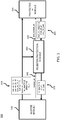
- FIG. 1 is a simplified block diagram of a conventional electronic circuit 100 having a master module 110 that can write data to and read data from the functional registers (not shown in FIG. 1 ) of a hardware IP module 120 via an access bus 115.
- the circuit 100 has a register protection module 130 that prevents the master module 110 from performing unintended write operations to selectively locked functional registers in the protected module 120.
- the master module 110 communicates with the IP module 120 and the protection module 130 via the access bus 115, and the protection module 130 communicates with the IP module 120 via a dedicated bus 125.
- the protection module 130 has a soft lock bit (SLB) register that indicates whether or not write operations to that functional register are enabled.
- each SLB corresponds to an 8-bit (i.e., byte size) functional register.
- the corresponding SLB in the protection module 130 is set ( i.e ., to logic value 1), thereby locking the functional register.
- the corresponding SLB in the protection module 130 is reset (to logic value 0), thereby unlocking the functional register.
- the protection module 130 Whenever the protection module 130 determines that the master module 110 is attempting to write data to a functional register in the IP module 120, the protection module 130 checks the value of the SLB corresponding to that functional register to determine whether or not to allow the write operation to be executed. If the SLB is set, then the protection module 130 determines that the write instructions were unintended and prevents the write operation from being executed. If the SLB is not set, then the protection module 130 assumes that the write instructions were intended and allows the write operation to be executed.
- the master module 110 If and when the master module 110 wants to perform an intentional write operation to a locked functional register, the master module 110 must first send a command to reset the corresponding SLB in the protection module 130 in order to unlock the functional register and then send a command for the write operation to the now-unlocked functional register.
- the protection module 130 will receive and execute the reset command to reset the SLB.
- the protection module 130 will then receive the write command, check the SLB and determine that the functional register is unlocked, and allow the write command to be executed.
- the protection module 130 supports two different types of write operations to the functional registers in the IP module 120: a write-without-lock operation and a write-with-lock operation.
- a write-without-lock operation the protection module 130 allows the master module 110 to write to an unlocked functional register having a reset SLB, where the protection module 130 leaves the SLB reset and the functional register unlocked.
- a write-with-lock operation the protection module 130 allows the master module 110 to write to an unlocked functional register having a reset SLB, where the protection module 130 then automatically sets the SLB, thereby locking the functional register.
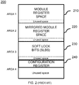
- FIG. 2 is a representation of a conventional memory map 200 of the IP module 120 and the protection module 130 of FIG. 1 .
- the first area represents a module register address space 210 associated with the functional registers in the IP module 120 for the write-without-lock operations.
- the second area represents a mirrored module register address space 220 associated with the functional registers in the IP module 120 for the write-with-lock operations. Note that the address of each functional register in the first area 210 differs from the address of the same functional register in the second area 220 only in one or more of their MSBs (most significant bits). The number of differing MSBs depends on the size of the first and second areas. These MSBs are consumed by the protection module 130 to determine the appropriate area in the memory map 200 and are not sent to the IP module 120.
- the master module 110 uses the address for that functional register in the module register space 210. To request a write-with-lock operation to an unlocked functional register, the master module 110 uses the address for that functional register in the mirrored module register space 220.
- the protection module 130 When the protection module 130 receives a write command to an unlocked functional register, the protection module 130 analyzes the MSBs of the address addr to determine whether the write command is for a write-without-lock operation or a write-with-lock operation.
- the addresses in the module register space 210 are identical to the actual addresses of the functional registers in the IP module 120, so when the address addr for a write command is in the mirrored module register space 220, the protection module 130 translates that address to the corresponding address prot_addr in the module register space 210. Note that, when the address addr is in the module register space 210, no translation is required and the protection module 130 sets prot_addr equal to addr.
- the third area represents the address space 230 associated with the SLBs in the protection module 130
- the fourth area represents the address space 240 associated with a general configuration register (GCR) that stores certain control parameters used by the protection module 130 (e.g ., HLB and UAA as described further below in relation to FIG. 4 ).
- GCR general configuration register
- the size of the address space for the IP module 120 must be preserved in an integer power of two (e.g ., 1KB, 2KB, 4KB, etc .). Assume, for example, that the functional registers in the IP module 120 have a size of 1KB. In that case, 4KB of address space are needed in the memory map 200 to support the 1KB of functional registers, that is, four times the size of the functional registers.
- the sizes of the SLBs and the GCR are smaller than the size of the corresponding functional registers. Additionally, the total address space always needs to be aligned at a 4KB boundary. As such, if the sum of all of the sections of the memory map 200 is less than an integer multiple of 4KB, then padding is added to align the memory map 200 to next integer multiple of 4KB. With the above constraints on functional registers having sizes ranging from 1KB to 32KB, the size of the memory map 200 varies from 4 to 2.4 times the size of the functional registers.
- the memory map would need 8KB of address space: 2KB for the module register space 210, 2KB for the mirrored module register space 220, 0.5KB for the SLBs 230, and 3.5KB for the GCR 240, which is, four times the size of the functional registers.
- the memory map still requires 76KB of address space: 32KB for the module register space 210, 32KB for the mirrored module register space 220, 8KB for the SLBs 230, and 4KB for the GCR 240 or about 2.4 times the size of the functional registers.
- high and low when referring to logic states, mean a high logic value, which typically is a binary one, and a low logic value, which is a binary zero.
- an electronic circuit comprises a protected module having functional registers, a master module that writes/reads data to/from the functional registers, and a protection module that prevents unintended write operations by the master module to the functional registers.
- the protection module includes soft lock bits (SLBs) corresponding to the functional registers, where, if an SLB is set, then the corresponding functional register is locked.
- the protection module also includes control logic that supports (a) a page select (PS) control parameter that indicates whether access by the master module is to the functional registers or to the SLBs and (b) a mode select (MS) control parameter that indicates whether access by the master module to the functional registers is in a normal access mode in which each written-to functional register is left unlocked or an auto-lock access mode in which each written-to functional register is locked by setting the corresponding SLB.
- PS page select
- MS mode select
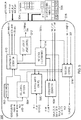
- the electronic circuit 300 has a master module 310, an access bus 315, a protected hardware IP module 320, a dedicated bus 325, and a register protection module 330, all of which are, at a generic functional level, analogous to the corresponding components of the electronic circuit 100.
- the protection module 330 functions to prevent the master module 310 from performing unintended write operations to functional registers in the protected module 320.
- the circuit 300 may comprise a System on a Chip (SOC) having multiple cores, multiple memories, multiple accelerators, and a complex interconnection scheme.
- SOC System on a Chip
- FIG. 3 shows only one master module 310, only one protected module 320, and only one protection module 330
- the electronic circuit 300 may have one or more of each, where, for example, each master module 310 may access more than one protected module 320, each protected module 320 may be accessed by different master modules 310, but by only one master module 310 at a time, and each protection module 330 may protect more than one protected module 320. Note, however, that each protected module 320 is protected by only one protection module 330.
- one difference between the circuit 300 and the conventional circuit 100 is that, in the circuit 300, the addresses used for read and write operations to functional registers in the protected module 320 never need to be translated. As such, the address addr is available on the access bus 315 for use by the protected module 320 as well as by the protection module 330. Note that the width of the addr bus of the access bus 315 in the circuit 300 is 2 bits smaller than the width of the addr bus of the access bus 115 in the circuit 100. As described further below, other differences between the circuit 300 and the conventional circuit 100 exist within the protection module 330.
- the access bus 315 is used to access the protected module 320 and the protection module 330.
- the following signals are transmitted over the access bus 315, in one possible implementation, as shown in FIG. 3 :
- signals shown in FIG. 3 being transmitted on the access bus 315 and the dedicated bus 325 correspond to one possible implementation of the circuit 300. Other implementations may transmit one or more of those signals on different busses and/or one or more other signals on those busses.
- the circuit 300 can be (but does not have to be) provisioned using a conventional master module such as the master module 110 of FIG. 1 for the master module 310 of FIG. 3 and/or a conventional protected module such as the protected module 120 of FIG. 1 for the protected module 320 of FIG. 3 .
- a conventional master module such as the master module 110 of FIG. 1 for the master module 310 of FIG. 3
- a conventional protected module such as the protected module 120 of FIG. 1 for the protected module 320 of FIG. 3
- the software executed by the master module 310 will be different from the software executed by the master module 110 to take into account differences between the protection module 330 and the protection module 130. Note that there need not be any differences between the hardware and the software of the protected modules 120 and 320.
- FIG. 4 is a simplified block diagram showing implementation details for the protected module 320 and for the protection module 330.
- the protection module 330 In addition to the SLBs 332 and the GCR 336, the protection module 330 also has access and protection control logic 338, which controls the operations of the protection module 330.
- the byte-size GCR 336 stores the following five different control parameters:
- An HLB value of 0 implies that all SLBs 332 are accessible and can be modified.
- An HLB value of 1 implies that all SLBs 332 are write protected and cannot be modified by any (software) means. HLB cannot be cleared once it is set; it can be cleared only by a hardware reset.
- a UAA value of 0 implies that the functional registers 322 in the protected module 320 as well as the SLBs 332 and the GCR 336 in the protection module 330 can be written to only in supervisor mode.
- a UAA value of 1 implies that the functional registers 322 in the protected module 320 can be accessed as per the accessibility defined by the protected module 320 along with the SLBs 332 and the GCR 336 in the protection module 330 in both user and supervisor modes.
- the present invention virtually creates two pages in the same address space: (i) a functional register page 324 corresponding to the functional registers 322 in the protected module 320 and (ii) an SLB page 334 corresponding to the SLBs 332 in the protection module 330.
- the PS control parameter selects either the functional page or the SLB page for read and write operations.
- a PS value of 0 implies that the functional register page is selected.
- a PS value of 1 implies that the SLB page is selected. Note that setting and resetting an SLB are essentially two different write operations to the SLB.
- the GCR 336 does not belong to any page. When the GCR 336 is accessed (read or write), the PS value is ignored.
- An MS value of 0 implies that the normal access mode is selected, such that writing to an unlocked functional register 322 leaves the corresponding SLB 332 reset and the functional register 322 unlocked.
- An MS value of 1 implies that the auto-lock access mode is selected, such that writing to an unlocked functional register 322 results in the corresponding SLB 332 being set and the functional register 322 being locked.
- An ASE value of 0 implies that automatic page switching is disabled.
- An ASE value of 1 implies that automatic page switching is enabled.
- the protection module 330 automatically resets the PS control parameter to 0 such that the next command will be issued to a functional register, typically the functional register 322 corresponding to that written (normally reset) SLB 332.
- the protection module 330 automatically sets the PS control parameter to 1 such that the next command can be a command to write (normally reset) another SLB 332.
- the PS control parameter is toggled only during a write command. A read command to either the SLB page or the functional register page or any access to the GCR address does not toggle the PS control parameter. Access to the GCR 336 is PS agnostic.
- FIG. 5 is a simplified block diagram of the protection module 330 of FIGS. 3 and 4 showing implementation details for the control logic 338 of FIG. 4 .
- the access check sub-module 502 validates the access from the master module 310 and generates authentication control for the other sub-modules in the protection module 330.
- the access check sub-module 502 uses signals supervisor_access, rw_b, and module_en from access bus 315, a control parameter UAA from GCR 336.
- An access error is indicated in a write operation if none of the following conditions are met:
- the access mode selection sub-module 504 determines the accessed resources and the access modes.
- the resources are the protected module 320, the GCR 336, and the SLBs 332.
- the access modes for the protected module 320 are the normal access mode and the auto-lock access mode.
- the access mode selection sub-module 504 uses the address bus addr from the access bus 315 and the control parameters PS and MS from the GCR 336.
- the access mode selection sub-module 504 generates control to the access enable generation sub-module 510, the soft lock bit update control sub-module 512, and the read data control sub-module 516 to work.
- the mode is selected on the following conditions:
- the auto page switch control sub-module 506 validates the automatic page switching conditions and helps toggling of the PS control parameter in the GCR 336 at the required instant.
- the auto page switch control sub-module 506 receives input from the access enable generation sub-module 510, the access mode selection sub-module 504, the signals rw_b and xfr_err from the access bus 315, and a control parameter ASE from GCR 336.
- the access error generation sub-module 508 determines that the master module 310 transmitted a write command for a locked functional register 322 by determining that the corresponding SLB 332 is set, the access error generation sub-module 508 prevents the write command from being executed and transmits an error message via the xfr_err signal to the master module 310.
- the access error generation sub-module 508 also provides an error message when the access check sub-module 502 indicates an un-authorized access or any write command for an SLB 332 when the hard lock bit HLB control parameter of the GCR 336 is set.
- the access enable generation sub-module 510 generates the actual enable signals for the protected module 320, the SLBs 332, and the GCR 336.
- the access enable generation sub-module 510 receives inputs from the access check sub-module 502, the access mode selection sub-module 504, and the protection violation check sub-module 514.
- the soft lock bit update control sub-module 512 generates the values of the SLB bits to be updated when a write command is issued by the master module 310 either to write to any protected functional register 322 in the protected module 320 or to write SLB bits at an address to reset or set the SLB 332.
- the soft lock bit update control sub-module 512 receives outputs from the access mode selection sub-module 504 and the access enable generation sub-module 510.
- the protection violation check sub-module 514 detects a protection violation when a write command is issued to a locked functional register 322 by determining that the corresponding SLB 332 is set and indicates this result to the access enable generation sub-module 510 and the access error generation sub-module 508 which disables the prot_module_en signal and generates the access error signal xfr_err to the master module 310, respectively.
- the read data control sub-module 516 generates the read data rd_data of the access bus 315 in response to a read command from the master module 310 based on the page selection parameter PS from the GCR 336 and the addr signal from the access bus 315.
- the read data control sub-module 516 receives inputs from the access enable generation sub-module 510, the GCR 336, the read data output mod rd data from the protected module 320, and the SLB bits 332.
- the corresponding SLB in the protection module 330 is reset and the PS control parameter is automatically toggled to 0, thereby selecting the functional register page.
- a second step data is written to the now-unlocked functional register in the protected module 320, the corresponding SLB is set to re-lock the functional register, and the PS control parameter is automatically toggled back to 1, thereby selecting the SLB page to repeat the process for writing to the next locked functional register, and so on.
- FIG. 10 is a table that describes the different operating modes for the protection module 330 of FIG. 3 for the different combinations of control parameters stored in the GCR 336 of FIG. 4 .
- FIG. 11 is a representation of a memory map 1100 for one possible implementation of the protected module 320 and the protection module 330 of FIG. 3 .
- the memory map 1100 associated with the circuit 300 has only one block of addresses as compared to the memory map 200 of FIG. 2 for the conventional circuit 100 of FIG. 1 , which has four blocks of addresses.
- the addition of the MS control parameter to indicate selection of either the normal access mode or the auto-lock access mode eliminates the need for the mirrored address space 220 of FIG. 2 .
- the addition of the PS control parameter to indicate whether the selected page is the functional register page 324 or the SLB page 334 enables the functional registers and their corresponding SLBs to share the same addresses, thereby eliminating the SLB address space 230 of FIG. 2 .
- the entire memory map 1100 for the protected module 320 and the protection module 330 can be equal to the address space needed for the functional registers plus one additional address for the GCR 336.
- the entire memory map 1100 can be 1KB.
- the entire memory map 1100 can be 2KB.
- the address space for the functional registers is as large as 32KB-4B, then the entire memory map 1100 can be 32KB.
- the circuit 300 is immune to the address space size and does not need the address space of protected module 320 to be aligned to an integer power of 2. For example, if the protected module 320 has 155 address locations, then the circuit 300 can be implemented with 156 address locations, where 155 are for the functional registers and the corresponding SLBs and one is for the GCR.
- each SLB corresponds to an 8-bit functional register
- each SLB can correspond to a functional register having a size equal to 2 n bytes, where n is a non-negative integer.
- a protection module for an electronic circuit prevents unintended write operations by a master module to functional registers of a protected module.
- the protection module includes soft lock bits (SLBs) that indicate whether corresponding functional registers are locked and control logic that supports (i) a page select (PS) control parameter that indicates whether access by the master module is to the functional registers or the SLBs and (ii) a mode select (MS) control parameter that indicates whether access by the master module to the functional registers is in a normal access mode, in which each written-to functional register is left unlocked, or an auto-lock access mode, in which each just-written-to functional register is automatically locked by setting the corresponding SLB.
- the functional registers and the SLBs share addresses that can fit within a single address space that includes the control parameters.
Landscapes
- Engineering & Computer Science (AREA)
- Theoretical Computer Science (AREA)
- Physics & Mathematics (AREA)
- General Engineering & Computer Science (AREA)
- General Physics & Mathematics (AREA)
- Computer Security & Cryptography (AREA)
- Quality & Reliability (AREA)
- Storage Device Security (AREA)
Abstract
Description
- The present invention relates generally to electronic circuits and, more particularly, to techniques for preventing unintended write operations to functional registers of hardware IP modules.
-
FIG. 1 is a simplified block diagram of a conventionalelectronic circuit 100 having amaster module 110 that can write data to and read data from the functional registers (not shown inFIG. 1 ) of ahardware IP module 120 via anaccess bus 115. In addition, thecircuit 100 has aregister protection module 130 that prevents themaster module 110 from performing unintended write operations to selectively locked functional registers in the protectedmodule 120. Themaster module 110 communicates with theIP module 120 and theprotection module 130 via theaccess bus 115, and theprotection module 130 communicates with theIP module 120 via adedicated bus 125. - Although not shown in
FIG. 1 , for each functional register in theIP module 120, theprotection module 130 has a soft lock bit (SLB) register that indicates whether or not write operations to that functional register are enabled. In some implementations, each SLB corresponds to an 8-bit (i.e., byte size) functional register. To protect a functional register in theIP module 120 from an unintended write operation, the corresponding SLB in theprotection module 130 is set (i.e., to logic value 1), thereby locking the functional register. To enable a write operation to a locked functional register in theIP module 120, the corresponding SLB in theprotection module 130 is reset (to logic value 0), thereby unlocking the functional register. - Whenever the
protection module 130 determines that themaster module 110 is attempting to write data to a functional register in theIP module 120, theprotection module 130 checks the value of the SLB corresponding to that functional register to determine whether or not to allow the write operation to be executed. If the SLB is set, then theprotection module 130 determines that the write instructions were unintended and prevents the write operation from being executed. If the SLB is not set, then theprotection module 130 assumes that the write instructions were intended and allows the write operation to be executed. - If and when the
master module 110 wants to perform an intentional write operation to a locked functional register, themaster module 110 must first send a command to reset the corresponding SLB in theprotection module 130 in order to unlock the functional register and then send a command for the write operation to the now-unlocked functional register. Theprotection module 130 will receive and execute the reset command to reset the SLB. Theprotection module 130 will then receive the write command, check the SLB and determine that the functional register is unlocked, and allow the write command to be executed. - The
protection module 130 supports two different types of write operations to the functional registers in the IP module 120: a write-without-lock operation and a write-with-lock operation. In a write-without-lock operation, theprotection module 130 allows themaster module 110 to write to an unlocked functional register having a reset SLB, where theprotection module 130 leaves the SLB reset and the functional register unlocked. In a write-with-lock operation, theprotection module 130 allows themaster module 110 to write to an unlocked functional register having a reset SLB, where theprotection module 130 then automatically sets the SLB, thereby locking the functional register. -
FIG. 2 is a representation of aconventional memory map 200 of theIP module 120 and theprotection module 130 ofFIG. 1 . The first area represents a moduleregister address space 210 associated with the functional registers in theIP module 120 for the write-without-lock operations. The second area represents a mirrored moduleregister address space 220 associated with the functional registers in theIP module 120 for the write-with-lock operations. Note that the address of each functional register in thefirst area 210 differs from the address of the same functional register in thesecond area 220 only in one or more of their MSBs (most significant bits). The number of differing MSBs depends on the size of the first and second areas. These MSBs are consumed by theprotection module 130 to determine the appropriate area in thememory map 200 and are not sent to theIP module 120. - To request a write-without-lock operation to an unlocked functional register in the protected
module 120, themaster module 110 uses the address for that functional register in themodule register space 210. To request a write-with-lock operation to an unlocked functional register, themaster module 110 uses the address for that functional register in the mirroredmodule register space 220. - When the
protection module 130 receives a write command to an unlocked functional register, theprotection module 130 analyzes the MSBs of the address addr to determine whether the write command is for a write-without-lock operation or a write-with-lock operation. For thememory map 200, the addresses in themodule register space 210 are identical to the actual addresses of the functional registers in theIP module 120, so when the address addr for a write command is in the mirroredmodule register space 220, theprotection module 130 translates that address to the corresponding address prot_addr in themodule register space 210. Note that, when the address addr is in themodule register space 210, no translation is required and theprotection module 130 sets prot_addr equal to addr. - Referring again to
FIG. 2 , the third area represents theaddress space 230 associated with the SLBs in theprotection module 130, and the fourth area represents theaddress space 240 associated with a general configuration register (GCR) that stores certain control parameters used by the protection module 130 (e.g., HLB and UAA as described further below in relation toFIG. 4 ). - In a typical implementation of the conventional
electronic circuit 100, the size of the address space for theIP module 120 must be preserved in an integer power of two (e.g., 1KB, 2KB, 4KB, etc.). Assume, for example, that the functional registers in theIP module 120 have a size of 1KB. In that case, 4KB of address space are needed in thememory map 200 to support the 1KB of functional registers, that is, four times the size of the functional registers. - In the
conventional circuit 100, the sizes of the SLBs and the GCR are smaller than the size of the corresponding functional registers. Additionally, the total address space always needs to be aligned at a 4KB boundary. As such, if the sum of all of the sections of thememory map 200 is less than an integer multiple of 4KB, then padding is added to align thememory map 200 to next integer multiple of 4KB. With the above constraints on functional registers having sizes ranging from 1KB to 32KB, the size of thememory map 200 varies from 4 to 2.4 times the size of the functional registers. For example, for functional registers having a size of 2KB, the memory map would need 8KB of address space: 2KB for themodule register space 210, 2KB for the mirroredmodule register space 220, 0.5KB for theSLBs 230, and 3.5KB for theGCR 240, which is, four times the size of the functional registers. For larger and larger functional registers up to 32KB, the memory map still requires 76KB of address space: 32KB for themodule register space 210, 32KB for the mirroredmodule register space 220, 8KB for theSLBs 230, and 4KB for theGCR 240 or about 2.4 times the size of the functional registers. Thus, it would be desirable to have a technique for protecting functional registers from unintended write operations that uses less address space than the conventional technique ofFIGS. 1 and2 . - Embodiments of the present invention are illustrated by way of example and are not limited by the accompanying figures, in which like references indicate similar elements. Elements in the figures are illustrated for simplicity and clarity and have not necessarily been drawn to scale. For example, the thicknesses of layers and regions may be exaggerated for clarity.
-
FIG. 1 is a simplified block diagram of a conventional electronic system; -
FIG. 2 is a representation of a memory map of the IP module and the protection module ofFIG. 1 ; -
FIG. 3 is a simplified block diagram of an electronic circuit according to one embodiment of the present invention; -
FIG. 4 is a simplified block diagram showing implementation details for the IP module and the protection module ofFIG. 3 . -
FIG. 5 is a simplified block diagram of the protection module ofFIGS. 3 and4 showing implementation details for the control logic ofFIG. 4 ; -
FIG. 6 is a representation of the processing involved in writing to an unlocked functional register in the IP module ofFIG. 3 in the normal access mode; -
FIG. 7 is a representation of the processing involved in writing to an unlocked functional register in the IP module ofFIG. 3 in the auto-lock access mode; -
FIG. 8 is a representation of the processing involved in writing to an SLB in the protection module ofFIG. 3 ; -
FIG. 9 is a representation of the processing involved in writing to a sequence of locked functional registers in the IP module ofFIG. 3 with automatic page switching enabled and the auto-lock access mode selected; -
FIG. 10 is a table that shows the different operating modes for the protection module ofFIG. 3 for the different combinations of control parameters stored in the GCR ofFIG. 4 ; and -
FIG. 11 is a representation of a memory map for one possible implementation of the IP module and the protection module ofFIG. 3 . - Detailed illustrative embodiments of the present invention are disclosed herein. However, specific structural and functional details disclosed herein are merely representative for purposes of describing example embodiments of the present invention. Embodiments of the present invention may be embodied in many alternative forms and should not be construed as limited to only the embodiments set forth herein. Further, the terminology used herein is for the purpose of describing particular embodiments only and is not intended to be limiting of example embodiments of the invention.
- As used herein, the singular forms "a", "an", and "the", are intended to include the plural forms as well, unless the context clearly indicates otherwise. It further will be understood that the terms "comprises", "comprising", "has", "having", "includes", or "including" specify the presence of stated features, steps, or components, but do not preclude the presence or addition of one or more other features, steps, or components. It also should be noted that, in some alternative implementations, the functions/acts noted might occur out of the order noted in the figures. For example, two figures shown in succession may in fact be executed substantially concurrently or may sometimes be executed in the reverse order, depending upon the functionality/acts involved. The term "or" is to be interpreted as inclusive unless indicated otherwise.
- The terms "high" and "low", when referring to logic states, mean a high logic value, which typically is a binary one, and a low logic value, which is a binary zero.
- According to certain embodiments of the present invention, an electronic circuit comprises a protected module having functional registers, a master module that writes/reads data to/from the functional registers, and a protection module that prevents unintended write operations by the master module to the functional registers. The protection module includes soft lock bits (SLBs) corresponding to the functional registers, where, if an SLB is set, then the corresponding functional register is locked. The protection module also includes control logic that supports (a) a page select (PS) control parameter that indicates whether access by the master module is to the functional registers or to the SLBs and (b) a mode select (MS) control parameter that indicates whether access by the master module to the functional registers is in a normal access mode in which each written-to functional register is left unlocked or an auto-lock access mode in which each written-to functional register is locked by setting the corresponding SLB.
- Referring now to
FIG. 3 , a simplified block diagram of anelectronic circuit 300 according to one embodiment of the present invention is shown. Like the conventionalelectronic circuit 100 ofFIG. 1 , theelectronic circuit 300 has amaster module 310, anaccess bus 315, a protectedhardware IP module 320, adedicated bus 325, and aregister protection module 330, all of which are, at a generic functional level, analogous to the corresponding components of theelectronic circuit 100. In particular, like theprotection module 130 ofFIG. 1 , theprotection module 330 functions to prevent themaster module 310 from performing unintended write operations to functional registers in the protectedmodule 320. Thecircuit 300 may comprise a System on a Chip (SOC) having multiple cores, multiple memories, multiple accelerators, and a complex interconnection scheme. - Although
FIG. 3 shows only onemaster module 310, only one protectedmodule 320, and only oneprotection module 330, in general, theelectronic circuit 300 may have one or more of each, where, for example, eachmaster module 310 may access more than one protectedmodule 320, each protectedmodule 320 may be accessed bydifferent master modules 310, but by only onemaster module 310 at a time, and eachprotection module 330 may protect more than one protectedmodule 320. Note, however, that each protectedmodule 320 is protected by only oneprotection module 330. - As indicated in
FIG. 3 and as described in further detail below, one difference between thecircuit 300 and theconventional circuit 100 is that, in thecircuit 300, the addresses used for read and write operations to functional registers in the protectedmodule 320 never need to be translated. As such, the address addr is available on theaccess bus 315 for use by the protectedmodule 320 as well as by theprotection module 330. Note that the width of the addr bus of theaccess bus 315 in thecircuit 300 is 2 bits smaller than the width of the addr bus of theaccess bus 115 in thecircuit 100. As described further below, other differences between thecircuit 300 and theconventional circuit 100 exist within theprotection module 330. - The
access bus 315 is used to access the protectedmodule 320 and theprotection module 330. The following signals are transmitted over theaccess bus 315, in one possible implementation, as shown inFIG. 3 : - One-bit module enable signal module_en indicates whether the protected
module 320 or theprotection module 330 is being accessed; - One-bit byte enable signals byte_en_31_24, byte_en_23_16, byte_en_15_8, and byte_en_7_0 enable individual byte selection during an access;
- One-bit supervisor access signal supervisor_access indicates whether supervisor or user access is selected;
- Data to be written wr_data is provided by a 32-bit write data bus;
- Address addr[n-1:0] is provided via an n-bit address bus;
- One-bit read and write bar signal rw_b indicates access type (e.g., 1=read, 0=write);
- Read data rd_data is provided by a 32-bit read data bus;
- One-bit transfer error signal xfr_err indicates whether the access is invalid and no write or read operation is performed; and
- One-bit transfer wait signal xfr_wait indicates whether access cannot be completed in the current clock cycle.
- Note that the signals shown in
FIG. 3 being transmitted on theaccess bus 315 and thededicated bus 325 correspond to one possible implementation of thecircuit 300. Other implementations may transmit one or more of those signals on different busses and/or one or more other signals on those busses. - In certain implementations, the
circuit 300 can be (but does not have to be) provisioned using a conventional master module such as themaster module 110 ofFIG. 1 for themaster module 310 ofFIG. 3 and/or a conventional protected module such as the protectedmodule 120 ofFIG. 1 for the protectedmodule 320 ofFIG. 3 . Although there need not be any hardware differences between themaster module 310 and themaster module 110, the software executed by themaster module 310 will be different from the software executed by themaster module 110 to take into account differences between theprotection module 330 and theprotection module 130. Note that there need not be any differences between the hardware and the software of the protectedmodules -
FIG. 4 is a simplified block diagram showing implementation details for the protectedmodule 320 and for theprotection module 330. - As shown in
FIG. 4 , the protectedmodule 320 has up to 2 n+2-4 byte-sizefunctional registers 322 in a functionalmodule address page 324 having addresses that range from 0 to 2 n -2, where n is an integer and there are four different byte-sizefunctional registers 322 at each address location. Theprotection module 330 has up to 2 n+2-4SLBs 332 in anSLB address page 334 having the same addresses ranging from 0 to 2 n -2, where there are four different 1-bit SLBs 332 at each address location, and eachSLB 332 has the same address as its correspondingfunctional register 322. - The reason why there are only 2 n -1 addresses in the functional module and
SLB pages protection module 330 stores its control parameters in aGCR 336 at address 2 n -1, so that the memory map for thefunctional registers 322, theSLBs 332, and theGCR 336 can all share a single block of 2 n addresses. Note that, in other implementations, a different address can be used for theGCR 336. - In addition to the
SLBs 332 and theGCR 336, theprotection module 330 also has access andprotection control logic 338, which controls the operations of theprotection module 330. - As shown in
FIG. 4 , the byte-size GCR 336 stores the following five different control parameters: - 1-bit Hard Lock Bit (HLB) Control Parameter;
- 1-bit User Access Allowed (UAA) Control Parameter;
- 1-bit Mode Select (MS) Control Parameter;
- 1-bit Page Select (PS) Control Parameter; and
- 1-bit Automatic Page Switching Enable (ASE) Control Parameter.
- An HLB value of 0 implies that all
SLBs 332 are accessible and can be modified. An HLB value of 1 implies that allSLBs 332 are write protected and cannot be modified by any (software) means. HLB cannot be cleared once it is set; it can be cleared only by a hardware reset. - A UAA value of 0 implies that the
functional registers 322 in the protectedmodule 320 as well as theSLBs 332 and theGCR 336 in theprotection module 330 can be written to only in supervisor mode. A UAA value of 1 implies that thefunctional registers 322 in the protectedmodule 320 can be accessed as per the accessibility defined by the protectedmodule 320 along with theSLBs 332 and theGCR 336 in theprotection module 330 in both user and supervisor modes. - The present invention virtually creates two pages in the same address space: (i) a
functional register page 324 corresponding to thefunctional registers 322 in the protectedmodule 320 and (ii) anSLB page 334 corresponding to theSLBs 332 in theprotection module 330. The PS control parameter selects either the functional page or the SLB page for read and write operations. A PS value of 0 implies that the functional register page is selected. A PS value of 1 implies that the SLB page is selected. Note that setting and resetting an SLB are essentially two different write operations to the SLB. TheGCR 336 does not belong to any page. When theGCR 336 is accessed (read or write), the PS value is ignored. - The MS control parameter selects the access mode when the functional register page is the selected page (i.e., PS=0). An MS value of 0 implies that the normal access mode is selected, such that writing to an unlocked
functional register 322 leaves thecorresponding SLB 332 reset and thefunctional register 322 unlocked. An MS value of 1 implies that the auto-lock access mode is selected, such that writing to an unlockedfunctional register 322 results in thecorresponding SLB 332 being set and thefunctional register 322 being locked. When either the SLB page (i.e., PS=1) or theGCR 336 is accessed, the MS value is ignored. - An ASE value of 0 implies that automatic page switching is disabled. An ASE value of 1 implies that automatic page switching is enabled. As described further below in the context of
FIG. 9 , if automatic page switching is enabled, then, whenever anSLB 332 is written (normally reset), theprotection module 330 automatically resets the PS control parameter to 0 such that the next command will be issued to a functional register, typically thefunctional register 322 corresponding to that written (normally reset)SLB 332. In addition, with automatic page switching enabled, whenever a write command to afunctional register 322 is executed, theprotection module 330 automatically sets the PS control parameter to 1 such that the next command can be a command to write (normally reset) anotherSLB 332. The PS control parameter is toggled only during a write command. A read command to either the SLB page or the functional register page or any access to the GCR address does not toggle the PS control parameter. Access to theGCR 336 is PS agnostic. - Automatic page switching reduces the number of commands required to write to a previously locked
functional register 322 from four commands to only two commands. If automatic page switching is disabled (ASE=0), in order to write to a previously locked functional register 322 (after having just written data to a different unlocked functional register 322), the following four commands are executed: - Command No. 1: Set PS=1 to select SLB page;
- Command No. 2: Reset the
corresponding SLB 332 to unlock thefunctional register 322; - Command No. 3: Set PS=0 to select the functional register page; and
- Command No. 4: Write data to the unlocked
functional register 322. - If, however, automatic page switching is enabled (ASE=1), in order to write to a previously locked functional register 322 (after having just written data to a different unlocked functional register 322), only the following two commands are executed:
- Command No. 1: Reset the
corresponding SLB 332 to unlock thefunctional register 322 after which PS is automatically reset to 0 to select the functional register page; and - Command No. 2: Write data to the unlocked
functional register 322 after which PS is automatically set to 1 to select the SLB page. -
FIG. 5 is a simplified block diagram of theprotection module 330 ofFIGS. 3 and4 showing implementation details for thecontrol logic 338 ofFIG. 4 . - The
access check sub-module 502 validates the access from themaster module 310 and generates authentication control for the other sub-modules in theprotection module 330. Theaccess check sub-module 502 uses signals supervisor_access, rw_b, and module_en fromaccess bus 315, a control parameter UAA fromGCR 336. - An access error is indicated in a write operation if none of the following conditions are met:
- 1) Access is in supervisor mode (i.e., supervisor_access is 1)
- 2) Access is in user mode (i.e., supervisor_access is 0) but user access is allowed (i.e., the control parameter UAA is 1)
- The access
mode selection sub-module 504 determines the accessed resources and the access modes. The resources are the protectedmodule 320, theGCR 336, and theSLBs 332. The access modes for the protectedmodule 320 are the normal access mode and the auto-lock access mode. The accessmode selection sub-module 504 uses the address bus addr from theaccess bus 315 and the control parameters PS and MS from theGCR 336. The accessmode selection sub-module 504 generates control to the access enable generation sub-module 510, the soft lock bitupdate control sub-module 512, and the read data control sub-module 516 to work. The mode is selected on the following conditions: - 1) The auto-lock access mode is declared when PS=0, MS=1, and the
master module 310 is not accessing theGCR 336. - 2) The normal access mode is declared when PS=0, MS=0, and the
master module 310 is not accessing theGCR 336. - The auto page
switch control sub-module 506 validates the automatic page switching conditions and helps toggling of the PS control parameter in theGCR 336 at the required instant. The auto pageswitch control sub-module 506 receives input from the access enable generation sub-module 510, the accessmode selection sub-module 504, the signals rw_b and xfr_err from theaccess bus 315, and a control parameter ASE fromGCR 336. - When the access
error generation sub-module 508 determines that themaster module 310 transmitted a write command for a lockedfunctional register 322 by determining that thecorresponding SLB 332 is set, the accesserror generation sub-module 508 prevents the write command from being executed and transmits an error message via the xfr_err signal to themaster module 310. The access error generation sub-module 508 also provides an error message when the access check sub-module 502 indicates an un-authorized access or any write command for anSLB 332 when the hard lock bit HLB control parameter of theGCR 336 is set. - The access enable generation sub-module 510 generates the actual enable signals for the protected
module 320, theSLBs 332, and theGCR 336. The access enable generation sub-module 510 receives inputs from the access check sub-module 502, the accessmode selection sub-module 504, and the protectionviolation check sub-module 514. - The soft lock bit
update control sub-module 512 generates the values of the SLB bits to be updated when a write command is issued by themaster module 310 either to write to any protectedfunctional register 322 in the protectedmodule 320 or to write SLB bits at an address to reset or set theSLB 332. The soft lock bitupdate control sub-module 512 receives outputs from the accessmode selection sub-module 504 and the access enablegeneration sub-module 510. - The protection
violation check sub-module 514 detects a protection violation when a write command is issued to a lockedfunctional register 322 by determining that thecorresponding SLB 332 is set and indicates this result to the access enable generation sub-module 510 and the access error generation sub-module 508 which disables the prot_module_en signal and generates the access error signal xfr_err to themaster module 310, respectively. - The read
data control sub-module 516 generates the read data rd_data of theaccess bus 315 in response to a read command from themaster module 310 based on the page selection parameter PS from theGCR 336 and the addr signal from theaccess bus 315. The readdata control sub-module 516 receives inputs from the access enable generation sub-module 510, theGCR 336, the read data output mod rd data from the protectedmodule 320, and theSLB bits 332. -
FIG. 6 is a representation of the processing involved in writing to an unlocked functional register in the protected module 320 (i.e., PS=0) in the normal access mode (i.e., MS=0). In that case, data is written to the functional register without setting the corresponding SLB in theprotection module 330. -
FIG. 7 is a representation of the processing involved in writing to an unlocked functional register in the protected module 320 (i.e., PS=0) in the auto-lock access mode (i.e., MS=1). In that case, after data is written to the functional register, the corresponding SLB in theprotection module 330 is set to lock the functional register. -
FIG. 8 is a representation of the processing involved in writing to (i.e., setting or resetting) an SLB in the protection module 330 (i.e., PS=1). In that case, a 1 or a 0 is written to the SLB. -
FIG. 9 is a representation of the processing involved in writing to a sequence of locked functional registers in the protectedmodule 320 with automatic page switching enabled (i.e., ASE=1) and the auto-lock access mode selected (i.e., MS=1). In that case, in a first step for any locked functional register, with the SLB page selected (i.e., PS=1), the corresponding SLB in theprotection module 330 is reset and the PS control parameter is automatically toggled to 0, thereby selecting the functional register page. In a second step, data is written to the now-unlocked functional register in the protectedmodule 320, the corresponding SLB is set to re-lock the functional register, and the PS control parameter is automatically toggled back to 1, thereby selecting the SLB page to repeat the process for writing to the next locked functional register, and so on. - Note that, if automatic page switching is enabled (i.e., ASE=1) and the normal access mode is selected (i.e., MS=0), then the processing will be the same as that shown in
FIG. 9 , except that the SLB for the just-written-to functional register will not be automatically set, thereby leaving the functional register unlocked. -
FIG. 10 is a table that describes the different operating modes for theprotection module 330 ofFIG. 3 for the different combinations of control parameters stored in theGCR 336 ofFIG. 4 . -
FIG. 11 is a representation of amemory map 1100 for one possible implementation of the protectedmodule 320 and theprotection module 330 ofFIG. 3 . As represented inFIG. 11 , thememory map 1100 associated with thecircuit 300 has only one block of addresses as compared to thememory map 200 ofFIG. 2 for theconventional circuit 100 ofFIG. 1 , which has four blocks of addresses. - Three different features of the
circuit 300 enable the relative reduced size of thememory map 1100. First, the addition of the MS control parameter to indicate selection of either the normal access mode or the auto-lock access mode eliminates the need for the mirroredaddress space 220 ofFIG. 2 . Second, the addition of the PS control parameter to indicate whether the selected page is thefunctional register page 324 or theSLB page 334 enables the functional registers and their corresponding SLBs to share the same addresses, thereby eliminating theSLB address space 230 ofFIG. 2 . Third, limiting the maximum size of the functional registers in order to reserve one address for theGCR 336 eliminates the need for theGCR address space 240 ofFIG. 2 . - As a result, the
entire memory map 1100 for the protectedmodule 320 and theprotection module 330 can be equal to the address space needed for the functional registers plus one additional address for theGCR 336. For example, if the functional registers are limited to an address space of 1KB-4B, then theentire memory map 1100 can be 1KB. If the functional registers are limited to an address space of 2KB-4B, then theentire memory map 1100 can be 2KB. And if the address space for the functional registers is as large as 32KB-4B, then theentire memory map 1100 can be 32KB. - The
circuit 300 is immune to the address space size and does not need the address space of protectedmodule 320 to be aligned to an integer power of 2. For example, if the protectedmodule 320 has 155 address locations, then thecircuit 300 can be implemented with 156 address locations, where 155 are for the functional registers and the corresponding SLBs and one is for the GCR. - Although the invention has been described in the context of electronic systems in which each SLB corresponds to an 8-bit functional register, in general, each SLB can correspond to a functional register having a size equal to 2 n bytes, where n is a non-negative integer.
- A protection module for an electronic circuit prevents unintended write operations by a master module to functional registers of a protected module. The protection module includes soft lock bits (SLBs) that indicate whether corresponding functional registers are locked and control logic that supports (i) a page select (PS) control parameter that indicates whether access by the master module is to the functional registers or the SLBs and (ii) a mode select (MS) control parameter that indicates whether access by the master module to the functional registers is in a normal access mode, in which each written-to functional register is left unlocked, or an auto-lock access mode, in which each just-written-to functional register is automatically locked by setting the corresponding SLB. The functional registers and the SLBs share addresses that can fit within a single address space that includes the control parameters.
- Although the invention is described herein with reference to specific embodiments, various modifications and changes can be made without departing from the scope of the present invention as set forth in the claims below. Accordingly, the specification and figures are to be regarded in an illustrative rather than a restrictive sense, and all such modifications are intended to be included within the scope of the present invention. Any benefits, advantages, or solutions to problems that are described herein with regard to specific embodiments are not intended to be construed as a critical, required, or essential feature or element of any or all the claims.
- It should be understood that the steps of the exemplary methods set forth herein are not necessarily required to be performed in the order described, and the order of the steps of such methods should be understood to be merely exemplary. Likewise, additional steps may be included in such methods, and certain steps may be omitted or combined, in methods consistent with various embodiments of the invention.
- Although the elements in the following method claims, if any, are recited in a particular sequence with corresponding labeling, unless the claim recitations otherwise imply a particular sequence for implementing some or all of those elements, those elements are not necessarily intended to be limited to being implemented in that particular sequence.
- Reference herein to "one embodiment" or "an embodiment" means that a particular feature, structure, or characteristic described in connection with the embodiment can be included in at least one embodiment of the invention. The appearances of the phrase "in one embodiment" in various places in the specification are not necessarily all referring to the same embodiment, nor are separate or alternative embodiments necessarily mutually exclusive of other embodiments. The same applies to the term "implementation."
Claims (14)
- An electronic circuit, comprising:a protected module having functional registers;a master module that writes data to and reads data from the functional registers; anda protection module that prevents unintended write operations by the master module to the functional registers, wherein the protection module comprises:soft lock bits (SLBs) corresponding to the functional registers, wherein, if an SLB is set, then the corresponding functional register is locked; andcontrol logic that supports:a page select (PS) control parameter that indicates whether access by the master module is to the functional registers or to the SLBs; anda mode select (MS) control parameter that indicates whether access by the master module to the functional registers is in a normal access mode in which each written-to functional register is left unlocked or an auto-lock access mode in which each written-to functional register is locked by setting the corresponding SLB.
- The circuit of claim 1, wherein:each functional register has a single address for both the normal access mode and the auto-lock access mode; andthe address for each functional register is the same as the address for its corresponding SLB.
- The circuit of claim 2, wherein:the addresses for the functional registers and the SLBs fit into an integer number of address blocks; andan address in the integer number of address blocks is used for a general configuration register (GCR) that stores the PS and MS control parameters.
- The circuit of any preceding claim, wherein the PS and MS control parameters are one-bit values.
- The circuit of any preceding claim, wherein the control logic supports an automatic page switching enable (ASE) control parameter that indicates whether the PS control parameter is automatically toggled to the functional registers after a write operation to an SLB and to the SLBs after a write operation to a functional register.
- The circuit of claim 5, wherein the ASE control parameter is a one-bit value.
- The circuit of any preceding claim, wherein:the master module, the protected module, and the protection module communicate via an access bus; andthe protected module and the protection module communicate via a dedicated bus, wherein the master module transmits the address of a functional register to be written to via the access bus.
- The circuit of claim 7, wherein no address translation is performed for the master module to write to a functional register in either the normal access mode or the auto-lock access mode.
- The circuit of any preceding claim, wherein a memory map for the protection module and the protected module comprises a single address space for both the functional registers in the auto-lock access mode and the functional registers in the normal access mode.
- The circuit of claim 9, wherein each functional register and its corresponding SLB have a common address in the single address space of the memory map.
- The circuit of claim 10, wherein the single address space of the memory map further comprises an address for a GCR that stores the control parameters for the control logic.
- The circuit of any preceding claim, wherein the protected module is operable with a protection module that does not support the PS and MS control parameters.
- The circuit of any preceding claim, wherein:each functional register has a single address for both the normal access mode and the auto-lock access mode;the address for each functional register is the same as the address for its corresponding SLB;the addresses for the functional registers and the SLBs fit into an integer number of address blocks;the control logic further supports an automatic page switching enable (ASE) control parameter that indicates whether or not the PS control parameter is automatically toggled to the functional registers after a write operation to an SLB and to the SLBs after a write operation to a functional register;an address in the integer number of address blocks is used for a general configuration register (GCR) that stores the PS, MS, and ASE control parameters;the PS, MS, and ASE control parameters are one-bit values;the master module, the protected module, and the protection module communicate via an access bus of the system;the protected module and the protection module communicate via a dedicated bus, wherein the master module transmits the address of a functional register to be accessed via the access bus;no address translation is performed for the master module to write to a functional register in either the normal access mode or the auto-lock access mode;a memory map for the protection module and the protected module comprises a single address space for both the functional registers in the auto-lock access mode and the functional registers in the normal access mode;each functional register and its corresponding SLB have a common address in the single address space of the memory map;the single address space of the memory map further comprises an address for a GCR that stores the control parameters for the control logic;
- The circuit of claim 13, wherein:
the protected module is operable with a protection module that does not support the PS and MS control parameters.
Applications Claiming Priority (1)
| Application Number | Priority Date | Filing Date | Title |
|---|---|---|---|
| US16/392,427 US10839877B1 (en) | 2019-04-23 | 2019-04-23 | Register protection circuit for hardware IP modules |
Publications (2)
| Publication Number | Publication Date |
|---|---|
| EP3731102A1 true EP3731102A1 (en) | 2020-10-28 |
| EP3731102B1 EP3731102B1 (en) | 2022-08-17 |
Family
ID=70289598
Family Applications (1)
| Application Number | Title | Priority Date | Filing Date |
|---|---|---|---|
| EP20169479.1A Active EP3731102B1 (en) | 2019-04-23 | 2020-04-14 | Register protection circuit for hardware ip modules |
Country Status (2)
| Country | Link |
|---|---|
| US (1) | US10839877B1 (en) |
| EP (1) | EP3731102B1 (en) |
Cited By (1)
| Publication number | Priority date | Publication date | Assignee | Title |
|---|---|---|---|---|
| IT202200002960A1 (en) * | 2022-02-17 | 2023-08-17 | St Microelectronics Srl | Processing system, related integrated circuit, device and process |
Families Citing this family (2)
| Publication number | Priority date | Publication date | Assignee | Title |
|---|---|---|---|---|
| US11354172B2 (en) * | 2020-09-01 | 2022-06-07 | Nxp Usa, Inc. | Centralized access control circuit for controlling access to peripherals |
| FR3158816A1 (en) * | 2024-01-26 | 2025-08-01 | Stmicroelectronics International N.V. | Data write protection |
Citations (2)
| Publication number | Priority date | Publication date | Assignee | Title |
|---|---|---|---|---|
| US20090103362A1 (en) * | 2007-10-17 | 2009-04-23 | Micron Technology, Inc. | System and method for setting access and modification for synchronous serial interface nand |
| US20120072734A1 (en) * | 2010-09-22 | 2012-03-22 | Wishman Allen R | Platform firmware armoring technology |
Family Cites Families (21)
| Publication number | Priority date | Publication date | Assignee | Title |
|---|---|---|---|---|
| US4777588A (en) * | 1985-08-30 | 1988-10-11 | Advanced Micro Devices, Inc. | General-purpose register file optimized for intraprocedural register allocation, procedure calls, and multitasking performance |
| JPH0353328A (en) * | 1989-07-20 | 1991-03-07 | Hitachi Ltd | Register save and recovery method and processing device |
| US5592641A (en) * | 1993-06-30 | 1997-01-07 | Intel Corporation | Method and device for selectively locking write access to blocks in a memory array using write protect inputs and block enabled status |
| US5568380A (en) * | 1993-08-30 | 1996-10-22 | International Business Machines Corporation | Shadow register file for instruction rollback |
| US6026479A (en) * | 1998-04-22 | 2000-02-15 | Hewlett-Packard Company | Apparatus and method for efficient switching of CPU mode between regions of high instruction level parallism and low instruction level parallism in computer programs |
| US6339823B1 (en) * | 1999-07-20 | 2002-01-15 | Ip-First, L.L.C. | Method and apparatus for selective writing of incoherent MMX registers |
| US6779099B2 (en) | 2001-07-20 | 2004-08-17 | Chien-Tzu Hou | Operation method for controlling access attributes of a memorized page of a memory unit and its structure |
| US7302589B2 (en) | 2002-02-20 | 2007-11-27 | Intel Corporation | Method for securing memory mapped control registers |
| KR100532442B1 (en) * | 2003-06-17 | 2005-11-30 | 삼성전자주식회사 | Data processing method and data processing apparatus |
| GB0519363D0 (en) * | 2005-09-22 | 2005-11-02 | Advanced Risc Mach Ltd | Error propagation in integrated circuits |
| US7861093B2 (en) | 2006-08-30 | 2010-12-28 | International Business Machines Corporation | Managing data access via a loop only if changed locking facility |
| US20080263256A1 (en) * | 2007-04-20 | 2008-10-23 | Motorola, Inc. | Logic Device with Write Protected Memory Management Unit Registers |
| DE102007024737A1 (en) * | 2007-05-25 | 2008-11-27 | Robert Bosch Gmbh | Data transfer method between master and slave devices |
| US8041912B2 (en) * | 2007-09-28 | 2011-10-18 | Macronix International Co., Ltd. | Memory devices with data protection |
| JP2011008316A (en) * | 2009-06-23 | 2011-01-13 | Seiko Epson Corp | Information processing device, image display device, and information processing method |
| CN104025026B (en) | 2011-12-29 | 2019-07-26 | 英特尔公司 | Configuration and status register of the access for configuration space |
| US9477482B2 (en) * | 2013-09-26 | 2016-10-25 | Nvidia Corporation | System, method, and computer program product for implementing multi-cycle register file bypass |
| US10007522B2 (en) * | 2014-05-20 | 2018-06-26 | Nxp Usa, Inc. | System and method for selectively allocating entries at a branch target buffer |
| CN105138929B (en) | 2015-10-09 | 2019-05-07 | 天津国芯科技有限公司 | A kind of register guard method and device with anti-error write operation |
| JP6453492B1 (en) * | 2018-01-09 | 2019-01-16 | ウィンボンド エレクトロニクス コーポレーション | Semiconductor memory device |
| US10802754B2 (en) * | 2018-03-12 | 2020-10-13 | Micron Technology, Inc. | Hardware-based power management integrated circuit register file write protection |
-
2019
- 2019-04-23 US US16/392,427 patent/US10839877B1/en active Active
-
2020
- 2020-04-14 EP EP20169479.1A patent/EP3731102B1/en active Active
Patent Citations (2)
| Publication number | Priority date | Publication date | Assignee | Title |
|---|---|---|---|---|
| US20090103362A1 (en) * | 2007-10-17 | 2009-04-23 | Micron Technology, Inc. | System and method for setting access and modification for synchronous serial interface nand |
| US20120072734A1 (en) * | 2010-09-22 | 2012-03-22 | Wishman Allen R | Platform firmware armoring technology |
Cited By (3)
| Publication number | Priority date | Publication date | Assignee | Title |
|---|---|---|---|---|
| IT202200002960A1 (en) * | 2022-02-17 | 2023-08-17 | St Microelectronics Srl | Processing system, related integrated circuit, device and process |
| EP4231161A1 (en) * | 2022-02-17 | 2023-08-23 | STMicroelectronics S.r.l. | A processing system, related integrated circuit, device and method |
| US12117942B2 (en) | 2022-02-17 | 2024-10-15 | Stmicroelectronics S.R.L. | Processing system, related integrated circuit, device and method |
Also Published As
| Publication number | Publication date |
|---|---|
| EP3731102B1 (en) | 2022-08-17 |
| US20200342924A1 (en) | 2020-10-29 |
| US10839877B1 (en) | 2020-11-17 |
Similar Documents
| Publication | Publication Date | Title |
|---|---|---|
| US4163280A (en) | Address management system | |
| EP3731102B1 (en) | Register protection circuit for hardware ip modules | |
| US8955062B2 (en) | Method and system for permitting access to resources based on instructions of a code tagged with an identifier assigned to a domain | |
| US4819232A (en) | Fault-tolerant multiprocessor arrangement | |
| US20140173236A1 (en) | Secure computer system for preventing access requests to portions of system memory by peripheral devices and/or processor cores | |
| JP2006521637A (en) | Memory management in data processing systems | |
| JP5582971B2 (en) | Memory protection method and information processing apparatus | |
| US20180217752A1 (en) | Flash controller and control method for flash controller | |
| JPS63231550A (en) | Multiple virtual space control method | |
| JPS6142306B2 (en) | ||
| US20240380731A1 (en) | System on chip firewall memory architecture | |
| US11354172B2 (en) | Centralized access control circuit for controlling access to peripherals | |
| US20110219219A1 (en) | Semiconductor integrated circuit and register address controller | |
| JP2001117855A (en) | Bus interface circuit creation device and recording medium | |
| JPS59214952A (en) | Processing system of fault | |
| JPH08235073A (en) | Microcomputer | |
| JPH06214890A (en) | calculator | |
| JPS6329859A (en) | Memory protection circuit | |
| US7263623B1 (en) | Microprocessor system | |
| US5983311A (en) | Sequential memory accessing circuit and method of addressing two memory units using common pointer circuit | |
| JP3401729B2 (en) | Split bus control circuit | |
| JP2684752B2 (en) | Extended storage control method | |
| JP3310482B2 (en) | Microcomputer | |
| JPH02302855A (en) | Memory control system | |
| JPH02238536A (en) | Storage protecting circuit |
Legal Events
| Date | Code | Title | Description |
|---|---|---|---|
| PUAI | Public reference made under article 153(3) epc to a published international application that has entered the european phase |
Free format text: ORIGINAL CODE: 0009012 |
|
| STAA | Information on the status of an ep patent application or granted ep patent |
Free format text: STATUS: THE APPLICATION HAS BEEN PUBLISHED |
|
| AK | Designated contracting states |
Kind code of ref document: A1 Designated state(s): AL AT BE BG CH CY CZ DE DK EE ES FI FR GB GR HR HU IE IS IT LI LT LU LV MC MK MT NL NO PL PT RO RS SE SI SK SM TR |
|
| AX | Request for extension of the european patent |
Extension state: BA ME |
|
| STAA | Information on the status of an ep patent application or granted ep patent |
Free format text: STATUS: REQUEST FOR EXAMINATION WAS MADE |
|
| 17P | Request for examination filed |
Effective date: 20210428 |
|
| RBV | Designated contracting states (corrected) |
Designated state(s): AL AT BE BG CH CY CZ DE DK EE ES FI FR GB GR HR HU IE IS IT LI LT LU LV MC MK MT NL NO PL PT RO RS SE SI SK SM TR |
|
| STAA | Information on the status of an ep patent application or granted ep patent |
Free format text: STATUS: EXAMINATION IS IN PROGRESS |
|
| 17Q | First examination report despatched |
Effective date: 20220316 |
|
| GRAP | Despatch of communication of intention to grant a patent |
Free format text: ORIGINAL CODE: EPIDOSNIGR1 |
|
| STAA | Information on the status of an ep patent application or granted ep patent |
Free format text: STATUS: GRANT OF PATENT IS INTENDED |
|
| INTG | Intention to grant announced |
Effective date: 20220421 |
|
| GRAS | Grant fee paid |
Free format text: ORIGINAL CODE: EPIDOSNIGR3 |
|
| GRAA | (expected) grant |
Free format text: ORIGINAL CODE: 0009210 |
|
| STAA | Information on the status of an ep patent application or granted ep patent |
Free format text: STATUS: THE PATENT HAS BEEN GRANTED |
|
| AK | Designated contracting states |
Kind code of ref document: B1 Designated state(s): AL AT BE BG CH CY CZ DE DK EE ES FI FR GB GR HR HU IE IS IT LI LT LU LV MC MK MT NL NO PL PT RO RS SE SI SK SM TR |
|
| REG | Reference to a national code |
Ref country code: CH Ref legal event code: EP |
|
| REG | Reference to a national code |
Ref country code: DE Ref legal event code: R096 Ref document number: 602020004524 Country of ref document: DE |
|
| REG | Reference to a national code |
Ref country code: IE Ref legal event code: FG4D |
|
| REG | Reference to a national code |
Ref country code: AT Ref legal event code: REF Ref document number: 1512634 Country of ref document: AT Kind code of ref document: T Effective date: 20220915 |
|
| REG | Reference to a national code |
Ref country code: NL Ref legal event code: MP Effective date: 20220817 |
|
| REG | Reference to a national code |
Ref country code: LT Ref legal event code: MG9D |
|
| PG25 | Lapsed in a contracting state [announced via postgrant information from national office to epo] |
Ref country code: SE Free format text: LAPSE BECAUSE OF FAILURE TO SUBMIT A TRANSLATION OF THE DESCRIPTION OR TO PAY THE FEE WITHIN THE PRESCRIBED TIME-LIMIT Effective date: 20220817 Ref country code: RS Free format text: LAPSE BECAUSE OF FAILURE TO SUBMIT A TRANSLATION OF THE DESCRIPTION OR TO PAY THE FEE WITHIN THE PRESCRIBED TIME-LIMIT Effective date: 20220817 Ref country code: PT Free format text: LAPSE BECAUSE OF FAILURE TO SUBMIT A TRANSLATION OF THE DESCRIPTION OR TO PAY THE FEE WITHIN THE PRESCRIBED TIME-LIMIT Effective date: 20221219 Ref country code: NO Free format text: LAPSE BECAUSE OF FAILURE TO SUBMIT A TRANSLATION OF THE DESCRIPTION OR TO PAY THE FEE WITHIN THE PRESCRIBED TIME-LIMIT Effective date: 20221117 Ref country code: NL Free format text: LAPSE BECAUSE OF FAILURE TO SUBMIT A TRANSLATION OF THE DESCRIPTION OR TO PAY THE FEE WITHIN THE PRESCRIBED TIME-LIMIT Effective date: 20220817 Ref country code: LV Free format text: LAPSE BECAUSE OF FAILURE TO SUBMIT A TRANSLATION OF THE DESCRIPTION OR TO PAY THE FEE WITHIN THE PRESCRIBED TIME-LIMIT Effective date: 20220817 Ref country code: LT Free format text: LAPSE BECAUSE OF FAILURE TO SUBMIT A TRANSLATION OF THE DESCRIPTION OR TO PAY THE FEE WITHIN THE PRESCRIBED TIME-LIMIT Effective date: 20220817 Ref country code: FI Free format text: LAPSE BECAUSE OF FAILURE TO SUBMIT A TRANSLATION OF THE DESCRIPTION OR TO PAY THE FEE WITHIN THE PRESCRIBED TIME-LIMIT Effective date: 20220817 |
|
| REG | Reference to a national code |
Ref country code: AT Ref legal event code: MK05 Ref document number: 1512634 Country of ref document: AT Kind code of ref document: T Effective date: 20220817 |
|
| PG25 | Lapsed in a contracting state [announced via postgrant information from national office to epo] |
Ref country code: PL Free format text: LAPSE BECAUSE OF FAILURE TO SUBMIT A TRANSLATION OF THE DESCRIPTION OR TO PAY THE FEE WITHIN THE PRESCRIBED TIME-LIMIT Effective date: 20220817 Ref country code: IS Free format text: LAPSE BECAUSE OF FAILURE TO SUBMIT A TRANSLATION OF THE DESCRIPTION OR TO PAY THE FEE WITHIN THE PRESCRIBED TIME-LIMIT Effective date: 20221217 Ref country code: HR Free format text: LAPSE BECAUSE OF FAILURE TO SUBMIT A TRANSLATION OF THE DESCRIPTION OR TO PAY THE FEE WITHIN THE PRESCRIBED TIME-LIMIT Effective date: 20220817 Ref country code: GR Free format text: LAPSE BECAUSE OF FAILURE TO SUBMIT A TRANSLATION OF THE DESCRIPTION OR TO PAY THE FEE WITHIN THE PRESCRIBED TIME-LIMIT Effective date: 20221118 |
|
| PG25 | Lapsed in a contracting state [announced via postgrant information from national office to epo] |
Ref country code: SM Free format text: LAPSE BECAUSE OF FAILURE TO SUBMIT A TRANSLATION OF THE DESCRIPTION OR TO PAY THE FEE WITHIN THE PRESCRIBED TIME-LIMIT Effective date: 20220817 Ref country code: RO Free format text: LAPSE BECAUSE OF FAILURE TO SUBMIT A TRANSLATION OF THE DESCRIPTION OR TO PAY THE FEE WITHIN THE PRESCRIBED TIME-LIMIT Effective date: 20220817 Ref country code: ES Free format text: LAPSE BECAUSE OF FAILURE TO SUBMIT A TRANSLATION OF THE DESCRIPTION OR TO PAY THE FEE WITHIN THE PRESCRIBED TIME-LIMIT Effective date: 20220817 Ref country code: DK Free format text: LAPSE BECAUSE OF FAILURE TO SUBMIT A TRANSLATION OF THE DESCRIPTION OR TO PAY THE FEE WITHIN THE PRESCRIBED TIME-LIMIT Effective date: 20220817 Ref country code: CZ Free format text: LAPSE BECAUSE OF FAILURE TO SUBMIT A TRANSLATION OF THE DESCRIPTION OR TO PAY THE FEE WITHIN THE PRESCRIBED TIME-LIMIT Effective date: 20220817 Ref country code: AT Free format text: LAPSE BECAUSE OF FAILURE TO SUBMIT A TRANSLATION OF THE DESCRIPTION OR TO PAY THE FEE WITHIN THE PRESCRIBED TIME-LIMIT Effective date: 20220817 |
|
| REG | Reference to a national code |
Ref country code: DE Ref legal event code: R097 Ref document number: 602020004524 Country of ref document: DE |
|
| PG25 | Lapsed in a contracting state [announced via postgrant information from national office to epo] |
Ref country code: SK Free format text: LAPSE BECAUSE OF FAILURE TO SUBMIT A TRANSLATION OF THE DESCRIPTION OR TO PAY THE FEE WITHIN THE PRESCRIBED TIME-LIMIT Effective date: 20220817 Ref country code: EE Free format text: LAPSE BECAUSE OF FAILURE TO SUBMIT A TRANSLATION OF THE DESCRIPTION OR TO PAY THE FEE WITHIN THE PRESCRIBED TIME-LIMIT Effective date: 20220817 |
|
| PLBE | No opposition filed within time limit |
Free format text: ORIGINAL CODE: 0009261 |
|
| STAA | Information on the status of an ep patent application or granted ep patent |
Free format text: STATUS: NO OPPOSITION FILED WITHIN TIME LIMIT |
|
| PG25 | Lapsed in a contracting state [announced via postgrant information from national office to epo] |
Ref country code: AL Free format text: LAPSE BECAUSE OF FAILURE TO SUBMIT A TRANSLATION OF THE DESCRIPTION OR TO PAY THE FEE WITHIN THE PRESCRIBED TIME-LIMIT Effective date: 20220817 |
|
| 26N | No opposition filed |
Effective date: 20230519 |
|
| P01 | Opt-out of the competence of the unified patent court (upc) registered |
Effective date: 20230725 |
|
| PG25 | Lapsed in a contracting state [announced via postgrant information from national office to epo] |
Ref country code: SI Free format text: LAPSE BECAUSE OF FAILURE TO SUBMIT A TRANSLATION OF THE DESCRIPTION OR TO PAY THE FEE WITHIN THE PRESCRIBED TIME-LIMIT Effective date: 20220817 |
|
| REG | Reference to a national code |
Ref country code: CH Ref legal event code: PL |
|
| PG25 | Lapsed in a contracting state [announced via postgrant information from national office to epo] |
Ref country code: LU Free format text: LAPSE BECAUSE OF NON-PAYMENT OF DUE FEES Effective date: 20230414 |
|
| REG | Reference to a national code |
Ref country code: BE Ref legal event code: MM Effective date: 20230430 |
|
| PG25 | Lapsed in a contracting state [announced via postgrant information from national office to epo] |
Ref country code: MC Free format text: LAPSE BECAUSE OF FAILURE TO SUBMIT A TRANSLATION OF THE DESCRIPTION OR TO PAY THE FEE WITHIN THE PRESCRIBED TIME-LIMIT Effective date: 20220817 |
|
| PG25 | Lapsed in a contracting state [announced via postgrant information from national office to epo] |
Ref country code: MC Free format text: LAPSE BECAUSE OF FAILURE TO SUBMIT A TRANSLATION OF THE DESCRIPTION OR TO PAY THE FEE WITHIN THE PRESCRIBED TIME-LIMIT Effective date: 20220817 Ref country code: LI Free format text: LAPSE BECAUSE OF NON-PAYMENT OF DUE FEES Effective date: 20230430 Ref country code: FR Free format text: LAPSE BECAUSE OF NON-PAYMENT OF DUE FEES Effective date: 20230430 Ref country code: CH Free format text: LAPSE BECAUSE OF NON-PAYMENT OF DUE FEES Effective date: 20230430 |
|
| REG | Reference to a national code |
Ref country code: IE Ref legal event code: MM4A |
|
| PG25 | Lapsed in a contracting state [announced via postgrant information from national office to epo] |
Ref country code: BE Free format text: LAPSE BECAUSE OF NON-PAYMENT OF DUE FEES Effective date: 20230430 |
|
| PG25 | Lapsed in a contracting state [announced via postgrant information from national office to epo] |
Ref country code: IE Free format text: LAPSE BECAUSE OF NON-PAYMENT OF DUE FEES Effective date: 20230414 |
|
| PG25 | Lapsed in a contracting state [announced via postgrant information from national office to epo] |
Ref country code: IE Free format text: LAPSE BECAUSE OF NON-PAYMENT OF DUE FEES Effective date: 20230414 |
|
| PG25 | Lapsed in a contracting state [announced via postgrant information from national office to epo] |
Ref country code: IT Free format text: LAPSE BECAUSE OF FAILURE TO SUBMIT A TRANSLATION OF THE DESCRIPTION OR TO PAY THE FEE WITHIN THE PRESCRIBED TIME-LIMIT Effective date: 20220817 |
|
| PG25 | Lapsed in a contracting state [announced via postgrant information from national office to epo] |
Ref country code: BG Free format text: LAPSE BECAUSE OF FAILURE TO SUBMIT A TRANSLATION OF THE DESCRIPTION OR TO PAY THE FEE WITHIN THE PRESCRIBED TIME-LIMIT Effective date: 20220817 |
|
| PG25 | Lapsed in a contracting state [announced via postgrant information from national office to epo] |
Ref country code: BG Free format text: LAPSE BECAUSE OF FAILURE TO SUBMIT A TRANSLATION OF THE DESCRIPTION OR TO PAY THE FEE WITHIN THE PRESCRIBED TIME-LIMIT Effective date: 20220817 |
|
| GBPC | Gb: european patent ceased through non-payment of renewal fee |
Effective date: 20240414 |
|
| PG25 | Lapsed in a contracting state [announced via postgrant information from national office to epo] |
Ref country code: GB Free format text: LAPSE BECAUSE OF NON-PAYMENT OF DUE FEES Effective date: 20240414 |
|
| PG25 | Lapsed in a contracting state [announced via postgrant information from national office to epo] |
Ref country code: GB Free format text: LAPSE BECAUSE OF NON-PAYMENT OF DUE FEES Effective date: 20240414 |
|
| PGFP | Annual fee paid to national office [announced via postgrant information from national office to epo] |
Ref country code: DE Payment date: 20250319 Year of fee payment: 6 |
|
| PG25 | Lapsed in a contracting state [announced via postgrant information from national office to epo] |
Ref country code: CY Free format text: LAPSE BECAUSE OF FAILURE TO SUBMIT A TRANSLATION OF THE DESCRIPTION OR TO PAY THE FEE WITHIN THE PRESCRIBED TIME-LIMIT; INVALID AB INITIO Effective date: 20200414 |
|
| PG25 | Lapsed in a contracting state [announced via postgrant information from national office to epo] |
Ref country code: HU Free format text: LAPSE BECAUSE OF FAILURE TO SUBMIT A TRANSLATION OF THE DESCRIPTION OR TO PAY THE FEE WITHIN THE PRESCRIBED TIME-LIMIT; INVALID AB INITIO Effective date: 20200414 |
|
| PG25 | Lapsed in a contracting state [announced via postgrant information from national office to epo] |
Ref country code: TR Free format text: LAPSE BECAUSE OF FAILURE TO SUBMIT A TRANSLATION OF THE DESCRIPTION OR TO PAY THE FEE WITHIN THE PRESCRIBED TIME-LIMIT Effective date: 20220817 |