EP3730532B1 - Resin composition for a metal substrate, and resin varnish and metal base copper-clad laminate comprising the same - Google Patents
Resin composition for a metal substrate, and resin varnish and metal base copper-clad laminate comprising the same Download PDFInfo
- Publication number
- EP3730532B1 EP3730532B1 EP20166824.1A EP20166824A EP3730532B1 EP 3730532 B1 EP3730532 B1 EP 3730532B1 EP 20166824 A EP20166824 A EP 20166824A EP 3730532 B1 EP3730532 B1 EP 3730532B1
- Authority
- EP
- European Patent Office
- Prior art keywords
- resin
- resin composition
- metal substrate
- copper foil
- thermal
- Prior art date
- Legal status (The legal status is an assumption and is not a legal conclusion. Google has not performed a legal analysis and makes no representation as to the accuracy of the status listed.)
- Active
Links
- 0 C*(c(cc1)ccc1OCC1OC1)c(cc1)ccc1O*Oc1ccc(C(C)(C)c(cc2)ccc2OCC2OC2)cc1 Chemical compound C*(c(cc1)ccc1OCC1OC1)c(cc1)ccc1O*Oc1ccc(C(C)(C)c(cc2)ccc2OCC2OC2)cc1 0.000 description 1
Images


Classifications
-
- C—CHEMISTRY; METALLURGY
- C08—ORGANIC MACROMOLECULAR COMPOUNDS; THEIR PREPARATION OR CHEMICAL WORKING-UP; COMPOSITIONS BASED THEREON
- C08L—COMPOSITIONS OF MACROMOLECULAR COMPOUNDS
- C08L63/00—Compositions of epoxy resins; Compositions of derivatives of epoxy resins
-
- C—CHEMISTRY; METALLURGY
- C08—ORGANIC MACROMOLECULAR COMPOUNDS; THEIR PREPARATION OR CHEMICAL WORKING-UP; COMPOSITIONS BASED THEREON
- C08G—MACROMOLECULAR COMPOUNDS OBTAINED OTHERWISE THAN BY REACTIONS ONLY INVOLVING UNSATURATED CARBON-TO-CARBON BONDS
- C08G59/00—Polycondensates containing more than one epoxy group per molecule; Macromolecules obtained by polymerising compounds containing more than one epoxy group per molecule using curing agents or catalysts which react with the epoxy groups
- C08G59/18—Macromolecules obtained by polymerising compounds containing more than one epoxy group per molecule using curing agents or catalysts which react with the epoxy groups ; e.g. general methods of curing
- C08G59/68—Macromolecules obtained by polymerising compounds containing more than one epoxy group per molecule using curing agents or catalysts which react with the epoxy groups ; e.g. general methods of curing characterised by the catalysts used
- C08G59/686—Macromolecules obtained by polymerising compounds containing more than one epoxy group per molecule using curing agents or catalysts which react with the epoxy groups ; e.g. general methods of curing characterised by the catalysts used containing nitrogen
-
- B—PERFORMING OPERATIONS; TRANSPORTING
- B32—LAYERED PRODUCTS
- B32B—LAYERED PRODUCTS, i.e. PRODUCTS BUILT-UP OF STRATA OF FLAT OR NON-FLAT, e.g. CELLULAR OR HONEYCOMB, FORM
- B32B15/00—Layered products comprising a layer of metal
- B32B15/01—Layered products comprising a layer of metal all layers being exclusively metallic
-
- B—PERFORMING OPERATIONS; TRANSPORTING
- B32—LAYERED PRODUCTS
- B32B—LAYERED PRODUCTS, i.e. PRODUCTS BUILT-UP OF STRATA OF FLAT OR NON-FLAT, e.g. CELLULAR OR HONEYCOMB, FORM
- B32B15/00—Layered products comprising a layer of metal
- B32B15/04—Layered products comprising a layer of metal comprising metal as the main or only constituent of a layer, which is next to another layer of the same or of a different material
- B32B15/043—Layered products comprising a layer of metal comprising metal as the main or only constituent of a layer, which is next to another layer of the same or of a different material of metal
-
- B—PERFORMING OPERATIONS; TRANSPORTING
- B32—LAYERED PRODUCTS
- B32B—LAYERED PRODUCTS, i.e. PRODUCTS BUILT-UP OF STRATA OF FLAT OR NON-FLAT, e.g. CELLULAR OR HONEYCOMB, FORM
- B32B15/00—Layered products comprising a layer of metal
- B32B15/04—Layered products comprising a layer of metal comprising metal as the main or only constituent of a layer, which is next to another layer of the same or of a different material
- B32B15/08—Layered products comprising a layer of metal comprising metal as the main or only constituent of a layer, which is next to another layer of the same or of a different material of synthetic resin
- B32B15/092—Layered products comprising a layer of metal comprising metal as the main or only constituent of a layer, which is next to another layer of the same or of a different material of synthetic resin comprising epoxy resins
-
- B—PERFORMING OPERATIONS; TRANSPORTING
- B32—LAYERED PRODUCTS
- B32B—LAYERED PRODUCTS, i.e. PRODUCTS BUILT-UP OF STRATA OF FLAT OR NON-FLAT, e.g. CELLULAR OR HONEYCOMB, FORM
- B32B15/00—Layered products comprising a layer of metal
- B32B15/18—Layered products comprising a layer of metal comprising iron or steel
-
- B—PERFORMING OPERATIONS; TRANSPORTING
- B32—LAYERED PRODUCTS
- B32B—LAYERED PRODUCTS, i.e. PRODUCTS BUILT-UP OF STRATA OF FLAT OR NON-FLAT, e.g. CELLULAR OR HONEYCOMB, FORM
- B32B15/00—Layered products comprising a layer of metal
- B32B15/20—Layered products comprising a layer of metal comprising aluminium or copper
-
- B—PERFORMING OPERATIONS; TRANSPORTING
- B32—LAYERED PRODUCTS
- B32B—LAYERED PRODUCTS, i.e. PRODUCTS BUILT-UP OF STRATA OF FLAT OR NON-FLAT, e.g. CELLULAR OR HONEYCOMB, FORM
- B32B27/00—Layered products comprising a layer of synthetic resin
- B32B27/18—Layered products comprising a layer of synthetic resin characterised by the use of special additives
- B32B27/20—Layered products comprising a layer of synthetic resin characterised by the use of special additives using fillers, pigments, thixotroping agents
-
- B—PERFORMING OPERATIONS; TRANSPORTING
- B32—LAYERED PRODUCTS
- B32B—LAYERED PRODUCTS, i.e. PRODUCTS BUILT-UP OF STRATA OF FLAT OR NON-FLAT, e.g. CELLULAR OR HONEYCOMB, FORM
- B32B27/00—Layered products comprising a layer of synthetic resin
- B32B27/38—Layered products comprising a layer of synthetic resin comprising epoxy resins
-
- B—PERFORMING OPERATIONS; TRANSPORTING
- B32—LAYERED PRODUCTS
- B32B—LAYERED PRODUCTS, i.e. PRODUCTS BUILT-UP OF STRATA OF FLAT OR NON-FLAT, e.g. CELLULAR OR HONEYCOMB, FORM
- B32B37/00—Methods or apparatus for laminating, e.g. by curing or by ultrasonic bonding
- B32B37/10—Methods or apparatus for laminating, e.g. by curing or by ultrasonic bonding characterised by the pressing technique, e.g. using action of vacuum or fluid pressure
-
- B—PERFORMING OPERATIONS; TRANSPORTING
- B32—LAYERED PRODUCTS
- B32B—LAYERED PRODUCTS, i.e. PRODUCTS BUILT-UP OF STRATA OF FLAT OR NON-FLAT, e.g. CELLULAR OR HONEYCOMB, FORM
- B32B37/00—Methods or apparatus for laminating, e.g. by curing or by ultrasonic bonding
- B32B37/12—Methods or apparatus for laminating, e.g. by curing or by ultrasonic bonding characterised by using adhesives
-
- B—PERFORMING OPERATIONS; TRANSPORTING
- B32—LAYERED PRODUCTS
- B32B—LAYERED PRODUCTS, i.e. PRODUCTS BUILT-UP OF STRATA OF FLAT OR NON-FLAT, e.g. CELLULAR OR HONEYCOMB, FORM
- B32B7/00—Layered products characterised by the relation between layers; Layered products characterised by the relative orientation of features between layers, or by the relative values of a measurable parameter between layers, i.e. products comprising layers having different physical, chemical or physicochemical properties; Layered products characterised by the interconnection of layers
- B32B7/04—Interconnection of layers
- B32B7/12—Interconnection of layers using interposed adhesives or interposed materials with bonding properties
-
- C—CHEMISTRY; METALLURGY
- C08—ORGANIC MACROMOLECULAR COMPOUNDS; THEIR PREPARATION OR CHEMICAL WORKING-UP; COMPOSITIONS BASED THEREON
- C08G—MACROMOLECULAR COMPOUNDS OBTAINED OTHERWISE THAN BY REACTIONS ONLY INVOLVING UNSATURATED CARBON-TO-CARBON BONDS
- C08G59/00—Polycondensates containing more than one epoxy group per molecule; Macromolecules obtained by polymerising compounds containing more than one epoxy group per molecule using curing agents or catalysts which react with the epoxy groups
- C08G59/18—Macromolecules obtained by polymerising compounds containing more than one epoxy group per molecule using curing agents or catalysts which react with the epoxy groups ; e.g. general methods of curing
- C08G59/40—Macromolecules obtained by polymerising compounds containing more than one epoxy group per molecule using curing agents or catalysts which react with the epoxy groups ; e.g. general methods of curing characterised by the curing agents used
- C08G59/50—Amines
- C08G59/5006—Amines aliphatic
- C08G59/502—Polyalkylene polyamines
-
- C—CHEMISTRY; METALLURGY
- C08—ORGANIC MACROMOLECULAR COMPOUNDS; THEIR PREPARATION OR CHEMICAL WORKING-UP; COMPOSITIONS BASED THEREON
- C08G—MACROMOLECULAR COMPOUNDS OBTAINED OTHERWISE THAN BY REACTIONS ONLY INVOLVING UNSATURATED CARBON-TO-CARBON BONDS
- C08G59/00—Polycondensates containing more than one epoxy group per molecule; Macromolecules obtained by polymerising compounds containing more than one epoxy group per molecule using curing agents or catalysts which react with the epoxy groups
- C08G59/18—Macromolecules obtained by polymerising compounds containing more than one epoxy group per molecule using curing agents or catalysts which react with the epoxy groups ; e.g. general methods of curing
- C08G59/40—Macromolecules obtained by polymerising compounds containing more than one epoxy group per molecule using curing agents or catalysts which react with the epoxy groups ; e.g. general methods of curing characterised by the curing agents used
- C08G59/50—Amines
- C08G59/5033—Amines aromatic
-
- C—CHEMISTRY; METALLURGY
- C09—DYES; PAINTS; POLISHES; NATURAL RESINS; ADHESIVES; COMPOSITIONS NOT OTHERWISE PROVIDED FOR; APPLICATIONS OF MATERIALS NOT OTHERWISE PROVIDED FOR
- C09D—COATING COMPOSITIONS, e.g. PAINTS, VARNISHES OR LACQUERS; FILLING PASTES; CHEMICAL PAINT OR INK REMOVERS; INKS; CORRECTING FLUIDS; WOODSTAINS; PASTES OR SOLIDS FOR COLOURING OR PRINTING; USE OF MATERIALS THEREFOR
- C09D163/00—Coating compositions based on epoxy resins; Coating compositions based on derivatives of epoxy resins
-
- C—CHEMISTRY; METALLURGY
- C09—DYES; PAINTS; POLISHES; NATURAL RESINS; ADHESIVES; COMPOSITIONS NOT OTHERWISE PROVIDED FOR; APPLICATIONS OF MATERIALS NOT OTHERWISE PROVIDED FOR
- C09D—COATING COMPOSITIONS, e.g. PAINTS, VARNISHES OR LACQUERS; FILLING PASTES; CHEMICAL PAINT OR INK REMOVERS; INKS; CORRECTING FLUIDS; WOODSTAINS; PASTES OR SOLIDS FOR COLOURING OR PRINTING; USE OF MATERIALS THEREFOR
- C09D7/00—Features of coating compositions, not provided for in group C09D5/00; Processes for incorporating ingredients in coating compositions
- C09D7/40—Additives
- C09D7/60—Additives non-macromolecular
- C09D7/61—Additives non-macromolecular inorganic
-
- C—CHEMISTRY; METALLURGY
- C09—DYES; PAINTS; POLISHES; NATURAL RESINS; ADHESIVES; COMPOSITIONS NOT OTHERWISE PROVIDED FOR; APPLICATIONS OF MATERIALS NOT OTHERWISE PROVIDED FOR
- C09J—ADHESIVES; NON-MECHANICAL ASPECTS OF ADHESIVE PROCESSES IN GENERAL; ADHESIVE PROCESSES NOT PROVIDED FOR ELSEWHERE; USE OF MATERIALS AS ADHESIVES
- C09J163/00—Adhesives based on epoxy resins; Adhesives based on derivatives of epoxy resins
-
- B—PERFORMING OPERATIONS; TRANSPORTING
- B32—LAYERED PRODUCTS
- B32B—LAYERED PRODUCTS, i.e. PRODUCTS BUILT-UP OF STRATA OF FLAT OR NON-FLAT, e.g. CELLULAR OR HONEYCOMB, FORM
- B32B2255/00—Coating on the layer surface
- B32B2255/06—Coating on the layer surface on metal layer
-
- B—PERFORMING OPERATIONS; TRANSPORTING
- B32—LAYERED PRODUCTS
- B32B—LAYERED PRODUCTS, i.e. PRODUCTS BUILT-UP OF STRATA OF FLAT OR NON-FLAT, e.g. CELLULAR OR HONEYCOMB, FORM
- B32B2255/00—Coating on the layer surface
- B32B2255/26—Polymeric coating
-
- B—PERFORMING OPERATIONS; TRANSPORTING
- B32—LAYERED PRODUCTS
- B32B—LAYERED PRODUCTS, i.e. PRODUCTS BUILT-UP OF STRATA OF FLAT OR NON-FLAT, e.g. CELLULAR OR HONEYCOMB, FORM
- B32B2307/00—Properties of the layers or laminate
- B32B2307/30—Properties of the layers or laminate having particular thermal properties
- B32B2307/306—Resistant to heat
-
- B—PERFORMING OPERATIONS; TRANSPORTING
- B32—LAYERED PRODUCTS
- B32B—LAYERED PRODUCTS, i.e. PRODUCTS BUILT-UP OF STRATA OF FLAT OR NON-FLAT, e.g. CELLULAR OR HONEYCOMB, FORM
- B32B2457/00—Electrical equipment
-
- C—CHEMISTRY; METALLURGY
- C08—ORGANIC MACROMOLECULAR COMPOUNDS; THEIR PREPARATION OR CHEMICAL WORKING-UP; COMPOSITIONS BASED THEREON
- C08G—MACROMOLECULAR COMPOUNDS OBTAINED OTHERWISE THAN BY REACTIONS ONLY INVOLVING UNSATURATED CARBON-TO-CARBON BONDS
- C08G2650/00—Macromolecular compounds obtained by reactions forming an ether link in the main chain of the macromolecule
- C08G2650/28—Macromolecular compounds obtained by reactions forming an ether link in the main chain of the macromolecule characterised by the polymer type
- C08G2650/56—Polyhydroxyethers, e.g. phenoxy resins
-
- C—CHEMISTRY; METALLURGY
- C08—ORGANIC MACROMOLECULAR COMPOUNDS; THEIR PREPARATION OR CHEMICAL WORKING-UP; COMPOSITIONS BASED THEREON
- C08K—Use of inorganic or non-macromolecular organic substances as compounding ingredients
- C08K3/00—Use of inorganic substances as compounding ingredients
- C08K3/18—Oxygen-containing compounds, e.g. metal carbonyls
- C08K3/20—Oxides; Hydroxides
- C08K3/22—Oxides; Hydroxides of metals
- C08K2003/2227—Oxides; Hydroxides of metals of aluminium
-
- C—CHEMISTRY; METALLURGY
- C08—ORGANIC MACROMOLECULAR COMPOUNDS; THEIR PREPARATION OR CHEMICAL WORKING-UP; COMPOSITIONS BASED THEREON
- C08K—Use of inorganic or non-macromolecular organic substances as compounding ingredients
- C08K3/00—Use of inorganic substances as compounding ingredients
- C08K3/38—Boron-containing compounds
- C08K2003/382—Boron-containing compounds and nitrogen
- C08K2003/385—Binary compounds of nitrogen with boron
-
- C—CHEMISTRY; METALLURGY
- C08—ORGANIC MACROMOLECULAR COMPOUNDS; THEIR PREPARATION OR CHEMICAL WORKING-UP; COMPOSITIONS BASED THEREON
- C08L—COMPOSITIONS OF MACROMOLECULAR COMPOUNDS
- C08L2201/00—Properties
- C08L2201/08—Stabilised against heat, light or radiation or oxydation
-
- C—CHEMISTRY; METALLURGY
- C08—ORGANIC MACROMOLECULAR COMPOUNDS; THEIR PREPARATION OR CHEMICAL WORKING-UP; COMPOSITIONS BASED THEREON
- C08L—COMPOSITIONS OF MACROMOLECULAR COMPOUNDS
- C08L2203/00—Applications
- C08L2203/20—Applications use in electrical or conductive gadgets
Definitions
- the present disclosure belongs to the field of laminates, and relates to a resin composition for a metal substrate, and a resin varnish and a metal base copper-clad laminate comprising the same.
- the metal base copper-clad laminate is generally made by bonding a metal substrate, a thermally conductive insulating bonding layer and a copper foil.
- the presence of a thermally conductive insulating bonding layer may alleviate the stress generated by thermal shocks to some extent, but still cannot satisfy the reliability requirements.
- CN104708869A discloses a high thermal-conductive aluminum-based copper-clad laminate and a method for preparing the same, comprising a copper foil layer, a high thermal conductive insulating layer and an aluminum plate arranged in sequence from the inside to the outside, wherein the high thermal conductive insulating layer is filled with alumina fibers made by micro-arc oxidation.
- the patent discloses improving the heat dissipation capability of the aluminum-based copper-clad board and increasing the reliability of the aluminum-based copper-clad board, but it does not involve how to solve the problem of weld point or copper foil destruction from the stress generated by the thermal shock.
- CN103468188A discloses a magnetic composite glue comprising 1 to 200 parts by weight of permeability magnetic conductive powder, 10 parts by weight of a resin, 1 part by weight of calcium carbonate, 0.1 to 1 part by weight of an active dispersant and other additives, and 0.1-1 part by weight of a latent curing accelerator, or comprising 1000-2000 parts by weight of permeability magnetic conductive powder, 10 parts by weight of rubber, 1 part by weight of calcium carbonate, 1-5 parts by weight of an active dispersant and other additives, and 1-5 parts by weight of a latent curing accelerator.
- CN104610707A discloses a metal-base copper clad laminate for high-power LEDs manufactured through high-performance RCC (resin coated copper foil).
- the metal-base copper clad laminate comprises an epoxy resin composition, wherein the solid components of the epoxy resin composition are comprised, in parts by mass, as follows: (A) 5-35 parts of bisphenol A type epoxy resin, 0-10 parts of phenoxy resin and 5-30 parts of dicyclopentadiene phenol epoxy resin; (B) 5-35 parts of nitrile rubber; (C) 50-80 parts of filler; (D) 1-10 parts of an amine curing agent; (E) 0.1-2 parts of an accelerator.
- A 5-35 parts of bisphenol A type epoxy resin, 0-10 parts of phenoxy resin and 5-30 parts of dicyclopentadiene phenol epoxy resin
- B 5-35 parts of nitrile rubber
- C 50-80 parts of filler
- D 1-10 parts of an amine curing agent
- E 0.1-2 parts of an accelerator.
- thermoplastic resin rubber-toughening epoxy resin or other epoxy resin for modifying toughness
- the resin composition cannot be used as a thermal conductive insulating bonding layer in metal base copper-clad laminates.
- An object of the present disclosure is to provide a resin composition for use in a metal substrate, and a resin varnish and a metal base copper-clad laminate comprising the same.
- the resin composition provided by the present disclosure can withstand changes in thermal shocks, and has a low modulus such that cracking of solder joints or copper foil circuits caused by the mismatch between the thermal expansion coefficients of the chip and the substrate can be avoided.
- the present disclosure provides a resin composition for use in a metal substrate, comprising 5-40% of a main resin and 60-95% of a thermally conductive filler when the total weight of the resin composition is calculated as 100%.
- the main resin comprises 60-90% of a flexible epoxy resin and 10-40% of a phenoxy resin when the total weight of the main resin is calculated as 100%.
- the flexible epoxy resin has a structure as shown in Formula I:
- R is selected from C2-C20 linear or branched alkylene groups, -CO-R 1 -CO- or -R 2 -O-R 3 -O-R 4 -.
- R 1 is selected from C2-C20 linear or branched alkylene groups
- R 2 and R 4 are each independently selected from C1-C10 linear or branched alkylene groups
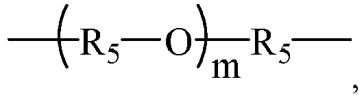
- R 3 is selected from C2-C15 linear or branched alkylene groups, C6-C17 cycloalkyl group and wherein R 5 is selected from C1-C10 linear or branched alkylene groups
- m is an integer from 1-10, e.g. 2, 3, 4, 5, 6, 7, 8, 9 and the like.
- n 1 represents a repeating unit of 4-10, e.g. 5, 6, 7, 8, 9 and the like.
- the C2-C20 may be C3, C4, C5, C6, C7, C8, C9, C10, C11, C12, C13, C14, C15, C16, C17, C18, C19 and the like.
- the C1-C10 may be C2, C3, C4, C5, C6, C7, C8, C and the like.
- the C2-C15 may be C3, C4, C5, C6, C7, C8, C9, C10, C11, C12, C13, C14 and the like.
- the C6-C17 may be C7, C8, C9, C10, C11, C12, C13, C14, C15, C16 and the like.
- a flexible epoxy resin having the specific structure is included in the main resin.
- the flexible epoxy resin provided by the present disclosure can ensure the finally obtained resin composition to have a low modulus.
- the low modulus can well alleviate the stress generated by thermal shocks, thereby avoiding cracks in solder joints or copper foil circuits caused by the mismatch between the thermal expansion coefficients of the chip and the substrate.
- the main resin comprises a phenoxy resin.
- the use of the phenoxy resin can avoid the stickiness of the finally obtained film or RCC (coated resin copper foil) caused by a too high addition amount of the flexible epoxy resin.
- the addition of a phenoxy resin to the flexible epoxy resin can avoid greatly increasing the modulus of the composition, while the low modulus of the composition is the guarantee of alleviating stress generated by thermal shocks.
- the chip, solder joint, copper foil circuit, thermally conductive insulating bonding layer, and metal substrate are all at normal positions at a normal temperature. Once subjected to thermal expansion, the metal substrate, thermally conductive insulating bonding layer and copper foil circuit will be deformed, thereby readily rendering cracks in the solder joint or copper foil circuit after thermal expansion and cooling.
- the resin composition for use in a metal substrate of the present disclosure is used as a thermally conductive insulating bonding layer, due to the low modulus thereof, only the metal substrate and the thermally conductive insulating bonding layer are deformed, but the copper foil layer is substantially not deformed when subjected to thermal expansion. Therefore, no cracking occurs in the solder joint or copper foil circuit after thermal expansion and cooling.
- the main resin is in an amount of 5-40%, e.g. 8%, 10%, 12%, 15%, 18%, 20%, 22%, 25%, 28%, 30%, 32%, 35%, 38% and the like.
- R 3 is selected from C2-C15 linear or branched alkylene groups, C6-C17 aliphatic cycloalkyl, ethyleneoxyethylene, bis(ethyleneoxy)ethylene, tris(ethyleneoxy)ethylene, propyleneoxypropylene, bis(propyleneoxy)propylene, tris(propyleneoxy)propylene, tetrakis(propyleneoxy)propylene, butyleneoxybutylene, bis(butyleneoxy)butylene, tris(butyleneoxy)butylene or tetraki s(butyleneoxy)butylene.
- the main resin further comprises a biphenyl epoxy resin.
- the biphenyl epoxy resin is added in an amount of 1-20%, e.g. 2%, 5%, 8%, 10%, 12%, 15% or 18%.
- a biphenyl epoxy resin is added into the main resin.
- the use of the biphenyl epoxy resin can increase the thermal resistance of the resin composition.
- the resin composition further comprises a curing agent.
- the curing agent is added in an amount of 1-10%, e.g. 2%, 3%, 4%, 5%, 6%, 7%, 8% or 9%.
- the curing agent is an amine curing agent.
- the curing agent is any one or a combination of at least two selected from the group consisting of ethylenediamine, diethylenetriamine, triethylenetetramine, tetraethylenepentamine, isophoronediamine, m -phenylenediamine, m -aminomethylamine, diaminodiphenyl sulfone, dicyandiamide, diaminodicyclohexyl methane, methylcyclopentanediamine, diamine methylcyclohexanediamine or diaminodiphenylmethane.
- the flexible epoxy resin is in an amount of 60-90%, e.g. 62%, 65%, 68%, 70%, 72%, 75%, 78%, 80%, 82%, 85%, 88% and the like.
- the flexible epoxy resin has a weight per epoxy equivalent of 300-500 g/eq, e.g 320 g/eq, 340 g/eq, 360 g/eq, 380 g/eq, 400 g/eq, 410 g/eq, 420 g/eq, 430 g/eq, 44 g/eq, 450 g/eq, 560 g/eq, 470 g/eq, 480 g/eq, 490 g/eq and the like.
- the phenoxy resin is in an amount of 10-40%, e.g. 12%, 15%, 18%, 20%, 22%, 25%, 28%, 30%, 32%, 35%, 38% by weight and the like.
- the content of the phenoxy resin is too low, it will not be able to prevent the film or RCC (coated resin copper foil) from being sticky. If the content of the phenoxy resin is too high, a dense protective film will be formed on the surface of the resin composition during drying process, which will hinder the evaporation of the solvent, thereby causing bubbles on the surface of the film or RCC (coated resin copper foil) so as to affect the electrical insulation of the laminate.
- the phenoxy resin has a weight average molecular weight of 30,000-65,000, e.g. 35000, 40000, 45000, 50000, 55000, 60000 and the like.
- the phenoxy resin has a too small weight average molecular weight, cracks may occur in the thermally conductive insulating bonding layer after lamination, which may affect the use of the metal base copper-clad laminate.
- the weight average molecular weight is too high, it will not be able to prevent the film or RCC (coated resin copper foil) from being sticky.
- the thermally conductive filler is in an amount of 60-95%, e.g. 62%, 65%, 68%, 70%, 72%, 75%, 78%, 80%, 82%, 85%, 88%, 90%, 92% and the like.
- the content of the thermally conductive filler affects the thermal conductivity and modulus of the resin composition. Reducing the content of the thermal conductive filler will reduce the thermal conductivity and modulus at the same time; and increasing the content of the thermal conductive filler will increase the thermal conductivity and modulus at the same time. In order to ensure a suitable thermal conductivity and a low modulus of the resin composition, the content of the thermally conductive filler is controlled to be 60 - 95%.
- the thermally conductive filler comprises any one or a combination of at least two selected from the group consisting of aluminum nitride, boron nitride, aluminum oxide, silicon carbide, zinc oxide and carbon nanotubes, further preferably any one or a combination of at least two selected from the group consisting of boron nitride, aluminum oxide and silicon carbide.
- the resin composition further comprises a curing accelerator.
- the curing accelerator is added in an amount of 0.1-2%, e.g. 0.2%, 0.5%, 0.8%, 1.0%, 1.2%, 1.5% or 1.7%.
- auxiliary agents such as antifoaming agents, dispersing agents, anti-aging agents and the like may be added without departing from the scope of the present disclosure.
- the present disclosure provides a resin varnish obtained by dissolving or dispersing the resin composition for use in a metal substrate as described in the first aspect into a solvent.
- the solvent used in the present disclosure is any one or a combination of at least two selected from the group consisting of dimethylformamide, butanone, acetone, cyclohexanone and toluene solvent.
- the present disclosure provides a film comprising the resin composition for use in a metal substrate as described in the first aspect ⁇
- the present disclosure provides a metal base copper-clad laminate comprising a metal substrate, a thermally conductive insulating bonding layer prepared from the resin composition for use in a metal substrate as described in the first aspect and a copper foil which are laminated together from bottom to top.
- the resin composition for use in a metal substrate provided by the present disclosure which is used as a thermal conductive insulating bonding layer between the metal substrate and the copper foil can well alleviate the stress of the metal substrate generated by thermal shocks, thereby avoiding cracks in solder joints or copper foil circuits caused by the mismatch between the thermal expansion coefficients of the chip and the substrate.
- the metal substrate comprises any one selected from the group consisting of an aluminum substrate, a copper substrate, an iron substrate and a steel substrate.
- the metal substrate has a thickness of 0.3-5.0 mm, e.g. 0.5 mm, 1.0 mm, 1.5 mm, 2 mm, 2.5 mm, 3 mm, 3.5 mm, 4.0 mm, 4.5 mm and the like.
- the thermally conductive insulating bonding layer has a thickness of 0.04-0.20 mm, e.g. 0.05 mm, 0.08 mm, 0.10 mm, 0.12 mm, 0.15 mm, 0.18 mm and the like.
- thermally conductive insulating bonding layer has a too small thickness, the stress generated by thermal shocks may not be well alleviated.
- the copper foil is an electrodeposited copper foil or a rolled copper foil.
- the copper foil has a thickness of 0.012-0.210 mm, e.g. 0.018 mm, 0.035 mm, 0.070 mm, 0.105 mm, 0.140 mm, 0.175 mm.
- the metal base copper-clad laminate is not limited. Exemplarily, it can be prepared by the following preparation method: dissolving or dispersing the resin composition in a solvent to obtain a resin varnish having a certain solid content, and then coating the resin varnish on a substrate film (for example, a release film), and drying to obtain a semi-cured thermally conductive insulating film, and then removing the substrate film, and then laminating together with a copper foil and a metal substrate at a high temperature to obtain a metal base copper-clad film laminate.
- a substrate film for example, a release film
- a metal base copper-clad laminate in the prior art for example, an LED lighting lamp
- the chip, solder joint, copper foil circuit, thermally conductive insulating bonding layer, and metal substrate are all at normal positions at a normal temperature. Once subjected to thermal expansion, the metal substrate, thermally conductive insulating bonding layer and copper foil circuit will be deformed, thereby readily rendering cracks in the solder joint or copper foil circuit after thermal expansion and cooling.
- the resin composition for use in a metal substrate of the present disclosure is used as a thermally conductive insulating bonding layer, due to the low modulus thereof, only the metal substrate and the thermally conductive insulating bonding layer are deformed, but the copper foil layer is substantially not deformed when subjected to thermal expansion, as shown in Fig. 4 . Therefore, no cracking occurs in the solder joint or copper foil circuit after thermal expansion and cooling.
- Resin compositions were prepared in accordance with the components shown in Tables 1-2, and metal base copper-clad laminate samples were prepared in accordance with the preparation method below.
- the components in the formula amount were uniformly mixed in a solvent, and the solid content of the varnish was controlled to be 75%.
- the varnish was applied to a copper foil having a thickness of 35 ⁇ m, and dried at 155 °C for 5 minutes to obtain a copper foil (having a thickness of 35 ⁇ m) with a semi-cured thermally conductive insulating bonding layer (having a thickness of 100 ⁇ m), which was then laminated with a surface-treated aluminum plate (having a thickness of 1.0 mm) to obtain an aluminum-based copper-clad laminate.
- Example 1 Comp.
- Example 2 Comp.
- Example 3 Comp.
- Example 4 Comp.
- Example 5 A-1 20 A-2 A-3 16 A-4 16 A-5 16 B-1 3 3 3 20 B-2 B-3 B-4 B-5 C-1 1 1 1 C-2 D-1 0.2 0.2 0.2 0.2 D-2 0.8 0.8 0.8 0.8 D-3 E-1 80 80 80 80 E-2 F-1 0.1 0.1 0.1 0.1 0.1 0.1 0.1 Table 4 Comp.
- Example 6 Comp.
- Example 7 Comp.
- Example 8 Comp.
- Example 9 Comp.
- Example 10 Comp.
- Example 11 A-1 3.2 40 10 18 11 18.5 A-2 A-3 A-4 A-5 B-1 0.6 7.5 9 1 8 0.5 B-2 B-3 B-4 B-5 C-1 0.2 2.5 1 1 1 1 C-2 D-1 0.05 0.2 0.2 0.2 0.2 0.2 D-2 0.2 0.8 0.8 0.8 0.8 D-3 E-1 96 50 80 80 80 E-2 F-1 0.1 0.1 0.1 0.1 0.1 0.1 0.1 0.1 0.1 0.1 0.1 0.1
- Example 1 Example 2
- Example 3 Example 4
- Example 5 Example 6
- Example 7 Example 8 Thermal conductivity (W/m ⁇ K) 2.0 2.0 2.0 2.0 2.0 2.0 2.0 2.0 3.0 288 °C Thermal resistance (min) 10 8 10 10 10 10 10 10 50 °C Modulus (MPa) 420 800 440 450 800 350 430 600 Number of thermal cycles (times) 1500 1300 1500 1500 1300 1500 1500 1500 Operability Excellent Excellent Excellent Excellent Excellent Good Excellent Excellent Excellent Voltage resistance (V) 5000 5000 5000 5000 5000 5000 5000 5000 5000 5000 5000 Table 6
- Example 10 Example 11
- Example 12 Example 13
- Example 14 Example 15 Thermal conductivity (W/m ⁇ K) 2.0 2.0 2.0 2.0 1.5 5.0 2.0 288 °C Thermal resistance (min) 9 9 9 10 6 6 6 50 °C Modulus (MPa) 400 600 300 800 300 1500 1500 Number of thermal cycles (times) 1500 1500 1500 1300 1500 1300 1200 Operability Excellent Excellent Excellent Excellent Excellent Excellent Excellent Excellent Excellent Excellent Voltage resistance (V) 5000
- Example 1 Comp.
- Example 2 Comp.
- Example 3 Comp.
- Example 4 Comp.
- Example 5 Thermal conductivity (W/m ⁇ K) 2.0 2.0 2.0 2.0 2.0 2.0 288 °C Thermal resistance (min) 5 5 5 5 5 50 °C Modulus (MPa) 900 850 10500 250 2100 Number of thermal cycles (times) 900 850 500 1000 800 Operability Excellent Excellent Excellent poor Excellent Voltage resistance (V) 4000 4000 5000 4000 5000 Table 8 Comp.
- Example 6 Comp.
- Example 7 Comp.
- Example 8 Comp.
- Example 9 Comp.
- Example 10 Comp.
- Example 11 Thermal conductivity (W/m ⁇ K) 7.0 0.8 2.0 2.0 2.0 2.0 288 °C thermal resistance (min) 2 5 8 8 8 8 50 °C Modulus (MPa) 3000 200 1000 280 900 270 Number of thermal cycles (times) 800 1300 900 1300 900 1300 Operability Excellent Good Excellent Poor Excellent Poor Voltage resistance (V) 2000 5000 5000 5000 5000 5000 5000
- the metal base laminates prepared by the disclosure have better comprehensive performance, wherein the 288 °C thermal resistance is 6 min or more; the number of thermal cycles is 1200 or more; and the operability is excellent. All laminates can satisfy the application requirements.
- Example 1 when the weight average molecular weight of the phenoxy resin is not within the range of 30,000 to 65,000, for example, when the weight average molecular weight of the phenoxy resin of Example 5 is less than 30,000, the laminate sample has a number of thermal cycles of 1300; and for another example, when the weight average molecular weight of the phenoxy resin of Example 6 is higher than 65,000, there are some certain influence on operability.
- Example 1 and Examples 9-11 when no biphenyl epoxy resin is added, the laminate sample has a poor 288 °C thermal resistance, which is 9 min.
- the laminate sample when the main resin accounts for 40% of the total weight of the resin composition, the laminate sample has a low modulus at 50 °C, but has a thermal conductivity of 1.5 W/m ⁇ K, and a 288 °C thermal resistance of 6 min. While when the thermally conductive filler accounts for 95% of the total weight of the resin composition, the thermal conductivity of the laminate sample is significantly increased; but the modulus at 50 °C achieves 1500 MPa; and the 288 °C thermal resistance is 6 min. As can be seen from the comparison between Example 1 and Example 15, the use of the active ester curing agent greatly increases the modulus of the laminate sample; and its 288 °C thermal resistance is 6 min, and the voltage resistance value is as low as 4000 V.
- Example 1 As can be seen from the comparison between Example 1 and Comparative Examples 1-3, although the laminate samples in Comparative Examples 1-2 can also obtain a low modulus, but they have a poor 288 °C thermal resistance and poor thermal cycle property, which is because the flexible epoxy used in Comparative Examples 1-2 contains a hydroxyl structure. Since Comparative Example 3 used an ordinary bisphenol-A epoxy resin, its modulus at 50 °C is as high as 10,500 MPa, and its 288 °C thermal resistance and thermal cycle property are also poor. As can be seen from the comparison between Example 1 and Comparative Example 4, when only a flexible epoxy resin is used in the main resin, the resulting laminate sample has a poor thermal resistance and operability.
- Example 1 and Comparative Example 5 when only a phenoxy resin is used in the main resin, the resulting laminate sample has a poor 288 °C thermal resistance and poor thermal cycle property, and has a modulus up to 2,100 MPa.
- Example 1 and Comparative Examples 6 and 7 when the addition amount of the main resin is not within the range of 5 to 40%, for example when the addition amount is too small, the laminate has a high modulus and a poor thermal resistance and thermal cycle property; when the addition amount is too high, the thermal conductivity is reduced, the thermal resistance is poor, and the operability is affected to some extent.
- Example 1 and Comparative Examples 8 and 11 when the amount of the flexible oxygen resin added to the main resin is too small, and the amount of the phenoxy resin added to the main resin is too high, the laminate has a high modulus, a slightly poor thermal resistance and poor thermal cycle property; when the amount of the flexible oxygen resin added to the main resin is too high, and the amount of the phenoxy resin added to the main resin is too small, the laminate has a poor thermal resistance and poor operability.
- Example 1 when the amount of the phenoxy resin added to the main resin is too small, the laminate has a poor thermal resistance and poor operability; when the amount of the flexible epoxy resin to the main resin is too small, the laminate has high modulus, and poor thermal resistance and thermal cycle property.
- Example 16 The difference from Example 1 was that the resin composition provided in Example 1 was kept unchanged, but the thickness of the thermally conductive insulating bonding layer was changed.
- the thicknesses of the thermally conductive insulating bonding layers in resulting aluminum-based copper-clad laminates were 40 ⁇ m (Example 16), 200 ⁇ m (Example 17), 30 ⁇ m (Example 18) and 220 ⁇ m (Example 19).
- Example 16-19 The metal base copper-clad laminates provided in Examples 16-19 were tested for performance by referring to Performance Test 1. The test results are shown in Table 9. Table 9 Example 16 Example 17 Example 18 Example 19 Thermal impedance (°C ⁇ cm 2 /W) 0.2 1.0 0.15 1.1 288 °C Thermal resistance (min) 10 10 10 10 50 °C Modulus (MPa) 420 420 420 420 Number of thermal cycles (times) 1200 1500 1000 1500 Operability Excellent Excellent Excellent Excellent Excellent Excellent Voltage resistance (V) 3000 8000 2000 8000
- the preferable thickness of the thermally conductive insulating bonding layer of the present disclosure is 0.04-0.20 mm.
- the metal base copper-clad laminate having such thickness prepared by the present disclosure has better comprehensive performance. If the thermally conductive insulating bonding layer has a too small thickness, the stress generated by thermal shocks cannot be sufficiently alleviated, and the voltage resistance is low. If the thermally conductive insulating bonding layer has a too high thickness, although the stress generated by thermal shocks can be sufficiently alleviated, the thermal impedance becomes high, which is not conducive to the rapid heat dissipation of the metal substrate.
Landscapes
- Chemical & Material Sciences (AREA)
- Organic Chemistry (AREA)
- Health & Medical Sciences (AREA)
- Chemical Kinetics & Catalysis (AREA)
- Medicinal Chemistry (AREA)
- Polymers & Plastics (AREA)
- Materials Engineering (AREA)
- Engineering & Computer Science (AREA)
- Life Sciences & Earth Sciences (AREA)
- Wood Science & Technology (AREA)
- Inorganic Chemistry (AREA)
- Physics & Mathematics (AREA)
- Fluid Mechanics (AREA)
- Laminated Bodies (AREA)
- Adhesive Tapes (AREA)
- Epoxy Resins (AREA)
- Adhesives Or Adhesive Processes (AREA)
- Compositions Of Macromolecular Compounds (AREA)
Description
- The present disclosure belongs to the field of laminates, and relates to a resin composition for a metal substrate, and a resin varnish and a metal base copper-clad laminate comprising the same.
- Along with the mass production and light, thin, small and multi-function designs of electronic information products, printed circuit boards which are served as the main support of electronic components are also being continuously improved to provide high-density wiring, thin, fine pores, and high heat dissipation. In this context, metal base copper-clad laminates with high heat dissipation were developed. In a case where a metal base copper-clad laminate is applied to a high-power LED lamp, the thermal expansion coefficient of the high-power chip is much less than that of the metal substrate which results in great difference between stress released by the chip and the substrate after thermal shocks such that cracks are occurred in weakest solder joints or copper foil circuits, thereby affecting reliability. The metal base copper-clad laminate is generally made by bonding a metal substrate, a thermally conductive insulating bonding layer and a copper foil. The presence of a thermally conductive insulating bonding layer may alleviate the stress generated by thermal shocks to some extent, but still cannot satisfy the reliability requirements.
CN104708869A discloses a high thermal-conductive aluminum-based copper-clad laminate and a method for preparing the same, comprising a copper foil layer, a high thermal conductive insulating layer and an aluminum plate arranged in sequence from the inside to the outside, wherein the high thermal conductive insulating layer is filled with alumina fibers made by micro-arc oxidation. The patent discloses improving the heat dissipation capability of the aluminum-based copper-clad board and increasing the reliability of the aluminum-based copper-clad board, but it does not involve how to solve the problem of weld point or copper foil destruction from the stress generated by the thermal shock.CN103468188A discloses a magnetic composite glue comprising 1 to 200 parts by weight of permeability magnetic conductive powder, 10 parts by weight of a resin, 1 part by weight of calcium carbonate, 0.1 to 1 part by weight of an active dispersant and other additives, and 0.1-1 part by weight of a latent curing accelerator, or comprising 1000-2000 parts by weight of permeability magnetic conductive powder, 10 parts by weight of rubber, 1 part by weight of calcium carbonate, 1-5 parts by weight of an active dispersant and other additives, and 1-5 parts by weight of a latent curing accelerator. After curing, the glue of this patent generates very little stress on the object in contact with it when subjected to thermal shock cycles from -40 °C and 125 °C such that sheet material with a strength of 1.5 N will not crack. The curing strength is such that it can withstand a destructive force of 50 N or more after subjected to 200 thermal shock cycles from -40 °C to 85 °C. However, it remains to be studied whether it can be applied to the field of laminates.CN104610707A discloses a metal-base copper clad laminate for high-power LEDs manufactured through high-performance RCC (resin coated copper foil). The metal-base copper clad laminate comprises an epoxy resin composition, wherein the solid components of the epoxy resin composition are comprised, in parts by mass, as follows: (A) 5-35 parts of bisphenol A type epoxy resin, 0-10 parts of phenoxy resin and 5-30 parts of dicyclopentadiene phenol epoxy resin; (B) 5-35 parts of nitrile rubber; (C) 50-80 parts of filler; (D) 1-10 parts of an amine curing agent; (E) 0.1-2 parts of an accelerator. - In order to improve the toughness and flexibility of the film material, a small amount of thermoplastic resin, rubber-toughening epoxy resin or other epoxy resin for modifying toughness may be added to the main resin. Due to low thermal conductivity and poor resistance against thermal shocks, the resin composition cannot be used as a thermal conductive insulating bonding layer in metal base copper-clad laminates.
- Therefore, there is a need to develop a thermally conductive resin composition which has excellent resistance against thermal shocks for using in a metal substrate.
- An object of the present disclosure is to provide a resin composition for use in a metal substrate, and a resin varnish and a metal base copper-clad laminate comprising the same. The resin composition provided by the present disclosure can withstand changes in thermal shocks, and has a low modulus such that cracking of solder joints or copper foil circuits caused by the mismatch between the thermal expansion coefficients of the chip and the substrate can be avoided.
- To achieve the object, the present disclosure discloses the following technical solutions.
- In a first aspect, the present disclosure provides a resin composition for use in a metal substrate, comprising 5-40% of a main resin and 60-95% of a thermally conductive filler when the total weight of the resin composition is calculated as 100%.
- Wherein, the main resin comprises 60-90% of a flexible epoxy resin and 10-40% of a phenoxy resin when the total weight of the main resin is calculated as 100%.
- Wherein, the flexible epoxy resin has a structure as shown in Formula I:

- Wherein R is selected from C2-C20 linear or branched alkylene groups, -CO-R1-CO- or -R2-O-R3-O-R4-.
- Wherein R1 is selected from C2-C20 linear or branched alkylene groups; R2 and R4 are each independently selected from C1-C10 linear or branched alkylene groups; R3 is selected from C2-C15 linear or branched alkylene groups, C6-C17 cycloalkyl group and
- n1 represents a repeating unit of 4-10, e.g. 5, 6, 7, 8, 9 and the like.
- The C2-C20 may be C3, C4, C5, C6, C7, C8, C9, C10, C11, C12, C13, C14, C15, C16, C17, C18, C19 and the like.
- The C1-C10 may be C2, C3, C4, C5, C6, C7, C8, C and the like.
- The C2-C15 may be C3, C4, C5, C6, C7, C8, C9, C10, C11, C12, C13, C14 and the like.
- The C6-C17 may be C7, C8, C9, C10, C11, C12, C13, C14, C15, C16 and the like.
- In the present disclosure, a flexible epoxy resin having the specific structure is included in the main resin. The flexible epoxy resin provided by the present disclosure can ensure the finally obtained resin composition to have a low modulus. The low modulus can well alleviate the stress generated by thermal shocks, thereby avoiding cracks in solder joints or copper foil circuits caused by the mismatch between the thermal expansion coefficients of the chip and the substrate.
- Meanwhile, the main resin comprises a phenoxy resin. The use of the phenoxy resin can avoid the stickiness of the finally obtained film or RCC (coated resin copper foil) caused by a too high addition amount of the flexible epoxy resin. Moreover, different from other epoxy resins, the addition of a phenoxy resin to the flexible epoxy resin can avoid greatly increasing the modulus of the composition, while the low modulus of the composition is the guarantee of alleviating stress generated by thermal shocks.
- In a case where a metal base copper-clad laminate in the prior art is used (for example, an LED lighting lamp), the chip, solder joint, copper foil circuit, thermally conductive insulating bonding layer, and metal substrate are all at normal positions at a normal temperature. Once subjected to thermal expansion, the metal substrate, thermally conductive insulating bonding layer and copper foil circuit will be deformed, thereby readily rendering cracks in the solder joint or copper foil circuit after thermal expansion and cooling. However, in a case where the resin composition for use in a metal substrate of the present disclosure is used as a thermally conductive insulating bonding layer, due to the low modulus thereof, only the metal substrate and the thermally conductive insulating bonding layer are deformed, but the copper foil layer is substantially not deformed when subjected to thermal expansion. Therefore, no cracking occurs in the solder joint or copper foil circuit after thermal expansion and cooling.
- The main resin is in an amount of 5-40%, e.g.8%, 10%, 12%, 15%, 18%, 20%, 22%, 25%, 28%, 30%, 32%, 35%, 38% and the like.
- In the present disclosure, R3 is selected from C2-C15 linear or branched alkylene groups, C6-C17 aliphatic cycloalkyl, ethyleneoxyethylene, bis(ethyleneoxy)ethylene, tris(ethyleneoxy)ethylene, propyleneoxypropylene, bis(propyleneoxy)propylene, tris(propyleneoxy)propylene, tetrakis(propyleneoxy)propylene, butyleneoxybutylene, bis(butyleneoxy)butylene, tris(butyleneoxy)butylene or tetraki s(butyleneoxy)butylene.
- Preferably, the main resin further comprises a biphenyl epoxy resin.
- Preferably, when the total weight of the main resin is calculated as 100%, the biphenyl epoxy resin is added in an amount of 1-20%, e.g. 2%, 5%, 8%, 10%, 12%, 15% or 18%.
- A biphenyl epoxy resin is added into the main resin. The use of the biphenyl epoxy resin can increase the thermal resistance of the resin composition.
- Preferably, the resin composition further comprises a curing agent.
- Preferably, when the total weight of the main resin is calculated as 100%, the curing agent is added in an amount of 1-10%, e.g. 2%, 3%, 4%, 5%, 6%, 7%, 8% or 9%.
- Preferably, the curing agent is an amine curing agent.
- Preferably, the curing agent is any one or a combination of at least two selected from the group consisting of ethylenediamine, diethylenetriamine, triethylenetetramine, tetraethylenepentamine, isophoronediamine, m-phenylenediamine, m-aminomethylamine, diaminodiphenyl sulfone, dicyandiamide, diaminodicyclohexyl methane, methylcyclopentanediamine, diamine methylcyclohexanediamine or diaminodiphenylmethane.
- The flexible epoxy resin is in an amount of 60-90%, e.g. 62%, 65%, 68%, 70%, 72%, 75%, 78%, 80%, 82%, 85%, 88% and the like.
- Preferably, the flexible epoxy resin has a weight per epoxy equivalent of 300-500 g/eq, e.g 320 g/eq, 340 g/eq, 360 g/eq, 380 g/eq, 400 g/eq, 410 g/eq, 420 g/eq, 430 g/eq, 44 g/eq, 450 g/eq, 560 g/eq, 470 g/eq, 480 g/eq, 490 g/eq and the like.
- The phenoxy resin is in an amount of 10-40%, e.g. 12%, 15%, 18%, 20%, 22%, 25%, 28%, 30%, 32%, 35%, 38% by weight and the like.
- If the content of the phenoxy resin is too low, it will not be able to prevent the film or RCC (coated resin copper foil) from being sticky. If the content of the phenoxy resin is too high, a dense protective film will be formed on the surface of the resin composition during drying process, which will hinder the evaporation of the solvent, thereby causing bubbles on the surface of the film or RCC (coated resin copper foil) so as to affect the electrical insulation of the laminate.
- Preferably, the phenoxy resin has a weight average molecular weight of 30,000-65,000, e.g. 35000, 40000, 45000, 50000, 55000, 60000 and the like.
- When the phenoxy resin has a too small weight average molecular weight, cracks may occur in the thermally conductive insulating bonding layer after lamination, which may affect the use of the metal base copper-clad laminate. When the weight average molecular weight is too high, it will not be able to prevent the film or RCC (coated resin copper foil) from being sticky.
- The thermally conductive filler is in an amount of 60-95%, e.g. 62%, 65%, 68%, 70%, 72%, 75%, 78%, 80%, 82%, 85%, 88%, 90%, 92% and the like.
- The content of the thermally conductive filler affects the thermal conductivity and modulus of the resin composition. Reducing the content of the thermal conductive filler will reduce the thermal conductivity and modulus at the same time; and increasing the content of the thermal conductive filler will increase the thermal conductivity and modulus at the same time. In order to ensure a suitable thermal conductivity and a low modulus of the resin composition, the content of the thermally conductive filler is controlled to be 60 - 95%.
- Preferably, the thermally conductive filler comprises any one or a combination of at least two selected from the group consisting of aluminum nitride, boron nitride, aluminum oxide, silicon carbide, zinc oxide and carbon nanotubes, further preferably any one or a combination of at least two selected from the group consisting of boron nitride, aluminum oxide and silicon carbide.
- Preferably, the resin composition further comprises a curing accelerator.
- Preferably, when the total weight of the main resin is calculated as 100%, the curing accelerator is added in an amount of 0.1-2%, e.g. 0.2%, 0.5%, 0.8%, 1.0%, 1.2%, 1.5% or 1.7%.
- In the formulation of the present disclosure, in addition to the above components, some auxiliary agents such as antifoaming agents, dispersing agents, anti-aging agents and the like may be added without departing from the scope of the present disclosure.
- In a second aspect, the present disclosure provides a resin varnish obtained by dissolving or dispersing the resin composition for use in a metal substrate as described in the first aspect into a solvent.
- The solvent used in the present disclosure is any one or a combination of at least two selected from the group consisting of dimethylformamide, butanone, acetone, cyclohexanone and toluene solvent.
- In a third aspect, the present disclosure provides a film comprising the resin composition for use in a metal substrate as described in the first aspect∘
- In a fourth aspect, the present disclosure provides a metal base copper-clad laminate comprising a metal substrate, a thermally conductive insulating bonding layer prepared from the resin composition for use in a metal substrate as described in the first aspect and a copper foil which are laminated together from bottom to top.
- The resin composition for use in a metal substrate provided by the present disclosure which is used as a thermal conductive insulating bonding layer between the metal substrate and the copper foil can well alleviate the stress of the metal substrate generated by thermal shocks, thereby avoiding cracks in solder joints or copper foil circuits caused by the mismatch between the thermal expansion coefficients of the chip and the substrate.
- Preferably, the metal substrate comprises any one selected from the group consisting of an aluminum substrate, a copper substrate, an iron substrate and a steel substrate.
- Preferably, the metal substrate has a thickness of 0.3-5.0 mm, e.g. 0.5 mm, 1.0 mm, 1.5 mm, 2 mm, 2.5 mm, 3 mm, 3.5 mm, 4.0 mm, 4.5 mm and the like.
- Preferably, the thermally conductive insulating bonding layer has a thickness of 0.04-0.20 mm, e.g. 0.05 mm, 0.08 mm, 0.10 mm, 0.12 mm, 0.15 mm, 0.18 mm and the like.
- If the thermally conductive insulating bonding layer has a too small thickness, the stress generated by thermal shocks may not be well alleviated.
- Preferably, the copper foil is an electrodeposited copper foil or a rolled copper foil.
- Preferably, the copper foil has a thickness of 0.012-0.210 mm, e.g. 0.018 mm, 0.035 mm, 0.070 mm, 0.105 mm, 0.140 mm, 0.175 mm.
- In the present disclosure, the metal base copper-clad laminate is not limited. Exemplarily, it can be prepared by the following preparation method: dissolving or dispersing the resin composition in a solvent to obtain a resin varnish having a certain solid content, and then coating the resin varnish on a substrate film (for example, a release film), and drying to obtain a semi-cured thermally conductive insulating film, and then removing the substrate film, and then laminating together with a copper foil and a metal substrate at a high temperature to obtain a metal base copper-clad film laminate.
- It may also be prepared by the following preparation method: coating a resin varnish having a certain solid content onto a copper foil, and drying to obtain a copper foil with a semi-cured thermally conductive insulating bonding layer, and then laminating the same with a metal substrate to obtain a metal base copper-clad laminate.
- Compared with the prior art, the present disclosure has the following beneficial effects:
- (1) In the present disclosure, a flexible epoxy resin is included in the main resin. The flexible epoxy resin provided by the present disclosure can ensure the finally obtained resin composition to have a low modulus. The low modulus can well alleviate the stress generated by thermal shocks, thereby avoiding cracks in solder joints or copper foil circuits caused by the mismatch between the thermal expansion coefficients of the chip and the substrate.
- (2) The main resin comprises a phenoxy resin. The use of the phenoxy resin can avoid the stickiness of the finally obtained film or RCC (coated resin copper foil) caused by a too high addition amount of the flexible epoxy resin. Moreover, different from other epoxy resins, the addition of a phenoxy resin to the flexible epoxy resin can avoid greatly increasing the modulus of the composition, while the low modulus of the composition is the guarantee of alleviating stress generated by thermal shocks.
- (3) The resin composition for use in a metal substrate provided by the present disclosure has a low modulus, which is less than 1500 MPa and may be as low as 300 MPa. The metal base copper-clad laminate prepared by using the resin composition has a good thermal resistance, a good resistance against thermal shocks and high operability, wherein it has a 288 °C thermal resistance of 6 min or more, up to 10 min; and has a resistance against 1000 or more, up to 1500 or more thermal cycles.
-
-
Fig. 1 is a schematic cross-sectional view showing a metal base copper-clad laminate and a chip at a normal temperature. -
Fig. 2 is a schematic cross-sectional view showing a metal base copper-clad laminate and a chip in the prior art in a state of thermal expansion. -
Fig.3 is a schematic cross-sectional view showing cracking of solder joints of a metal base copper-clad laminate and a chip in the prior art after thermal expansion and cooling. -
Fig. 4 is a schematic cross-sectional view showing a metal base copper-clad laminate and a chip in the present disclosure in a state of thermal expansion. - Wherein, 1 - chip; 2 - solder joint; 3 - copper foil circuit; 4 - thermally conductive insulating bonding layer; 5 - metal substrate.
- The technical solution of the present disclosure will be further described below by way of specific embodiments. It should be understood by those skilled in the art that the examples are only to help understanding the present disclosure, and shall not be construed as limiting the disclosure.
- It can be seen from
Figs. 1-3 that in a case where a metal base copper-clad laminate in the prior art is used (for example, an LED lighting lamp), the chip, solder joint, copper foil circuit, thermally conductive insulating bonding layer, and metal substrate are all at normal positions at a normal temperature. Once subjected to thermal expansion, the metal substrate, thermally conductive insulating bonding layer and copper foil circuit will be deformed, thereby readily rendering cracks in the solder joint or copper foil circuit after thermal expansion and cooling. However, in a case where the resin composition for use in a metal substrate of the present disclosure is used as a thermally conductive insulating bonding layer, due to the low modulus thereof, only the metal substrate and the thermally conductive insulating bonding layer are deformed, but the copper foil layer is substantially not deformed when subjected to thermal expansion, as shown inFig. 4 . Therefore, no cracking occurs in the solder joint or copper foil circuit after thermal expansion and cooling. - The materials referred to in the following Examples and Comparative Examples, and brand information thereof are as follows:
- (A) Flexible epoxy resin
- A-1: Product model EXA-4850-150, weight per epoxy equivalent 450 g/eq, manufactured by Dainippon Ink and Chemicals Inc.;
- A-2: Product model EXA-4850-1000, weight per epoxy equivalent 350 g/eq, manufactured by Dainippon Ink and Chemicals Inc.;
- A-3: Product model EXA-4816, weight per epoxy equivalent 403 g/eq, manufactured by Dainippon Ink and Chemicals Inc., having the structure as follows:

- A-4: Product model DX7160, weight per epoxy equivalent 430 g/eq, manufactured by Jiashengde Material Technology Inc., Hunan, China, having the structure as follows:

- A-5: An ordinary bisphenol-A epoxy resin, product model NPES-901, weight per epoxy equivalent 475g/eq, manufactured by Nanya Electronic Materials Inc.;
- (B) Phenoxy resin
- B-1: Product model EPONOL Resin53-BH-35, weight average molecular weight 55,000, manufactured by Momenti ye;
- B-2: Product model PKHH, weight average molecular weight 50,000, manufactured by Inchem;
- B-3: Product model ERF-001, weight average molecular weight 40,000, manufactured by Nippon Steel Chemical;
- B-4: Product model YP-50SB, weight average molecular weight 25,000, manufactured by Tohto Kasei;
- B-5: Product model YP-50, weight average molecular weight 70,000, manufactured by Tohto Kasei;
- (C) Biphenyl epoxy resin
- C-1: Product model NC-3000H, weight per epoxy equivalent 285 g/eq, manufactured by Nippon Kayaku Inc.;
- C-2: Product model YX-4000, weight per epoxy equivalent 185 g/eq, manufactured by Mitsubishi Chemical Inc.;
- (D) Curing agent
- D-1: Triethylenetetramine;
- D-2: Diaminodiphenyl sulfone;
- D-3: An active ester, product model HPC-8000-651, manufactured by Dainippon Ink and Chemicals Inc.;
- (E) Thermally conductive filler
- E-1: Alumina, Sumitomo, Japan;
- E-2: Boron nitride, Momentive, American;
- (F) Curing accelerator
F-1: 2-Methylimidazole - Resin compositions were prepared in accordance with the components shown in Tables 1-2, and metal base copper-clad laminate samples were prepared in accordance with the preparation method below.
- The components in the formula amount were uniformly mixed in a solvent, and the solid content of the varnish was controlled to be 75%. The varnish was applied to a copper foil having a thickness of 35 µm, and dried at 155 °C for 5 minutes to obtain a copper foil (having a thickness of 35 µm) with a semi-cured thermally conductive insulating bonding layer (having a thickness of 100 µm), which was then laminated with a surface-treated aluminum plate (having a thickness of 1.0 mm) to obtain an aluminum-based copper-clad laminate.
- Resin compositions were prepared in accordance with the components shown in Tables 3 and 4, and metal base copper-clad laminate samples were prepared in accordance with the preparation method described in the examples.
Table 1 Example 1 Example 2 Example 3 Example 4 Example 5 Example 6 Example 7 Example 8 A-1 16 16 16 16 16 16 16 A-2 16 A-3 A-4 A-5 B-1 3 3 3 3 B-2 3 B-3 3 B-4 3 B-5 3 C-1 1 1 1 1 1 1 1 C-2 1 D-1 0.2 0.2 0.2 0.2 0.2 0.2 0.2 1 D-2 0.8 0.8 0.8 0.8 0.8 0.8 0.8 D-3 E-1 80 80 80 80 80 80 80 60 E-2 20 F-1 0.1 0.1 0.1 0.1 0.1 0.1 0.1 0.1 Table 2 Example 9 Example 10 Example 11 Example 12 Example 13 Example 14 Example 15 A-1 16.8 12 18 12 32 4 16 A-2 A-3 A-4 A-5 B-1 3.2 8 2 4 4 0.5 3 B-2 B-3 B-4 B-5 C-1 4 1 C-2 4 0.5 D-1 0.2 0.2 0.2 0.2 0.4 0.2 D-2 0.8 0.8 0.8 0.8 1.6 0.8 D-3 1 E-1 80 80 80 80 60 95 80 E-2 F-1 0.1 0.1 0.1 0.1 0.1 0.1 0.1 Table 3 Comp. Example 1 Comp. Example 2 Comp. Example 3 Comp. Example 4 Comp. Example 5 A-1 20 A-2 A-3 16 A-4 16 A-5 16 B-1 3 3 3 20 B-2 B-3 B-4 B-5 C-1 1 1 1 C-2 D-1 0.2 0.2 0.2 0.2 0.2 D-2 0.8 0.8 0.8 0.8 0.8 D-3 E-1 80 80 80 80 80 E-2 F-1 0.1 0.1 0.1 0.1 0.1 Table 4 Comp. Example 6 Comp. Example 7 Comp. Example 8 Comp. Example 9 Comp. Example 10 Comp. Example 11 A-1 3.2 40 10 18 11 18.5 A-2 A-3 A-4 A-5 B-1 0.6 7.5 9 1 8 0.5 B-2 B-3 B-4 B-5 C-1 0.2 2.5 1 1 1 1 C-2 D-1 0.05 0.2 0.2 0.2 0.2 0.2 D-2 0.2 0.8 0.8 0.8 0.8 0.8 D-3 E-1 96 50 80 80 80 80 E-2 F-1 0.1 0.1 0.1 0.1 0.1 0.1 - The metal base copper-clad laminates provided in Examples 1-15 and Comparative Examples 1-11 were tested for performance as follows:
- (1) Thermal conductivity/thermal impedance: The metal substrates were made into samples of 25.4 mm × 25.4 mm to test the thermal conductivity/thermal impedance of the laminates by referring to the ASTM D5470 test method;
- (2) Thermal resistance (288 °C): The thermal resistance of the laminates was tested by referring to the experimental conditions in the IPC-TM-650 2.4.13 method;
- (3) Modulus: The modulus of the insulating bonding layers was tested by referring to the experimental conditions in the IPC-TM-650 2.4.24.4 method;
- (4) Number of thermal cycles: After several thermal cycles between -50 °C and 150 °C, the laminates were sliced and analyzed for the binding of each layer to determine whether delamination occurred;
- (5) Operationality: The evaluation was carried out based on convenience in actual use: no stickiness was evaluated as "excellent", a little stickiness was evaluated as "good", and stickiness was evaluated as "poor";
- (6) Voltage resistance test: The voltage resistance of the thermally conductive insulating layers was tested according to the method in T/CPCA 4105-2016. The average value of 5 points was calculated;
- (7) Weight average molecular weight: Performed using the test method specified in
GB/T 21863-2008 - The test results are shown in Table 5-8.
Table 5 Example 1 Example 2 Example 3 Example 4 Example 5 Example 6 Example 7 Example 8 Thermal conductivity (W/m·K) 2.0 2.0 2.0 2.0 2.0 2.0 2.0 3.0 288 °C Thermal resistance (min) 10 8 10 10 10 10 10 10 50 °C Modulus (MPa) 420 800 440 450 800 350 430 600 Number of thermal cycles (times) 1500 1300 1500 1500 1300 1500 1500 1500 Operability Excellent Excellent Excellent Excellent Excellent Good Excellent Excellent Voltage resistance (V) 5000 5000 5000 5000 5000 5000 5000 5000 Table 6 Example 9 Example 10 Example 11 Example 12 Example 13 Example 14 Example 15 Thermal conductivity (W/m·K) 2.0 2.0 2.0 2.0 1.5 5.0 2.0 288 °C Thermal resistance (min) 9 9 9 10 6 6 6 50 °C Modulus (MPa) 400 600 300 800 300 1500 1500 Number of thermal cycles (times) 1500 1500 1500 1300 1500 1300 1200 Operability Excellent Excellent Excellent Excellent Excellent Excellent Excellent Voltage resistance (V) 5000 5000 5000 5000 5000 3500 4000 Table 7 Comp. Example 1 Comp. Example 2 Comp. Example 3 Comp. Example 4 Comp. Example 5 Thermal conductivity (W/m·K) 2.0 2.0 2.0 2.0 2.0 288 °C Thermal resistance (min) 5 5 5 5 5 50 °C Modulus (MPa) 900 850 10500 250 2100 Number of thermal cycles (times) 900 850 500 1000 800 Operability Excellent Excellent Excellent poor Excellent Voltage resistance (V) 4000 4000 5000 4000 5000 Table 8 Comp. Example 6 Comp. Example 7 Comp. Example 8 Comp. Example 9 Comp. Example 10 Comp. Example 11 Thermal conductivity (W/m·K) 7.0 0.8 2.0 2.0 2.0 2.0 288 °C thermal resistance (min) 2 5 8 8 8 8 50 °C Modulus (MPa) 3000 200 1000 280 900 270 Number of thermal cycles (times) 800 1300 900 1300 900 1300 Operability Excellent Good Excellent Poor Excellent Poor Voltage resistance (V) 2000 5000 5000 5000 5000 5000 - It can be seen from the Examples and the Performance Test that the metal base laminates prepared by the disclosure have better comprehensive performance, wherein the 288 °C thermal resistance is 6 min or more; the number of thermal cycles is 1200 or more; and the operability is excellent. All laminates can satisfy the application requirements.
- As can be seen from the comparison between Example 1 and Examples 3-6, when the weight average molecular weight of the phenoxy resin is not within the range of 30,000 to 65,000, for example, when the weight average molecular weight of the phenoxy resin of Example 5 is less than 30,000, the laminate sample has a number of thermal cycles of 1300; and for another example, when the weight average molecular weight of the phenoxy resin of Example 6 is higher than 65,000, there are some certain influence on operability. As can be seen from the comparison between Example 1 and Examples 9-11, when no biphenyl epoxy resin is added, the laminate sample has a poor 288 °C thermal resistance, which is 9 min. As can be seen from the comparison between Example 1 and Examples 13-14, when the main resin accounts for 40% of the total weight of the resin composition, the laminate sample has a low modulus at 50 °C, but has a thermal conductivity of 1.5 W/m·K, and a 288 °C thermal resistance of 6 min. While when the thermally conductive filler accounts for 95% of the total weight of the resin composition, the thermal conductivity of the laminate sample is significantly increased; but the modulus at 50 °C achieves 1500 MPa; and the 288 °C thermal resistance is 6 min. As can be seen from the comparison between Example 1 and Example 15, the use of the active ester curing agent greatly increases the modulus of the laminate sample; and its 288 °C thermal resistance is 6 min, and the voltage resistance value is as low as 4000 V.
- As can be seen from the comparison between Example 1 and Comparative Examples 1-3, although the laminate samples in Comparative Examples 1-2 can also obtain a low modulus, but they have a poor 288 °C thermal resistance and poor thermal cycle property, which is because the flexible epoxy used in Comparative Examples 1-2 contains a hydroxyl structure. Since Comparative Example 3 used an ordinary bisphenol-A epoxy resin, its modulus at 50 °C is as high as 10,500 MPa, and its 288 °C thermal resistance and thermal cycle property are also poor. As can be seen from the comparison between Example 1 and Comparative Example 4, when only a flexible epoxy resin is used in the main resin, the resulting laminate sample has a poor thermal resistance and operability. As can be seen from the comparison between Example 1 and Comparative Example 5, when only a phenoxy resin is used in the main resin, the resulting laminate sample has a poor 288 °C thermal resistance and poor thermal cycle property, and has a modulus up to 2,100 MPa. As can be seen from the comparison between Example 1 and Comparative Examples 6 and 7, when the addition amount of the main resin is not within the range of 5 to 40%, for example when the addition amount is too small, the laminate has a high modulus and a poor thermal resistance and thermal cycle property; when the addition amount is too high, the thermal conductivity is reduced, the thermal resistance is poor, and the operability is affected to some extent. As can be seen from the comparison between Example 1 and Comparative Examples 8 and 11, when the amount of the flexible oxygen resin added to the main resin is too small, and the amount of the phenoxy resin added to the main resin is too high, the laminate has a high modulus, a slightly poor thermal resistance and poor thermal cycle property; when the amount of the flexible oxygen resin added to the main resin is too high, and the amount of the phenoxy resin added to the main resin is too small, the laminate has a poor thermal resistance and poor operability. As can be seen from the comparison between Example 1 and Comparative Examples 9-10, when the amount of the phenoxy resin added to the main resin is too small, the laminate has a poor thermal resistance and poor operability; when the amount of the flexible epoxy resin to the main resin is too small, the laminate has high modulus, and poor thermal resistance and thermal cycle property.
- The difference from Example 1 was that the resin composition provided in Example 1 was kept unchanged, but the thickness of the thermally conductive insulating bonding layer was changed. The thicknesses of the thermally conductive insulating bonding layers in resulting aluminum-based copper-clad laminates were 40 µm (Example 16), 200 µm (Example 17), 30 µm (Example 18) and 220 µm (Example 19).
- The metal base copper-clad laminates provided in Examples 16-19 were tested for performance by referring to
Performance Test 1. The test results are shown in Table 9.Table 9 Example 16 Example 17 Example 18 Example 19 Thermal impedance (°C·cm2/W) 0.2 1.0 0.15 1.1 288 °C Thermal resistance (min) 10 10 10 10 50 °C Modulus (MPa) 420 420 420 420 Number of thermal cycles (times) 1200 1500 1000 1500 Operability Excellent Excellent Excellent Excellent Voltage resistance (V) 3000 8000 2000 8000 - As can be seen from the comparison between Example 1, Examples 16-17 and Examples 18-19, the preferable thickness of the thermally conductive insulating bonding layer of the present disclosure is 0.04-0.20 mm. The metal base copper-clad laminate having such thickness prepared by the present disclosure has better comprehensive performance. If the thermally conductive insulating bonding layer has a too small thickness, the stress generated by thermal shocks cannot be sufficiently alleviated, and the voltage resistance is low. If the thermally conductive insulating bonding layer has a too high thickness, although the stress generated by thermal shocks can be sufficiently alleviated, the thermal impedance becomes high, which is not conducive to the rapid heat dissipation of the metal substrate.
Claims (10)
- A resin composition for a metal substrate comprising 5-40% of a main resin and 60-95% of a thermally conductive filler when the total weight of the resin composition is calculated as 100%;wherein the main resin comprises 60-90% of a flexible epoxy resin having a structure as shown in Formula I and 10-40% of a phenoxy resin when the total weight of the main resin is calculated as 100%,
 wherein R is selected from C2-C20 linear or branched alkylene groups, -CO-R1-CO- or -R2-O-R3-O-R4-,wherein R1 is selected from C2-C20 linear or branched alkylene groups; R2 and R4 are each independently selected from C1-C10 linear or branched alkylene groups; R3 is selected from C2-C15 linear or branched alkylene groups, C6-C17 cycloalkyl group or
 wherein R5 is selected from C1-C10 linear or branched alkylene groups; m is an integer from 1-10;n1 represents a mean repeating unit of 4-10.
 - The resin composition for a metal substrate according to claim 1, wherein R3 is selected from C2-C15 linear or branched alkylene groups, C6-C17 aliphatic cycloalkyl, ethyleneoxyethylene, bis(ethyleneoxy)ethylene, tris(ethyleneoxy)ethylene, propyleneoxypropylene, bis(propyleneoxy)propylene, tris(propyleneoxy)propylene, tetrakis(propyleneoxy)propylene, butyleneoxybutylene, bis(butyleneoxy)butylene, tris(butyleneoxy)butylene or tetrakis(butyleneoxy)butylene.
- The resin composition for a metal substrate according to claim 1, wherein the main resin further comprises a biphenyl epoxy resin;
preferably, when the total weight of the main resin is calculated as 100%, the biphenyl epoxy resin is added in an amount of 1-20%. - The resin composition for a metal substrate according to any one of claims 1-3, wherein the resin composition further comprises a curing agent;preferably, when the total weight of the main resin is calculated as 100%, the curing agent is added in an amount of 1-10%;preferably, the curing agent is an amine curing agent;preferably, the curing agent comprises any one or a combination of at least two selected from the group consisting of ethylenediamine, diethylenetriamine, triethylenetetramine, tetraethylenepentamine, isophoronediamine, m-phenylenediamine, m-aminomethylamine, diaminodiphenyl sulfone, dicyandiamide, diaminodicyclohexyl methane, methylcyclopentanediamine, diamine methylcyclohexanediamine or diaminodiphenylmethane;preferably, the phenoxy resin has a weight average molecular weight of 30,000-65,000, measured as indicated in the description.
- The resin composition for a metal substrate according to any one of claims 1-4, wherein the thermally conductive filler comprises any one or a combination of at least two selected from the group consisting of aluminum nitride, boron nitride, aluminum oxide, silicon carbide, zinc oxide and carbon nanotubes, further preferably any one or a combination of at least two selected from the group consisting of boron nitride, aluminum oxide and silicon carbide.
- The resin composition for a metal substrate according to any one of claims 1-5, wherein the resin composition further comprises a curing accelerator;
preferably, when the total weight of the main resin is calculated as 100%, the curing accelerator is added in an amount of 0.1-2%. - A resin varnish obtained by dissolving or dispersing the resin composition for a metal substrate according to any one of claims 1 to 6 into a solvent.
- A film comprising the resin composition for a metal substrate according to any one of claims 1-6.
- A metal base copper-clad laminate comprising a metal substrate, a thermally conductive insulating bonding layer prepared from the resin composition for a metal substrate according to any one of claims 1-6 and a copper foil which are laminated together from bottom to top.
- The metal base copper-clad laminate according to claim 9, wherein the metal substrate comprises any one selected from the group consisting of an aluminum substrate, a copper substrate, an iron substrate and a steel substrate;preferably, the metal substrate has a thickness of 0.3-5.0 mm;preferably, the thermally conductive insulating bonding layer has a thickness of 0.04-0.20 mm; preferably, the copper foil is an electrodeposited copper foil or a rolled copper foil;preferably, the copper foil has a thickness of 0.012-0.210 mm.
Applications Claiming Priority (1)
| Application Number | Priority Date | Filing Date | Title |
|---|---|---|---|
| CN201910323656.XA CN111825947B (en) | 2019-04-22 | 2019-04-22 | Resin composition for metal substrate, resin glue solution containing resin composition and metal-based copper-clad laminate |
Publications (2)
| Publication Number | Publication Date |
|---|---|
| EP3730532A1 EP3730532A1 (en) | 2020-10-28 |
| EP3730532B1 true EP3730532B1 (en) | 2022-02-23 |
Family
ID=70294936
Family Applications (1)
| Application Number | Title | Priority Date | Filing Date |
|---|---|---|---|
| EP20166824.1A Active EP3730532B1 (en) | 2019-04-22 | 2020-03-30 | Resin composition for a metal substrate, and resin varnish and metal base copper-clad laminate comprising the same |
Country Status (7)
| Country | Link |
|---|---|
| US (1) | US11649351B2 (en) |
| EP (1) | EP3730532B1 (en) |
| JP (1) | JP6832987B2 (en) |
| CN (1) | CN111825947B (en) |
| ES (1) | ES2910180T3 (en) |
| TW (1) | TWI715043B (en) |
| WO (1) | WO2020215399A1 (en) |
Families Citing this family (2)
| Publication number | Priority date | Publication date | Assignee | Title |
|---|---|---|---|---|
| CN113621332B (en) * | 2021-10-09 | 2022-01-18 | 武汉市三选科技有限公司 | Mold sealing glue for chip packaging and packaging structure |
| CN115260963B (en) * | 2022-09-27 | 2022-12-27 | 武汉市三选科技有限公司 | Low-modulus vertical stack packaging film die attach adhesive, and preparation method and application thereof |
Family Cites Families (27)
| Publication number | Priority date | Publication date | Assignee | Title |
|---|---|---|---|---|
| DE69233801D1 (en) * | 1991-07-24 | 2011-02-17 | Denki Kagaku Kogyo Kk | A method of manufacturing a circuit substrate with a mounted semiconductor element |
| JP4846406B2 (en) * | 2006-03-28 | 2011-12-28 | リンテック株式会社 | Chip protection film forming sheet |
| JP5465453B2 (en) * | 2009-03-26 | 2014-04-09 | パナソニック株式会社 | Epoxy resin composition for forming optical waveguide, curable film for forming optical waveguide, flexible printed wiring board for optical transmission, and electronic information device |
| JP5486891B2 (en) * | 2009-10-08 | 2014-05-07 | 三菱レイヨン株式会社 | Chain curable resin composition and fiber reinforced composite material |
| JP5171798B2 (en) * | 2009-12-07 | 2013-03-27 | 三菱電機株式会社 | Thermosetting resin composition, thermally conductive resin sheet, method for producing the same, and power module |
| CN101974208B (en) * | 2010-08-20 | 2012-11-14 | 广东生益科技股份有限公司 | High-thermal-conductivity resin composition and high-thermal-conductivity metal-clad foil plate manufactured by using same |
| KR101847673B1 (en) * | 2011-01-28 | 2018-04-10 | 스미또모 베이크라이트 가부시키가이샤 | Epoxy resin composition for sealing, and electronic component device |
| CN102304273B (en) * | 2011-04-03 | 2013-06-12 | 广东生益科技股份有限公司 | Thermosetting epoxy resin composition and epoxy fiberglass cloth-based copper clad laminate prepared from same |
| JP6029990B2 (en) * | 2012-02-08 | 2016-11-24 | 日東電工株式会社 | Thermally conductive sheet |
| JP2013194094A (en) * | 2012-03-16 | 2013-09-30 | Nippon Steel & Sumikin Chemical Co Ltd | Resin composition, resin film and cured material |
| JP5571730B2 (en) * | 2012-04-11 | 2014-08-13 | パナソニック株式会社 | Thermosetting resin composition and semiconductor device |
| TWI468482B (en) * | 2013-06-19 | 2015-01-11 | Polytronics Technology Corp | Adhesive material |
| CN103351581B (en) * | 2013-07-19 | 2015-11-25 | 广东生益科技股份有限公司 | High-dielectric-constant resin composition and application thereof |
| CN103468188B (en) | 2013-09-26 | 2015-11-25 | 深圳市麦捷微电子科技股份有限公司 | Magnetic composite glue |
| JPWO2015059967A1 (en) * | 2013-10-24 | 2017-03-09 | 住友電気工業株式会社 | Heat dissipation circuit board and manufacturing method thereof |
| CN105473634B (en) * | 2013-10-25 | 2017-08-04 | 味之素株式会社 | flexible epoxy resin composition |
| CN103923590B (en) * | 2014-04-08 | 2016-06-08 | 广东生益科技股份有限公司 | A kind of black-colored resin composition and prepare the method for black glued membrane with this resin combination |
| CN104610707A (en) * | 2015-01-19 | 2015-05-13 | 珠海全宝电子科技有限公司 | Metal-base copper clad laminate manufactured through high-performance RCC (resin coated copper foil) and applied to high-power LED |
| JP2016155946A (en) * | 2015-02-25 | 2016-09-01 | 三菱電機株式会社 | Thermosetting resin composition, thermally conductive resin sheet, circuit board, and power module |
| CN104708869A (en) | 2015-03-25 | 2015-06-17 | 广东美的制冷设备有限公司 | Aluminum-based copper-clad plate with high thermal conductivity and manufacturing method thereof |
| WO2017014238A1 (en) * | 2015-07-21 | 2017-01-26 | 住友ベークライト株式会社 | Thermoconductive resin composition, thermoconductive sheet, and semiconductor device |
| CN107922742B (en) * | 2015-08-31 | 2021-01-15 | 日本瑞翁株式会社 | Resin composition |
| JP6690356B2 (en) * | 2016-03-29 | 2020-04-28 | 味の素株式会社 | Thermosetting resin composition |
| CN106633646B (en) * | 2016-12-01 | 2019-05-31 | 陕西生益科技有限公司 | A kind of resin combination and its application |
| JP7104716B2 (en) * | 2017-03-07 | 2022-07-21 | サイテック インダストリーズ インコーポレイテッド | Composite material with structural capacity and flame retardancy |
| CN108995346A (en) * | 2018-08-17 | 2018-12-14 | 咸阳华电电子材料科技有限公司 | A kind of resin adhesive liquid and preparation method thereof and its application |
| CN109627687B (en) * | 2018-11-06 | 2021-02-12 | 深圳烯湾科技有限公司 | Coating film material and application thereof |
-
2019
- 2019-04-22 CN CN201910323656.XA patent/CN111825947B/en active Active
- 2019-05-14 WO PCT/CN2019/086833 patent/WO2020215399A1/en not_active Ceased
- 2019-05-21 TW TW108117451A patent/TWI715043B/en active
- 2019-06-25 JP JP2019117806A patent/JP6832987B2/en active Active
-
2020
- 2020-03-30 ES ES20166824T patent/ES2910180T3/en active Active
- 2020-03-30 EP EP20166824.1A patent/EP3730532B1/en active Active
- 2020-04-15 US US16/849,041 patent/US11649351B2/en active Active
Also Published As
| Publication number | Publication date |
|---|---|
| CN111825947A (en) | 2020-10-27 |
| JP2020176251A (en) | 2020-10-29 |
| CN111825947B (en) | 2021-08-27 |
| TW202039686A (en) | 2020-11-01 |
| EP3730532A1 (en) | 2020-10-28 |
| US20200332109A1 (en) | 2020-10-22 |
| TWI715043B (en) | 2021-01-01 |
| WO2020215399A1 (en) | 2020-10-29 |
| US11649351B2 (en) | 2023-05-16 |
| ES2910180T3 (en) | 2022-05-11 |
| JP6832987B2 (en) | 2021-02-24 |
Similar Documents
| Publication | Publication Date | Title |
|---|---|---|
| KR101439565B1 (en) | Flip-chip semiconductor package connection structure, build-up layer material, encapsulating resin composition and circuit board | |
| CN101356643B (en) | Semiconductor device | |
| KR20090045319A (en) | Semiconductor package, manufacturing method and encapsulating resin | |
| CN101558490A (en) | Semiconductor package, core layer material, build-up layer material, and sealing resin composition | |
| US20140353004A1 (en) | Insulation resin composition for printed circuit board having improved thermal conductivity and electrical properties, insulating film, prepreg and printed circuit board | |
| TWI455657B (en) | Multilayer resin sheet and resin sheet laminate | |
| JP2008037957A (en) | Thermosetting resin composition, b-stage resin film and multilayer build-up substrate | |
| KR102401053B1 (en) | Polyolefin based adhesive composition having excellent low dielectric feature, bonding sheet, printed circuit board and method for preparing the same | |
| JP2010024417A (en) | Prepreg, laminated plate, multilayer printed wiring board and semiconductor device | |
| US11649351B2 (en) | Resin composition for a metal substrate, and resin varnish and metal base copper-clad laminate comprising the same | |
| KR20150093730A (en) | Metal layer having resin layer attached thereto, laminated body, circuit board, and semiconductor device | |
| JP2007224242A (en) | Thermosetting resin composition, resin film in b stage and multilayer build-up base plate | |
| JP5767540B2 (en) | B-stage film, multilayer substrate and laminated film which are episulfide resin materials | |
| KR20250162630A (en) | Thermosetting resin composition, prepreg, resin-coated metal foil, laminate, printed wiring board, and semiconductor package | |
| KR101866561B1 (en) | Epoxy resin composition having excellent formability and metal copper clad laminate having the same | |
| JP2005163014A (en) | Resin composition, and prepreg and laminate using the same | |
| KR101234789B1 (en) | Epoxy resin composition, adhesive sheet using the same, circuit substrate comprising the same and process for producing the same | |
| KR101513350B1 (en) | Insulating film for printed circuit board and products having the same | |
| KR102955385B1 (en) | LED strip including a coverlay with heat dissipation properties | |
| KR101866562B1 (en) | Epoxy resin composition having excellent formability and metal copper clad laminate having the same | |
| CN112679912B (en) | Resin composition, and prepreg, laminated board and printed circuit board prepared from resin composition | |
| EP3744788A1 (en) | Resin composition, prepreg, laminate, and metal foil-coated laminate | |
| WO2026075069A1 (en) | Insulating resin composition and circuit board | |
| TWI715555B (en) | Curable resin composition, curable resin molded body, cured product, laminate, composite, and multilayer printed wiring board | |
| JP2014009356A (en) | Epoxy resin composition, insulating film made of the same, and multilayer printed board comprising the same |
Legal Events
| Date | Code | Title | Description |
|---|---|---|---|
| PUAI | Public reference made under article 153(3) epc to a published international application that has entered the european phase |
Free format text: ORIGINAL CODE: 0009012 |
|
| STAA | Information on the status of an ep patent application or granted ep patent |
Free format text: STATUS: REQUEST FOR EXAMINATION WAS MADE |
|
| 17P | Request for examination filed |
Effective date: 20200330 |
|
| AK | Designated contracting states |
Kind code of ref document: A1 Designated state(s): AL AT BE BG CH CY CZ DE DK EE ES FI FR GB GR HR HU IE IS IT LI LT LU LV MC MK MT NL NO PL PT RO RS SE SI SK SM TR |
|
| AX | Request for extension of the european patent |
Extension state: BA ME |
|
| REG | Reference to a national code |
Ref country code: DE Ref legal event code: R079 Ref document number: 602020001921 Country of ref document: DE Free format text: PREVIOUS MAIN CLASS: C08G0059500000 Ipc: C08G0059680000 |
|
| GRAP | Despatch of communication of intention to grant a patent |
Free format text: ORIGINAL CODE: EPIDOSNIGR1 |
|
| STAA | Information on the status of an ep patent application or granted ep patent |
Free format text: STATUS: GRANT OF PATENT IS INTENDED |
|
| INTG | Intention to grant announced |
Effective date: 20211015 |
|
| RIC1 | Information provided on ipc code assigned before grant |
Ipc: B32B 27/38 20060101ALI20211001BHEP Ipc: B32B 27/20 20060101ALI20211001BHEP Ipc: B32B 15/092 20060101ALI20211001BHEP Ipc: B32B 15/20 20060101ALI20211001BHEP Ipc: C08K 3/38 20060101ALI20211001BHEP Ipc: C08K 3/22 20060101ALI20211001BHEP Ipc: C08G 59/50 20060101ALI20211001BHEP Ipc: C09J 163/00 20060101ALI20211001BHEP Ipc: C08G 59/68 20060101AFI20211001BHEP |
|
| GRAS | Grant fee paid |
Free format text: ORIGINAL CODE: EPIDOSNIGR3 |
|
| GRAA | (expected) grant |
Free format text: ORIGINAL CODE: 0009210 |
|
| STAA | Information on the status of an ep patent application or granted ep patent |
Free format text: STATUS: THE PATENT HAS BEEN GRANTED |
|
| AK | Designated contracting states |
Kind code of ref document: B1 Designated state(s): AL AT BE BG CH CY CZ DE DK EE ES FI FR GB GR HR HU IE IS IT LI LT LU LV MC MK MT NL NO PL PT RO RS SE SI SK SM TR |
|
| REG | Reference to a national code |
Ref country code: GB Ref legal event code: FG4D |
|
| REG | Reference to a national code |
Ref country code: CH Ref legal event code: EP |
|
| REG | Reference to a national code |
Ref country code: AT Ref legal event code: REF Ref document number: 1470427 Country of ref document: AT Kind code of ref document: T Effective date: 20220315 |
|
| REG | Reference to a national code |
Ref country code: IE Ref legal event code: FG4D |
|
| REG | Reference to a national code |
Ref country code: DE Ref legal event code: R096 Ref document number: 602020001921 Country of ref document: DE |
|
| REG | Reference to a national code |
Ref country code: ES Ref legal event code: FG2A Ref document number: 2910180 Country of ref document: ES Kind code of ref document: T3 Effective date: 20220511 |
|
| REG | Reference to a national code |
Ref country code: LT Ref legal event code: MG9D |
|
| REG | Reference to a national code |
Ref country code: NL Ref legal event code: MP Effective date: 20220223 |
|
| PG25 | Lapsed in a contracting state [announced via postgrant information from national office to epo] |
Ref country code: SE Free format text: LAPSE BECAUSE OF FAILURE TO SUBMIT A TRANSLATION OF THE DESCRIPTION OR TO PAY THE FEE WITHIN THE PRESCRIBED TIME-LIMIT Effective date: 20220223 Ref country code: RS Free format text: LAPSE BECAUSE OF FAILURE TO SUBMIT A TRANSLATION OF THE DESCRIPTION OR TO PAY THE FEE WITHIN THE PRESCRIBED TIME-LIMIT Effective date: 20220223 Ref country code: PT Free format text: LAPSE BECAUSE OF FAILURE TO SUBMIT A TRANSLATION OF THE DESCRIPTION OR TO PAY THE FEE WITHIN THE PRESCRIBED TIME-LIMIT Effective date: 20220623 Ref country code: NO Free format text: LAPSE BECAUSE OF FAILURE TO SUBMIT A TRANSLATION OF THE DESCRIPTION OR TO PAY THE FEE WITHIN THE PRESCRIBED TIME-LIMIT Effective date: 20220523 Ref country code: NL Free format text: LAPSE BECAUSE OF FAILURE TO SUBMIT A TRANSLATION OF THE DESCRIPTION OR TO PAY THE FEE WITHIN THE PRESCRIBED TIME-LIMIT Effective date: 20220223 Ref country code: LT Free format text: LAPSE BECAUSE OF FAILURE TO SUBMIT A TRANSLATION OF THE DESCRIPTION OR TO PAY THE FEE WITHIN THE PRESCRIBED TIME-LIMIT Effective date: 20220223 Ref country code: HR Free format text: LAPSE BECAUSE OF FAILURE TO SUBMIT A TRANSLATION OF THE DESCRIPTION OR TO PAY THE FEE WITHIN THE PRESCRIBED TIME-LIMIT Effective date: 20220223 Ref country code: BG Free format text: LAPSE BECAUSE OF FAILURE TO SUBMIT A TRANSLATION OF THE DESCRIPTION OR TO PAY THE FEE WITHIN THE PRESCRIBED TIME-LIMIT Effective date: 20220523 |
|
| PG25 | Lapsed in a contracting state [announced via postgrant information from national office to epo] |
Ref country code: PL Free format text: LAPSE BECAUSE OF FAILURE TO SUBMIT A TRANSLATION OF THE DESCRIPTION OR TO PAY THE FEE WITHIN THE PRESCRIBED TIME-LIMIT Effective date: 20220223 Ref country code: LV Free format text: LAPSE BECAUSE OF FAILURE TO SUBMIT A TRANSLATION OF THE DESCRIPTION OR TO PAY THE FEE WITHIN THE PRESCRIBED TIME-LIMIT Effective date: 20220223 Ref country code: GR Free format text: LAPSE BECAUSE OF FAILURE TO SUBMIT A TRANSLATION OF THE DESCRIPTION OR TO PAY THE FEE WITHIN THE PRESCRIBED TIME-LIMIT Effective date: 20220524 Ref country code: FI Free format text: LAPSE BECAUSE OF FAILURE TO SUBMIT A TRANSLATION OF THE DESCRIPTION OR TO PAY THE FEE WITHIN THE PRESCRIBED TIME-LIMIT Effective date: 20220223 |
|
| PG25 | Lapsed in a contracting state [announced via postgrant information from national office to epo] |
Ref country code: IS Free format text: LAPSE BECAUSE OF FAILURE TO SUBMIT A TRANSLATION OF THE DESCRIPTION OR TO PAY THE FEE WITHIN THE PRESCRIBED TIME-LIMIT Effective date: 20220623 |
|
| PG25 | Lapsed in a contracting state [announced via postgrant information from national office to epo] |
Ref country code: SM Free format text: LAPSE BECAUSE OF FAILURE TO SUBMIT A TRANSLATION OF THE DESCRIPTION OR TO PAY THE FEE WITHIN THE PRESCRIBED TIME-LIMIT Effective date: 20220223 Ref country code: SK Free format text: LAPSE BECAUSE OF FAILURE TO SUBMIT A TRANSLATION OF THE DESCRIPTION OR TO PAY THE FEE WITHIN THE PRESCRIBED TIME-LIMIT Effective date: 20220223 Ref country code: RO Free format text: LAPSE BECAUSE OF FAILURE TO SUBMIT A TRANSLATION OF THE DESCRIPTION OR TO PAY THE FEE WITHIN THE PRESCRIBED TIME-LIMIT Effective date: 20220223 Ref country code: EE Free format text: LAPSE BECAUSE OF FAILURE TO SUBMIT A TRANSLATION OF THE DESCRIPTION OR TO PAY THE FEE WITHIN THE PRESCRIBED TIME-LIMIT Effective date: 20220223 Ref country code: DK Free format text: LAPSE BECAUSE OF FAILURE TO SUBMIT A TRANSLATION OF THE DESCRIPTION OR TO PAY THE FEE WITHIN THE PRESCRIBED TIME-LIMIT Effective date: 20220223 Ref country code: CZ Free format text: LAPSE BECAUSE OF FAILURE TO SUBMIT A TRANSLATION OF THE DESCRIPTION OR TO PAY THE FEE WITHIN THE PRESCRIBED TIME-LIMIT Effective date: 20220223 |
|
| REG | Reference to a national code |
Ref country code: DE Ref legal event code: R097 Ref document number: 602020001921 Country of ref document: DE |
|
| PG25 | Lapsed in a contracting state [announced via postgrant information from national office to epo] |
Ref country code: MC Free format text: LAPSE BECAUSE OF FAILURE TO SUBMIT A TRANSLATION OF THE DESCRIPTION OR TO PAY THE FEE WITHIN THE PRESCRIBED TIME-LIMIT Effective date: 20220223 Ref country code: AL Free format text: LAPSE BECAUSE OF FAILURE TO SUBMIT A TRANSLATION OF THE DESCRIPTION OR TO PAY THE FEE WITHIN THE PRESCRIBED TIME-LIMIT Effective date: 20220223 |
|
| REG | Reference to a national code |
Ref country code: BE Ref legal event code: MM Effective date: 20220331 |
|
| PLBE | No opposition filed within time limit |
Free format text: ORIGINAL CODE: 0009261 |
|
| STAA | Information on the status of an ep patent application or granted ep patent |
Free format text: STATUS: NO OPPOSITION FILED WITHIN TIME LIMIT |
|
| PG25 | Lapsed in a contracting state [announced via postgrant information from national office to epo] |
Ref country code: LU Free format text: LAPSE BECAUSE OF NON-PAYMENT OF DUE FEES Effective date: 20220330 Ref country code: IE Free format text: LAPSE BECAUSE OF NON-PAYMENT OF DUE FEES Effective date: 20220330 Ref country code: FR Free format text: LAPSE BECAUSE OF NON-PAYMENT OF DUE FEES Effective date: 20220423 |
|
| 26N | No opposition filed |
Effective date: 20221124 |
|
| PG25 | Lapsed in a contracting state [announced via postgrant information from national office to epo] |
Ref country code: SI Free format text: LAPSE BECAUSE OF FAILURE TO SUBMIT A TRANSLATION OF THE DESCRIPTION OR TO PAY THE FEE WITHIN THE PRESCRIBED TIME-LIMIT Effective date: 20220223 Ref country code: BE Free format text: LAPSE BECAUSE OF NON-PAYMENT OF DUE FEES Effective date: 20220331 |
|
| PG25 | Lapsed in a contracting state [announced via postgrant information from national office to epo] |
Ref country code: IT Free format text: LAPSE BECAUSE OF FAILURE TO SUBMIT A TRANSLATION OF THE DESCRIPTION OR TO PAY THE FEE WITHIN THE PRESCRIBED TIME-LIMIT Effective date: 20220223 |
|
| REG | Reference to a national code |
Ref country code: CH Ref legal event code: PL |
|
| PG25 | Lapsed in a contracting state [announced via postgrant information from national office to epo] |
Ref country code: LI Free format text: LAPSE BECAUSE OF NON-PAYMENT OF DUE FEES Effective date: 20230331 Ref country code: CH Free format text: LAPSE BECAUSE OF NON-PAYMENT OF DUE FEES Effective date: 20230331 |
|
| PG25 | Lapsed in a contracting state [announced via postgrant information from national office to epo] |
Ref country code: MK Free format text: LAPSE BECAUSE OF FAILURE TO SUBMIT A TRANSLATION OF THE DESCRIPTION OR TO PAY THE FEE WITHIN THE PRESCRIBED TIME-LIMIT Effective date: 20220223 Ref country code: CY Free format text: LAPSE BECAUSE OF FAILURE TO SUBMIT A TRANSLATION OF THE DESCRIPTION OR TO PAY THE FEE WITHIN THE PRESCRIBED TIME-LIMIT Effective date: 20220223 |
|
| PG25 | Lapsed in a contracting state [announced via postgrant information from national office to epo] |
Ref country code: HU Free format text: LAPSE BECAUSE OF FAILURE TO SUBMIT A TRANSLATION OF THE DESCRIPTION OR TO PAY THE FEE WITHIN THE PRESCRIBED TIME-LIMIT; INVALID AB INITIO Effective date: 20200330 |
|
| PG25 | Lapsed in a contracting state [announced via postgrant information from national office to epo] |
Ref country code: MT Free format text: LAPSE BECAUSE OF FAILURE TO SUBMIT A TRANSLATION OF THE DESCRIPTION OR TO PAY THE FEE WITHIN THE PRESCRIBED TIME-LIMIT Effective date: 20220223 |
|
| GBPC | Gb: european patent ceased through non-payment of renewal fee |
Effective date: 20240330 |
|
| PG25 | Lapsed in a contracting state [announced via postgrant information from national office to epo] |
Ref country code: GB Free format text: LAPSE BECAUSE OF NON-PAYMENT OF DUE FEES Effective date: 20240330 |
|
| PG25 | Lapsed in a contracting state [announced via postgrant information from national office to epo] |
Ref country code: GB Free format text: LAPSE BECAUSE OF NON-PAYMENT OF DUE FEES Effective date: 20240330 |
|
| PGFP | Annual fee paid to national office [announced via postgrant information from national office to epo] |
Ref country code: ES Payment date: 20250410 Year of fee payment: 6 |
|
| REG | Reference to a national code |
Ref country code: AT Ref legal event code: UEP Ref document number: 1470427 Country of ref document: AT Kind code of ref document: T Effective date: 20220223 |
|
| PG25 | Lapsed in a contracting state [announced via postgrant information from national office to epo] |
Ref country code: TR Free format text: LAPSE BECAUSE OF FAILURE TO SUBMIT A TRANSLATION OF THE DESCRIPTION OR TO PAY THE FEE WITHIN THE PRESCRIBED TIME-LIMIT Effective date: 20220223 |
|
| PGFP | Annual fee paid to national office [announced via postgrant information from national office to epo] |
Ref country code: DE Payment date: 20260313 Year of fee payment: 7 |
|
| PGFP | Annual fee paid to national office [announced via postgrant information from national office to epo] |
Ref country code: AT Payment date: 20260224 Year of fee payment: 7 |