EP3729508B1 - Hochspannungsdiodenvorrichtung mit seitlichem anschluss - Google Patents
Hochspannungsdiodenvorrichtung mit seitlichem anschluss Download PDFInfo
- Publication number
- EP3729508B1 EP3729508B1 EP18893115.8A EP18893115A EP3729508B1 EP 3729508 B1 EP3729508 B1 EP 3729508B1 EP 18893115 A EP18893115 A EP 18893115A EP 3729508 B1 EP3729508 B1 EP 3729508B1
- Authority
- EP
- European Patent Office
- Prior art keywords
- gate
- cathode
- source
- surface layer
- lateral junction
- Prior art date
- Legal status (The legal status is an assumption and is not a legal conclusion. Google has not performed a legal analysis and makes no representation as to the accuracy of the status listed.)
- Active
Links
Images










Classifications
-
- H—ELECTRICITY
- H10—SEMICONDUCTOR DEVICES; ELECTRIC SOLID-STATE DEVICES NOT OTHERWISE PROVIDED FOR
- H10D—INORGANIC ELECTRIC SEMICONDUCTOR DEVICES
- H10D84/00—Integrated devices formed in or on semiconductor substrates that comprise only semiconducting layers, e.g. on Si wafers or on GaAs-on-Si wafers
- H10D84/101—Integrated devices comprising main components and built-in components, e.g. IGBT having built-in freewheel diode
- H10D84/151—LDMOS having built-in components
- H10D84/153—LDMOS having built-in components the built-in component being PN junction diodes
- H10D84/154—LDMOS having built-in components the built-in component being PN junction diodes in antiparallel diode configurations
-
- H—ELECTRICITY
- H03—ELECTRONIC CIRCUITRY
- H03K—PULSE TECHNIQUE
- H03K17/00—Electronic switching or gating, i.e. not by contact-making and –breaking
- H03K17/06—Modifications for ensuring a fully conducting state
- H03K17/063—Modifications for ensuring a fully conducting state in field-effect transistor switches
-
- H—ELECTRICITY
- H03—ELECTRONIC CIRCUITRY
- H03K—PULSE TECHNIQUE
- H03K17/00—Electronic switching or gating, i.e. not by contact-making and –breaking
- H03K17/12—Modifications for increasing the maximum permissible switched current
- H03K17/122—Modifications for increasing the maximum permissible switched current in field-effect transistor switches
-
- H—ELECTRICITY
- H03—ELECTRONIC CIRCUITRY
- H03K—PULSE TECHNIQUE
- H03K17/00—Electronic switching or gating, i.e. not by contact-making and –breaking
- H03K17/51—Electronic switching or gating, i.e. not by contact-making and –breaking characterised by the components used
- H03K17/56—Electronic switching or gating, i.e. not by contact-making and –breaking characterised by the components used by the use, as active elements, of semiconductor devices
- H03K17/687—Electronic switching or gating, i.e. not by contact-making and –breaking characterised by the components used by the use, as active elements, of semiconductor devices the devices being field-effect transistors
-
- H—ELECTRICITY
- H10—SEMICONDUCTOR DEVICES; ELECTRIC SOLID-STATE DEVICES NOT OTHERWISE PROVIDED FOR
- H10D—INORGANIC ELECTRIC SEMICONDUCTOR DEVICES
- H10D30/00—Field-effect transistors [FET]
- H10D30/01—Manufacture or treatment
- H10D30/021—Manufacture or treatment of FETs having insulated gates [IGFET]
- H10D30/0221—Manufacture or treatment of FETs having insulated gates [IGFET] having asymmetry in the channel direction, e.g. lateral high-voltage MISFETs having drain offset region or extended-drain MOSFETs [EDMOS]
-
- H—ELECTRICITY
- H10—SEMICONDUCTOR DEVICES; ELECTRIC SOLID-STATE DEVICES NOT OTHERWISE PROVIDED FOR
- H10D—INORGANIC ELECTRIC SEMICONDUCTOR DEVICES
- H10D30/00—Field-effect transistors [FET]
- H10D30/01—Manufacture or treatment
- H10D30/021—Manufacture or treatment of FETs having insulated gates [IGFET]
- H10D30/028—Manufacture or treatment of FETs having insulated gates [IGFET] of double-diffused metal oxide semiconductor [DMOS] FETs
- H10D30/0281—Manufacture or treatment of FETs having insulated gates [IGFET] of double-diffused metal oxide semiconductor [DMOS] FETs of lateral DMOS [LDMOS] FETs
-
- H—ELECTRICITY
- H10—SEMICONDUCTOR DEVICES; ELECTRIC SOLID-STATE DEVICES NOT OTHERWISE PROVIDED FOR
- H10D—INORGANIC ELECTRIC SEMICONDUCTOR DEVICES
- H10D30/00—Field-effect transistors [FET]
- H10D30/60—Insulated-gate field-effect transistors [IGFET]
- H10D30/601—Insulated-gate field-effect transistors [IGFET] having lightly-doped drain or source extensions, e.g. LDD IGFETs or DDD IGFETs
- H10D30/603—Insulated-gate field-effect transistors [IGFET] having lightly-doped drain or source extensions, e.g. LDD IGFETs or DDD IGFETs having asymmetry in the channel direction, e.g. lateral high-voltage MISFETs having drain offset region or extended drain IGFETs [EDMOS]
-
- H—ELECTRICITY
- H10—SEMICONDUCTOR DEVICES; ELECTRIC SOLID-STATE DEVICES NOT OTHERWISE PROVIDED FOR
- H10D—INORGANIC ELECTRIC SEMICONDUCTOR DEVICES
- H10D30/00—Field-effect transistors [FET]
- H10D30/60—Insulated-gate field-effect transistors [IGFET]
- H10D30/637—Lateral IGFETs having no inversion channels, e.g. buried channel lateral IGFETs, normally-on lateral IGFETs or depletion-mode lateral IGFETs
-
- H—ELECTRICITY
- H10—SEMICONDUCTOR DEVICES; ELECTRIC SOLID-STATE DEVICES NOT OTHERWISE PROVIDED FOR
- H10D—INORGANIC ELECTRIC SEMICONDUCTOR DEVICES
- H10D62/00—Semiconductor bodies, or regions thereof, of devices having potential barriers
- H10D62/10—Shapes, relative sizes or dispositions of the regions of the semiconductor bodies; Shapes of the semiconductor bodies
- H10D62/113—Isolations within a component, i.e. internal isolations
- H10D62/114—PN junction isolations
-
- H—ELECTRICITY
- H10—SEMICONDUCTOR DEVICES; ELECTRIC SOLID-STATE DEVICES NOT OTHERWISE PROVIDED FOR
- H10D—INORGANIC ELECTRIC SEMICONDUCTOR DEVICES
- H10D62/00—Semiconductor bodies, or regions thereof, of devices having potential barriers
- H10D62/10—Shapes, relative sizes or dispositions of the regions of the semiconductor bodies; Shapes of the semiconductor bodies
- H10D62/13—Semiconductor regions connected to electrodes carrying current to be rectified, amplified or switched, e.g. source or drain regions
- H10D62/149—Source or drain regions of field-effect devices
- H10D62/151—Source or drain regions of field-effect devices of IGFETs
-
- H—ELECTRICITY
- H10—SEMICONDUCTOR DEVICES; ELECTRIC SOLID-STATE DEVICES NOT OTHERWISE PROVIDED FOR
- H10D—INORGANIC ELECTRIC SEMICONDUCTOR DEVICES
- H10D62/00—Semiconductor bodies, or regions thereof, of devices having potential barriers
- H10D62/10—Shapes, relative sizes or dispositions of the regions of the semiconductor bodies; Shapes of the semiconductor bodies
- H10D62/17—Semiconductor regions connected to electrodes not carrying current to be rectified, amplified or switched, e.g. channel regions
- H10D62/393—Body regions of DMOS transistors or IGBTs
-
- H—ELECTRICITY
- H10—SEMICONDUCTOR DEVICES; ELECTRIC SOLID-STATE DEVICES NOT OTHERWISE PROVIDED FOR
- H10D—INORGANIC ELECTRIC SEMICONDUCTOR DEVICES
- H10D64/00—Electrodes of devices having potential barriers
- H10D64/01—Manufacture or treatment
- H10D64/013—Manufacture or treatment of electrodes having a conductor capacitively coupled to a semiconductor by an insulator
- H10D64/01302—Manufacture or treatment of electrodes having a conductor capacitively coupled to a semiconductor by an insulator the insulator being formed after the semiconductor body, the semiconductor being silicon
- H10D64/01304—Manufacture or treatment of electrodes having a conductor capacitively coupled to a semiconductor by an insulator the insulator being formed after the semiconductor body, the semiconductor being silicon characterised by the conductor
- H10D64/01306—Manufacture or treatment of electrodes having a conductor capacitively coupled to a semiconductor by an insulator the insulator being formed after the semiconductor body, the semiconductor being silicon characterised by the conductor the conductor comprising a layer of silicon contacting the insulator, e.g. polysilicon
-
- H—ELECTRICITY
- H10—SEMICONDUCTOR DEVICES; ELECTRIC SOLID-STATE DEVICES NOT OTHERWISE PROVIDED FOR
- H10D—INORGANIC ELECTRIC SEMICONDUCTOR DEVICES
- H10D64/00—Electrodes of devices having potential barriers
- H10D64/60—Electrodes characterised by their materials
- H10D64/66—Electrodes having a conductor capacitively coupled to a semiconductor by an insulator, e.g. MIS electrodes
- H10D64/661—Electrodes having a conductor capacitively coupled to a semiconductor by an insulator, e.g. MIS electrodes the conductor comprising a layer of silicon contacting the insulator, e.g. polysilicon having vertical doping variation
-
- H—ELECTRICITY
- H10—SEMICONDUCTOR DEVICES; ELECTRIC SOLID-STATE DEVICES NOT OTHERWISE PROVIDED FOR
- H10D—INORGANIC ELECTRIC SEMICONDUCTOR DEVICES
- H10D8/00—Diodes
-
- H—ELECTRICITY
- H10—SEMICONDUCTOR DEVICES; ELECTRIC SOLID-STATE DEVICES NOT OTHERWISE PROVIDED FOR
- H10D—INORGANIC ELECTRIC SEMICONDUCTOR DEVICES
- H10D8/00—Diodes
- H10D8/01—Manufacture or treatment
- H10D8/045—Manufacture or treatment of PN junction diodes
-
- H—ELECTRICITY
- H10—SEMICONDUCTOR DEVICES; ELECTRIC SOLID-STATE DEVICES NOT OTHERWISE PROVIDED FOR
- H10D—INORGANIC ELECTRIC SEMICONDUCTOR DEVICES
- H10D84/00—Integrated devices formed in or on semiconductor substrates that comprise only semiconducting layers, e.g. on Si wafers or on GaAs-on-Si wafers
- H10D84/80—Integrated devices formed in or on semiconductor substrates that comprise only semiconducting layers, e.g. on Si wafers or on GaAs-on-Si wafers characterised by the integration of at least one component covered by groups H10D12/00 or H10D30/00, e.g. integration of IGFETs
- H10D84/811—Combinations of field-effect devices and one or more diodes, capacitors or resistors
-
- H—ELECTRICITY
- H10—SEMICONDUCTOR DEVICES; ELECTRIC SOLID-STATE DEVICES NOT OTHERWISE PROVIDED FOR
- H10W—GENERIC PACKAGES, INTERCONNECTIONS, CONNECTORS OR OTHER CONSTRUCTIONAL DETAILS OF DEVICES COVERED BY CLASS H10
- H10W10/00—Isolation regions in semiconductor bodies between components of integrated devices
- H10W10/01—Manufacture or treatment
- H10W10/031—Manufacture or treatment of isolation regions comprising PN junctions
-
- H—ELECTRICITY
- H10—SEMICONDUCTOR DEVICES; ELECTRIC SOLID-STATE DEVICES NOT OTHERWISE PROVIDED FOR
- H10W—GENERIC PACKAGES, INTERCONNECTIONS, CONNECTORS OR OTHER CONSTRUCTIONAL DETAILS OF DEVICES COVERED BY CLASS H10
- H10W10/00—Isolation regions in semiconductor bodies between components of integrated devices
- H10W10/30—Isolation regions comprising PN junctions
-
- H—ELECTRICITY
- H03—ELECTRONIC CIRCUITRY
- H03K—PULSE TECHNIQUE
- H03K2217/00—Indexing scheme related to electronic switching or gating, i.e. not by contact-making or -breaking covered by H03K17/00
- H03K2217/0063—High side switches, i.e. the higher potential [DC] or life wire [AC] being directly connected to the switch and not via the load
-
- H—ELECTRICITY
- H03—ELECTRONIC CIRCUITRY
- H03K—PULSE TECHNIQUE
- H03K2217/00—Indexing scheme related to electronic switching or gating, i.e. not by contact-making or -breaking covered by H03K17/00
- H03K2217/0081—Power supply means, e.g. to the switch driver
-
- H—ELECTRICITY
- H10—SEMICONDUCTOR DEVICES; ELECTRIC SOLID-STATE DEVICES NOT OTHERWISE PROVIDED FOR
- H10D—INORGANIC ELECTRIC SEMICONDUCTOR DEVICES
- H10D62/00—Semiconductor bodies, or regions thereof, of devices having potential barriers
- H10D62/10—Shapes, relative sizes or dispositions of the regions of the semiconductor bodies; Shapes of the semiconductor bodies
- H10D62/17—Semiconductor regions connected to electrodes not carrying current to be rectified, amplified or switched, e.g. channel regions
- H10D62/351—Substrate regions of field-effect devices
- H10D62/357—Substrate regions of field-effect devices of FETs
- H10D62/364—Substrate regions of field-effect devices of FETs of IGFETs
- H10D62/371—Inactive supplementary semiconductor regions, e.g. for preventing punch-through, improving capacity effect or leakage current
-
- H—ELECTRICITY
- H10—SEMICONDUCTOR DEVICES; ELECTRIC SOLID-STATE DEVICES NOT OTHERWISE PROVIDED FOR
- H10D—INORGANIC ELECTRIC SEMICONDUCTOR DEVICES
- H10D64/00—Electrodes of devices having potential barriers
- H10D64/20—Electrodes characterised by their shapes, relative sizes or dispositions
- H10D64/27—Electrodes not carrying the current to be rectified, amplified, oscillated or switched, e.g. gates
- H10D64/311—Gate electrodes for field-effect devices
- H10D64/411—Gate electrodes for field-effect devices for FETs
- H10D64/511—Gate electrodes for field-effect devices for FETs for IGFETs
- H10D64/514—Gate electrodes for field-effect devices for FETs for IGFETs characterised by the insulating layers
- H10D64/516—Gate electrodes for field-effect devices for FETs for IGFETs characterised by the insulating layers the thicknesses being non-uniform
Definitions
- This relates generally to semiconductor devices, and more particularly to integrated circuits including high voltage diode devices.
- a gate driver is one application for power semiconductors that is used to drive high side power switches such as insulated-gate bipolar transistors (IGBTs) or power MOSFETs for electronic ballasts, switched mode power supplies, or DC or AC motor drives.
- a gate driver basically includes a level-shifter in combination with a ground (GND) referred low voltage controller and a high voltage referred driver.
- Gate drivers may include a laterally diffused MOSFET (LDMOS) device for its high voltage tolerance.
- LDMOS laterally diffused MOSFET
- an LDMOS device is an asymmetric power MOSFET designed for low on-resistance and a high blocking voltage.
- a bootstrap capacitor and a bootstrap diode are generally used.
- a bootstrap diode conducts current when forward biased to deliver power from VCC or VDD to a series connected bootstrap capacitor when the high side power switch is turned off.
- the bootstrap diode protects VCC or VDD from high voltage when the high side power switch is turned on.
- Document EP 2 325 889 A2 discloses a high voltage integrated circuit, a high voltage junction terminating structure, and a high voltage MIS transistor.
- An integrated circuit (IC) including a lateral junction diode device is disclosed as recited in independent claim 1.
- a high side gate driver integrated circuit is disclosed as recited in independent claim 3.
- ICs integrated circuits
- the LDMOS device includes a source, drain, a gate above a gate dielectric, and a channel region under the gate on the gate dielectric.
- a drift region is between the channel region and the drain, wherein the drain also provides a cathode for the lateral junction diode device.
- the embedded diode includes another cathode referred to herein as a 'second cathode' and an anode that is an anode also for the lateral junction diode device.
- the embedded diode is junction isolated by an isolation region that comprises a well coupled to a buried layer located between the anode and the source. The anode and isolation region are directly connected to the gate, and the second cathode is directly connected to the source.
- Coupled to or “couples with” (and the like) as used herein without further qualification describe either an indirect or direct electrical connection.
- a first device “couples” to a second device, that connection can be through a direct electrical connection where only parasitics are in the pathway, or through an indirect electrical connection via intervening items including other devices and connections.
- the intervening item generally does not modify the information of a signal, but may adjust its current level, voltage level and/or power level.
- aspects described herein recognize a heavily doped layer for blocking body diode induced substrate leakage current for a PN diode is insufficient for a high voltage process generally defined as a process supporting > a 100V BV for high voltage applications, such as for a high side gate driver, due to the resulting low blocking voltage.
- the described lateral junction diode devices combine in series connection a high BV depletion-mode LDMOS device and a junction isolated embedded diode.
- the embedded diode is for reducing the substrate leakage current from the body diode of the LDMOS device during the on-state of the power switch.
- the described lateral junction diode devices thus solve the problem of body diode-induced substrate leakage current for high voltage diodes, such as for a monolithic high side gate driver IC, without the conventional need for a synchronous FET and additional circuitry to control the voltage on the gate of the synchronous FET.
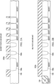
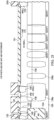
- FIG. 1A is a cross sectional depiction of an IC 100 including an example lateral junction diode device 110 with its series connected embedded diode 120 and a depletion-mode NLDMOS device 130.
- the dashed lines in FIG. 1A define the spatial extent of half-device used in FIG. 2A-2P showing a processing progression described below.
- LDMOS devices are described herein as being an NLDMOS device 130, the LDMOS device for the lateral junction diode device 110 can also be a PLDMOS device as known in the art by changing all the doping types to the other doping type.
- the IC 100 is also shown including functional circuitry 170 comprising a plurality of transistors, resistor, and capacitors configured together shown by a circuitry block that realizes and carries out a desired functionality, such as that of a digital IC (e.g., digital signal processor) or analog IC (e.g., amplifier or power converter), and in one example a BiCMOS (MOS and Bipolar) IC.
- a digital IC e.g., digital signal processor
- analog IC e.g., amplifier or power converter
- BiCMOS MOS and Bipolar
- the capability of the functional circuitry 170 provided on a described IC may vary, for example ranging from a simple device to a complex device.
- the specific functionality contained within functional circuitry 170 is not of importance to the described ICs.
- the lateral junction diode device 110 can be seen to be a 2-terminal device, with a high voltage (HV) cathode 141 doped n-type shown as 'K' as the first terminal and an anode 122 doped p-type shown as 'A' as the second terminal which is the anode for both the lateral junction diode device 110 and for the embedded diode 120.
- HV cathode' as used herein is used to distinguish the lateral junction diode device's 110 cathode which provides a higher breakdown voltage with respect to its anode which is anode 122 as compared to the cathode 121 of the embedded diode 120 with respect to its anode which is also anode 122.
- the various terminal connections for lateral junction diode device 110 are shown provided by a metal 1 (M1) layer that contacts the p-type semiconductor surface layer of the substrate 105 by filled vias (e.g., W filled vias) formed through a dielectric layer 167 on the semiconductor surface layer. Further connections are provided by another metal layer, shown as M2, that connects some M1 features shown directly connecting the anode 122 and the nwell 123 diffused into the n-buried layer (NBL) 124 underneath (n-type isolation diffusion 123/124) providing one side of the junction isolation region with the other side being the p-type semiconductor surface layer of the substrate 105, to the gate 133, and the cathode 121 of the embedded diode 120 to the n+ source 131.
- M1 metal 1
- the embedded diode 120 as shown can have a circular (racetrack) geometry and the isolation diffusion 123/124 can form a ring around the embedded diode 120.
- the isolation diffusion 123/124 can form a ring around the embedded diode 120.
- the cathode 121 couples to a p+ contact 137 formed in a first pwell 149.
- one substrate arrangement can be a p-epitaxial (epi) layer on a p-substrate.
- the epi layer can have a doping concentration sufficiently low, such as ⁇ 1 ⁇ 10 16 cm -3 or ⁇ 1 ⁇ 10 15 cm -3 , to provide the lateral junction diode device 110 a high BV.
- NLDMOS device 130 as shown has a circular (racetrack) geometry and includes a n+ source 131, an n+ drain that shares the same node as the HV cathode 141, a gate electrode 133 (e.g., a polysilicon gate) above a gate dielectric 134, and a normally on channel region 135 under the gate electrode 133 over the gate dielectric 134.
- NLDMOS 130 can be configured as a multi-finger design as well.
- An n- drift region 138/136 is in the semiconductor surface layer between the channel region 135 and the drain that shares the same node as the HV cathode 141.
- the n-buried (NB) layer drift (NBdrift) sub-regions 136a, 136b, ... are shown in FIG. 1A spaced apart representing the as-implanted distribution used to form a diluted NBdrift region, having a lower dopant concentration on the source end as compared to the doping level at the drain end.
- the respective NBdrift sub-regions 136a, 136b , ... after the heat cycling during fabrication will in the final IC all be connected together laterally and will also diffuse up near the semiconductor surface.
- the gate dielectric layer 134 can comprise silicon oxide, silicon oxynitride, or other dielectric material. In one particular aspect the gate dielectric layer 134 can comprise 200 A of silicon oxide.
- the source 131 is formed in a pwell referred to herein as a deep pwell (Dwell) 139 that provides a body region for the NLDMOS device 130, where the Dwell 139 includes a p+ contact 137.
- the p+ contact 137 to the Dwell 139 and the source 131 are shown directly connected together by vias coupled to metal 1. As described above, there is also a p+ contact 137 contacting the first pwell 149.
- the embedded diode 120 includes a cathode 121, and an anode 122 that as noted above functions as the anode for both the embedded diode 120 and for the lateral junction diode device 110.
- the embedded diode 120 as described above is junction isolated by an isolation region that includes an n-type diffusion 123/124 providing one side of the junction isolation region located between the anode 122 and the source 131 that is diffused into p-layer (e.g., a p- epi layer) on the surface of the substrate 105.
- the anode 122 and isolation region are directly connected to the gate electrode 133, such as using doped polysilicon or filled vias together with metal thereon (e.g., M1 and M2).
- the cathode 121 is directly connected to the source 131, such as by doped polysilicon or by metal.
- FIG. 1B shows an equivalent circuit for the lateral junction diode device 110 in FIG. 1A showing an embedded diode 120 in series with the depletion mode NLDMOS device 130.
- the embedded diode 120 is shown as a 7V clamp diode because the embedded diode 120 can function to clamp the gate 133 to source 131 voltage (V GS ) for the NLDMOS device 130 (as it is electrically in parallel to it) to a below ground voltage, such as at -7V, sufficient to turn off the NLDMOS device 130 despite the NLDMOS device 130 being a depletion mode device.
- V GS source 131 voltage
- the embedded diode 120 has a reverse breakdown voltage of 5 to 100 volts, such as 5 to 15 volts.
- the BV of the embedded diode 120 should not exceed the gate 133 to source 131 BV which is limited by the BV of the gate dielectric layer 134, typically being a gate oxide 150A to 1,000A thick which will typically safely sustain a voltage across it of about 5V to 30V. This voltage clamping provided is needed during the blocking mode for a bootstrap diode of a high side gate driver IC.
- the lateral junction diode device 110 functions as a two terminal device (anode 122 shown as 'A' and a HV cathode 141 shown as 'K').
- the embedded diode 120 will become forward biased at a forward voltage of about ⁇ 0.7V.
- current from the anode 122 will thus flow through the normally on channel region 135 which is an n-channel for the NLDMOS 130 device that together with the drift region extends from the S 131 to the drain (which shares the node with the HV cathode 141) since it is depletion mode device.
- the reverse blocking mode where the V at the anode 122 is ⁇ the V at the HV cathode 141 (thus reversed biased), before the voltage reaches the clamp voltage which results from a junction breakdown analogous to that of Zener diode (e.g., -7 volts), a very small amount of reverse current from the cathode 121 to anode 122 will flow.
- Zener diode e.g., -7 volts
- the embedded diode 120 functions as a voltage clamp at about -7 V because once V K , aux reaches about -7V, the embedded diode 120 will breakdown turning off the NLDMOS device 130 thus providing the function of reverse blocking.
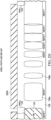
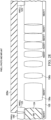
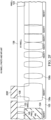
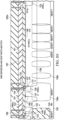
- FIGS. 2A-2P are cross-sectional diagrams showing processing progression for an example method of forming an IC including a lateral junction diode device, according to an example aspect.
- the in-process lateral junction diode device 110 and NLDMOS device 130 are shown in FIGS. 2A-2P as half-devices corresponding to the dashed lines shown in FIG. 1A to allow the features shown to be larger as they are both symmetric device components.
- FIG. 2A shows the in-process IC formed on a substrate 105 after NBdrift region photolithography and then an n-type ion implant to form the NBdrift sub-regions 136a, 136b, ....
- the NBdrift implant species can be phosphorus, at a dose from 1 ⁇ 10 12 to 1 ⁇ 10 13 cm -2 , implanted at an energy of 30 to 300 keV.
- the photoresist is shown in FIG. 2A as 205a.
- the photoresist 205a after the NBdrift implant is then stripped.
- FIG. 2B shows the in-process IC after NBL photolithography to provide photoresist 205b and then an n+ ion implant to provide the dopant to form the NBL 124.
- the NBL species can be for example phosphorus, at a dose from 5 ⁇ 10 14 to 5 ⁇ 10 15 cm -2 , implanted at an energy of 50 to 300 keV. This is followed by stripping of the photoresist 205b and then a drive-in process with a typical drive time of 30 to 60 minutes at a temperature 1150 °C to 1250 °C.
- FIG. 2C shows the in-process IC after p-type epitaxial growth to form a p-epi layer 106 on the substrate 105.
- the p-epi layer 106 is lightly doped having a typical boron doping concentration of about 1 ⁇ 10 15 cm -3 (e.g., 7 ⁇ 10 14 cm -3 to 1.4 ⁇ 10 16 cm -3 ) or equivalently a resistivity of about 10 ohm ⁇ cm (e.g., 1 to 20 ohm ⁇ cm).
- 2D shows the in-process IC after nwell photolithography showing photoresist 205d and then an ion implant to form nwells 123, which is followed by the stripping of the photoresist 205d.
- the nwell implant species can be for example phosphorus, at a dose from 1 ⁇ 10 13 to 1 ⁇ 10 15 cm -2 , implanted at an energy of 100 to 500 keV.
- FIG. 2E shows the in-process IC after pwell photolithography to provide photoresist 205e and then a boron ion implant to form a first pwell 149, followed by the stripping of the photoresist 205e.
- the first pwell species can boron, at a dose from 1 ⁇ 10 13 to 1 ⁇ 10 15 cm -2 , implanted at an energy of 50 to 200 keV.
- FIG. 2F shows the in-process IC after high voltage nwell photolithography and an ion implant to form high voltage (HV) nwells 138, which is followed by stripping of the photoresist 205f, followed by a drive-in process.
- HV high voltage
- the HV nwell implant species can be for example phosphorus, at a dose from 1 ⁇ 10 12 to 1 ⁇ 10 14 cm -2 , implanted at an energy of 100 to 800 keV, with a drive performed at 1100 °C to 1250 °C, for 100 to 500 minutes.
- FIG. 2G shows the in-process IC after active area (shown as 'MOAT') photolithography, following the etch of a silicon nitride layer over a silicon oxide layer to open the areas to receive LOCal Oxidation Of Silicon (LOCOS), photoresist stripping, then local LOCOS to form field oxide 151.
- LOCOS LOCal Oxidation Of Silicon
- FIG. 2H shows the in-process IC after a second pwell (sometimes called a deep pwell, or dwell) photolithography and dwell ion implant to form Dwells 139, then stripping of the photoresist 205h.
- a second pwell sometimes called a deep pwell, or dwell
- FIG. 2I shows the in-process IC after n-channel threshold adjust (VTN) photolithography and VTN ion implant to form VTN regions 148, then the stripping of the photoresist 205i.
- the adjust VTN species can be boron, for example at a dose from 1 ⁇ 10 12 to 1 ⁇ 10 13 cm -2 , implanted at an energy of 100 to 400 keV.
- FIG. 2J shows the in-process IC after VTP photolithography and ion implant to form VTP regions 147, then stripping of the photoresist 205j.
- the VTP implant species can be for example phosphorus, at a dose from 1 ⁇ 10 12 to 1 ⁇ 10 13 cm -2 , implanted at an energy of 10 to 300 keV. No diffusion is needed directly after this implantation.
- FIG. 2K shows the in-process IC after gate oxidation to provide a gate dielectric 134.
- the gate dielectric layer 134 can comprise silicon oxide, silicon oxynitride, or other dielectric material.
- FIG. 2L shows the in-process IC after gate polysilicon deposition to form gate 133 and gate polysilicon photolithography and patterning, and the stripping of the photoresist strip.
- the gate 133 can comprise polysilicon be formed by a low pressure chemical vapor deposition (LPCVD) step.
- LPCVD low pressure chemical vapor deposition
- the gate 133 can comprise materials other than polysilicon.
- FIG. 2M shows the in-process IC after n+ source/drain (NSD) photolithography and NSD ion implantation to form n+ regions 153 including the S 131 and the n+ contact 141a for the HV cathode 141 that also provide n+ drain for the NLDMOS device.
- the NSD implant species can for example be arsenic, at a dose from 1 ⁇ 10 14 to 5 ⁇ 10 15 cm -2 , implanted at an energy of 20 to 200 keV, which is followed by stripping of the photoresist 205m.
- FIG. 2N shows the in-process IC after p+ source/drain (PSD) photolithography and PSD ion implant to form p+ regions including p+ contacts 137 and then stripping of the photoresist.
- PSD implant species can for example be boron, at a dose from 1 ⁇ 10 14 to 5 ⁇ 10 15 cm -2 , implanted at an energy of 10 to 100 keV.
- FIG. 2O shows the in-process IC after pre-metal dielectric (PMD) deposition to form a dielectric layer 167 and contact (CONT) photolithography and etching to form contacts through the dielectric layer 167, followed by filling of the contacts to provide filled contacts 168, such as with W, and then by stripping of the photoresist 205o.
- PMD pre-metal dielectric
- CONT contact
- FIG. 2P shows the in-process IC after first metal deposition photolithography and etching to form first metal features including metal 285a as shown that provides metal contacting using filled contacts 168 to the n+ contact 141a to the HV cathode (K) 141 (which is the same node as the drain of the NLDMOS device 130) of the lateral junction diode device 110, metal 285b that provides metal contacting the gate 133 of the NLDMOS device 130, metal 285c that provides metal contacting the S 131.
- the metal also includes metal 285d contacting the anode 122 of both the lateral junction diode device 110 and the embedded diode 120, and metal 285e contacting the cathode 121 of the embedded diode 120.
- the method further includes one or more other metal levels separated by inter-level dielectric (ILD), including a second metal level that can provide the various connections between metal 1 features shown in FIG. 1A , such as gate 133 to anode 122, followed by passivation overcoat (PO) photolithography and PO etching, and then the stripping of the PO photoresist.
- ILD inter-level dielectric
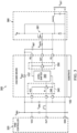
- FIG. 3 depicts a high side gate driver IC 300 including a described lateral junction diode device shown as its bootstrap diode 110' which in FIG. 3 is shown as D BST .
- the high side gate driver IC 300 is formed on a substrate 105 having at least a semiconductor surface layer.
- the high side gate driver IC 300 includes a level-shifter 330, an input (IN) pin, a VCC power supply (VCC), a high side floating supply (VB) node, and an output node (OUT).
- a ground (GND) referred low voltage controller 340 is on an input side of the level-shifter 330 and a high voltage referred driver 350 is on an output side of the level-shifter 330.
- the bootstrap diode 110' is connected between the VCC pin and the VB pin.
- the power stage being driven by the high side gate driver IC 300 is shown as 360 that includes a power switch 361.
- a controller shown as a PWM controller 320 is shown providing a PWM control signal at its OUT pin that is coupled to the high side gate driver IC 300.
- the embedded diode 120 functions as a voltage clamp at about 7 V because once the VK, aux node reaches about -7V, the embedded diode 120 will breakdown turning off the NLDMOS device 130 to provide the function of reverse voltage blocking.
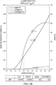
- FIGS. 4A , FIG. 4B , and FIG. 4D show example room-temperature measured current data from an example lateral junction diode device 110 formed using a process described above in FIGS. 2A-2P that evidences a high BV ( FIG. 4A ) and significantly reduced substrate leakage current ( FIGS. 4B and 4D ) as compared to the performance of a body diode of a high voltage LDMOS device alone.
- FIG. 4A shows the reverse breakdown voltage distribution for the lateral junction diode device 110 showing a median value of 845 V.
- the BV value range for the conventional high voltage LDMOS device alone should be in a similar range of about 837 V.
- FIGS. 4B and 4D represent the substrate current (Isub) to anode current (Ia) ratio (Isub/I A ) that evidences how Isub is reduced by a described lateral junction diode device.
- the I SUB /I A is reduced when compared to the I SUB /I A of 18% (almost 10 times more Isub) measured from the body diode of the high voltage LDMOS device as shown in FIG.
- the described aspects are useful to form semiconductor die that may be integrated into a variety of assembly flows to form a variety of different devices and related products.
- the semiconductor die may include various elements therein and/or layers thereon, including barrier layers, dielectric layers, device structures, active elements and passive elements including source regions, drain regions, bit lines, bases, emitters, collectors, conductive lines, conductive vias, etc.
- the semiconductor die can be formed from a variety of processes including bipolar, insulated gate bipolar transistor (IGBT), CMOS, BiCMOS and MEMS.
Landscapes
- Insulated Gate Type Field-Effect Transistor (AREA)
- Metal-Oxide And Bipolar Metal-Oxide Semiconductor Integrated Circuits (AREA)
Claims (14)
- Integrierte Schaltung (IC), beinhaltend eine Lateralübergangsdiodenvorrichtung (110), umfassend:ein Substrat (105) mit mindestens einer Halbleiteroberflächenschicht, die mit einer ersten Art dotiert ist;wobei die Lateralübergangsdiodenvorrichtung beinhaltet:einen MOSFET vom Verarmungstyp mit lateraler Diffusion (LDMOS-Vorrichtung) (130) in der Halbleiteroberflächenschicht, beinhaltend eine Source (131), die mit einer zweiten Art dotiert ist, einen Drain, der mit der zweiten Art dotiert ist, und ein Gate (133) über einem Gate-Dielektrikum (134) auf der Halbleiteroberflächenschicht, einen Kanalbereich (135), der mit der zweiten Art dotiert ist, unter dem Gate auf dem Gate-Dielektrikum, und einen Driftbereich (138/136), der mit der zweiten Art dotiert ist, zwischen dem Kanalbereich und dem Drain, wobei der Drain außerdem eine Hochspannungs-(HV)-Kathode (141) für die Lateralübergangsdiodenvorrichtung bereitstellt; undeine eingebettete Diode (120), beinhaltend eine zweite Kathode (121) und eine Anode (122), die mit der Lateralübergangsdiodenvorrichtung in der Halbleiteroberflächenschicht gemeinsam genutzt wird, wobei die eingebettete Diode durch einen Isolationsbereich (123/124 bis 105), der sich zwischen der Anode und der Source befindet, vom Übergang isoliert ist;wobei die Anode und der Isolationsbereich direkt mit dem Gate verbunden sind, und wobei die zweite Kathode direkt mit der Source verbunden ist; undwobei der Isolationsbereich direkt mit dem Gate verbunden ist und die zweite Kathode direkt mit der Source verbunden ist, und zwar beide durch eine Metallschicht (M2).
- IC nach Anspruch 1, wobei das Gate ein Polysilizium-Gate umfasst.
- Integrierte Schaltung (IC) (300) für einen High-Side-Gate-Treiber, umfassend:den High-Side-Gate-Treiber, der auf einem Substrat (105) ausgebildet ist, das mindestens eine Halbleiteroberflächenschicht beinhaltet, die mit einer ersten Art dotiert ist;einen Pegelschieber (330), beinhaltend einem Eingang, einen Stromversorgungsanschluss, einen potentialfreien High-Side-Versorgungs-(VB)-Anschluss und einen Ausgangsanschluss (OUT);einen auf Masse (GND) bezogenen Niederspannungsregler (340) auf einer Eingangsseite des Pegelschiebers und einen auf Hochspannung bezogenen Treiber (350) auf einer Ausgangsseite des Pegelschiebers, undeine Bootstrap-Diode (110'), die zwischen den Stromversorgungsanschluss und den VB-Anschluss geschaltet ist,wobei die Bootstrap-Diode eine Lateralübergangsdiodenvorrichtung (110) umfasst, umfassend:einen MOSFET vom Verarmungstyp mit lateraler Diffusion (LDMOS-Vorrichtung) (130) in der Halbleiteroberflächenschicht, beinhaltend eine Source (131), die mit einer zweiten Art dotiert ist, einen Drain, der mit der zweiten Art dotiert ist, und ein Gate (133) über einem Gate-Dielektrikum auf der Halbleiteroberflächenschicht, einen Kanalbereich (135), der mit der zweiten Art dotiert ist, unter dem Gate auf dem Gate-Dielektrikum, und einen Driftbereich (138/136), der mit der zweiten Art dotiert ist, zwischen dem Kanalbereich und dem Drain, wobei der Drain außerdem eine Hochspannungs-(HV)-Kathode (141) für die Lateralübergangsdiodenvorrichtung bereitstellt;eine eingebettete Diode (120), beinhaltend eine zweite Kathode (121) und eine Anode (122), die mit der Lateralübergangsdiodenvorrichtung in der Halbleiteroberflächenschicht gemeinsam genutzt wird, wobei die eingebettete Diode durch einen Isolationsbereich (123/124 bis 105), der eine zwischen der Anode und der Source angeordnete Isolationsdiffusion umfasst, vom Übergang isoliert ist;wobei die Anode und der Isolationsbereich direkt mit dem Gate verbunden sind, und wobei die zweite Kathode direkt mit der Source verbunden ist.
- IC nach Anspruch 1 oder IC für einen High-Side-Gate-Treiber nach Anspruch 3, wobei die Halbleiteroberflächenschicht eine p-Epitaxieschicht mit einer Dotierungskonzentration < 1,0 × 1016 cm-3 umfasst und wobei die LDMOS-Vorrichtung eine NLDMOS-Vorrichtung umfasst.
- IC nach Anspruch 1 oder High-Side-Gate-Treiber nach Anspruch 3, wobei der Driftbereich einen verdünnten Driftbereich mit niedrigerer Dotierung zur Source hin im Vergleich zu einem Dotierungsniveau zum Drain hin umfasst.
- IC nach Anspruch 4 oder High-Side-Gate-Treiber nach Anspruch 4, wobei die eingebettete Diode eine Durchbruchspannung in Sperrrichtung von 5 bis 15 Volt aufweist.
- High-Side-Gate-Treiber nach Anspruch 3, wobei der Isolationsbereich direkt mit dem Gate verbunden ist und die zweite Kathode direkt mit der Source verbunden ist, und zwar beide durch eine Metallschicht (M2).
- IC nach Anspruch 1 oder der High-Side-Gate-Treiber nach Anspruch 3, wobei die Lateralübergangsdiodenvorrichtung eine Durchbruchspannung in Sperrrichtung von mindestens 200 V bereitstellt.
- Verfahren zur Herstellung einer integrierten Schaltung (IC), umfassend:
Ausbilden einer Lateralübergangsdiodenvorrichtung (110) auf einem Substrat (105) mit einer Halbleiteroberflächenschicht, die mit einer ersten Art dotiert ist, beinhaltend:Ausbilden eines MOSFET vom Verarmungstyp mit lateraler Diffusion (LDMOS-Vorrichtung) (130) in der Halbleiteroberflächenschicht, beinhaltend eine Source (131), einen Drain und ein Gate (133) über einem Gate-Dielektrikum (134) auf der Halbleiteroberflächenschicht, einen Kanalbereich (135), der mit einer zweiten Art dotiert ist, unter dem Gate auf dem Gate-Dielektrikum, und einen Driftbereich (138/136) zwischen dem Kanalbereich (135) und dem Drain, wobei der Drain auch eine Hochspannungs-(HV)-Kathode (141) für die Lateralübergangsdiodenvorrichtung bereitstellt;Ausbilden einer eingebetteten Diode (120), beinhaltend eine zweite Kathode (121) und eine Anode (122), die mit der Lateralübergangsdiodenvorrichtung in der Halbleiteroberflächenschicht gemeinsam genutzt wird, wobei die eingebettete Diode durch einen Isolationsbereich (123/124 bis 105), der sich zwischen der Anode und der Source befindet, vom Übergang isoliert ist; unddirektes Verbinden der Anode und des Isolationsbereichs mit dem Gate und direktes Verbinden der zweiten Kathode mit der Source, beides durch Ausbilden einer Verbindung unter Verwendung einer Metallschicht (M2). - Verfahren nach Anspruch 9, wobei die Halbleiteroberflächenschicht eine p-Epitaxieschicht mit einer Dotierungskonzentration < 1,0 × 1016 cm-3 umfasst und wobei die LDMOS-Vorrichtung eine NLDMOS-Vorrichtung umfasst.
- Verfahren nach Anspruch 9, wobei der Driftbereich als verdünnter Driftbereich mit einer geringeren Dotierung in Richtung der Source im Vergleich zu einem Dotierungsniveau in Richtung des Drains ausgebildet ist.
- Verfahren nach Anspruch 9, wobei die eingebettete Diode eine Durchbruchspannung in Sperrrichtung von 5 bis 15 Volt aufweist.
- Verfahren nach Anspruch 9, wobei die Lateralübergangsdiodenvorrichtung eine Durchbruchspannung in Sperrrichtung von mindestens 200 V bereitstellt.
- Verfahren nach Anspruch 9, wobei das Gate ein Polysilizium-Gate umfasst, das durch einen chemischen Niederdruck-Gasphasenabscheidungs-(LPCVD)-Prozess gebildet wird.
Applications Claiming Priority (2)
| Application Number | Priority Date | Filing Date | Title |
|---|---|---|---|
| US15/850,854 US10559681B2 (en) | 2017-12-21 | 2017-12-21 | High voltage lateral junction diode device |
| PCT/US2018/066933 WO2019126572A1 (en) | 2017-12-21 | 2018-12-20 | High voltage lateral junction diode device |
Publications (3)
| Publication Number | Publication Date |
|---|---|
| EP3729508A1 EP3729508A1 (de) | 2020-10-28 |
| EP3729508A4 EP3729508A4 (de) | 2021-03-17 |
| EP3729508B1 true EP3729508B1 (de) | 2023-09-27 |
Family
ID=66951492
Family Applications (1)
| Application Number | Title | Priority Date | Filing Date |
|---|---|---|---|
| EP18893115.8A Active EP3729508B1 (de) | 2017-12-21 | 2018-12-20 | Hochspannungsdiodenvorrichtung mit seitlichem anschluss |
Country Status (4)
| Country | Link |
|---|---|
| US (2) | US10559681B2 (de) |
| EP (1) | EP3729508B1 (de) |
| CN (1) | CN111279477B (de) |
| WO (1) | WO2019126572A1 (de) |
Families Citing this family (4)
| Publication number | Priority date | Publication date | Assignee | Title |
|---|---|---|---|---|
| US10559681B2 (en) * | 2017-12-21 | 2020-02-11 | Texas Instruments Incorporated | High voltage lateral junction diode device |
| US11579645B2 (en) * | 2019-06-21 | 2023-02-14 | Wolfspeed, Inc. | Device design for short-circuitry protection circuitry within transistors |
| US11355628B2 (en) * | 2019-11-17 | 2022-06-07 | Littelfuse, Inc. | Semiconductor device having junction termination structure and method of formation |
| US20240063777A1 (en) * | 2022-08-19 | 2024-02-22 | Alpha And Omega Semiconductor International Lp | Hvic device with combined level shifter and boost diode in junction termination region |
Family Cites Families (12)
| Publication number | Priority date | Publication date | Assignee | Title |
|---|---|---|---|---|
| JPS57198414A (en) | 1981-05-31 | 1982-12-06 | Takumi Tomijima | Polarizer |
| EP1699084B1 (de) | 1995-04-12 | 2011-05-25 | Fuji Electric Systems Co., Ltd. | Integrierter Hochspannungsschaltkreis, Hochspannungsübergangsabschluss- struktur und MIS-Hochspannungstransistor |
| US7719054B2 (en) * | 2006-05-31 | 2010-05-18 | Advanced Analogic Technologies, Inc. | High-voltage lateral DMOS device |
| CN1311560C (zh) * | 2003-10-16 | 2007-04-18 | 电子科技大学 | 横向低侧高压器件及高侧高压器件 |
| US7045830B1 (en) | 2004-12-07 | 2006-05-16 | Fairchild Semiconductor Corporation | High-voltage diodes formed in advanced power integrated circuit devices |
| US7608907B2 (en) | 2005-01-06 | 2009-10-27 | Micrel, Inc. | LDMOS gate controlled schottky diode |
| US7842968B2 (en) | 2008-01-09 | 2010-11-30 | Fairchild Semiconductor Corporation | Integrated low leakage diode |
| JP5499877B2 (ja) * | 2010-04-23 | 2014-05-21 | 三菱電機株式会社 | 電力用半導体装置 |
| US9245998B2 (en) | 2013-12-29 | 2016-01-26 | Texas Instruments Incorporated | High voltage multiple channel LDMOS |
| GB2530284A (en) | 2014-09-17 | 2016-03-23 | Anvil Semiconductors Ltd | High voltage semiconductor devices |
| US10037028B2 (en) * | 2015-07-24 | 2018-07-31 | The Trustees Of The University Of Pennsylvania | Systems, devices, and methods for on-board sensing and control of micro aerial vehicles |
| US10559681B2 (en) * | 2017-12-21 | 2020-02-11 | Texas Instruments Incorporated | High voltage lateral junction diode device |
-
2017
- 2017-12-21 US US15/850,854 patent/US10559681B2/en active Active
-
2018
- 2018-12-20 EP EP18893115.8A patent/EP3729508B1/de active Active
- 2018-12-20 CN CN201880070022.1A patent/CN111279477B/zh active Active
- 2018-12-20 WO PCT/US2018/066933 patent/WO2019126572A1/en not_active Ceased
-
2020
- 2020-01-30 US US16/776,544 patent/US11322610B2/en active Active
Also Published As
| Publication number | Publication date |
|---|---|
| CN111279477B (zh) | 2024-08-09 |
| EP3729508A1 (de) | 2020-10-28 |
| US11322610B2 (en) | 2022-05-03 |
| EP3729508A4 (de) | 2021-03-17 |
| US20190198666A1 (en) | 2019-06-27 |
| WO2019126572A1 (en) | 2019-06-27 |
| US20200168733A1 (en) | 2020-05-28 |
| US10559681B2 (en) | 2020-02-11 |
| CN111279477A (zh) | 2020-06-12 |
Similar Documents
| Publication | Publication Date | Title |
|---|---|---|
| CN101542697B (zh) | 高压双极-cmos-dmos集成电路器件及其模块形成方法 | |
| EP1436846B1 (de) | Mos-anordnungen und entsprechende herstellungsverfahren und schaltungen | |
| US6979875B2 (en) | Reduced surface field technique for semiconductor devices | |
| KR101303405B1 (ko) | 절연 트랜지스터 및 다이오드 | |
| US11322610B2 (en) | High voltage lateral junction diode device | |
| US11183495B2 (en) | Power semiconductor devices | |
| US9048132B2 (en) | Lateral double diffused metal oxide semiconductor device and method for manufacturing the same | |
| KR101452619B1 (ko) | 부트스트랩 전계효과 트랜지스터 및 그 제조 방법 | |
| CN103797572A (zh) | 高耐压半导体装置 | |
| US20100163990A1 (en) | Lateral Double Diffused Metal Oxide Semiconductor Device | |
| EP2782130A1 (de) | Hochspannungsresistente halbleitervorrichtung | |
| US20120049271A1 (en) | Semiconductor device with high-breakdown-voltage transistor | |
| US20100032757A1 (en) | Bi-directional dmos with common drain | |
| CN106486480A (zh) | 半导体器件 | |
| CN111279488B (zh) | 高电压漏极延伸式mos晶体管 | |
| TWI629785B (zh) | 高電壓積體電路的高電壓終端結構 | |
| US8692327B2 (en) | Lateral double diffused metal oxide semiconductor device and method for manufacturing the same | |
| WO2007011354A1 (en) | Drain-extended mosfets with diode clamp | |
| CN116487442A (zh) | 二极管结构及半导体装置 | |
| TWI396180B (zh) | 單元電晶體及積體電路 | |
| TWI575741B (zh) | 高壓半導體裝置及其製造方法 | |
| US11282954B2 (en) | LDMOS device with integrated P-N junction diodes | |
| CN101263607A (zh) | 具有二极管钳位的漏极扩展mosfet | |
| TW202329458A (zh) | 二極體結構及半導體裝置 | |
| Disney et al. | 30V high-side N-channel lateral trench MOSFET |
Legal Events
| Date | Code | Title | Description |
|---|---|---|---|
| STAA | Information on the status of an ep patent application or granted ep patent |
Free format text: STATUS: THE INTERNATIONAL PUBLICATION HAS BEEN MADE |
|
| PUAI | Public reference made under article 153(3) epc to a published international application that has entered the european phase |
Free format text: ORIGINAL CODE: 0009012 |
|
| STAA | Information on the status of an ep patent application or granted ep patent |
Free format text: STATUS: REQUEST FOR EXAMINATION WAS MADE |
|
| 17P | Request for examination filed |
Effective date: 20200721 |
|
| AK | Designated contracting states |
Kind code of ref document: A1 Designated state(s): AL AT BE BG CH CY CZ DE DK EE ES FI FR GB GR HR HU IE IS IT LI LT LU LV MC MK MT NL NO PL PT RO RS SE SI SK SM TR |
|
| AX | Request for extension of the european patent |
Extension state: BA ME |
|
| A4 | Supplementary search report drawn up and despatched |
Effective date: 20210211 |
|
| RIC1 | Information provided on ipc code assigned before grant |
Ipc: H01L 29/08 20060101ALI20210205BHEP Ipc: H01L 29/78 20060101ALI20210205BHEP Ipc: H01L 21/761 20060101ALI20210205BHEP Ipc: H01L 29/423 20060101ALI20210205BHEP Ipc: H03K 17/06 20060101ALI20210205BHEP Ipc: H01L 29/861 20060101ALI20210205BHEP Ipc: H01L 29/06 20060101ALI20210205BHEP Ipc: H01L 29/10 20060101ALI20210205BHEP Ipc: H01L 29/66 20060101ALI20210205BHEP Ipc: H01L 27/06 20060101AFI20210205BHEP Ipc: H01L 27/07 20060101ALI20210205BHEP |
|
| DAV | Request for validation of the european patent (deleted) | ||
| DAX | Request for extension of the european patent (deleted) | ||
| GRAP | Despatch of communication of intention to grant a patent |
Free format text: ORIGINAL CODE: EPIDOSNIGR1 |
|
| STAA | Information on the status of an ep patent application or granted ep patent |
Free format text: STATUS: GRANT OF PATENT IS INTENDED |
|
| INTG | Intention to grant announced |
Effective date: 20230509 |
|
| P01 | Opt-out of the competence of the unified patent court (upc) registered |
Effective date: 20230523 |
|
| GRAS | Grant fee paid |
Free format text: ORIGINAL CODE: EPIDOSNIGR3 |
|
| GRAA | (expected) grant |
Free format text: ORIGINAL CODE: 0009210 |
|
| STAA | Information on the status of an ep patent application or granted ep patent |
Free format text: STATUS: THE PATENT HAS BEEN GRANTED |
|
| AK | Designated contracting states |
Kind code of ref document: B1 Designated state(s): AL AT BE BG CH CY CZ DE DK EE ES FI FR GB GR HR HU IE IS IT LI LT LU LV MC MK MT NL NO PL PT RO RS SE SI SK SM TR |
|
| REG | Reference to a national code |
Ref country code: GB Ref legal event code: FG4D |
|
| REG | Reference to a national code |
Ref country code: CH Ref legal event code: EP |
|
| REG | Reference to a national code |
Ref country code: DE Ref legal event code: R096 Ref document number: 602018058456 Country of ref document: DE |
|
| REG | Reference to a national code |
Ref country code: IE Ref legal event code: FG4D |
|
| REG | Reference to a national code |
Ref country code: LT Ref legal event code: MG9D |
|
| PG25 | Lapsed in a contracting state [announced via postgrant information from national office to epo] |
Ref country code: GR Free format text: LAPSE BECAUSE OF FAILURE TO SUBMIT A TRANSLATION OF THE DESCRIPTION OR TO PAY THE FEE WITHIN THE PRESCRIBED TIME-LIMIT Effective date: 20231228 |
|
| PG25 | Lapsed in a contracting state [announced via postgrant information from national office to epo] |
Ref country code: SE Free format text: LAPSE BECAUSE OF FAILURE TO SUBMIT A TRANSLATION OF THE DESCRIPTION OR TO PAY THE FEE WITHIN THE PRESCRIBED TIME-LIMIT Effective date: 20230927 Ref country code: RS Free format text: LAPSE BECAUSE OF FAILURE TO SUBMIT A TRANSLATION OF THE DESCRIPTION OR TO PAY THE FEE WITHIN THE PRESCRIBED TIME-LIMIT Effective date: 20230927 Ref country code: NO Free format text: LAPSE BECAUSE OF FAILURE TO SUBMIT A TRANSLATION OF THE DESCRIPTION OR TO PAY THE FEE WITHIN THE PRESCRIBED TIME-LIMIT Effective date: 20231227 Ref country code: LV Free format text: LAPSE BECAUSE OF FAILURE TO SUBMIT A TRANSLATION OF THE DESCRIPTION OR TO PAY THE FEE WITHIN THE PRESCRIBED TIME-LIMIT Effective date: 20230927 Ref country code: LT Free format text: LAPSE BECAUSE OF FAILURE TO SUBMIT A TRANSLATION OF THE DESCRIPTION OR TO PAY THE FEE WITHIN THE PRESCRIBED TIME-LIMIT Effective date: 20230927 Ref country code: HR Free format text: LAPSE BECAUSE OF FAILURE TO SUBMIT A TRANSLATION OF THE DESCRIPTION OR TO PAY THE FEE WITHIN THE PRESCRIBED TIME-LIMIT Effective date: 20230927 Ref country code: GR Free format text: LAPSE BECAUSE OF FAILURE TO SUBMIT A TRANSLATION OF THE DESCRIPTION OR TO PAY THE FEE WITHIN THE PRESCRIBED TIME-LIMIT Effective date: 20231228 Ref country code: FI Free format text: LAPSE BECAUSE OF FAILURE TO SUBMIT A TRANSLATION OF THE DESCRIPTION OR TO PAY THE FEE WITHIN THE PRESCRIBED TIME-LIMIT Effective date: 20230927 |
|
| REG | Reference to a national code |
Ref country code: NL Ref legal event code: MP Effective date: 20230927 |
|
| REG | Reference to a national code |
Ref country code: AT Ref legal event code: MK05 Ref document number: 1616297 Country of ref document: AT Kind code of ref document: T Effective date: 20230927 |
|
| PG25 | Lapsed in a contracting state [announced via postgrant information from national office to epo] |
Ref country code: NL Free format text: LAPSE BECAUSE OF FAILURE TO SUBMIT A TRANSLATION OF THE DESCRIPTION OR TO PAY THE FEE WITHIN THE PRESCRIBED TIME-LIMIT Effective date: 20230927 |
|
| PG25 | Lapsed in a contracting state [announced via postgrant information from national office to epo] |
Ref country code: IS Free format text: LAPSE BECAUSE OF FAILURE TO SUBMIT A TRANSLATION OF THE DESCRIPTION OR TO PAY THE FEE WITHIN THE PRESCRIBED TIME-LIMIT Effective date: 20240127 |
|
| PG25 | Lapsed in a contracting state [announced via postgrant information from national office to epo] |
Ref country code: AT Free format text: LAPSE BECAUSE OF FAILURE TO SUBMIT A TRANSLATION OF THE DESCRIPTION OR TO PAY THE FEE WITHIN THE PRESCRIBED TIME-LIMIT Effective date: 20230927 |
|
| PG25 | Lapsed in a contracting state [announced via postgrant information from national office to epo] |
Ref country code: ES Free format text: LAPSE BECAUSE OF FAILURE TO SUBMIT A TRANSLATION OF THE DESCRIPTION OR TO PAY THE FEE WITHIN THE PRESCRIBED TIME-LIMIT Effective date: 20230927 |
|
| PG25 | Lapsed in a contracting state [announced via postgrant information from national office to epo] |
Ref country code: SM Free format text: LAPSE BECAUSE OF FAILURE TO SUBMIT A TRANSLATION OF THE DESCRIPTION OR TO PAY THE FEE WITHIN THE PRESCRIBED TIME-LIMIT Effective date: 20230927 Ref country code: RO Free format text: LAPSE BECAUSE OF FAILURE TO SUBMIT A TRANSLATION OF THE DESCRIPTION OR TO PAY THE FEE WITHIN THE PRESCRIBED TIME-LIMIT Effective date: 20230927 Ref country code: IS Free format text: LAPSE BECAUSE OF FAILURE TO SUBMIT A TRANSLATION OF THE DESCRIPTION OR TO PAY THE FEE WITHIN THE PRESCRIBED TIME-LIMIT Effective date: 20240127 Ref country code: ES Free format text: LAPSE BECAUSE OF FAILURE TO SUBMIT A TRANSLATION OF THE DESCRIPTION OR TO PAY THE FEE WITHIN THE PRESCRIBED TIME-LIMIT Effective date: 20230927 Ref country code: EE Free format text: LAPSE BECAUSE OF FAILURE TO SUBMIT A TRANSLATION OF THE DESCRIPTION OR TO PAY THE FEE WITHIN THE PRESCRIBED TIME-LIMIT Effective date: 20230927 Ref country code: CZ Free format text: LAPSE BECAUSE OF FAILURE TO SUBMIT A TRANSLATION OF THE DESCRIPTION OR TO PAY THE FEE WITHIN THE PRESCRIBED TIME-LIMIT Effective date: 20230927 Ref country code: AT Free format text: LAPSE BECAUSE OF FAILURE TO SUBMIT A TRANSLATION OF THE DESCRIPTION OR TO PAY THE FEE WITHIN THE PRESCRIBED TIME-LIMIT Effective date: 20230927 Ref country code: SK Free format text: LAPSE BECAUSE OF FAILURE TO SUBMIT A TRANSLATION OF THE DESCRIPTION OR TO PAY THE FEE WITHIN THE PRESCRIBED TIME-LIMIT Effective date: 20230927 Ref country code: PT Free format text: LAPSE BECAUSE OF FAILURE TO SUBMIT A TRANSLATION OF THE DESCRIPTION OR TO PAY THE FEE WITHIN THE PRESCRIBED TIME-LIMIT Effective date: 20240129 |
|
| PG25 | Lapsed in a contracting state [announced via postgrant information from national office to epo] |
Ref country code: PL Free format text: LAPSE BECAUSE OF FAILURE TO SUBMIT A TRANSLATION OF THE DESCRIPTION OR TO PAY THE FEE WITHIN THE PRESCRIBED TIME-LIMIT Effective date: 20230927 Ref country code: IT Free format text: LAPSE BECAUSE OF FAILURE TO SUBMIT A TRANSLATION OF THE DESCRIPTION OR TO PAY THE FEE WITHIN THE PRESCRIBED TIME-LIMIT Effective date: 20230927 |
|
| REG | Reference to a national code |
Ref country code: DE Ref legal event code: R097 Ref document number: 602018058456 Country of ref document: DE |
|
| PG25 | Lapsed in a contracting state [announced via postgrant information from national office to epo] |
Ref country code: DK Free format text: LAPSE BECAUSE OF FAILURE TO SUBMIT A TRANSLATION OF THE DESCRIPTION OR TO PAY THE FEE WITHIN THE PRESCRIBED TIME-LIMIT Effective date: 20230927 |
|
| PG25 | Lapsed in a contracting state [announced via postgrant information from national office to epo] |
Ref country code: DK Free format text: LAPSE BECAUSE OF FAILURE TO SUBMIT A TRANSLATION OF THE DESCRIPTION OR TO PAY THE FEE WITHIN THE PRESCRIBED TIME-LIMIT Effective date: 20230927 |
|
| REG | Reference to a national code |
Ref country code: CH Ref legal event code: PL |
|
| PLBE | No opposition filed within time limit |
Free format text: ORIGINAL CODE: 0009261 |
|
| STAA | Information on the status of an ep patent application or granted ep patent |
Free format text: STATUS: NO OPPOSITION FILED WITHIN TIME LIMIT |
|
| PG25 | Lapsed in a contracting state [announced via postgrant information from national office to epo] |
Ref country code: LU Free format text: LAPSE BECAUSE OF NON-PAYMENT OF DUE FEES Effective date: 20231220 |
|
| PG25 | Lapsed in a contracting state [announced via postgrant information from national office to epo] |
Ref country code: MC Free format text: LAPSE BECAUSE OF FAILURE TO SUBMIT A TRANSLATION OF THE DESCRIPTION OR TO PAY THE FEE WITHIN THE PRESCRIBED TIME-LIMIT Effective date: 20230927 |
|
| REG | Reference to a national code |
Ref country code: BE Ref legal event code: MM Effective date: 20231231 |
|
| PG25 | Lapsed in a contracting state [announced via postgrant information from national office to epo] |
Ref country code: MC Free format text: LAPSE BECAUSE OF FAILURE TO SUBMIT A TRANSLATION OF THE DESCRIPTION OR TO PAY THE FEE WITHIN THE PRESCRIBED TIME-LIMIT Effective date: 20230927 Ref country code: LU Free format text: LAPSE BECAUSE OF NON-PAYMENT OF DUE FEES Effective date: 20231220 |
|
| 26N | No opposition filed |
Effective date: 20240628 |
|
| REG | Reference to a national code |
Ref country code: IE Ref legal event code: MM4A |
|
| PG25 | Lapsed in a contracting state [announced via postgrant information from national office to epo] |
Ref country code: IE Free format text: LAPSE BECAUSE OF NON-PAYMENT OF DUE FEES Effective date: 20231220 |
|
| PG25 | Lapsed in a contracting state [announced via postgrant information from national office to epo] |
Ref country code: BE Free format text: LAPSE BECAUSE OF NON-PAYMENT OF DUE FEES Effective date: 20231231 |
|
| PG25 | Lapsed in a contracting state [announced via postgrant information from national office to epo] |
Ref country code: CH Free format text: LAPSE BECAUSE OF NON-PAYMENT OF DUE FEES Effective date: 20231231 |
|
| PG25 | Lapsed in a contracting state [announced via postgrant information from national office to epo] |
Ref country code: SI Free format text: LAPSE BECAUSE OF FAILURE TO SUBMIT A TRANSLATION OF THE DESCRIPTION OR TO PAY THE FEE WITHIN THE PRESCRIBED TIME-LIMIT Effective date: 20230927 |
|
| PG25 | Lapsed in a contracting state [announced via postgrant information from national office to epo] |
Ref country code: SI Free format text: LAPSE BECAUSE OF FAILURE TO SUBMIT A TRANSLATION OF THE DESCRIPTION OR TO PAY THE FEE WITHIN THE PRESCRIBED TIME-LIMIT Effective date: 20230927 Ref country code: IE Free format text: LAPSE BECAUSE OF NON-PAYMENT OF DUE FEES Effective date: 20231220 Ref country code: CH Free format text: LAPSE BECAUSE OF NON-PAYMENT OF DUE FEES Effective date: 20231231 Ref country code: BE Free format text: LAPSE BECAUSE OF NON-PAYMENT OF DUE FEES Effective date: 20231231 |
|
| PG25 | Lapsed in a contracting state [announced via postgrant information from national office to epo] |
Ref country code: BG Free format text: LAPSE BECAUSE OF FAILURE TO SUBMIT A TRANSLATION OF THE DESCRIPTION OR TO PAY THE FEE WITHIN THE PRESCRIBED TIME-LIMIT Effective date: 20230927 |
|
| REG | Reference to a national code |
Ref country code: DE Ref legal event code: R079 Ref document number: 602018058456 Country of ref document: DE Free format text: PREVIOUS MAIN CLASS: H01L0027060000 Ipc: H10D0084000000 |
|
| PG25 | Lapsed in a contracting state [announced via postgrant information from national office to epo] |
Ref country code: BG Free format text: LAPSE BECAUSE OF FAILURE TO SUBMIT A TRANSLATION OF THE DESCRIPTION OR TO PAY THE FEE WITHIN THE PRESCRIBED TIME-LIMIT Effective date: 20230927 |
|
| PG25 | Lapsed in a contracting state [announced via postgrant information from national office to epo] |
Ref country code: CY Free format text: LAPSE BECAUSE OF FAILURE TO SUBMIT A TRANSLATION OF THE DESCRIPTION OR TO PAY THE FEE WITHIN THE PRESCRIBED TIME-LIMIT; INVALID AB INITIO Effective date: 20181220 |
|
| PG25 | Lapsed in a contracting state [announced via postgrant information from national office to epo] |
Ref country code: HU Free format text: LAPSE BECAUSE OF FAILURE TO SUBMIT A TRANSLATION OF THE DESCRIPTION OR TO PAY THE FEE WITHIN THE PRESCRIBED TIME-LIMIT; INVALID AB INITIO Effective date: 20181220 |
|
| PG25 | Lapsed in a contracting state [announced via postgrant information from national office to epo] |
Ref country code: TR Free format text: LAPSE BECAUSE OF FAILURE TO SUBMIT A TRANSLATION OF THE DESCRIPTION OR TO PAY THE FEE WITHIN THE PRESCRIBED TIME-LIMIT Effective date: 20230927 |
|
| PGFP | Annual fee paid to national office [announced via postgrant information from national office to epo] |
Ref country code: DE Payment date: 20251126 Year of fee payment: 8 |
|
| PGFP | Annual fee paid to national office [announced via postgrant information from national office to epo] |
Ref country code: GB Payment date: 20251119 Year of fee payment: 8 |
|
| PGFP | Annual fee paid to national office [announced via postgrant information from national office to epo] |
Ref country code: FR Payment date: 20251119 Year of fee payment: 8 |