EP3729279B1 - A unified memory organization for neural network processors - Google Patents
A unified memory organization for neural network processors Download PDFInfo
- Publication number
- EP3729279B1 EP3729279B1 EP18890583.0A EP18890583A EP3729279B1 EP 3729279 B1 EP3729279 B1 EP 3729279B1 EP 18890583 A EP18890583 A EP 18890583A EP 3729279 B1 EP3729279 B1 EP 3729279B1
- Authority
- EP
- European Patent Office
- Prior art keywords
- data
- storage
- private
- shared
- unified
- Prior art date
- Legal status (The legal status is an assumption and is not a legal conclusion. Google has not performed a legal analysis and makes no representation as to the accuracy of the status listed.)
- Active
Links
Images


Classifications
-
- G—PHYSICS
- G06—COMPUTING OR CALCULATING; COUNTING
- G06F—ELECTRIC DIGITAL DATA PROCESSING
- G06F12/00—Accessing, addressing or allocating within memory systems or architectures
- G06F12/02—Addressing or allocation; Relocation
- G06F12/0207—Addressing or allocation; Relocation with multidimensional access, e.g. row/column, matrix
-
- G—PHYSICS
- G06—COMPUTING OR CALCULATING; COUNTING
- G06F—ELECTRIC DIGITAL DATA PROCESSING
- G06F12/00—Accessing, addressing or allocating within memory systems or architectures
- G06F12/02—Addressing or allocation; Relocation
- G06F12/08—Addressing or allocation; Relocation in hierarchically structured memory systems, e.g. virtual memory systems
- G06F12/0802—Addressing of a memory level in which the access to the desired data or data block requires associative addressing means, e.g. caches
- G06F12/0806—Multiuser, multiprocessor or multiprocessing cache systems
- G06F12/0813—Multiuser, multiprocessor or multiprocessing cache systems with a network or matrix configuration
-
- G—PHYSICS
- G06—COMPUTING OR CALCULATING; COUNTING
- G06F—ELECTRIC DIGITAL DATA PROCESSING
- G06F12/00—Accessing, addressing or allocating within memory systems or architectures
- G06F12/02—Addressing or allocation; Relocation
- G06F12/0223—User address space allocation, e.g. contiguous or non contiguous base addressing
- G06F12/0284—Multiple user address space allocation, e.g. using different base addresses
-
- G—PHYSICS
- G06—COMPUTING OR CALCULATING; COUNTING
- G06F—ELECTRIC DIGITAL DATA PROCESSING
- G06F12/00—Accessing, addressing or allocating within memory systems or architectures
- G06F12/02—Addressing or allocation; Relocation
- G06F12/06—Addressing a physical block of locations, e.g. base addressing, module addressing, memory dedication
- G06F12/0646—Configuration or reconfiguration
- G06F12/0692—Multiconfiguration, e.g. local and global addressing
-
- G—PHYSICS
- G06—COMPUTING OR CALCULATING; COUNTING
- G06F—ELECTRIC DIGITAL DATA PROCESSING
- G06F12/00—Accessing, addressing or allocating within memory systems or architectures
- G06F12/02—Addressing or allocation; Relocation
- G06F12/08—Addressing or allocation; Relocation in hierarchically structured memory systems, e.g. virtual memory systems
- G06F12/0802—Addressing of a memory level in which the access to the desired data or data block requires associative addressing means, e.g. caches
- G06F12/0806—Multiuser, multiprocessor or multiprocessing cache systems
- G06F12/084—Multiuser, multiprocessor or multiprocessing cache systems with a shared cache
-
- G—PHYSICS
- G06—COMPUTING OR CALCULATING; COUNTING
- G06F—ELECTRIC DIGITAL DATA PROCESSING
- G06F12/00—Accessing, addressing or allocating within memory systems or architectures
- G06F12/02—Addressing or allocation; Relocation
- G06F12/08—Addressing or allocation; Relocation in hierarchically structured memory systems, e.g. virtual memory systems
- G06F12/0802—Addressing of a memory level in which the access to the desired data or data block requires associative addressing means, e.g. caches
- G06F12/0806—Multiuser, multiprocessor or multiprocessing cache systems
- G06F12/0842—Multiuser, multiprocessor or multiprocessing cache systems for multiprocessing or multitasking
-
- G—PHYSICS
- G06—COMPUTING OR CALCULATING; COUNTING
- G06F—ELECTRIC DIGITAL DATA PROCESSING
- G06F9/00—Arrangements for program control, e.g. control units
- G06F9/06—Arrangements for program control, e.g. control units using stored programs, i.e. using an internal store of processing equipment to receive or retain programs
- G06F9/30—Arrangements for executing machine instructions, e.g. instruction decode
- G06F9/30003—Arrangements for executing specific machine instructions
- G06F9/3004—Arrangements for executing specific machine instructions to perform operations on memory
- G06F9/30043—LOAD or STORE instructions; Clear instruction
-
- G—PHYSICS
- G06—COMPUTING OR CALCULATING; COUNTING
- G06N—COMPUTING ARRANGEMENTS BASED ON SPECIFIC COMPUTATIONAL MODELS
- G06N3/00—Computing arrangements based on biological models
- G06N3/02—Neural networks
- G06N3/06—Physical realisation, i.e. hardware implementation of neural networks, neurons or parts of neurons
- G06N3/063—Physical realisation, i.e. hardware implementation of neural networks, neurons or parts of neurons using electronic means
-
- G—PHYSICS
- G11—INFORMATION STORAGE
- G11C—STATIC STORES
- G11C11/00—Digital stores characterised by the use of particular electric or magnetic storage elements; Storage elements therefor
- G11C11/54—Digital stores characterised by the use of particular electric or magnetic storage elements; Storage elements therefor using elements simulating biological cells, e.g. neuron
-
- G—PHYSICS
- G06—COMPUTING OR CALCULATING; COUNTING
- G06F—ELECTRIC DIGITAL DATA PROCESSING
- G06F2212/00—Indexing scheme relating to accessing, addressing or allocation within memory systems or architectures
- G06F2212/10—Providing a specific technical effect
- G06F2212/1016—Performance improvement
- G06F2212/1024—Latency reduction
-
- G—PHYSICS
- G06—COMPUTING OR CALCULATING; COUNTING
- G06F—ELECTRIC DIGITAL DATA PROCESSING
- G06F2212/00—Indexing scheme relating to accessing, addressing or allocation within memory systems or architectures
- G06F2212/10—Providing a specific technical effect
- G06F2212/1028—Power efficiency
-
- Y—GENERAL TAGGING OF NEW TECHNOLOGICAL DEVELOPMENTS; GENERAL TAGGING OF CROSS-SECTIONAL TECHNOLOGIES SPANNING OVER SEVERAL SECTIONS OF THE IPC; TECHNICAL SUBJECTS COVERED BY FORMER USPC CROSS-REFERENCE ART COLLECTIONS [XRACs] AND DIGESTS
- Y02—TECHNOLOGIES OR APPLICATIONS FOR MITIGATION OR ADAPTATION AGAINST CLIMATE CHANGE
- Y02D—CLIMATE CHANGE MITIGATION TECHNOLOGIES IN INFORMATION AND COMMUNICATION TECHNOLOGIES [ICT], I.E. INFORMATION AND COMMUNICATION TECHNOLOGIES AIMING AT THE REDUCTION OF THEIR OWN ENERGY USE
- Y02D10/00—Energy efficient computing, e.g. low power processors, power management or thermal management
Definitions
- CPU/GPU Central Processing Unit/Graphics Processing Unit
- SIMD Single Instruction Multiple Data
- each of the parallel multiple processing units Arithmetic Logic Units (ALUs) or small CPUs, compute simultaneously with their own data - generally 2 or 3 input operands and 1 output result. These data are stored in memory and are accessed independently in parallel.
- each processing unit can have a dedicated partition of memory and dedicated access ports to the partitions of memory.
- ALUs Arithmetic Logic Units
- many algorithms have some shared data, which can be stored in some shared memory (to save storage cost) and be broadcasted to all processing units as one of the operands.
- US 2012/075319 A1 relates to a technique for addressing data in a hierarchical graphics processing unit cluster.
- a hierarchical address is constructed based on the location of a storage circuit where a target unit of data resides.
- the hierarchical address comprises a level field indicating a hierarchical level for the unit of data and a node identifier that indicates which GPU within the GPU cluster currently stores the unit of data.
- the hierarchical address may further comprise one or more identifiers that indicate which storage circuit in a particular hierarchical level currently stores the unit of data.
- the hierarchical address is constructed and interpreted based on the level field.
- US 2011/078406 A1 relates to a technique for unifying the addressing of multiple distinct parallel memory spaces into a single address space for a thread.
- a unified memory space address is converted into an address that accesses one of the parallel memory spaces for that thread.
- a single type of load or store instruction is used that specifies the unified memory space address for a thread instead of using a different type of load or store instruction to access each of the distinct parallel memory spaces.
- US 2015/248353 A1 discloses a plurality of processing elements (PEs) including memory local to at least one of the processing elements in a data packet-switched network interconnecting the processing elements and the memory to enable any of the PEs to access the memory.
- the network consists of nodes arranged linearly or in a grid to connect the PEs and their local memories to a common controller.
- the processor performs memory accesses on data stored in the memory in response to control signals sent by the controller to the memory.
- the local memories share the same memory map or space.
- the packet-switched network supports multiple concurrent transfers between PEs and memory.
- US 2003/200378 A1 discloses local addressing for a processing element array by partitioning a register file memory (e.g., data columns, data rows), and adding a select column or row to be associated with each block.
- the select column or row allows each processing element to read data from or to write data to a different register file address.
- Global addressing may also be implemented by reading data from or writing data to the same register file address for each processing element.
- EP 3035204 A1 discloses a storage device and method for performing convolution operations.
- One embodiment of an apparatus to perform convolution operations comprises a plurality of processing units to execute convolution operations on input data and partial results; a unified scratchpad memory comprising a plurality of memory banks communicatively coupled to the plurality of processing units through a plurality of read/write ports, each of the plurality of memory banks partitioned to store both the input data and partial results; a control unit to allocate the input data and partial results to the memory banks to ensure a minimum quality of service in accordance with the specified number of read/write ports and the specified convolution operation to be performed.
- US 2016/283399 A1 discloses a technique in which a shared memory controller receives, from a computing node, a request associated with a memory transaction involving a particular line in a memory pool.
- the request includes a node address according to an address map of the computing node.
- An address translation structure is used to translate the first address into a corresponding second address according to a global address map for the memory pool, and the shared memory controller determines that a particular one of a plurality of shared memory controllers is associated with the second address in the global address map and causes the particular shared memory controller to handle the request.
- US 2016/232107 A1 discloses a hierarchical complexity for coherence protocols associated with clustered cache architectures which can be encapsulated in a simple function, i.e., that of determining when a data block is shared entirely within a cluster (i.e., a sub-tree of the hierarchy) and is private from the outside.
- GB 2 543 520 A discloses a data processing system which includes an instruction decoder which decodes protected memory access instructions (LDR/STR) and less-protected memory access instructions (LDNPR/STNPR) to generate control signals for controlling a load store unit.
- LDR/STR protected memory access instructions
- LDNPR/STNPR less-protected memory access instructions
- Embodiments of this disclosure provide a unified memory apparatus.
- the unified memory apparatus can include a unified storage medium including a first storage module having a first plurality of storage cells configured to store data, the first plurality of storage cells identified by a unique cell identifier, and a second storage module having a second plurality of storage cells configured to store data, the second plurality of storage cells identified by a unique cell identifier.
- the unified memory architecture can also include a processing unit in communication with the unified storage medium. The processing unit can be configured to receive a first input data from one of the first plurality of storage cells, receive a second input data from one of the second plurality of storage cells, and generate an output data based on the first and second input data.
- the unified storage medium can include a first storage module having a first plurality of storage cells configured to store data, the first plurality of storage cells identified by a unique cell identifier, and a second storage module having a second plurality of storage cells configured to store data, the second plurality of storage cells identified by a unique cell identifier.
- Some embodiments of this disclosure provide a method for organizing data in a unified memory apparatus having a unified storage medium and one or more processing units.
- the method can include configuring a first storage module of the unified storage medium to communicate with the one or more processing units and to include a first plurality of storage cells that are configured to store data, the first plurality of storage cells identified by a unique cell identifier.
- the method can also include configuring a second storage module of the unified storage medium to communicate with the one or more processing units and to include a second plurality of storage cells that are configured to store data, the second plurality of storage cells identified by a unique cell identifier.
- the method further includes configuring a processing unit of the one or more processing units to receive a first input data from one of the first plurality of storage cells, receive a second input data from one of the second plurality of storage cells, and generate an output data based on the first and second input data.
- Some embodiments of this disclosure provide a method for organizing data in a unified storage medium having a first storage module and a second storage module.
- the method can include configuring the first storage module of the unified storage medium to communicate with one or more processing units and to include a first plurality of storage cells that are configured to store data, the first plurality of storage cells identified by a unique cell identifier, and configuring the second storage module of the unified storage medium to communicate with one or more processing units and to include a second plurality of storage cells that are configured to store data, the second plurality of storage cells identified by a unique cell identifier.
- the unique cell identifier of the first and second plurality of storage cells can comprise a bit address including a first plurality of bits and a second plurality of bits.
- the first plurality of bits can indicate a target storage module of the first and second storage modules, and the second plurality of bits can indicate a target storage cell of the first and second plurality of storage cells within the target storage module.
- the second plurality of bits can further indicate a characteristic associated with the target storage cell, the characteristic of the target storage cell being one of private or shared.
- the first and second storage modules are configured to communicate with a corresponding processing unit.
- the processing unit is configured to receive the first input data from a private storage cell, and the second input data from a shared storage cell.
- the unified storage medium and the processing unit are configured to be uniformly addressed by a software code or a software program.
- the unified storage medium is further configured to receive instructions from a compiler, the instructions including a characteristic associated with the data, wherein the characteristic associated with the data is one of private or shared.
- the private storage cell is configured to store private data and the shared storage cell is configured to store shared data that can be shared across the multiple processing units.
- the disclosed embodiments provide systems and methods for organizing data stored in a unified memory architecture and accessing the target data thereof.
- the disclosed embodiments can resolve the aforementioned issues of conventional SIMD architecture by organizing the physical private and shared memory in a unified way.
- the disclosed embodiments maintain a single module of physical memory for logical private and shared memory, and can switch the view of "private" or “shared” through the accessing instructions while keeping the data itself in its original location in the physical memory.
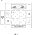
- FIG. 1 illustrates an exemplary neural network processing unit (NPU) architecture 100.
- NPU architecture 100 can include an on-chip communication system 110, an off-chip memory 120, a memory controller 130, a direct memory access (DMA) unit 140, a Joint Test Action Group (JTAG)/Test Access End (TAP) controller 150, a peripheral component interconnect express (PCIe) interface 160, inter-chip links 170, and the like.
- DMA direct memory access
- JTAG Joint Test Action Group
- TAP Test Access End
- PCIe peripheral component interconnect express
- On-chip communication system 110 can include a global manager 112 and a plurality of tiles 116.
- Global manager 112 can include one or more cluster managers 114 configured to coordinate with one or more tiles 116.
- Each cluster manager 114 can be associated with an array of tiles 116 that provide synapse/neuron circuitry for the neural network.
- the top layer of tiles of FIG. 1 may provide circuitry representing an input layer to neural network, while the second layer of tiles may provide circuitry representing a hidden layer of the neural network.
- global manager 112 can include two cluster managers 114 configured to coordinate with two arrays of tiles 116.
- Tiles 116 can include one or more multipliers, adders, multiply-accumulators (e.g., a set of multiply-accumulators of a SIMD architecture) and corresponding memory and can be configured to perform an operation (e.g., one or more algorithmic calculations) on the communicated data under the control of global manager 112.
- multiply-accumulators e.g., a set of multiply-accumulators of a SIMD architecture
- an operation e.g., one or more algorithmic calculations
- Off-chip memory 120 can include read-only memory (ROM), erasable programmable read-only memory (EPROM) or the like. Off-chip memory 120 can be configured to store a large amount of data with slower access speed, compared to the on-chip memory integrated within one or more processor.
- ROM read-only memory
- EPROM erasable programmable read-only memory
- Memory controller 130 can read, write, or refresh one or more memory devices.
- the memory devices can include on-chip memory and off-chip memory 120.
- the memory device can be implemented as any type of volatile or non-volatile memory devices, or a combination thereof, such as a static random access memory (SRAM), an electrically erasable programmable read-only memory (EEPROM), an erasable programmable read-only memory (EPROM), a programmable read-only memory (PROM), a read-only memory (ROM), a magnetic memory, a flash memory, or a magnetic or optical disk.
- SRAM static random access memory
- EEPROM electrically erasable programmable read-only memory
- EPROM erasable programmable read-only memory
- PROM programmable read-only memory
- ROM read-only memory
- magnetic memory a magnetic memory
- flash memory or a magnetic or optical disk.
- DMA unit 140 can generate memory addresses and initiate memory read or write cycles.
- DMA unit 140 can contain several hardware registers that can be written and read by the one or more processors.
- the registers can include a memory address register, a byte-count register, and one or more control registers. These registers can specify some combination of the source, the destination, the direction of the transfer (reading from the input/output (I/O) device or writing to the I/O device), the size of the transfer unit, and/or the number of bytes to transfer in one burst.
- JTAG/TAP controller 150 can specify a dedicated debug port implementing a serial communications interface (e.g., a JTAG interface) for low-overhead access without requiring direct external access to the system address and data buses.
- the JTAG/TAP controller 150 can also specify an on-chip test access interface (e.g., a TAP interface) that implements a protocol to access a set of test registers that present chip logic levels and device capabilities of various parts.
- Peripheral interface 160 can support full-duplex communication between any two endpoints, with no inherent limitation on concurrent access across multiple endpoints.
- Inter-chip links 170 can connect all the internal components of NPU architecture 100, such as on-chip communication system 110, off-chip memory 120, memory controller 130, DMA unit 140, JTAG/TAP controller 150, and PCIe interface 160 to each other.
- NPU architecture 100 incorporates the embodiments of the present disclosure, it is appreciated that the disclosed embodiments can be applied to chips with SIMD architecture for accelerating some applications such as deep learning.
- Such chips can be, for example, GPU, CPU with vector processing ability, or neural network accelerators for deep learning.
- SIMD or vector architecture is commonly used to support computing devices with data parallelism, such as graphics processing and deep learning.
- the SIMD architecture can include multiple processing elements, wherein each of the processing elements can perform the same operation on multiple data points simultaneously.
- the private memory can be memory dedicated to serving data for each single processing element among multiple parallel processing elements
- shared memory can refer to memory dedicated to serving data for all parallel processing elements.
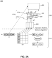
- FIG. 2A illustrates an exemplary functionality of a layer 200 of neural network, including a software algorithm 210 and hardware 220.
- Hardware 220 can include a private memory module 230, a processing unit array 240, a shared memory module 250, a write buffer 260, input operands 270, output operand 280, and the like.
- hardware 220 can be located in a tile (e.g., tile 116 of FIG. 1 ).
- a processing unit of processing unit array 240 can be an Arithmetic Logic Unit (ALU), a Floating Point Unit (FPU), a CPU, a GPU, or the like.
- An ALU is a fundamental building block of a computing circuit, including the CPU of computers.
- a single CPU can contain one or more ALUs.
- an ALU is a combinational digital electronic circuit that performs arithmetic and bitwise operations on integer binary numbers.
- Processing unit array 240 can include multiple processing units 242, 244, 246, and 248, for example, an array of processing units, as illustrated in FIG. 2B .
- Private memory module 230 can be partitioned into separate private memory blocks, such that, each of the multiple processing units 242, 244, 246, and 248 has a corresponding private memory block 232, 234, 236, and 238, as shown in FIG. 2B .
- Input operands 270 can be the input data operated on by processing unit array 240.
- input operands 270 of FIG. 2A can include one or more private input operand(s) 272 and one or more shared input operand(s) 274, as shown in FIG. 2B .
- Private input operand 272 can be stored in private memory module 230 and shared input operand 274 can be stored in shared memory module 250.
- software algorithms 210 have shared data that can be stored in shared memory module 250 and can be broadcasted to each of the multiple processing units 242, 244, 246, and 248 of processing unit array 240 as a shared operand 274.
- "b” can include a constant value
- X can include a shared input operand 274
- W 1 can include a private input operand 272.
- the vector size can be set as any natural number.
- a vector size of 4 is taken as an example, and a 4-way SIMD hardware to compute the vector is used.
- the shaded blocks and dotted lines in FIG. 2A indicate how "a1" is calculated. From this calculation, it is appreciated that data in each column of the "W1" array is local to a corresponding processing unit of processing unit array 240 and the data can accordingly be stored in corresponding memory block of private memory module 230, as a private input operand 272. For example, the data in each of the first, second, third, and fourth columns of the W1 array can be stored in their corresponding memory blocks 232, 234, 236, and 238 of private memory module 230 as private input operands.
- the W1 array can include a matrix of stored data, wherein each element of the matrix is represented as W1ij or W1_ ij (as shown later), where "i" represents the row number and "j" represents the column number in the matrix.
- W1 41 represents the data stored in the element located at row 4 and column 1 of the W1 array.
- Other commonly known notations to address elements in a matrix can be used as well.
- Equations 2-5 represent exemplary operations performed in layer 200 of a neural network processor, designed to calculate a1, a2, a3 and a4.
- machine learning or deep learning includes training the neural network processor to generate an end result based on input data, accomplished by implementing algorithms for one or more layers of neural processing.
- layer 200 of FIG. 2A represents a first layer including an algorithm configured to perform an operation using a bias b, data stored in the X array, and data stored in W1 array.
- a second and third layer (not shown) can include algorithms using the bias b, data stored in the X array, and data stored in W2 and W3 array.
- Each layer can include a different value of bias b and different parameters stored in "W" array.
- array X can include an individual's scores in different classes.
- the value of x1 of the array X can be student A's Math score
- x2 can be the English score
- x3 can be the History score
- x4 can be the Science score.
- the end result can be whether the individual will be granted admission in a school or rejected, based on the scores (input data).
- data x1-x4 is "shared" and common in calculating a1-a4.
- FIG. 3 illustrates data sharing in multi-layer networks.
- Data sharing refers to how previously private data can become shared data in a later phase of a program.
- neural network architecture 300 includes multiple layers, for example, layers 310 and 320.
- output operand 280 of layer 310 can be used as an input operand 270 for layer 320.
- the output operand 280 of one layer can be utilized as input operand 270 by one or more layers.
- a1 is calculated by processing unit 242 of private memory module 230.
- the data in a1 becomes a broadcasting input for layer 320.
- a neural network can be organized in layers. Each layer can perform one or more calculations on its inputs and generate an output.
- the output of a layer can be passed onto a next layer for further processing. For example, an output of a previous layer can be an input for the next layer. Accordingly, the locally generated "a"s have to be either stored back to shared memory 250, or stored to private memory 230 and copied later to shared memory 250.
- a write buffer 260 is introduced to allow shared memory 250 more time to consume these output operands 280 individually.
- the output speed of processing unit array 240 is faster than the width of write buffer 260, e.g., the size of A is greater than X, write buffer 260 may propagate a back pressure, forcing the processing unit array 240 to slow down, resulting in the slowdown of the overall program execution.
- FIG. 4A illustrates a schematic diagram of an exemplary hardware system 400 including unified organization of memory modules.
- Hardware system 400 includes a unified storage medium 405 and processing units 242, 244, 246, and 248.
- Unified storage medium 405 includes one or more storage modules 410, each including storage cells 430 configured to store input operand 270, output data 280. Multiple storage modules 410 can be merged into a single medium to form unified storage medium 405.
- Each storage module 410 can include a private storage module 412 and a shared storage module 414.
- Hardware system 400 can include multiple processing units 242, 244, 246, and 248.
- Each of the multiple processing units of the processing unit array 240 is configured to communicate with one or more storage modules.
- processing unit 242 can receive private input operand 272 from private storage module 412.
- Processing unit 242 can also receive shared input operand 274 from one or more shared storage modules 414.
- processing unit array 240 is configured to receive private input operand 272 from private storage module 412, receive shared input operand 274 from shared storage module 414, and generate an output operand 280 based on private input operand 272 and shared input operand 274.
- each of the storage cells 430 can be uniquely identified by a unique identifier 440.
- Unique identifier 440 can be a bit address including high-order bits 442 and low-order bits 444, or a byte address including high-order and low-order bytes, or a combination thereof.
- high-order bits 442 can be the most significant bit (MSB).
- MSB can also be referred to as the left-most bit due to the convention in positional notation of writing more significant digits further to the left.
- Low-order bits 444 are referred to as bits in the right-most position.
- the high-order bits 442 refer to the left-most bit, i.e. "2” and the low-order bits 444 refer to the bits on the right side, i.e. "E5".
- storage cell 430 is a private storage cell 432 or a shared storage cell 434.
- Private storage cells 432 can be located within private storage module 412.
- Shared storage cells 434 can be located within shared storage module 414.
- High-order bits 442 of unique identifier 440 are configured to indicate a target storage module for operand (270, 280) and low-order bits 444 of unique identifier 440 are configured to indicate a target storage cell within target storage module, for operand (270, 280).
- unique identifier 440 having a bit address "2_E5" refers to storage module "2", and storage cell "E5" within storage module "2".
- high-order bits 442 can also indicate the processing unit to which the storage module is "private" to, and low-order bits 444 indicate the location within the storage module.
- private storage cells 432 and shared storage cells 434 are physically indistinguishable storage cells and are not pre-labelled as such.
- the attribute of "private” and “shared” for a storage cell is determined based on the compiler-generated instructions programmed to address the data. For example, data can be stored in any cell.
- the compiler-generated instructions refer to the data as "private,” the data may be read out in parallel as private input operand 272.
- the compiler-generated instructions refer to the data as "shared”
- the data may be read out as shared input operand 274.
- unique identifier 440 includes other characters, for example, numeric characters, alpha-numeric characters, hexadecimal numerals (e.g., shown in FIG. 4A ), octal numerals, or the like, addressable by a software addressing mode.
- processing unit array 240 or each of the multiple processing units can generate output data 280.
- Output data 280 can be a private output data 282 or a shared output data 284, determined by the operations in the next layer of a multi-layered algorithm for a neural network processor. As illustrated in FIG. 4A , output data 280 can be considered private output data 282 since it is written back to unified storage medium in parallel in each of the storage modules 410.
- neural network processors comprise a compiler (not shown).
- the compiler is a program or computer software that transforms computer code written in one programming language into another programming language to create an executable program.
- a compiler can perform a variety of operations, for example, pre-processing, lexical analysis, parsing, semantic analysis, conversion of input programs to an intermediate representation, code optimization, and code generation, or combinations thereof.
- FIG. 5 is a process flowchart of an exemplary data organization operation 500, consistent with embodiments of the present disclosure.
- data organization operation 500 can be performed by an on-chip communication system (e.g., on-chip communication system 110).
- Step 502 includes configuring a storage module (e.g., storage module 410) of a unified storage medium (e.g., unified storage medium 400) to include multiple storage cells (e.g. storage cells 430).
- step 502 includes configuring a private storage module (e.g., private storage module 412) to include private storage cells (e.g., private storage cell 432) and/or a shared storage module 414 (e.g., shared storage module 414) to include shared storage cells (e.g., shared storage cell 434).
- Configuring a storage module to include storage cells can comprise allocating storage space based on the total storage space available, software programs or algorithms, hardware limitations, time restrictions, and the like. If a software application or an algorithm is multi-layered and requires multiple layers of computation including more shared data than private data, the storage module can be configured to comprise more shared storage cells or more shared storage modules.
- Step 504 includes configuring a storage medium (e.g., unified storage medium 400 of FIG. 4A ) to communicate with a processing unit (e.g., processing unit array 240) or multiple processing units.
- the processing unit is an Arithmetic Logic Unit (ALU), a Floating Point Unit (FPU), a Central Processing Unit (CPU), or a Graphics Processing Unit (GPU).
- a single CPU can contain one or more ALUs.
- an ALU is a combinational digital electronic circuit that performs arithmetic and bitwise operations on integer binary numbers.
- the processing unit can include multiple processing units, for example, an array of processing units configured to operate in parallel.
- Communicating with a processing unit can include receiving data generated by the processing unit, or providing stored data to the processing unit.
- the storage medium can be the source of data to be computed on or the target of data storage.
- the hardware system comprises a single processing unit configured to receive data from multiple storage modules.
- the hardware system can also include a unique processing unit for each storage module, configured to receive data only from the corresponding storage module.
- processing unit e.g., processing unit array 240
- output data e.g., output data 280
- the compiler may be a program or computer software that transforms computer code written in one programming language into another programming language to create an executable program.
- the compiler can generate a set of instructions configured to access data from a storage medium, execute a desired operation on the accessed data, generate output data based on the operation, and store the generated output data back into the storage medium for subsequent processing.
- the instructions can also include assigning a characteristic to the input and the output data. The characteristic of the data can be private, shared, restricted, or the like.
- the set of instructions will be described with reference to FIG. 4A , in accordance with embodiments of the disclosure.
- the instructions in the aforementioned set of instructions generally comprise an operation on the data, characteristic of the data, and a target location within the storage medium.
- operation on the data includes load (reading), store (writing), arithmetic operations, (e.g., addition, subtraction, multiplication, division) copy, paste, and the like.
- Characteristic of the data can refer generally to the accessibility of the data within the storage medium. Characteristic of the data can include private, shared, restricted, allowed, global, local, or combinations thereof.
- Data in general, is referred to as an operand. Data can be an input operand, for example, operand 1 (OP1) and operand 2 (OP2), or an output data based on the vector operation being performed.
- the subfield of load/store instructions implies how to load/store the data.
- Subfield ".SHARED” implies that the data should be read or written as shared data. In this mode, both high-order bits (e.g., 442 of FIG. 4B ) and low-order bits (e.g., 444 of FIG. 4B ) are utilized to determine the target location of input operand or output data.
- Subfield ".SIMD” implies that the data should be read or written as private data in parallel, wherein, the high-order bits can be disregarded by hardware and the low-order bits are utilized to determine the target location of input operand or output data.
- each processing unit e.g., 242, 244, 246, and 248 of FIG. 4A ) reads input operand 1 (e.g., private input operand 272) in parallel.
- the high-order bit "0" in bit address "0_00” is not utilized, and the low-order bits "00" indicate the storage cell and a characteristic of the storage cell. (e.g., private storage cell 432)
- all data in row 1 of the "W1" array (W1_ 1i ) is read out simultaneously but separately to each corresponding processing unit.
- the "LOAD.SIMD" field implies that the data should be read in parallel.
- input operand 2 (e.g., shared input operand 274) is read once and broadcast to all processing units, as illustrated in FIG. 4A .
- the high-order bit “0" in bit address "0_F0" indicates the storage module where the data is stored, and the low-order bits “F0” indicate the storage cell and a characteristic of the storage cell in which the data is stored (e.g., shared storage cell 434).
- the data in "X1" of the "X" array is read out read once and broadcast to each corresponding processing unit.
- the LOAD.SHARED field implies that the data should be read as shared data between all processing units.
- processing unit performs multiplication of input operands 1 and 2, as defined by the vector operation, to generate an output data "A".
- the arithmetic operation can include basic arithmetic functions of addition, subtraction, multiplication, or division, or combinations thereof.
- processing unit is configured to perform complex arithmetic and algebraic functions, logarithmic functions, exponentiation, or the like.
- generated output data "A” in instruction i3 is stored in parallel back to storage medium for further processing.
- Generated output data "A” (e.g., output data 280) can be used as the input operand in the next layer of the multi-layered algorithm.
- the high-order bit “0" in bit address "0_F1” is not utilized by hardware, and the low-order bits "F1" indicate the storage cell and a characteristic of the storage cell (e.g., shared storage cell 434) for the output data to be stored.
- output data 280 may be temporarily stored in a temporary storage (e.g., write buffer 260) before storing it in the shared or private storage module of the unified storage medium.
- step 508 generated output data is stored back in the unified storage medium for further processing.
- a neural network can be organized in multiple layers.
- the output of a layer can be passed onto a next layer for further processing.
- an output of a previous layer can be an input for the next layer.
Landscapes
- Engineering & Computer Science (AREA)
- Theoretical Computer Science (AREA)
- Physics & Mathematics (AREA)
- General Engineering & Computer Science (AREA)
- General Physics & Mathematics (AREA)
- Health & Medical Sciences (AREA)
- Life Sciences & Earth Sciences (AREA)
- Biomedical Technology (AREA)
- Biophysics (AREA)
- Mathematical Physics (AREA)
- Software Systems (AREA)
- Molecular Biology (AREA)
- General Health & Medical Sciences (AREA)
- Neurology (AREA)
- Data Mining & Analysis (AREA)
- Evolutionary Computation (AREA)
- Computational Linguistics (AREA)
- Computing Systems (AREA)
- Artificial Intelligence (AREA)
- Computer Hardware Design (AREA)
- Memory System (AREA)
- Multi Processors (AREA)
- Information Retrieval, Db Structures And Fs Structures Therefor (AREA)
Applications Claiming Priority (3)
| Application Number | Priority Date | Filing Date | Title |
|---|---|---|---|
| US201762610119P | 2017-12-22 | 2017-12-22 | |
| US15/984,255 US11436143B2 (en) | 2017-12-22 | 2018-05-18 | Unified memory organization for neural network processors |
| PCT/US2018/067301 WO2019126758A1 (en) | 2017-12-22 | 2018-12-21 | A unified memory organization for neural network processors |
Publications (3)
| Publication Number | Publication Date |
|---|---|
| EP3729279A1 EP3729279A1 (en) | 2020-10-28 |
| EP3729279A4 EP3729279A4 (en) | 2021-03-03 |
| EP3729279B1 true EP3729279B1 (en) | 2025-05-21 |
Family
ID=66949585
Family Applications (1)
| Application Number | Title | Priority Date | Filing Date |
|---|---|---|---|
| EP18890583.0A Active EP3729279B1 (en) | 2017-12-22 | 2018-12-21 | A unified memory organization for neural network processors |
Country Status (5)
| Country | Link |
|---|---|
| US (1) | US11436143B2 (enExample) |
| EP (1) | EP3729279B1 (enExample) |
| JP (1) | JP7266602B2 (enExample) |
| CN (1) | CN111630502B (enExample) |
| WO (1) | WO2019126758A1 (enExample) |
Families Citing this family (17)
| Publication number | Priority date | Publication date | Assignee | Title |
|---|---|---|---|---|
| US11586910B1 (en) * | 2018-04-20 | 2023-02-21 | Perceive Corporation | Write cache for neural network inference circuit |
| US11481612B1 (en) | 2018-04-20 | 2022-10-25 | Perceive Corporation | Storage of input values across multiple cores of neural network inference circuit |
| US12093696B1 (en) | 2018-04-20 | 2024-09-17 | Perceive Corporation | Bus for transporting output values of a neural network layer to cores specified by configuration data |
| US11783167B1 (en) | 2018-04-20 | 2023-10-10 | Perceive Corporation | Data transfer for non-dot product computations on neural network inference circuit |
| US10740434B1 (en) | 2018-04-20 | 2020-08-11 | Perceive Corporation | Reduced dot product computation circuit |
| US11568227B1 (en) | 2018-04-20 | 2023-01-31 | Perceive Corporation | Neural network inference circuit read controller with multiple operational modes |
| US11295200B1 (en) | 2018-04-20 | 2022-04-05 | Perceive Corporation | Time-multiplexed dot products for neural network inference circuit |
| US11461623B2 (en) * | 2018-10-18 | 2022-10-04 | Taiwan Semiconductor Manufacturing Co., Ltd. | Method and apparatus for defect-tolerant memory-based artificial neural network |
| US11995533B1 (en) | 2018-12-05 | 2024-05-28 | Perceive Corporation | Executing replicated neural network layers on inference circuit |
| FR3089649A1 (fr) * | 2018-12-06 | 2020-06-12 | Stmicroelectronics (Rousset) Sas | Procédé et dispositif de détermination de la taille mémoire globale d’une zone mémoire globale allouée aux données d’un réseau de neurones |
| FR3094104A1 (fr) | 2019-03-20 | 2020-09-25 | Stmicroelectronics (Rousset) Sas | Procédé et dispositif de détermination de la taille mémoire globale d’une zone mémoire globale allouée aux données d’un réseau de neurones compte tenu de sa topologie |
| US11615322B1 (en) | 2019-05-21 | 2023-03-28 | Perceive Corporation | Compiler for implementing memory shutdown for neural network implementation configuration |
| CN113204478B (zh) * | 2021-04-06 | 2022-05-03 | 北京百度网讯科技有限公司 | 测试单元的运行方法、装置、设备和存储介质 |
| US12159214B1 (en) | 2021-04-23 | 2024-12-03 | Perceive Corporation | Buffering of neural network inputs and outputs |
| KR20230168574A (ko) | 2022-06-07 | 2023-12-14 | 리벨리온 주식회사 | 뉴럴 프로세싱 장치의 공유 페이지 테이블 사용 방법 및 피지컬 페이지 할당 방법 |
| KR102509472B1 (ko) * | 2022-06-07 | 2023-03-14 | 리벨리온 주식회사 | 뉴럴 프로세싱 장치 및 그의 공유 페이지 테이블 사용 방법 |
| KR102774907B1 (ko) * | 2022-12-14 | 2025-03-04 | 리벨리온 주식회사 | 뉴럴 프로세서 |
Citations (2)
| Publication number | Priority date | Publication date | Assignee | Title |
|---|---|---|---|---|
| US20160232107A1 (en) * | 2015-02-05 | 2016-08-11 | Alberto Ros | Systems and methods for coherence in clustered cache hierarchies |
| GB2543520A (en) * | 2015-10-20 | 2017-04-26 | Advanced Risc Mach Ltd | Memory access instructions |
Family Cites Families (20)
| Publication number | Priority date | Publication date | Assignee | Title |
|---|---|---|---|---|
| JPH02292684A (ja) * | 1989-05-06 | 1990-12-04 | Takayama:Kk | 画像認識システム |
| US5956703A (en) * | 1995-07-28 | 1999-09-21 | Delco Electronics Corporation | Configurable neural network integrated circuit |
| JP2001290699A (ja) * | 2000-04-10 | 2001-10-19 | Matsushita Electric Ind Co Ltd | デュアルポートramアクセス装置 |
| US7073044B2 (en) * | 2001-03-30 | 2006-07-04 | Intel Corporation | Method and apparatus for sharing TLB entries |
| GB2419005B (en) | 2002-04-22 | 2006-06-07 | Micron Technology Inc | Providing a register file memory with local addressing in a SIMD parallel processor |
| GB2417105B (en) | 2004-08-13 | 2008-04-09 | Clearspeed Technology Plc | Processor memory system |
| GB0623276D0 (en) * | 2006-11-22 | 2007-01-03 | Transitive Ltd | Memory consistency protection in a multiprocessor computing system |
| US8271763B2 (en) | 2009-09-25 | 2012-09-18 | Nvidia Corporation | Unified addressing and instructions for accessing parallel memory spaces |
| US8990506B2 (en) * | 2009-12-16 | 2015-03-24 | Intel Corporation | Replacing cache lines in a cache memory based at least in part on cache coherency state information |
| US8868848B2 (en) * | 2009-12-21 | 2014-10-21 | Intel Corporation | Sharing virtual memory-based multi-version data between the heterogenous processors of a computer platform |
| US8982140B2 (en) * | 2010-09-24 | 2015-03-17 | Nvidia Corporation | Hierarchical memory addressing |
| US9274960B2 (en) * | 2012-03-20 | 2016-03-01 | Stefanos Kaxiras | System and method for simplifying cache coherence using multiple write policies |
| US9009419B2 (en) * | 2012-07-31 | 2015-04-14 | Advanced Micro Devices, Inc. | Shared memory space in a unified memory model |
| WO2014031540A1 (en) * | 2012-08-20 | 2014-02-27 | Cameron Donald Kevin | Processing resource allocation |
| US9563425B2 (en) * | 2012-11-28 | 2017-02-07 | Intel Corporation | Instruction and logic to provide pushing buffer copy and store functionality |
| US9733995B2 (en) * | 2014-12-17 | 2017-08-15 | Intel Corporation | Scalable synchronization mechanism for distributed memory |
| EP3035204B1 (en) | 2014-12-19 | 2018-08-15 | Intel Corporation | Storage device and method for performing convolution operations |
| US9940287B2 (en) * | 2015-03-27 | 2018-04-10 | Intel Corporation | Pooled memory address translation |
| US10664751B2 (en) * | 2016-12-01 | 2020-05-26 | Via Alliance Semiconductor Co., Ltd. | Processor with memory array operable as either cache memory or neural network unit memory |
| US20170060736A1 (en) * | 2015-12-09 | 2017-03-02 | Mediatek Inc. | Dynamic Memory Sharing |
-
2018
- 2018-05-18 US US15/984,255 patent/US11436143B2/en active Active
- 2018-12-21 JP JP2020532976A patent/JP7266602B2/ja active Active
- 2018-12-21 WO PCT/US2018/067301 patent/WO2019126758A1/en not_active Ceased
- 2018-12-21 EP EP18890583.0A patent/EP3729279B1/en active Active
- 2018-12-21 CN CN201880074349.6A patent/CN111630502B/zh active Active
Patent Citations (2)
| Publication number | Priority date | Publication date | Assignee | Title |
|---|---|---|---|---|
| US20160232107A1 (en) * | 2015-02-05 | 2016-08-11 | Alberto Ros | Systems and methods for coherence in clustered cache hierarchies |
| GB2543520A (en) * | 2015-10-20 | 2017-04-26 | Advanced Risc Mach Ltd | Memory access instructions |
Also Published As
| Publication number | Publication date |
|---|---|
| EP3729279A1 (en) | 2020-10-28 |
| US20190196970A1 (en) | 2019-06-27 |
| EP3729279A4 (en) | 2021-03-03 |
| WO2019126758A1 (en) | 2019-06-27 |
| CN111630502A (zh) | 2020-09-04 |
| JP7266602B2 (ja) | 2023-04-28 |
| CN111630502B (zh) | 2024-04-16 |
| US11436143B2 (en) | 2022-09-06 |
| JP2021507383A (ja) | 2021-02-22 |
Similar Documents
| Publication | Publication Date | Title |
|---|---|---|
| EP3729279B1 (en) | A unified memory organization for neural network processors | |
| US11714780B2 (en) | Compiler flow logic for reconfigurable architectures | |
| CN111630505B (zh) | 深度学习加速器系统及其方法 | |
| JP7264897B2 (ja) | メモリ装置及びそれを制御するための方法 | |
| US11921814B2 (en) | Method and device for matrix multiplication optimization using vector registers | |
| US20190130270A1 (en) | Tensor manipulation within a reconfigurable fabric using pointers | |
| CN114341805A (zh) | 纯函数语言神经网络加速器系统及结构 | |
| US10970043B2 (en) | Programmable multiply-add array hardware | |
| US11544189B2 (en) | System and method for memory management | |
| US7573481B2 (en) | Method and apparatus for management of bit plane resources | |
| US10915317B2 (en) | Multiple-pipeline architecture with special number detection |
Legal Events
| Date | Code | Title | Description |
|---|---|---|---|
| STAA | Information on the status of an ep patent application or granted ep patent |
Free format text: STATUS: THE INTERNATIONAL PUBLICATION HAS BEEN MADE |
|
| PUAI | Public reference made under article 153(3) epc to a published international application that has entered the european phase |
Free format text: ORIGINAL CODE: 0009012 |
|
| STAA | Information on the status of an ep patent application or granted ep patent |
Free format text: STATUS: REQUEST FOR EXAMINATION WAS MADE |
|
| 17P | Request for examination filed |
Effective date: 20200717 |
|
| AK | Designated contracting states |
Kind code of ref document: A1 Designated state(s): AL AT BE BG CH CY CZ DE DK EE ES FI FR GB GR HR HU IE IS IT LI LT LU LV MC MK MT NL NO PL PT RO RS SE SI SK SM TR |
|
| AX | Request for extension of the european patent |
Extension state: BA ME |
|
| A4 | Supplementary search report drawn up and despatched |
Effective date: 20210201 |
|
| RIC1 | Information provided on ipc code assigned before grant |
Ipc: G06N 3/063 20060101ALI20210126BHEP Ipc: G06F 12/02 20060101ALI20210126BHEP Ipc: G06F 9/30 20180101ALI20210126BHEP Ipc: G06F 12/06 20060101ALI20210126BHEP Ipc: G11C 11/54 20060101ALI20210126BHEP Ipc: G06F 13/00 20060101AFI20210126BHEP |
|
| DAV | Request for validation of the european patent (deleted) | ||
| DAX | Request for extension of the european patent (deleted) | ||
| STAA | Information on the status of an ep patent application or granted ep patent |
Free format text: STATUS: EXAMINATION IS IN PROGRESS |
|
| 17Q | First examination report despatched |
Effective date: 20230130 |
|
| P01 | Opt-out of the competence of the unified patent court (upc) registered |
Effective date: 20230418 |
|
| RAP1 | Party data changed (applicant data changed or rights of an application transferred) |
Owner name: T-HEAD (SHANGHAI) SEMICONDUCTOR CO., LTD. |
|
| GRAP | Despatch of communication of intention to grant a patent |
Free format text: ORIGINAL CODE: EPIDOSNIGR1 |
|
| STAA | Information on the status of an ep patent application or granted ep patent |
Free format text: STATUS: GRANT OF PATENT IS INTENDED |
|
| INTG | Intention to grant announced |
Effective date: 20241212 |
|
| GRAS | Grant fee paid |
Free format text: ORIGINAL CODE: EPIDOSNIGR3 |
|
| GRAA | (expected) grant |
Free format text: ORIGINAL CODE: 0009210 |
|
| STAA | Information on the status of an ep patent application or granted ep patent |
Free format text: STATUS: THE PATENT HAS BEEN GRANTED |
|
| AK | Designated contracting states |
Kind code of ref document: B1 Designated state(s): AL AT BE BG CH CY CZ DE DK EE ES FI FR GB GR HR HU IE IS IT LI LT LU LV MC MK MT NL NO PL PT RO RS SE SI SK SM TR |
|
| REG | Reference to a national code |
Ref country code: GB Ref legal event code: FG4D |
|
| REG | Reference to a national code |
Ref country code: CH Ref legal event code: EP |
|
| REG | Reference to a national code |
Ref country code: DE Ref legal event code: R096 Ref document number: 602018082199 Country of ref document: DE |
|
| REG | Reference to a national code |
Ref country code: IE Ref legal event code: FG4D |
|
| REG | Reference to a national code |
Ref country code: NL Ref legal event code: MP Effective date: 20250521 |
|
| PG25 | Lapsed in a contracting state [announced via postgrant information from national office to epo] |
Ref country code: FI Free format text: LAPSE BECAUSE OF FAILURE TO SUBMIT A TRANSLATION OF THE DESCRIPTION OR TO PAY THE FEE WITHIN THE PRESCRIBED TIME-LIMIT Effective date: 20250521 Ref country code: ES Free format text: LAPSE BECAUSE OF FAILURE TO SUBMIT A TRANSLATION OF THE DESCRIPTION OR TO PAY THE FEE WITHIN THE PRESCRIBED TIME-LIMIT Effective date: 20250521 Ref country code: PT Free format text: LAPSE BECAUSE OF FAILURE TO SUBMIT A TRANSLATION OF THE DESCRIPTION OR TO PAY THE FEE WITHIN THE PRESCRIBED TIME-LIMIT Effective date: 20250922 |
|
| REG | Reference to a national code |
Ref country code: LT Ref legal event code: MG9D |
|
| PG25 | Lapsed in a contracting state [announced via postgrant information from national office to epo] |
Ref country code: NO Free format text: LAPSE BECAUSE OF FAILURE TO SUBMIT A TRANSLATION OF THE DESCRIPTION OR TO PAY THE FEE WITHIN THE PRESCRIBED TIME-LIMIT Effective date: 20250821 Ref country code: GR Free format text: LAPSE BECAUSE OF FAILURE TO SUBMIT A TRANSLATION OF THE DESCRIPTION OR TO PAY THE FEE WITHIN THE PRESCRIBED TIME-LIMIT Effective date: 20250822 |
|
| PG25 | Lapsed in a contracting state [announced via postgrant information from national office to epo] |
Ref country code: NL Free format text: LAPSE BECAUSE OF FAILURE TO SUBMIT A TRANSLATION OF THE DESCRIPTION OR TO PAY THE FEE WITHIN THE PRESCRIBED TIME-LIMIT Effective date: 20250521 Ref country code: PL Free format text: LAPSE BECAUSE OF FAILURE TO SUBMIT A TRANSLATION OF THE DESCRIPTION OR TO PAY THE FEE WITHIN THE PRESCRIBED TIME-LIMIT Effective date: 20250521 |
|
| PG25 | Lapsed in a contracting state [announced via postgrant information from national office to epo] |
Ref country code: BG Free format text: LAPSE BECAUSE OF FAILURE TO SUBMIT A TRANSLATION OF THE DESCRIPTION OR TO PAY THE FEE WITHIN THE PRESCRIBED TIME-LIMIT Effective date: 20250521 |
|
| PG25 | Lapsed in a contracting state [announced via postgrant information from national office to epo] |
Ref country code: HR Free format text: LAPSE BECAUSE OF FAILURE TO SUBMIT A TRANSLATION OF THE DESCRIPTION OR TO PAY THE FEE WITHIN THE PRESCRIBED TIME-LIMIT Effective date: 20250521 |
|
| PG25 | Lapsed in a contracting state [announced via postgrant information from national office to epo] |
Ref country code: RS Free format text: LAPSE BECAUSE OF FAILURE TO SUBMIT A TRANSLATION OF THE DESCRIPTION OR TO PAY THE FEE WITHIN THE PRESCRIBED TIME-LIMIT Effective date: 20250821 |
|
| PG25 | Lapsed in a contracting state [announced via postgrant information from national office to epo] |
Ref country code: IS Free format text: LAPSE BECAUSE OF FAILURE TO SUBMIT A TRANSLATION OF THE DESCRIPTION OR TO PAY THE FEE WITHIN THE PRESCRIBED TIME-LIMIT Effective date: 20250921 |
|
| PG25 | Lapsed in a contracting state [announced via postgrant information from national office to epo] |
Ref country code: LV Free format text: LAPSE BECAUSE OF FAILURE TO SUBMIT A TRANSLATION OF THE DESCRIPTION OR TO PAY THE FEE WITHIN THE PRESCRIBED TIME-LIMIT Effective date: 20250521 |
|
| REG | Reference to a national code |
Ref country code: AT Ref legal event code: MK05 Ref document number: 1797357 Country of ref document: AT Kind code of ref document: T Effective date: 20250521 |