EP3729068B1 - Verfahren zur herstellung einer fluidsensorvorrichtung und fluidsensorvorrichtung - Google Patents
Verfahren zur herstellung einer fluidsensorvorrichtung und fluidsensorvorrichtung Download PDFInfo
- Publication number
- EP3729068B1 EP3729068B1 EP18836232.1A EP18836232A EP3729068B1 EP 3729068 B1 EP3729068 B1 EP 3729068B1 EP 18836232 A EP18836232 A EP 18836232A EP 3729068 B1 EP3729068 B1 EP 3729068B1
- Authority
- EP
- European Patent Office
- Prior art keywords
- arrangement
- fin
- fet
- layer
- contact
- Prior art date
- Legal status (The legal status is an assumption and is not a legal conclusion. Google has not performed a legal analysis and makes no representation as to the accuracy of the status listed.)
- Active
Links
Images


Classifications
-
- G—PHYSICS
- G01—MEASURING; TESTING
- G01N—INVESTIGATING OR ANALYSING MATERIALS BY DETERMINING THEIR CHEMICAL OR PHYSICAL PROPERTIES
- G01N27/00—Investigating or analysing materials by the use of electric, electrochemical, or magnetic means
- G01N27/26—Investigating or analysing materials by the use of electric, electrochemical, or magnetic means by investigating electrochemical variables; by using electrolysis or electrophoresis
- G01N27/403—Cells and electrode assemblies
- G01N27/414—Ion-sensitive or chemical field-effect transistors, i.e. ISFETS or CHEMFETS
- G01N27/4145—Ion-sensitive or chemical field-effect transistors, i.e. ISFETS or CHEMFETS specially adapted for biomolecules, e.g. gate electrode with immobilised receptors
-
- H—ELECTRICITY
- H10—SEMICONDUCTOR DEVICES; ELECTRIC SOLID-STATE DEVICES NOT OTHERWISE PROVIDED FOR
- H10P—GENERIC PROCESSES OR APPARATUS FOR THE MANUFACTURE OR TREATMENT OF DEVICES COVERED BY CLASS H10
- H10P90/00—Preparation of wafers not covered by a single main group of this subclass, e.g. wafer reinforcement
- H10P90/19—Preparing inhomogeneous wafers
- H10P90/1904—Preparing vertically inhomogeneous wafers
- H10P90/1906—Preparing SOI wafers
- H10P90/1914—Preparing SOI wafers using bonding
-
- G—PHYSICS
- G01—MEASURING; TESTING
- G01N—INVESTIGATING OR ANALYSING MATERIALS BY DETERMINING THEIR CHEMICAL OR PHYSICAL PROPERTIES
- G01N27/00—Investigating or analysing materials by the use of electric, electrochemical, or magnetic means
- G01N27/26—Investigating or analysing materials by the use of electric, electrochemical, or magnetic means by investigating electrochemical variables; by using electrolysis or electrophoresis
- G01N27/403—Cells and electrode assemblies
- G01N27/414—Ion-sensitive or chemical field-effect transistors, i.e. ISFETS or CHEMFETS
- G01N27/4146—Ion-sensitive or chemical field-effect transistors, i.e. ISFETS or CHEMFETS involving nanosized elements, e.g. nanotubes, nanowires
-
- G—PHYSICS
- G01—MEASURING; TESTING
- G01N—INVESTIGATING OR ANALYSING MATERIALS BY DETERMINING THEIR CHEMICAL OR PHYSICAL PROPERTIES
- G01N27/00—Investigating or analysing materials by the use of electric, electrochemical, or magnetic means
- G01N27/26—Investigating or analysing materials by the use of electric, electrochemical, or magnetic means by investigating electrochemical variables; by using electrolysis or electrophoresis
- G01N27/403—Cells and electrode assemblies
- G01N27/414—Ion-sensitive or chemical field-effect transistors, i.e. ISFETS or CHEMFETS
- G01N27/4148—Integrated circuits therefor, e.g. fabricated by CMOS processing
-
- H—ELECTRICITY
- H10—SEMICONDUCTOR DEVICES; ELECTRIC SOLID-STATE DEVICES NOT OTHERWISE PROVIDED FOR
- H10W—GENERIC PACKAGES, INTERCONNECTIONS, CONNECTORS OR OTHER CONSTRUCTIONAL DETAILS OF DEVICES COVERED BY CLASS H10
- H10W10/00—Isolation regions in semiconductor bodies between components of integrated devices
- H10W10/10—Isolation regions comprising dielectric materials
- H10W10/181—Semiconductor-on-insulator [SOI] isolation regions, e.g. buried oxide regions of SOI wafers
Definitions
- the present inventive concept generally relates to the field of semiconductor device fabrication, and in particular to a method for manufacturing a fluid sensor device and a fluid sensor device.
- FET field-effect transistors
- US 2012/0161333 A1 discloses a device for connecting nano-objects to external electrical systems, and method for producing the device.
- US 2015/0268189 A1 discloses a method of producing a FinFET sensor device.
- a method for manufacturing a fluid sensor device the method being defined by claim 1.
- the present inventive concept makes use of a fin-FET arrangement which is stacked on a CMOS arrangement.
- the fin-FET arrangement may provide a function as a fluid sensitive fin-FET arrangement.
- a stacked configuration may be formed, which allows forming of a very compact fluid sensor device.
- the CMOS arrangement may provide additional functionality to the fin-FET arrangement, e.g. the CMOS arrangement may comprise signal processing functionality to a signal acquired by the fin-FET arrangement.
- the CMOS arrangement may provide an amplifying structure configured to amplify a signal from the fin-FET arrangement.
- a fluid sensor device having a small surface area footprint may be provided.
- a fluid sensor device for single molecule detection may be realized. This may be especially useful for providing a dense arrangement of adjacent fin-FET arrangements, since signal processing circuitry for each fin-FET arrangement may be provided below the fin-FET arrangements rather than between the fin-FET arrangements.
- fluid sensitive fin-FET arrangement is to be understood as a fin-FET arrangement sensor sensitive to molecules, substances, or more generally an analyte in a fluid.
- the dielectric layers referred to in the present disclosure may comprise an oxide and/or any other dielectric material such as SiOC, SiN etc.
- a component such as a layer, a film, a region, or a plate
- the component may be directly on the other component or intervening components may be present thereon.
- the microfluidic structure need not necessarily be bonded to the third dielectric layer, but in contrast to any layer suitable for bonding to the microfluidic structure.
- the metallization layer referred to in the present disclosure may refer to a back end of line layer.
- the CMOS arrangement may comprise several metallization layers.
- the CMOS arrangement may comprise an amplifying structure configured to amplify a signal from the fin-FET arrangement.
- the amplifying structure may be a trans-impedance amplifier.
- the amplifying structure may be configured to convert a current signal into a voltage signal.
- the metallization layer may be configured to provide contact to the amplifying structure of the CMOS arrangement.
- the fin-FET arrangement may be in communicative contact with the amplifying structure of the CMOS arrangement.
- the method may further comprise forming a second dielectric layer over the fin-FET arrangement, and wherein the contact to the metallization layer and the fin-FET arrangement is configured to be at least partially enclosed by the planarized dielectric layer and the second dielectric layer.
- a contact comprising a first vertical portion configured to be in contact with the fin-FET arrangement, a second vertical portion configured to be in contact with the metallization layer, and a horizontal interconnecting structure configured to interconnect the metallization layer and the fin FET arrangement, may be achieved.
- the method may further comprise forming a third dielectric layer over the contact and the fin-FET arrangement.
- the second and third dielectric layer may form part of the channel.
- the channel may be a microfluidic channel.
- a channel comprising a sample chamber may be formed.
- the sample chamber may provide an increased volume for the fluid comprising the analyte.
- the two layers need not necessarily be separate dielectric layers.
- the second and third dielectric layer may be formed in a single step.
- a sample chamber providing an increased volume for the fluid comprising the analyte may be provided in other ways, e.g. by the microfluidic structure referred to in the following paragraph.
- the step of forming the channel may comprise removing a portion of the second and third dielectric layer, and bonding a microfluidic arrangement to the third dielectric layer.
- the bonding may be a fusion bonding.
- the microfluidic arrangement may provide additional microfluidic structures which may not be possible or preferable to form e.g. over the fin-FET arrangement.
- the microfluidic arrangement may comprise at least part of the inlet and outlet of the channel. It is to be understood that the microfluidic structure need not necessarily be bonded to the third dielectric layer, instead the microfluidic arrangement may be bonded to any layer capable of forming a bond with the microfluidic arrangement.
- the step of forming the channel may comprise removing a portion of the second dielectric layer, in case the third dielectric layer is not present.
- the contact may comprise a vertical arrangement comprising a first vertical portion configured to be in contact with the fin FET-arrangement, and a second vertical portion configured to be in contact with the metallization layer, wherein the interconnecting structure is configured to connect the metallization layer and the fin-FET arrangement via the vertical arrangement.
- the vertical arrangement may comprise tungsten.
- the interconnecting structure may comprise aluminum.
- the method may further comprise forming an etch stop layer over the fin-FET arrangement prior to the step of forming the contact to the metallization layer and the fin-FET arrangement.
- the etch stop layer may act as a protective layer for the fin-FET arrangement.
- the etch stop layer may facilitate the forming of the channel.
- the etch stop layer may comprise a material selected from the group consisting of SiN, metal oxides, and metal.
- the etch stop layer may be at least partially removed in conjunction with forming the channel, and a metal oxide layer may thereafter be formed over the fin-FET arrangement. This may be advantageous in case the etch stop layer is damaged or of poor quality due to the forming of the channel.
- the etch stop layer may be completely removed before forming the metal oxide layer over the fin-FET arrangement. In such case, the etch stop layer may be formed in any type of material suitable to act as an etch stop, as the etch stop layer is anyway completely removed later.
- the metal oxide layer may comprise AIO, HfO, SiO or similar materials.
- the metal oxide layer may provide a gate dielectric on the fin-FET arrangement.
- a portion of the interconnecting structure may be exposed in order to form a bond pad opening.
- the fluid sensor device may be connected to other devices.
- the step of forming a fin-FET arrangement in the silicon layer may be performed after the step of bonding the silicon-on-insulator arrangement to the CMOS arrangement, and after the step of removing the buried oxide and the silicon wafer.
- the removing of the buried oxide and the silicon wafer may not risk affecting a structure of the finFET arrangement.
- the forming of the fin-FET arrangement may be performed prior to the fin-FET arrangement being bonded to the CMOS arrangement.
- a thin film transfer process may be used, wherein a fin-FET arrangement formed on the silicon-on-insulator arrangement is transferred via the temporary carrier to be bonded to the CMOS arrangement.
- the method of the second aspect provides a fin-FET arrangement which is stacked on a CMOS arrangement.
- the fin-FET arrangement may provide a function as a fluid sensitive fin-FET arrangement.
- a stacked configuration may be formed, which allows forming of a very compact fluid sensor device.
- the step of forming a fin-FET arrangement in the silicon layer may be performed prior to the step of bonding the fin-FET arrangement to the CMOS arrangement.
- This order of processing may be advantageous when forming a fin-FET arrangement comprising at least one nanopore fin-FET.
- the CMOS arrangement is not affected by the procedure or procedures used to form the fin-FET arrangement.
- a higher resolution of the fin-FET arrangement may be achieved.
- higher temperatures are possible to be used in the forming of the finFET arrangement without risking damage to the CMOS arrangement.
- structures in relation to the fin-FET arrangement may be formed on the silicon-on-insulator arrangement before the fin-FET arrangement is transferred to be bonded to the CMOS arrangement.
- the fin-FET arrangement may be prepared with structures facing away from the CMOS arrangement, since such structures may be arranged above the fin-FET arrangement on the silicon-on-insulator arrangement and may be transferred to be bonded to the CMOS arrangement facing away from the CMOS arrangement.
- the fin-FET arrangement on the silicon-on-insulator arrangement may further be provided with a planarized dielectric layer for facilitating bonding to the temporary carrier.
- the fin-FET arrangement may for instance prior to bonding of the silicon-on-insulator arrangement to the temporary carrier be provided with a pre-metal dielectric layer through which connections e.g. to gates, source and drain areas in the fin-FET arrangement may be formed.
- the bonding of the fin-FET arrangement on the temporary carrier to the CMOS arrangement may be performed using the oxide of the buried oxide layer of the silicon-on-insulator arrangement.
- the buried oxide may be substantially removed in order to maintain a layer of the buried oxide to enable bonding to the CMOS arrangement.
- the entire buried oxide may be maintained and used in bonding to the CMOS arrangement.
- the buried oxide may be completely removed and another dielectric layer may be arranged on the temporary carrier for enabling bonding of the temporary carrier to the CMOS arrangement.
- CMOS arrangement is equally applicable to the method of the second aspect.
- features described above in relation to the contact to interconnect the metallization layer and the fin-FET arrangement are equally applicable to the method of the second aspect.
- features described above in relation to forming the channel are equally applicable to the method of the second aspect.
- the fin-FET arrangement may comprise nanopore fin-FETs. It is to be understood that the fin-FET arrangement may comprise at least one nanopore fin-FET.
- the nanopore fin-FETs may provide for that a fluid sensor device having a high sensitivity for molecule detection is achieved.
- nanopore fin-FET The operating principle of a nanopore fin-FET may be essentially the same as a traditional fin-FET.
- a fin-FET arrangement comprising at least one nanopore fin-FET may be achieved by forming and patterning a sacrificial layer, which when removed leaves a small pore, e.g. a nanopore.
- Other techniques may also be used to form a nanopore, such as ion/electron-beam sculpturing. It may be noted that different arrangements of nanopores are envisioned, such as arrays of nanopores enabling parallel sensing at high speed.
- the nanopore may advantageously be arranged in a gate area of a fin-FET structure or in a gate area of a structure corresponding to a fin-FET structure.
- An analyte passing the pore may modulate the source-drain current of the nanopore fin-FET, thus giving rise to a signal in the fluid sensor device.
- the nanopore of a nanopore fin-FET may have a diemeter of less than 10 nm, such as less than 5 nm.
- the method according to the second aspect may be particularly suitable for forming of a fin-FET arrangement comprising nanopore fin-FETs.
- a fluid sensor device comprising the features of claim 13.
- the fluid sensor device may provide a sensor equipment for analyzing an analyte in a fluid.
- the analyte may be any substance in a fluid, such as a biological substance, e.g. a DNA or RNA string, or any other substance, compound, or single molecule.
- the fin-FET arrangement utilizes the fact that an analyte contacting the fin-FET arrangement may change a charge of a gate of the fin-FET arrangement such that a conductance in the fin-FET arrangement is changed. This may cause a current to flow from source to drain in a transistor of the fin-FET arrangement such that a fluid sensor signal may be generated.
- the fluid sensor signal may be transferred to the CMOS arrangement for further processing, such as amplifying of the fluid sensor signal. Thanks to the fin-FET arrangement being arranged over the CMOS arrangement, a fluid sensor device having a small surface area footprint may be provided.
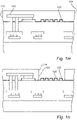
- FIGS. 1a - 1r illustrate steps which may form part of a method for manufacturing a fluid sensor device.
- some parts of the processes in the present disclosure may be omitted for the sake of brevity.
- some steps of masking, patterning, or etching may be omitted since it is believed that the person skilled in the art understands from the present disclosure as a whole how these steps are to be carried out within the present inventive concept.
- the illustrations are schematic and not to scale. In particular, the thickness of some layers have been exaggerated in order to more clearly illustrate the composition of the fluid sensor device.
- a method according to a first embodiment will be mainly described. However, as will be further discussed below, many of the steps illustrated for the method according to the first embodiment may also apply to a method according to a second emboiment. Therefore, the method according to the second embodiment will mainly be described in relation to steps that differ from the method according to the first embodiment.
- CMOS arrangement 102 comprising a metallization layer arrangement comprising a metallization layer 104 is illustrated.
- the metallization layer arrangement may comprise several metallization layers.
- the metallization layer 104 may be an uppermost metallization layer.
- a CMOS arrangement comprises a CMOS bond pad opening 106 to the metallization layer in order to connect the CMOS arrangement to e.g. a packaged chip.
- a dielectric layer has been deposited over the CMOS arrangement 102.
- the dielectric layer may fill the CMOS bond pad opening.
- the dielectric layer may subsequently be planarized in order to form a planarized dielectric layer 108.
- the planarized dielectric layer 108 may provide a suitable surface for bonding to a silicon-on-insulator arrangement.
- a silicon-on-insulator arrangement 110 comprising a silicon wafer 112, a buried oxide 114, and a silicon layer 116, is illustrated.
- a step of implantation and annealing of the silicon layer 116 may be performed.
- the dopant type and density may preferably be chosen according to application type of the fluid sensor device.
- the implantation and annealing may e.g. be used for forming source and drain contact implants, which may include annealing at a high temperature, such as 1000 °C.
- a native oxide 118 may be present at the surface of the silicon layer 116.
- the native oxide 118 may enable a fusion bonding process with the planarized dielectric layer of the CMOS arrangement.
- a thin dielectric layer 118 may be deposited on the silicon layer 116 in order to protect the silicon layer 116 and/or in order to enable the fusion bonding process.
- a forming of a fin-FET arrangement in the silicon layer 116 may be performed prior to bonding of the fin-FET arrangement to the CMOS arrangement. Such a step of forming may comprise patterning of the silicon layer 116.
- the forming of the fin-FET arrangement in the silicon layer 116 is performed after bonding of the silicon-on-insulator arrangement 110 to the CMOS arrangement.
- the silicon-on-insulator arrangement 110 has been bonded to the CMOS arrangement 102. As can be seen, the silicon-on-insulator arrangement 110 is oriented such that the silicon layer 116 is closer to the CMOS arrangement 102 than the silicon wafer 112.
- the silicon wafer and buried oxide of the silicon-on-insulator arrangement has been removed.
- the removal may be performed by grinding or similar processes. However, it should be realized that the removal of the silicon wafer and buried oxide may alternatively be performed e.g. by etching.
- the silicon layer 116 is left on top of the CMOS arrangement 102.
- the fin-FET arrangement 120 may comprise several fin-FETs, which may respectively be arranged between a source and a drain of a transistor in the fin-FET arrangement 120. It should also be realized that a plurality of transistors comprising source, drain and fin-FETs therebetween may be formed in the fin-FET arrangement 120.
- an etch stop layer 122 has been formed over the fin-FET arrangement 120.
- the etch stop layer 122 may be formed via deposition.
- the etch stop layer 122 may protect the underlying structures from being etched in the subsequent manufacturing of the fluid sensing device.
- the etch stop layer 122 may protect the fin-FET arrangement 120 from an etch process.
- the etch stop layer 122 may protect the fin-FET arrangement 120 from substances, e.g. sodium, present in a fluid intended to be analyzed by the fluid sensor device.
- the fin-FET arrangement of FIG. 1g is illustrated in a lengthwise cross-section of a fin.
- a gate dielectric layer has been formed.
- the gate dielectric may be deposited e.g. using a plasma enhanced atomic layer deposition, which may be performed at a temperature lower than 400 °C, so the processing to form the gate dielectric is within the thermal budget of the CMOS arrangement.
- a gate 123 may be formed by amorphous silicon, which may also be deposited at a temperature lower than 400 °C.
- the deposition and materials used for the gate dielectric and the gate may be different while observing the thermal budget (i.e. temperature and time during which the temperature is provided) of the CMOS arrangement.
- source and drain regions may be formed based on the source and drain contact implants formed in the silicon-on-insulator arrangement 110 prior to bonding.
- Extension implants 125 may be formed in the silicon layer 116 using a solid phase epitaxial regrowth (SPER) process so that source and drain regions may be formed in the silicon layer 116.
- SPER solid phase epitaxial regrowth
- pMOS positive metal-oxide-semiconductor
- boron implantation may be provided followed by a low temperature recristallation, e.g. 1 hour at 400 °C.
- the finFET arrangement may be configured for being in contact with a fluid for forming a fluid sensor.
- the gate oxide may be formed later and charges in the fluid may provide a gate signal, such that the fin-FET arrangement is not necessarily associated with a gate material.
- the gate material 123 may function as an etch stop protecting the fin-FET arrangement 120 and gate dielectric so that the gate material 123 may later be removed for exposing the gate dielectric when the fin-FET arrangement is to be in contact with a fluid for forming a fluid sensor.
- the gate dielectric may be provided under the etch stop layer 122 and may be exposed by removal of the etch stop layer 122.
- FIGS. 2a - 2d alternative steps of a method according to the second embodiment will be described.
- a fin-FET arrangement 220 may be formed on a silicon-on-insulator arrangement 210, comprising a silicon wafer 212, a buried oxide 214, and a silicon layer 216, in which the fin-FET arrangement 220 may be formed.
- a gate dielectric 221 is illustrated arranged on the fin-FET arrangement 220 with a gate 223 arranged on the gate dielectric 221.
- the silicon-on-insulator arrangement 210 may be processed in order to form structures up to forming of a pre-metal dielectric layer 224.
- the processing of the silicon-on-insulator arrangement 210 may involve etching to form fins, implantation and annealing of source and drain implants, and forming of gate oxide.
- the formed structures may be passivated by deposition of the pre-metal dielectric layer 224, which may also protect the structures on the silicon-on-insulator arrangement 210 during following processing steps. Finally, the pre-metal dielectric layer 224 may be planarized.
- the processing of the silicon-on-insulator arrangement 210 may not need to take a thermal budget of the CMOS arrangement into account, which may for instance imply that small structures may be formed, such that the fin-FET arrangement 220 may include a nanopore fin-FET.
- the silicon-on-insulator arrangement 210 has been bonded to a temporary carrier 250, e.g. by fusion bonding.
- a temporary carrier 250 e.g. by fusion bonding.
- an oxide of the pre-metal dielectric layer 224 may be bonded to an oxide of the temporary carrier 250.
- the temporary carrier 250 may provide a temporary substrate for carrying the fin-FET arrangement 220.
- the silicon wafer 212 has been removed.
- the removal may be performed by grinding or similar processes.
- the removal of the silicon wafer and buried oxide may alternatively be performed e.g. by etching.
- the buried oxide 214 may be left on top of the temporary carrier 250.
- the buried oxide 214 may be substantially removed in order to maintain only a thin layer of the buried oxide 214 to enable bonding to the CMOS arrangement.
- the buried oxide 214 may be completely removed and another dielectric layer may be arranged on the temporary carrier 250 for enabling bonding of the temporary carrier 250 to the CMOS arrangement.
- the temporary carrier 250 has been bonded to the CMOS arrangement 202.
- the temporary carrier 250 is oriented such that the buried oxide 214 is closer to the CMOS arrangement 202 than the fin-FET arrangement 220.
- the structures formed on the buried oxide 214 in the step illustrated in FIG. 2a are hence arranged facing away from the CMOS arrangement 202 so as to e.g. allow access to source and drain contacts formed on the fin-FET arrangement 220.
- the temporary carrier 250 may then be removed e.g. by providing a solvent for dissolving a glue with which the temporary carrier 250 is attached to the pre-metal dielectric layer 224 for lift-off of the temporary carrier 250.
- the bonding of the fin-FET arrangement 220 to the CMOS arrangement 202 via the temporary carrier 250 may thus provide a similar structure as provided by the forming of the fin-FET arrangement 120 after bonding of the silicon-on-insulator arrangement 110 to the CMOS arrangement as described above in relation to FIGS. 1a - 1h .
- discussion will revert to FIG. 1i in relation to the method of the first embodiment.
- the steps discussed in relation to FIGS. 1i - 1r relate to using an etch stop layer 122 for protecting the fin-FET arrangement 120 from an etch process, which implies that the gate dielectric as described above in relation to FIG. 1h may instead be formed in a later step after the etch stop layer 122 has been removed.
- the gate 123 illustrated in FIG. 1h may act as an etch stop and may later be removed to expose the gate dielectric
- the gate 223 illustrated in FIGS. 2a - 2d may also act as an etch stop and the discussion below in relation to FIGS. 1i - 1r may equally well apply to the structure formed as illustrated in FIGS. 2a - 2d .
- a second dielectric layer 124 has been formed over the fin-FET arrangement 120.
- the second dielectric layer 124 may fill gaps present in the fin-FET arrangement 120, and in particular between individual fin-FETs of the fin-FET arrangement 120.
- the second dielectric layer may protect the fin-FETs in processing to form connections between the fin-FET arrangement 120 and the CMOS arrangement 102.
- This step may be optional when the fin-FET arrangement has been formed in accordance with the second embodiment, as the pre-metal dielectric layer 214 may already be provided on the fin-FET arrangement 220.
- a portion of the planarized dielectric layer 108 and the second dielectric layer 124 has been removed. Such a removal may be performed via a lithography process, which may include one or more lithography steps. The removal of a portion of the planarized dielectric layer 108 and the second dielectric layer 124 may expose a portion of the metallization layer 104 and a portion of the fin-FET arrangement 120.
- a contact 126 to the metallization layer 104 and the fin-FET arrangement 120 has been formed.
- the contact 126 may be at least partially enclosed by the planarized dielectric layer 108 and the second dielectric layer 124.
- the contact 126 comprises a vertical arrangement comprising a first vertical portion 128 and a second vertical portion 130.
- the first vertical portion 128 is configured to be in contact with the fin-FET arrangement 120
- the second vertical portion 130 is configured to be in contact with the metallization layer 104.
- a planarization is also illustrated. Such a planarization may be performed in order to remove excess material from the formation of the contact 126. Further, the planarization may also serve to separate the first vertical portion 128 from the second vertical portion 130. This may facilitate a formation of an interconnecting structure configured to interconnect the metallization layer 104 and the fin-FET arrangement 120. In particular, the interconnecting structure may be configured to interconnect the metallization layer 104 and the fin-FET arrangement 120 via the first and second vertical portions 128, 130. The interconnecting structure will be described in conjunction to the following figure.
- the interconnecting structure 132 may comprise a material being different from the first and second vertical portions 128, 130.
- a third dielectric layer 134 has been formed over the fin-FET arrangement 120.
- the third dielectric layer 134 may be formed on the interconnecting structure 132 and the second dielectric layer 124.
- the third dielectric layer 134 may be planarized subsequent to formation.
- the third dielectric layer 134 may provide a top dielectric layer to which a microfluidic arrangement may be bonded.
- the second and/or third dielectric layer 124, 134 may enable that a channel can be formed configured to at least partially expose the fin-FET arrangement 120.
- Such a channel may be formed by removing a portion of the second and/or third dielectric layer 124, 134. By removing a portion of the second and/or third dielectric layer 124, 134, it may also be possible to form a chamber in conjunction to the fin-FET arrangement 120.
- the etch stop layer 122 may provide for that the fin-FET arrangement 120 and/or any dielectric present under the fin-FET arrangement 120 are protected during removal of the portion of the second and third dielectric layers 124, 134.
- the etch stop layer has been removed. This may be done in order to form a fresh metal oxide layer 136 as illustrated in FIG. 1p over the fin-FET arrangement 120.
- the metal oxide layer 136 may also be formed on the third dielectric layer 134. As can be seen, the metal oxide layer 136 may also cover a side portion 137 of the second and/or third dielectric layer 124, 134.
- the metal oxide layer 136 may comprise AIO, HfO, SiO or similar materials. For instance, as mentioned above, the metal oxide layer 136 may be deposited using plasma enhanced atomic layer deposition.
- the gate 123 may form as an etch stop and instead of removing the etch stop layer 122 and forming a fresh metal oxide layer 136, the gate 123 may form an etch stop protecting the gate dielectric layer 121 and the gate 123 may later be removed for exposing the gate dielectric layer 121 and allowing the gate dielectric layer 121 to make contact with charges in a fluid that may provide a gate signal.
- the bond pad opening may provide for that the fluid sensor device can be connected to other devices.
- the bond pad opening 138 may also provide for that a signal from the fin-FET arrangement can be received by another device.
- a microfluidic arrangement 140 has been bonded to the third dielectric layer 134.
- the bonding may be performed by fusion bonding.
- the microfluidic arrangement 140 together with the second dielectric layer 124 and third dielectric layer 134 forms part of the channel 142.
- the channel 142 comprises an inlet 144 and an outlet 146.
- the channel 142 is configured to at least partially expose the fin-FET arrangement 120 and to allow a fluid comprising an analyte to contact the fin-FET arrangement 120.
- a fluid sensor device 100 having a fin-FET arrangement 120 over a CMOS arrangement 102, wherein an interconnecting structure 132 interconnects the metallization layer 104 of the CMOS arrangement 102 with the fin-FET arrangement 120.
- the fin-FET arrangement 120 is at least partially exposed in the channel 142.
- the microfluidic arrangement 140 may comprise various microfluidic structures, e.g. a microfluidic structure 146 configured to facilitate the analysis of the fluid by the fluid sensor device 100.
- the various microfluidic structures may add additional functionality to the fluid sensor device 100. Examples of such structures include e.g. valves, filters, lysing elements, and structures configured to dilute a fluid comprising an analyte, wherein the fluid is intended to be analyzed by the fluid sensor device 100.
- the microfluidic arrangement 140 may be configured to treat the fluid comprising the analyte, wherein the fluid is intended to contact the fin-FET arrangement 120.
- the microfluidic arrangement 140 may comprise an opening 148 configured to align with the bond pad opening 138.
- the fluid sensor device 100 may be configured to allow selective contacting of an analyte to the fin-FETs of the fin-FET arrangement 120.
- the analyte may change a charge of the gate of the fin-FET arrangement 120 when forming a contact with the fin-FETs such that a conductance in the fin-FETs is changed. This may cause a current to flow from source to drain in the transistor formed by the fin-FET arrangement 120 such that a fluid sensor signal may be generated, which may be transferred to the CMOS arrangement 102 for further processing, such as amplifying of the signal.
- the set-up of using fin-FETs to which analytes may form contact or be attached may be very sensitive.
- the fluid sensor device 100 may allow sensing of a single molecule attaching to the fin-FETs.
- the analyte may be any kind of substance in the fluid, such as a biological substance, e.g. a DNA or RNA string.
- the fluid may be liquid or gaseous, allowing sensing of analytes in a liquid or a gas.
Landscapes
- Health & Medical Sciences (AREA)
- Life Sciences & Earth Sciences (AREA)
- Chemical & Material Sciences (AREA)
- Engineering & Computer Science (AREA)
- Molecular Biology (AREA)
- Physics & Mathematics (AREA)
- Microelectronics & Electronic Packaging (AREA)
- Analytical Chemistry (AREA)
- Immunology (AREA)
- Electrochemistry (AREA)
- Pathology (AREA)
- Biochemistry (AREA)
- General Health & Medical Sciences (AREA)
- General Physics & Mathematics (AREA)
- Chemical Kinetics & Catalysis (AREA)
- Spectroscopy & Molecular Physics (AREA)
- Computer Hardware Design (AREA)
- Nanotechnology (AREA)
- Thin Film Transistor (AREA)
- Investigating Or Analyzing Materials By The Use Of Electric Means (AREA)
- Metal-Oxide And Bipolar Metal-Oxide Semiconductor Integrated Circuits (AREA)
Claims (13)
- Verfahren zur Herstellung einer Fluidsensorvorrichtung, wobei das Verfahren umfasst:Bonden einer Silizium-auf-Isolator-Anordnung (110), die einen Silizium-Wafer (112), ein vergrabenes Oxid (114), eine Siliziumschicht (116) und eine erste dielektrische Schicht (118) umfasst, mit einer CMOS-Anordnung (102), die eine Metallisierungsschicht (104) und eine planarisierte dielektrische Schicht (108) umfasst, wobei das Bonden über die erste dielektrische Schicht (118) und die planarisierte dielektrische Schicht (108) erfolgt;Entfernen des vergrabenen Oxids (114) und des Silizium-Wafers (112);Bilden einer Fin-FET-Anordnung (120) in der Siliziumschicht (116), wobei die Fin-FET-Anordnung (120) dazu konfiguriert ist, als eine fluidempfindliche Fin-FET-Anordnung (120) zu funktionieren;Bilden eines Kontakts (126) mit der Metallisierungsschicht (104) und der FinFET-Anordnung (120), wobei der Kontakt (126) eine Zusammenschaltungsstruktur (132) umfasst, die dazu konfiguriert ist, die Metallisierungsschicht (104) und die FinFET-Anordnung (120) zusammenzuschalten, wobei der Kontakt (126) eine vertikale Anordnung umfasst, die einen ersten vertikalen Abschnitt (128), der dazu konfiguriert ist, mit der Fin-FET-Anordnung (120) in Kontakt zu stehen, und einen zweiten vertikalen Abschnitt (130), der dazu konfiguriert ist, mit der Metallisierungsschicht (104) in Kontakt zu stehen, umfasst, wobei die Zusammenschaltungsstruktur (132) dazu konfiguriert ist, die Metallisierungsschicht (104) und die Fin-FET-Anordnung (120) über die vertikale Anordnung zu verbinden;Bilden eines Kanals (142), der einen Einlass (144) und einen Auslass (146) umfasst, wobei der Kanal (142) dazu konfiguriert ist, die Fin-FET-Anordnung (120) mindestens teilweise freizulegen und ein Fluid, das einen Analyten umfasst, die FinFET-Anordnung (120) kontaktieren zu lassen.
- Verfahren nach Anspruch 1, wobei die CMOS-Anordnung (110) eine Verstärkungsstruktur umfasst, die dazu konfiguriert ist, ein Signal von der Fin-FET-Anordnung (120) zu verstärken.
- Verfahren nach Anspruch 2, wobei die Metallisierungsschicht (104) dazu konfiguriert ist, Kontakt mit der Verstärkungsstruktur der CMOS-Anordnung (110) bereitzustellen.
- Verfahren nach einem der vorhergehenden Ansprüche, ferner umfassend das Bilden einer zweiten dielektrischen Schicht (124) über der Fin-FET-Anordnung (120), und wobei der Kontakt (126) mit der Metallisierungsschicht (104) und der Fin-FET-Anordnung (120) dazu konfiguriert ist, mindestens teilweise von der planarisierten dielektrischen Schicht (108) und der zweiten dielektrischen Schicht (124) eingeschlossen zu werden.
- Verfahren nach einem der vorhergehenden Ansprüche, ferner umfassend das Bilden einer dritten dielektrischen Schicht (134) über dem Kontakt (126) und der FinFET-Anordnung (120).
- Verfahren nach Anspruch 4 und 5, wobei der Schritt des Bildens des Kanals (142) das Entfernen eines Abschnitts der zweiten und dritten dielektrischen Schicht (124; 134) und das Bonden einer mikrofluidischen Anordnung (140) mit der dritten dielektrischen Schicht (134) umfasst.
- Verfahren nach einem der vorhergehenden Ansprüche, ferner umfassend das Bilden einer Ätzstoppschicht (122) über der Fin-FET-Anordnung (120) vor dem Schritt des Bildens des Kontakts (126) mit der Metallisierungsschicht (104) und der Fin-FET-Anordnung (120).
- Verfahren nach Anspruch 7, wobei die Ätzstoppschicht (122) ein Material umfasst, das aus der Gruppe ausgewählt wird, die aus SiN, Metalloxiden und Metall besteht.
- Verfahren nach Anspruch 7 oder 8, wobei die Ätzstoppschicht (122) mindestens teilweise in Verbindung mit dem Bilden des Kanals (142) entfernt wird, und wobei eine Metalloxidschicht (136) anschließend über der Fin-FET-Anordnung (120) gebildet wird.
- Verfahren nach einem der vorhergehenden Ansprüche, wobei ein Abschnitt der Zusammenschaltungsstruktur (132) freigelegt wird, um ein Bondpad (138) zu bilden.
- Verfahren zur Herstellung einer Fluidsensorvorrichtung, wobei das Verfahren umfasst:Bilden einer Fin-FET-Anordnung (220) in einer Siliziumschicht (216) aus einer Silizium-auf-Isolator-Anordnung (210), die einen Silizium-Wafer (212), ein vergrabenes Oxid (214) und die Siliziumschicht (216) umfasst, wobei die Fin-FET-Anordnung (220) dazu konfiguriert ist, als eine fluidsensitive Fin-FET-Anordnung zu funktionieren;Bonden der Silizium-auf-Isolator-Anordnung (210) mit einer temporären Trägersubstanz (250);Entfernen des Silizium-Wafers (212);Bonden der temporären Trägersubstanz (250) mit einer CMOS-Anordnung (102), die eine Metallisierungsschicht (104) und eine planarisierte dielektrische Schicht (108) umfasst, wobei das Bonden über eine dielektrische Schicht der Silizium-auf-Isolator-Anordnung (210), wie etwa das vergrabene Oxid (214), und die planarisierte dielektrische Schicht (108) erfolgt;Entfernen der temporären Trägersubstanz (250);Bilden eines Kontakts mit der Metallisierungsschicht und der Fin-FET-Anordnung, wobei der Kontakt eine Zusammenschaltungsstruktur umfasst, die dazu konfiguriert ist, die Metallisierungsschicht und die Fin-FET-Anordnung zusammenzuschalten;Bilden eines Kanals, der einen Einlass und einen Auslass umfasst, wobei der Kanal dazu konfiguriert ist, die Fin-FET-Anordnung mindestens teilweise freizulegen und ein Fluid, das einen Analyten umfasst, die Fin-FET-Anordnung kontaktieren zu lassen.
- Verfahren nach einem der vorhergehenden Ansprüche, wobei die Fin-FET-Anordnung Nanopore-Fin-FETs umfasst.
- Fluidsensorvorrichtung, umfassend:eine CMOS-Anordnung (102), die eine Metallisierungsschicht (104) umfasst;eine Fin-FET-Anordnung (120; 220), die dazu konfiguriert ist, als eine fluidsensitive Fin-FET-Anordnung zu funktionieren und ein Fluidsensorsignal zu generieren, wobei die Fin-FET-Anordnung (120; 220) über der CMOS-Anordnung (102) angeordnet ist;einen Kontakt (126) mit der Metallisierungsschicht (104) und der Fin-FET-Anordnung (120), wobei der Kontakt eine Zusammenschaltungsstruktur (132) umfasst, die dazu konfiguriert ist, die Metallisierungsschicht (104) und die Fin-FET-Anordnung (120) zusammenzuschalten, wobei der Kontakt (126) eine vertikale Anordnung umfasst, die einen ersten vertikalen Abschnitt (128), der dazu konfiguriert ist, mit der Fin-FET-Anordnung (120) in Kontakt zu stehen, und einen zweiten vertikalen Abschnitt (130), der dazu konfiguriert ist, mit der Metallisierungsschicht (104) in Kontakt zu stehen, umfasst, wobei die Zusammenschaltungsstruktur (132) dazu konfiguriert ist, die Metallisierungsschicht (104) und die Fin-FET-Anordnung (120) über die vertikale Anordnung zu verbinden;wobei die Fin-FET-Anordnung (120) dazu konfiguriert ist, das Fluidsensorsignal auf die CMOS-Anordnung (102) über die Zusammenschaltungsstruktur (132) zu übertragen, und wobei die CMOS-Anordnung (102) dazu konfiguriert ist, das Fluidsensorsignal zu verarbeiten;und wobei die Fluidsensorvorrichtung (100) ferner umfassteinen Kanal (142), der einen Einlass (144) und einen Auslass (146) umfasst, wobei die Fin-FET-Anordnung (120) dazu konfiguriert ist, mindestens teilweise in dem Kanal (142) freigelegt zu sein, um ein Fluid, das einen Analyten umfasst, mit der Fin-FET-Anordnung (120) in Kontakt kommen zu lassen.
Applications Claiming Priority (2)
| Application Number | Priority Date | Filing Date | Title |
|---|---|---|---|
| EP17210420.0A EP3502682A1 (de) | 2017-12-22 | 2017-12-22 | Verfahren zur herstellung einer fluidsensorvorrichtung und fluidsensorvorrichtung |
| PCT/EP2018/085864 WO2019121931A1 (en) | 2017-12-22 | 2018-12-19 | A method for manufacturing a fluid sensor device and a fluid sensor device |
Publications (2)
| Publication Number | Publication Date |
|---|---|
| EP3729068A1 EP3729068A1 (de) | 2020-10-28 |
| EP3729068B1 true EP3729068B1 (de) | 2022-11-16 |
Family
ID=60937570
Family Applications (2)
| Application Number | Title | Priority Date | Filing Date |
|---|---|---|---|
| EP17210420.0A Withdrawn EP3502682A1 (de) | 2017-12-22 | 2017-12-22 | Verfahren zur herstellung einer fluidsensorvorrichtung und fluidsensorvorrichtung |
| EP18836232.1A Active EP3729068B1 (de) | 2017-12-22 | 2018-12-19 | Verfahren zur herstellung einer fluidsensorvorrichtung und fluidsensorvorrichtung |
Family Applications Before (1)
| Application Number | Title | Priority Date | Filing Date |
|---|---|---|---|
| EP17210420.0A Withdrawn EP3502682A1 (de) | 2017-12-22 | 2017-12-22 | Verfahren zur herstellung einer fluidsensorvorrichtung und fluidsensorvorrichtung |
Country Status (3)
| Country | Link |
|---|---|
| US (1) | US11676851B2 (de) |
| EP (2) | EP3502682A1 (de) |
| WO (1) | WO2019121931A1 (de) |
Families Citing this family (2)
| Publication number | Priority date | Publication date | Assignee | Title |
|---|---|---|---|---|
| US20240159701A1 (en) * | 2022-11-15 | 2024-05-16 | Globalfoundries U.S. Inc. | Ion-sensitive field-effect transistors with local-field bias |
| TWI869136B (zh) * | 2022-12-22 | 2025-01-01 | 國立臺灣大學 | 內嵌微流道的半導體晶片及其製造方法 |
Family Cites Families (11)
| Publication number | Priority date | Publication date | Assignee | Title |
|---|---|---|---|---|
| US6242324B1 (en) * | 1999-08-10 | 2001-06-05 | The United States Of America As Represented By The Secretary Of The Navy | Method for fabricating singe crystal materials over CMOS devices |
| DE10254158A1 (de) * | 2002-11-20 | 2004-06-09 | Infineon Technologies Ag | Sensorvorrichtung zur Detektion elektrischer Signale einer biologischen Zelle und Detektionsverfahren |
| US9034637B2 (en) * | 2007-04-25 | 2015-05-19 | Nxp, B.V. | Apparatus and method for molecule detection using nanopores |
| US8513791B2 (en) * | 2007-05-18 | 2013-08-20 | International Business Machines Corporation | Compact multi-port CAM cell implemented in 3D vertical integration |
| KR100940524B1 (ko) * | 2007-12-13 | 2010-02-10 | 한국전자통신연구원 | 고감도 반도체 fet 센서 및 그 제조방법 |
| US9134270B2 (en) * | 2010-03-25 | 2015-09-15 | Stichting Imec Nederland | Amorphous thin film for sensing |
| CN103842817A (zh) | 2010-09-29 | 2014-06-04 | 得克萨斯系统大学评议会 | 具有改进的灵敏度和特异性的鳍型fet生物传感器 |
| FR2969592B1 (fr) * | 2010-12-23 | 2013-02-08 | Commissariat Energie Atomique | Dispositif pour connecter des nano-objets a des systèmes électriques externes, et procédé de fabrication du dispositif |
| US9570288B2 (en) * | 2014-03-19 | 2017-02-14 | Ecole Polytechnique Federale De Lausanne (Epfl) | Method to fabricate FinFET sensors, in particular, FinFET sensors for ionic, chemical and biological applications on Si-Bulk |
| US10006910B2 (en) * | 2014-12-18 | 2018-06-26 | Agilome, Inc. | Chemically-sensitive field effect transistors, systems, and methods for manufacturing and using the same |
| US10048220B2 (en) * | 2015-10-08 | 2018-08-14 | Taiwan Semiconductor Manufacturing Company Ltd. | Biosensor field effect transistor having specific well structure and method of forming the same |
-
2017
- 2017-12-22 EP EP17210420.0A patent/EP3502682A1/de not_active Withdrawn
-
2018
- 2018-12-19 WO PCT/EP2018/085864 patent/WO2019121931A1/en not_active Ceased
- 2018-12-19 EP EP18836232.1A patent/EP3729068B1/de active Active
- 2018-12-19 US US16/957,090 patent/US11676851B2/en active Active
Also Published As
| Publication number | Publication date |
|---|---|
| EP3729068A1 (de) | 2020-10-28 |
| WO2019121931A1 (en) | 2019-06-27 |
| EP3502682A1 (de) | 2019-06-26 |
| US11676851B2 (en) | 2023-06-13 |
| US20200350200A1 (en) | 2020-11-05 |
Similar Documents
| Publication | Publication Date | Title |
|---|---|---|
| US10184912B2 (en) | Backside sensing BioFET with enhanced performance | |
| US20250102460A1 (en) | Biofet with increased sensing area | |
| US11099152B2 (en) | Backside CMOS compatible BioFET with no plasma induced damage | |
| CN103091368B (zh) | 兼容BioFET的CMOS | |
| US9395326B2 (en) | FET sensing cell and method of improving sensitivity of the same | |
| TWI807249B (zh) | 生物感測器系統封裝件及其製造方法 | |
| US10101295B2 (en) | On-chip reference electrode for biologically sensitive field effect transistor | |
| EP3729068B1 (de) | Verfahren zur herstellung einer fluidsensorvorrichtung und fluidsensorvorrichtung | |
| WO2000051180A1 (en) | Silicon-on-insulator sensor having silicon oxide sensing surface, and manufacturing method therefor | |
| CN104051512B (zh) | 性能增强的背面感测生物场效应晶体管 | |
| US20250130198A1 (en) | Method for operating integrated circuit with biofets | |
| US10107779B2 (en) | Sensing field effect transistor devices, systems in which they are incorporated, and methods of their fabrication | |
| WO2019023945A1 (zh) | 流道结构器件及其制造方法 | |
| WO2008068692A1 (en) | Method of manufacturing a semiconductor sensor device and semiconductor sensor device obtained with such method |
Legal Events
| Date | Code | Title | Description |
|---|---|---|---|
| STAA | Information on the status of an ep patent application or granted ep patent |
Free format text: STATUS: UNKNOWN |
|
| STAA | Information on the status of an ep patent application or granted ep patent |
Free format text: STATUS: THE INTERNATIONAL PUBLICATION HAS BEEN MADE |
|
| PUAI | Public reference made under article 153(3) epc to a published international application that has entered the european phase |
Free format text: ORIGINAL CODE: 0009012 |
|
| STAA | Information on the status of an ep patent application or granted ep patent |
Free format text: STATUS: REQUEST FOR EXAMINATION WAS MADE |
|
| 17P | Request for examination filed |
Effective date: 20200708 |
|
| AK | Designated contracting states |
Kind code of ref document: A1 Designated state(s): AL AT BE BG CH CY CZ DE DK EE ES FI FR GB GR HR HU IE IS IT LI LT LU LV MC MK MT NL NO PL PT RO RS SE SI SK SM TR |
|
| AX | Request for extension of the european patent |
Extension state: BA ME |
|
| DAV | Request for validation of the european patent (deleted) | ||
| DAX | Request for extension of the european patent (deleted) | ||
| GRAP | Despatch of communication of intention to grant a patent |
Free format text: ORIGINAL CODE: EPIDOSNIGR1 |
|
| STAA | Information on the status of an ep patent application or granted ep patent |
Free format text: STATUS: GRANT OF PATENT IS INTENDED |
|
| INTG | Intention to grant announced |
Effective date: 20220725 |
|
| GRAS | Grant fee paid |
Free format text: ORIGINAL CODE: EPIDOSNIGR3 |
|
| GRAA | (expected) grant |
Free format text: ORIGINAL CODE: 0009210 |
|
| STAA | Information on the status of an ep patent application or granted ep patent |
Free format text: STATUS: THE PATENT HAS BEEN GRANTED |
|
| AK | Designated contracting states |
Kind code of ref document: B1 Designated state(s): AL AT BE BG CH CY CZ DE DK EE ES FI FR GB GR HR HU IE IS IT LI LT LU LV MC MK MT NL NO PL PT RO RS SE SI SK SM TR |
|
| REG | Reference to a national code |
Ref country code: GB Ref legal event code: FG4D |
|
| REG | Reference to a national code |
Ref country code: CH Ref legal event code: EP |
|
| REG | Reference to a national code |
Ref country code: DE Ref legal event code: R096 Ref document number: 602018043203 Country of ref document: DE |
|
| REG | Reference to a national code |
Ref country code: IE Ref legal event code: FG4D |
|
| REG | Reference to a national code |
Ref country code: AT Ref legal event code: REF Ref document number: 1532053 Country of ref document: AT Kind code of ref document: T Effective date: 20221215 |
|
| REG | Reference to a national code |
Ref country code: LT Ref legal event code: MG9D |
|
| REG | Reference to a national code |
Ref country code: NL Ref legal event code: MP Effective date: 20221116 |
|
| REG | Reference to a national code |
Ref country code: AT Ref legal event code: MK05 Ref document number: 1532053 Country of ref document: AT Kind code of ref document: T Effective date: 20221116 |
|
| PG25 | Lapsed in a contracting state [announced via postgrant information from national office to epo] |
Ref country code: SE Free format text: LAPSE BECAUSE OF FAILURE TO SUBMIT A TRANSLATION OF THE DESCRIPTION OR TO PAY THE FEE WITHIN THE PRESCRIBED TIME-LIMIT Effective date: 20221116 Ref country code: PT Free format text: LAPSE BECAUSE OF FAILURE TO SUBMIT A TRANSLATION OF THE DESCRIPTION OR TO PAY THE FEE WITHIN THE PRESCRIBED TIME-LIMIT Effective date: 20230316 Ref country code: NO Free format text: LAPSE BECAUSE OF FAILURE TO SUBMIT A TRANSLATION OF THE DESCRIPTION OR TO PAY THE FEE WITHIN THE PRESCRIBED TIME-LIMIT Effective date: 20230216 Ref country code: LT Free format text: LAPSE BECAUSE OF FAILURE TO SUBMIT A TRANSLATION OF THE DESCRIPTION OR TO PAY THE FEE WITHIN THE PRESCRIBED TIME-LIMIT Effective date: 20221116 Ref country code: FI Free format text: LAPSE BECAUSE OF FAILURE TO SUBMIT A TRANSLATION OF THE DESCRIPTION OR TO PAY THE FEE WITHIN THE PRESCRIBED TIME-LIMIT Effective date: 20221116 Ref country code: ES Free format text: LAPSE BECAUSE OF FAILURE TO SUBMIT A TRANSLATION OF THE DESCRIPTION OR TO PAY THE FEE WITHIN THE PRESCRIBED TIME-LIMIT Effective date: 20221116 Ref country code: AT Free format text: LAPSE BECAUSE OF FAILURE TO SUBMIT A TRANSLATION OF THE DESCRIPTION OR TO PAY THE FEE WITHIN THE PRESCRIBED TIME-LIMIT Effective date: 20221116 |
|
| PG25 | Lapsed in a contracting state [announced via postgrant information from national office to epo] |
Ref country code: RS Free format text: LAPSE BECAUSE OF FAILURE TO SUBMIT A TRANSLATION OF THE DESCRIPTION OR TO PAY THE FEE WITHIN THE PRESCRIBED TIME-LIMIT Effective date: 20221116 Ref country code: PL Free format text: LAPSE BECAUSE OF FAILURE TO SUBMIT A TRANSLATION OF THE DESCRIPTION OR TO PAY THE FEE WITHIN THE PRESCRIBED TIME-LIMIT Effective date: 20221116 Ref country code: LV Free format text: LAPSE BECAUSE OF FAILURE TO SUBMIT A TRANSLATION OF THE DESCRIPTION OR TO PAY THE FEE WITHIN THE PRESCRIBED TIME-LIMIT Effective date: 20221116 Ref country code: IS Free format text: LAPSE BECAUSE OF FAILURE TO SUBMIT A TRANSLATION OF THE DESCRIPTION OR TO PAY THE FEE WITHIN THE PRESCRIBED TIME-LIMIT Effective date: 20230316 Ref country code: HR Free format text: LAPSE BECAUSE OF FAILURE TO SUBMIT A TRANSLATION OF THE DESCRIPTION OR TO PAY THE FEE WITHIN THE PRESCRIBED TIME-LIMIT Effective date: 20221116 Ref country code: GR Free format text: LAPSE BECAUSE OF FAILURE TO SUBMIT A TRANSLATION OF THE DESCRIPTION OR TO PAY THE FEE WITHIN THE PRESCRIBED TIME-LIMIT Effective date: 20230217 |
|
| P01 | Opt-out of the competence of the unified patent court (upc) registered |
Effective date: 20230513 |
|
| PG25 | Lapsed in a contracting state [announced via postgrant information from national office to epo] |
Ref country code: NL Free format text: LAPSE BECAUSE OF FAILURE TO SUBMIT A TRANSLATION OF THE DESCRIPTION OR TO PAY THE FEE WITHIN THE PRESCRIBED TIME-LIMIT Effective date: 20221116 |
|
| PG25 | Lapsed in a contracting state [announced via postgrant information from national office to epo] |
Ref country code: SM Free format text: LAPSE BECAUSE OF FAILURE TO SUBMIT A TRANSLATION OF THE DESCRIPTION OR TO PAY THE FEE WITHIN THE PRESCRIBED TIME-LIMIT Effective date: 20221116 Ref country code: RO Free format text: LAPSE BECAUSE OF FAILURE TO SUBMIT A TRANSLATION OF THE DESCRIPTION OR TO PAY THE FEE WITHIN THE PRESCRIBED TIME-LIMIT Effective date: 20221116 Ref country code: EE Free format text: LAPSE BECAUSE OF FAILURE TO SUBMIT A TRANSLATION OF THE DESCRIPTION OR TO PAY THE FEE WITHIN THE PRESCRIBED TIME-LIMIT Effective date: 20221116 Ref country code: DK Free format text: LAPSE BECAUSE OF FAILURE TO SUBMIT A TRANSLATION OF THE DESCRIPTION OR TO PAY THE FEE WITHIN THE PRESCRIBED TIME-LIMIT Effective date: 20221116 Ref country code: CZ Free format text: LAPSE BECAUSE OF FAILURE TO SUBMIT A TRANSLATION OF THE DESCRIPTION OR TO PAY THE FEE WITHIN THE PRESCRIBED TIME-LIMIT Effective date: 20221116 |
|
| REG | Reference to a national code |
Ref country code: CH Ref legal event code: PL |
|
| REG | Reference to a national code |
Ref country code: DE Ref legal event code: R097 Ref document number: 602018043203 Country of ref document: DE |
|
| REG | Reference to a national code |
Ref country code: BE Ref legal event code: MM Effective date: 20221231 |
|
| PG25 | Lapsed in a contracting state [announced via postgrant information from national office to epo] |
Ref country code: SK Free format text: LAPSE BECAUSE OF FAILURE TO SUBMIT A TRANSLATION OF THE DESCRIPTION OR TO PAY THE FEE WITHIN THE PRESCRIBED TIME-LIMIT Effective date: 20221116 Ref country code: LU Free format text: LAPSE BECAUSE OF NON-PAYMENT OF DUE FEES Effective date: 20221219 Ref country code: AL Free format text: LAPSE BECAUSE OF FAILURE TO SUBMIT A TRANSLATION OF THE DESCRIPTION OR TO PAY THE FEE WITHIN THE PRESCRIBED TIME-LIMIT Effective date: 20221116 |
|
| PLBE | No opposition filed within time limit |
Free format text: ORIGINAL CODE: 0009261 |
|
| STAA | Information on the status of an ep patent application or granted ep patent |
Free format text: STATUS: NO OPPOSITION FILED WITHIN TIME LIMIT |
|
| 26N | No opposition filed |
Effective date: 20230817 |
|
| GBPC | Gb: european patent ceased through non-payment of renewal fee |
Effective date: 20230216 |
|
| PG25 | Lapsed in a contracting state [announced via postgrant information from national office to epo] |
Ref country code: LI Free format text: LAPSE BECAUSE OF NON-PAYMENT OF DUE FEES Effective date: 20221231 Ref country code: IE Free format text: LAPSE BECAUSE OF NON-PAYMENT OF DUE FEES Effective date: 20221219 Ref country code: CH Free format text: LAPSE BECAUSE OF NON-PAYMENT OF DUE FEES Effective date: 20221231 |
|
| PG25 | Lapsed in a contracting state [announced via postgrant information from national office to epo] |
Ref country code: SI Free format text: LAPSE BECAUSE OF FAILURE TO SUBMIT A TRANSLATION OF THE DESCRIPTION OR TO PAY THE FEE WITHIN THE PRESCRIBED TIME-LIMIT Effective date: 20221116 Ref country code: BE Free format text: LAPSE BECAUSE OF NON-PAYMENT OF DUE FEES Effective date: 20221231 |
|
| PG25 | Lapsed in a contracting state [announced via postgrant information from national office to epo] |
Ref country code: GB Free format text: LAPSE BECAUSE OF NON-PAYMENT OF DUE FEES Effective date: 20230216 |
|
| PG25 | Lapsed in a contracting state [announced via postgrant information from national office to epo] |
Ref country code: GB Free format text: LAPSE BECAUSE OF NON-PAYMENT OF DUE FEES Effective date: 20230216 |
|
| PG25 | Lapsed in a contracting state [announced via postgrant information from national office to epo] |
Ref country code: CY Free format text: LAPSE BECAUSE OF FAILURE TO SUBMIT A TRANSLATION OF THE DESCRIPTION OR TO PAY THE FEE WITHIN THE PRESCRIBED TIME-LIMIT Effective date: 20221116 |
|
| PG25 | Lapsed in a contracting state [announced via postgrant information from national office to epo] |
Ref country code: MK Free format text: LAPSE BECAUSE OF FAILURE TO SUBMIT A TRANSLATION OF THE DESCRIPTION OR TO PAY THE FEE WITHIN THE PRESCRIBED TIME-LIMIT Effective date: 20221116 Ref country code: IT Free format text: LAPSE BECAUSE OF FAILURE TO SUBMIT A TRANSLATION OF THE DESCRIPTION OR TO PAY THE FEE WITHIN THE PRESCRIBED TIME-LIMIT Effective date: 20221116 Ref country code: HU Free format text: LAPSE BECAUSE OF FAILURE TO SUBMIT A TRANSLATION OF THE DESCRIPTION OR TO PAY THE FEE WITHIN THE PRESCRIBED TIME-LIMIT; INVALID AB INITIO Effective date: 20181219 |
|
| PG25 | Lapsed in a contracting state [announced via postgrant information from national office to epo] |
Ref country code: MC Free format text: LAPSE BECAUSE OF FAILURE TO SUBMIT A TRANSLATION OF THE DESCRIPTION OR TO PAY THE FEE WITHIN THE PRESCRIBED TIME-LIMIT Effective date: 20221116 |
|
| PG25 | Lapsed in a contracting state [announced via postgrant information from national office to epo] |
Ref country code: TR Free format text: LAPSE BECAUSE OF FAILURE TO SUBMIT A TRANSLATION OF THE DESCRIPTION OR TO PAY THE FEE WITHIN THE PRESCRIBED TIME-LIMIT Effective date: 20221116 Ref country code: MC Free format text: LAPSE BECAUSE OF FAILURE TO SUBMIT A TRANSLATION OF THE DESCRIPTION OR TO PAY THE FEE WITHIN THE PRESCRIBED TIME-LIMIT Effective date: 20221116 |
|
| PG25 | Lapsed in a contracting state [announced via postgrant information from national office to epo] |
Ref country code: BG Free format text: LAPSE BECAUSE OF FAILURE TO SUBMIT A TRANSLATION OF THE DESCRIPTION OR TO PAY THE FEE WITHIN THE PRESCRIBED TIME-LIMIT Effective date: 20221116 |
|
| PG25 | Lapsed in a contracting state [announced via postgrant information from national office to epo] |
Ref country code: MT Free format text: LAPSE BECAUSE OF FAILURE TO SUBMIT A TRANSLATION OF THE DESCRIPTION OR TO PAY THE FEE WITHIN THE PRESCRIBED TIME-LIMIT Effective date: 20221116 |
|
| PGFP | Annual fee paid to national office [announced via postgrant information from national office to epo] |
Ref country code: DE Payment date: 20251126 Year of fee payment: 8 |
|
| PGFP | Annual fee paid to national office [announced via postgrant information from national office to epo] |
Ref country code: FR Payment date: 20251119 Year of fee payment: 8 |