EP3726541B1 - Resistor manufacturing method - Google Patents
Resistor manufacturing method Download PDFInfo
- Publication number
- EP3726541B1 EP3726541B1 EP18887518.1A EP18887518A EP3726541B1 EP 3726541 B1 EP3726541 B1 EP 3726541B1 EP 18887518 A EP18887518 A EP 18887518A EP 3726541 B1 EP3726541 B1 EP 3726541B1
- Authority
- EP
- European Patent Office
- Prior art keywords
- thermally conductive
- conductive layer
- electrode plates
- resistive body
- resistor
- Prior art date
- Legal status (The legal status is an assumption and is not a legal conclusion. Google has not performed a legal analysis and makes no representation as to the accuracy of the status listed.)
- Active
Links
Images





Classifications
-
- H—ELECTRICITY
- H01—ELECTRIC ELEMENTS
- H01C—RESISTORS
- H01C1/00—Details
- H01C1/02—Housing; Enclosing; Embedding; Filling the housing or enclosure
- H01C1/028—Housing; Enclosing; Embedding; Filling the housing or enclosure the resistive element being embedded in insulation with outer enclosing sheath
-
- H—ELECTRICITY
- H01—ELECTRIC ELEMENTS
- H01C—RESISTORS
- H01C1/00—Details
- H01C1/14—Terminals or tapping points specially adapted for resistors; Arrangements of terminals or tapping points on resistors
-
- H—ELECTRICITY
- H01—ELECTRIC ELEMENTS
- H01C—RESISTORS
- H01C1/00—Details
- H01C1/02—Housing; Enclosing; Embedding; Filling the housing or enclosure
-
- H—ELECTRICITY
- H01—ELECTRIC ELEMENTS
- H01C—RESISTORS
- H01C1/00—Details
- H01C1/14—Terminals or tapping points specially adapted for resistors; Arrangements of terminals or tapping points on resistors
- H01C1/148—Terminals or tapping points specially adapted for resistors; Arrangements of terminals or tapping points on resistors the terminals embracing or surrounding the resistive element
-
- H—ELECTRICITY
- H01—ELECTRIC ELEMENTS
- H01C—RESISTORS
- H01C13/00—Resistors not provided for elsewhere
-
- H—ELECTRICITY
- H01—ELECTRIC ELEMENTS
- H01C—RESISTORS
- H01C17/00—Apparatus or processes specially adapted for manufacturing resistors
- H01C17/02—Apparatus or processes specially adapted for manufacturing resistors adapted for manufacturing resistors with envelope or housing
-
- H—ELECTRICITY
- H01—ELECTRIC ELEMENTS
- H01C—RESISTORS
- H01C17/00—Apparatus or processes specially adapted for manufacturing resistors
- H01C17/06—Apparatus or processes specially adapted for manufacturing resistors adapted for coating resistive material on a base
- H01C17/07—Apparatus or processes specially adapted for manufacturing resistors adapted for coating resistive material on a base by resistor foil bonding, e.g. cladding
-
- H—ELECTRICITY
- H01—ELECTRIC ELEMENTS
- H01C—RESISTORS
- H01C7/00—Non-adjustable resistors formed as one or more layers or coatings; Non-adjustable resistors made from powdered conducting material or powdered semi-conducting material with or without insulating material
- H01C7/003—Thick film resistors
Definitions
- the present invention relates to a resistor manufacturing method, and a resistor.
- Patent Literature 1 discloses an invention that relates to a resistor, and a method of manufacturing the resistor.
- the resistor disclosed in Patent Literature 1 includes a resistive body, electrode plates which are positioned at both sides of the resistive body, respectively, and bent toward the lower surface side of the resistive body, and an electrically non-conductive filler interposed between the resistive body and the electrode plates.
- the filler serves to adhere the resistive body to the electrode plates.
- heat propagates from the resistive body to the electrode plates via the filler to secure a heat dissipation property.
- a chip resistor includes a substrate, first and second electrodes disposed on one surface of the substrate to be separated from each other, and disposed on one surface of the substrate to electrically connect the first electrode and the second electrode.
- the resistor may include a connecting resistor, a first protective layer covering a portion of one surface of the resistor, and a second protective layer covering another portion of one surface of the resistor and having higher thermal conductivity than that of the first protective layer.
- Patent Literature 1 Japanese Patent No. 4806421
- Patent Literature 1 the filler in the uncured and unsolidified state is disposed on the surface of the resistive body, and the electrode plates are bent to be in contact with the filler. Thereafter, the filler is cured and solidified.
- Patent Literature 1 As the filler in contact with the bent electrode plates is uncured, the filler exhibits high fluidity. The high fluidity is likely to cause the thickness variation of the filler between the resistive body and the electrode plates. Accordingly, the resistor disclosed in Patent Literature 1 has a problem that the heat dissipation property or adhesive strength is likely to vary.
- the present invention has been made in consideration of the above-described problem. Especially, it is an object of the present invention to provide a resistor manufacturing method as disclosed in claim 1, and resistor for suppressing the thickness variation of the thermally conductive layer intervening between the resistive body and the electrode plates obtained by the method.
- a resistor manufacturing method includes a step of forming an uncured first thermally conductive layer on a surface of a resistive body, a step of curing the first thermally conductive layer, a step of laminating an uncured second thermally conductive layer on a surface of the first thermally conductive layer, and a step of bending electrode plates respectively disposed at both sides of the resistive body, curing the second thermally conductive layer, and performing adhesion between the resistive body and the electrode plates via the first thermally conductive layer and the second thermally conductive layer.
- a resistor obtained by the method of claim 1 includes a resistive body, electrode plates which are respectively disposed at both sides of the resistive body, and bent toward a lower surface side of the resistive body, and a plurality of cured thermally conductive layers intervening between the resistive body and the electrode plates.
- a resistor manufacturing method ensures that the thickness variation of a thermally conductive layer between a resistive body and electrode plates is suppressed.
- the method allows manufacturing of a resistor while suppressing variation in the heat dissipation property and the adhesive strength.
- a resistive body 2 and a plurality of electrode plates 3 are prepared.
- Each of the resistive body 2 and the electrode plates 3 has a flat plate shape or a belt-like shape.
- each of the resistive body 2 and the electrode plates 3 has the belt-like shape.
- the electrode plates 3 are bonded to both sides of the resistive body 2, respectively through laser welding, for example, to produce a bonded body 1.
- the existing bonding process may be executed.
- the bonded body 1 may be constituted by bonding the resistive body 2 and the electrode plates 3 into the belt-like shape.
- the above-described bonded body 1 is wound in a roll, and placed on a production line. This makes it possible to execute the subsequent manufacturing steps automatically for mass-production of the resistors according to the embodiment.
- each thickness of the resistive body 2 and the electrode plate 3 is not limited.
- the resistive body 2 may be formed to have the thickness ranging from several tens of ⁇ m to several hundreds of ⁇ m approximately.
- the resistive body 2 may be formed to have substantially the same thickness as, or different thickness from that of the electrode plate 3.
- existing material may be used for forming the resistive body 2 and the electrode plate 3 in a non-restrictive manner.
- metal resistance material such as copper-nickel and nickel-chrome, a structure formed by applying a metal film onto the surface of an insulating base, a conductive ceramic substrate and the like for forming the resistive body 2.
- copper, silver, nickel, chrome, and composite material thereof for forming the electrode plate 3.
- each end surface of the resistive body 2 may be brought into abutment on the corresponding end surface of the electrode plates 3 as shown in Figure 1B .
- the resistive body 2 and the electrode plates 3 may be bonded while having the respective surfaces partially overlapped with each another.
- the resistive body 2 and the electrode plates 3 may be integrally formed. That is, it is possible to use the single metal resistance plate as the same material for forming the resistive body 2 and the electrode plates 3. Alternatively, plating of the metal material with low resistance is applied to the region to be formed as the electrode plate 3 on the metal resistance plate so that the electrode plate 3 is formed on the surface of the metal resistance plate.
- an uncured first thermally conductive layer 4 is formed on the surface of the resistive body 2.
- the first thermally conductive layer 4 is an electrically insulating thermosetting resin with high thermal conductivity.
- the thermosetting resin such as epoxy and polyimide may be used for forming the first thermally conductive layer 4.
- the uncured first thermally conductive layer 4 may be in the form of a film or a paste.
- the uncured thermally conductive resin film is stuck on the surface of the resistive body 2.
- the uncured thermally conductive resin paste is applied to or printed on the surface of the resistive body 2.
- the first thermally conductive layer 4 may be formed by executing the inkjet process.
- the thickness of the first thermally conductive layer 4 is not limited.
- the thickness may be arbitrarily specified in consideration of the thermal conductivity of the resistor as the finished product, and secure fixation between the resistive body and the electrode plates.
- the thickness of the first thermally conductive layer 4 is in the range from approximately 20 ⁇ m to 200 ⁇ m.
- uncured refers to the state where the layer is not cured completely. Specifically, the uncured state where the layer has not been completely cured represents that curing reaction hardly proceeds to exhibit fluidity at the same level as that in the initial formation stage, or the state of the purchased product for shipment.
- cured (completely cured) refers to the state where the layer has lost the fluidity owing to accelerated polymerization due to linkage of molecules.
- the pre-processing temporary crimping
- the state after executing the pre-processing is defined as being the "uncured" state. That is, in the pre-processing, heat is applied (equal to or lower than the application temperature) for a short time (for example, approximately several minutes) to adhere (temporary crimping) the first thermally conductive layer 4 to the resistive body 2. The state after heating in the pre-processing is still in the "uncured" state.
- the first thermally conductive layer 4 When using the thermally conductive resin film for the first thermally conductive layer 4, the first thermally conductive layer 4 is in the uncured and solidified state.
- the term “solidified” refers to the state of having become solid.
- the first thermally conductive layer 4 when using the thermally conductive resin paste for the first thermally conductive layer 4, the first thermally conductive layer 4 is in the uncured and unsolidified state.
- the term "unsolidified” refers to the state where the solid component is partially or entirely dispersed in the solvent such as slurry and ink.
- the first thermally conductive layer 4 may be formed only on the surface of the resistive body 2 as shown in Figure 2B . However, it is possible to form the first thermally conductive layer 4 on the entire surface from the resistive body 2 to the electrode plates 3 as shown in Figure 2C . Alternatively, although not shown, it is possible to form the first thermally conductive layer 4 on the surface from the resistive body 2 to a part of each of the electrode plates 3. Alternatively, in the manufacturing step to be described below in which the electrode plates 3 are bent, it is possible to form the first thermally conductive layer 4 on the region except the bent parts. That is, the first thermally conductive layer 4 may be formed in three divided parts on the respective surfaces of the resistive body 2 and the electrode plates 3 except the boundary therebetween.
- the first thermally conductive layer 4 is formed not only on the surface of the resistive body 2 but also on the surfaces of the electrode plates 3. This makes it possible to facilitate formation of the first thermally conductive layer 4.
- the thermally conductive resin film does not have to be positioned to the resistive body 2.
- the thermally conductive resin film that is large enough to cover the resistive body 2 and the electrode plates 3 may be stuck on the surfaces of the resistive body 2 and the electrode plates 3.
- the thermally conductive resin paste for the first thermally conductive layer 4 may be applied to the surfaces of the resistive body 2 and the electrode plates 3 entirely.
- the manufacturing step may be simplified by forming the first thermally conductive layer 4 not only on the surface of the resistive body 2 but also on the surfaces of the electrode plates 3.
- the heating process is applied to the uncured first thermally conductive layer 4 for complete curing.
- the use of the thermally conductive resin paste for the first thermally conductive layer 4 may facilitate solidification and curing.
- the determination whether or not the layer has been completely cured may be made in accordance with the cure degree, viscosity, thermal processing condition and the like. It is possible to use the cure degree to be calculated from the calorific value derived from the measurement utilizing the differential scanning calorimeter.
- Complete curing refers to the condition where the cure degree is equal to or higher than 70%, or refers to the condition generally called stage C.
- the thermally conductive layer having the film thickness hardly fluctuating is securely formed on the surface of the resistive body 2, or on the surfaces of the resistive body 2 and the electrode plates 3 before the electrode plates 3 are bent in the subsequent step.
- the thermal processing condition for completely curing the first thermally conductive layer 4 it is preferable to apply the heating process to the first thermally conductive layer 4 at the temperature ranging from approximately 150°C to 250°C for approximately 0.5 to 2 hours.
- the heating temperature and the heating time required for curing may vary depending on the material for forming the first thermally conductive layer 4. If the first thermally conductive layer 4 is the purchased product, the curing condition is specified in accordance with the heating temperature and the heating time as prescribed by the manufacturer. For example, the heating temperature and the heating time of the resin used for the experiment to be described later are specified to be in the range from approximately 160°C to 200°C, and approximately 70 to 30 minutes (the lower the heating temperature becomes, the longer the heating time is set) for appropriate adjustment.
- an uncured second thermally conductive layer 5 is laminated on the surface of the first thermally conductive layer 4 as shown in Figure 3A .
- the uncured second thermally conductive layer 5 is laminated on the surface of the first thermally conductive layer 4 as shown in Figure 3B .
- the second thermally conductive layer 5 formed as the thermally conductive resin film is in the uncured and solidified state. Meanwhile, the second thermally conductive layer 5 formed as the thermally conductive resin paste is in the uncured and unsolidified state.
- the thermally conductive resin film may be used for the first thermally conductive layer 4, and the thermally conductive resin film or the thermally conductive resin paste may be used for the second thermally conductive layer 5.
- the thermally conductive resin film may be used for both the first thermally conductive layer 4 and the second thermally conductive layer 5 for improving productivity of the resistor.
- the total value of thicknesses of the first thermally conductive layer 4 and the second thermally conductive layer 5, which are laminated is appropriately adjusted so that the interval between the resistive body 2 and the electrode plates 3 is brought into a predetermined range after the electrode plates 3 are bent in the subsequent step.
- the pre-processing is executed as described above so that the second thermally conductive layer 5 is fixed to the first thermally conductive layer 4.
- FIG 4A shows, a resistor intermediate 10 is cut from the bonded body 1 constituted by the completely cured first thermally conductive layer 4 and the uncured second thermally conductive layer 5.
- Figure 4B is a perspective view of the cut resistor intermediate 10.
- the plurality of resistor intermediates 10 may be continuously cut by a press machine along the longitudinal direction. This makes it possible to mass-produce the resistor intermediates 10 in a short period of time.
- the resistor intermediate 10 is constituted by the resistive body 2 having a rectangular outer shape, and the electrode plates 3 each having a rectangular outer shape provided at the respective sides of the resistive body 2.
- the outer shape of the resistor intermediate 10 as shown in Figure 4B is a mere example. It is therefore possible to form the resistor intermediate 10 to have the outer shape other than the one as shown in Figure 4B .
- a plurality of cut portions 6 are formed in the resistive body 2 so that a meander pattern is formed for adjusting the resistance.
- Each length, each position, and the number of the cut portions 6 may be appropriately adjusted so that the resistive body 2 has a predetermined resistance value.
- the step as shown in Figure 5 may be executed as needed.
- the electrode plates 3 are bent to the side of the resistive body 2, on which the first thermally conductive layer 4 and the second thermally conductive layer 5 are laminated, respectively.
- the electrode plates 3 are bent toward the lower side.
- FIGs 6B and 6C shows a cross section of the resistor 11 while omitting the cut portions 6 in the resistive body 2, which are expected to appear in Figures 6B and 6C .
- Each dimension ratio of the thickness and the length of the resistive body 2, the electrode plates 3 and the thermally conductive layer 4 is different between the cases as shown in Figures 3A and 3B , and the cases as shown in Figures 6B and 6C .
- the dimension ratio of the thickness and the length of the resistive body 2, the electrode plates 3, and the thermally conductive layer 4 as illustrated in Figures 3A and 3B is different from that as illustrated in Figures 6B and 6C .
- structures which are enlarged for illustration purposes are substantially the same from a physical viewpoint.
- Figures 6A and 6B show, the bent electrode plates 3 confront the lower side of the resistive body 2 via the first thermally conductive layer 4 and the second thermally conductive layer 5.
- Figure 6B shows the structure constituted by using the resistor intermediate formed by laminating the first thermally conductive layer 4 and the second thermally conductive layer 5 on the surface of the resistive body 2, and bending the electrode plates 3. Accordingly, the single first thermally conductive layer 4 and the single second thermally conductive layer 5 intervene between the resistive body 2 and the bent electrode plates 3.
- Figure 6C shows the structure constituted by using the resistor intermediate formed by laminating the first thermally conductive layer 4 and the second thermally conductive layer 5 over the surfaces from the resistive body 2 to the electrode plates 3 entirely, and bending the electrode plates 3. Accordingly, the double-layered first thermally conductive layer 4 and the double-layered second thermally conductive layer 5 intervene between the resistive body 2 and the bent electrode plates 3.
- the single layer of the first thermally conductive layer 4 and the single layer of the second thermally conductive layer 5 are laminated at the center part of the resistive body 2 to which the electrode plates 3 do not confront.
- the second thermally conductive layer 5 in the uncured state is heated to be completely cured.
- complete curing refers to the explanation that has been already described as above.
- the second thermally conductive layer 5 it is preferable to completely cure the second thermally conductive layer 5 while pressing the bent electrode plates 3 toward the resistive body 2. That is, as Figure 6B shows, the bent electrode plates 3 are pressed while being in contact with the second thermally conductive layer 5, and heated so that the second thermally conductive layer 5 is completely cured. As Figure 6C shows, the first thermally conductive layer 4 and the second thermally conductive layer 5 at the inner sides of the bent electrode plates 3 are pressed while being laminated with the first thermally conductive layer 4 and the second thermally conductive layer 5 on the lower surface of the resistive body 2, and heated so that the second thermally conductive layers 5 are completely cured. This makes it possible to securely adhere and fix the resistive body 2 and the electrode plates 3 via the first thermally conductive layers 4 and the second thermally conductive layers 5.
- a protective layer 7 is mold-formed onto the surface of the resistive body 2.
- the protective layer 7 is formed of a material with excellent heat resisting and electrically insulating properties.
- the mold-forming of the protective layer 7 may be executed using the resin, glass, organic material and the like.
- the protective layer 7 includes a surface protective layer 7a for covering the surface of the resistive body 2, and a bottom surface protective layer 7b for filling the space between the bent electrode plates 3 at the lower surface side of the resistive body 2.
- the bottom surface protective layer 7b and the electrode plates 3 constitute substantially the flush bottom surface.
- Figure 7B shows the step subsequent to the one as shown in Figure 6B
- Figure 7C shows the step subsequent to the one as shown in Figure 6C .
- plating is applied to surfaces of the electrode plates 3.
- the material for forming a plating layer 8 is not limited, the plating layer 8 may be constituted by a Cu plating layer and an Ni plating layer, for example.
- the plating layer 8 serves to expand the contact area to the substrate surface on which the resistor 11 is disposed, and suppress the soldering erosion of the electrode plate 3 upon soldering of the resistor 11 to the substrate surface.
- Figure 8B represents the step subsequent to the one as shown in Figure 7B .
- Figure 8C represents the step subsequent to the one as shown in Figure 7C .
- the plating process is carried out as needed.
- the resistor 11 manufactured through the above-described manufacturing steps includes the resistive body 2, the electrode plates 3 disposed at both sides of the resistive body 2, respectively while being bent at the lower surface side of the resistive body 2, and the plurality of cured thermally conductive layers 4, 5 intervening between the resistive body 2 and the electrode plates 3 as shown in Figures 8B and 8C .
- a total value of thicknesses of the plurality of thermally conductive layers 4 and 5 that intervene between the resistive body 2 and the electrode plates 3 ranges from approximately 50 ⁇ m to 150 ⁇ m.
- Each thickness of the thermally conductive layers 4, 5 is adjusted to have the total thickness thereof within the above-described range so that heat dissipation property from the resistive body 2 to the electrode plates 3 via the thermally conductive layers 4, 5 may be appropriately improved. That is, compared with the case where the thermally conductive layer is constituted by the single layer, the thermally conductive layers 4, 5 of the embodiment allow the thickness between the resistive body 2 and the electrode plates 3 to be made more uniform, and variation in the heat dissipation property may also be suppressed.
- the total value of thicknesses of the thermally conductive layers 4, 5 is adjusted to be within the above-described range to allow improvement in tight contactness between the resistive body 2 and the electrode plates 3. This makes it possible to appropriately prevent the failure such as peeling of the electrode plate 3 from the thermally conductive layer, or crack generated in the thermally conductive layer.
- the resistor manufacturing method of the embodiment is characterized in that, after completely curing the first thermally conductive layer 4, the uncured second thermally conductive layer 5 is laminated on the first thermally conductive layer, and thereafter, the electrode plates 3 are bent, and the second thermally conductive layer 5 is cured.
- Execution of the above-described manufacturing steps allows suppression of variation in each thickness of the thermally conductive layers 4, 5 between the resistive body 2 and the electrode plates 3 compared with the generally employed steps. That is, upon execution of the heating process after bending of the electrode plates 3, the first thermally conductive layer 4 of those thermally conductive layers has been already cured, thus hardly causing the film thickness fluctuation. At this time, the second thermally conductive layer 5 has been uncured. However, the second thermally conductive layer 5 partially constitutes the thickness between the resistive body 2 and the electrode plates 3. The variation in the thickness of the thermally conductive layer resulting from fluidity of the second thermally conductive layer 5 may be made smaller than the case where the entire thermally conductive layer between the resistive body 2 and the electrode plates 3 is in the uncured state.
- the embodiment it is possible to suppress variation in the thickness of the thermally conductive layer between the resistive body 2 and the electrode plates 3. This makes it possible to make the thickness between the resistive body 2 and the electrode plates 3 further uniform, and to suppress variation in the heat dissipation property, thus manufacturing the resistor 11 with excellent heat dissipation property.
- the further uniform thickness between the resistive body 2 and the electrode plates 3 may suppress generation of a gap or the like between the resistive body 2 and the electrode plates 3, resulting in improved adhesive strength.
- the uncured and solidified material specifically, the thermally conductive resin film may be preferably used for forming at least any one of the first thermally conductive layer 4 and the second thermally conductive layer 5.
- the thermally conductive resin paste for forming both the first thermally conductive layer 4 and the second thermally conductive layer 5 the thickness between the resistive body 2 and the electrode plates 3 is likely to vary. That is, intrinsically, the use of the thermally conductive resin paste is likely to vary the thickness in the state where the paste is applied. Consequently, the use of the thermally conductive resin film in the uncured and solidified state for forming at least one of the first thermally conductive layer 4 and the second thermally conductive layer 5 makes it possible to suppress the thickness variation between the resistive body 2 and the electrode plates 3 more effectively.
- the use of the thermally conductive resin film for forming both the first thermally conductive layer 4 and the second thermally conductive layer 5 allows adjustment of the thickness between the resistive body 2 and the electrode plates 3 so that the thickness is made further uniform.
- the thermally conductive resin film is used for forming the first thermally conductive layer 4 to adjust so that the thickness between the resistive body 2 and the electrode plates 3 is within a predetermined range.
- the thermally conductive resin paste is thinly applied to form the second thermally conductive layer 5 to adhere the electrode plates 3. This makes it possible to easily adjust the thickness within the predetermined range while suppressing variation in the thickness between the resistive body 2 and the electrode plates 3, and to securely adhere the electrode plates 3.
- the DSC curve and the DDSC curve were obtained at the temperature elevation rate of 10°C/min in the experiment.
- the curing start temperature was 150°C
- the curing end temperature was 220°C. At the timing when the temperature becomes 230°C onward, transition of the phase to the combustion reaction was observed.
- the applied temperature was measured to be in the range from 160°C to 220°C.
- the temperature was fixed to 170°C to obtain the curing start temperature and the curing end temperature from the DSC curve in accordance with the holding time.
- the obtained experimental results are shown in Figure 10 .
- Figure 10 shows that the curing started after a lapse of about 42 minutes, and the curing ended after a lapse of about 61 minutes.
- the curing condition in the temperature range as shown in Figure 9 may be established at 160°C for 70 minutes, 170°C for 60 minutes, 180°C for 50 minutes, 190°C for 40 minutes, and 200°C for 30 minutes approximately.
- the resistor according to the present invention with excellent heat dissipation property allows reduction in its height.
- the resistor may be surface mounted so as to be mounted to various types of circuit boards.
Landscapes
- Engineering & Computer Science (AREA)
- Microelectronics & Electronic Packaging (AREA)
- Manufacturing & Machinery (AREA)
- Physics & Mathematics (AREA)
- Electromagnetism (AREA)
- Apparatuses And Processes For Manufacturing Resistors (AREA)
- Details Of Resistors (AREA)
Description
- The present invention relates to a resistor manufacturing method, and a resistor.
-
Patent Literature 1 discloses an invention that relates to a resistor, and a method of manufacturing the resistor. The resistor disclosed inPatent Literature 1 includes a resistive body, electrode plates which are positioned at both sides of the resistive body, respectively, and bent toward the lower surface side of the resistive body, and an electrically non-conductive filler interposed between the resistive body and the electrode plates. - The filler serves to adhere the resistive body to the electrode plates. In the resistor as disclosed in
Patent Literature 1, heat propagates from the resistive body to the electrode plates via the filler to secure a heat dissipation property. -
KR 2017-0074367 - Patent Literature 1:
Japanese Patent No. 4806421 - In
Patent Literature 1, the filler in the uncured and unsolidified state is disposed on the surface of the resistive body, and the electrode plates are bent to be in contact with the filler. Thereafter, the filler is cured and solidified. - In
Patent Literature 1, as the filler in contact with the bent electrode plates is uncured, the filler exhibits high fluidity. The high fluidity is likely to cause the thickness variation of the filler between the resistive body and the electrode plates. Accordingly, the resistor disclosed inPatent Literature 1 has a problem that the heat dissipation property or adhesive strength is likely to vary. - The present invention has been made in consideration of the above-described problem. Especially, it is an object of the present invention to provide a resistor manufacturing method as disclosed in
claim 1, and resistor for suppressing the thickness variation of the thermally conductive layer intervening between the resistive body and the electrode plates obtained by the method. - A resistor manufacturing method according to
claim 1 includes a step of forming an uncured first thermally conductive layer on a surface of a resistive body, a step of curing the first thermally conductive layer, a step of laminating an uncured second thermally conductive layer on a surface of the first thermally conductive layer, and a step of bending electrode plates respectively disposed at both sides of the resistive body, curing the second thermally conductive layer, and performing adhesion between the resistive body and the electrode plates via the first thermally conductive layer and the second thermally conductive layer. - A resistor obtained by the method of
claim 1 includes a resistive body, electrode plates which are respectively disposed at both sides of the resistive body, and bent toward a lower surface side of the resistive body, and a plurality of cured thermally conductive layers intervening between the resistive body and the electrode plates. - Unlike the generally employed method, a resistor manufacturing method according to the present invention ensures that the thickness variation of a thermally conductive layer between a resistive body and electrode plates is suppressed. The method allows manufacturing of a resistor while suppressing variation in the heat dissipation property and the adhesive strength.
-
- [
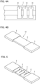
Figure 1] Figure 1A is a plan view showing a manufacturing step of a resistor of an embodiment; andFigure 1B is a sectional view taken along line A-A ofFigure 1A as seen from an arrow direction. - [
Figure 2] Figure 2A is a plan view showing a manufacturing step subsequent to the step as shown inFigure 1A; Figure 2B is a sectional view taken along line B-B ofFigure 2A as seen from an arrow direction; andFigure 2C is a sectional view of the structure that is different from the one as shown inFigure 2B . - [
Figure 3] Figure 3A is a sectional view showing a manufacturing step subsequent to the step as shown inFigure 2A ; andFigure 3B is a sectional view showing a manufacturing step subsequent to the step as shown inFigure 2B . - [
Figure 4] Figure 4A is a plan view showing a manufacturing step subsequent to the steps as shown inFigures 3A and 3B ; andFigure 4B is a perspective view of a resistor intermediate cut in the step as shown inFigure 4A . - [
Figure 5] Figure 5 is a perspective view showing a manufacturing step subsequent to the step as shown inFigure 4B . - [
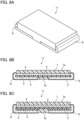
Figure 6] Figure 6A is a perspective view showing a manufacturing step subsequent to the step as shown inFigure 5 ;Figure 6B is a sectional view taken along line C-C ofFigure 6A in a thickness direction as seen from an arrow direction; andFigure 6C is a sectional view of a structure that has been formed using the resistor intermediate as shown inFigure 3B . - [
Figure 7] Figure 7A is a perspective view showing a manufacturing step subsequent to the step as shown inFigure 6A ;Figure 7B is a sectional view showing a manufacturing step subsequent to the step as shown inFigure 6B ; andFigure 7C is a sectional view showing a manufacturing step subsequent to the step as shown inFigure 6C . - [
Figure 8] Figure 8A is a perspective view showing a manufacturing step subsequent to the step as shown inFigure 7A ;Figure 8B is a sectional view showing a manufacturing step subsequent to the step as shown inFigure 7B ; andFigure 8C is a sectional view showing a manufacturing step subsequent to the step as shown inFigure 7C . - [
Figure 9] Figure 9 is a graph showing a DSC curve and a DDSC curve of a polyimide/epoxy resin. - [
Figure 10] Figure 10 is a graph showing the DSC curve of the polyimide/epoxy resin at a temperature fixed to 170°C. - An embodiment according to the present invention (hereinafter simply referred to as an "embodiment") will be described in detail. The present invention is not limited to the following embodiment, but may be implemented in various modifications within a scope of the appended claims.
- Referring to the drawings, a resistor manufacturing method of the embodiment will be described in the order of the manufacturing steps.
- In steps as shown in
Figures 1A and 1B , aresistive body 2 and a plurality ofelectrode plates 3 are prepared. Each of theresistive body 2 and theelectrode plates 3 has a flat plate shape or a belt-like shape. In the embodiment as shown inFigure 1A , each of theresistive body 2 and theelectrode plates 3 has the belt-like shape. - In the step as shown in
Figures 1A and 1B , theelectrode plates 3 are bonded to both sides of theresistive body 2, respectively through laser welding, for example, to produce a bondedbody 1. Besides the laser welding as an exemplified case, the existing bonding process may be executed. AsFigure 1A shows, thebonded body 1 may be constituted by bonding theresistive body 2 and theelectrode plates 3 into the belt-like shape. The above-described bondedbody 1 is wound in a roll, and placed on a production line. This makes it possible to execute the subsequent manufacturing steps automatically for mass-production of the resistors according to the embodiment. - In the embodiment, each thickness of the
resistive body 2 and theelectrode plate 3 is not limited. For example, theresistive body 2 may be formed to have the thickness ranging from several tens of µm to several hundreds of µm approximately. Theresistive body 2 may be formed to have substantially the same thickness as, or different thickness from that of theelectrode plate 3. - In the embodiment, existing material may be used for forming the
resistive body 2 and theelectrode plate 3 in a non-restrictive manner. For example, it is possible to use metal resistance material such as copper-nickel and nickel-chrome, a structure formed by applying a metal film onto the surface of an insulating base, a conductive ceramic substrate and the like for forming theresistive body 2. For example, it is possible to use copper, silver, nickel, chrome, and composite material thereof for forming theelectrode plate 3. - When bonding the
electrode plates 3 to both sides of theresistive body 2, respectively, each end surface of theresistive body 2 may be brought into abutment on the corresponding end surface of theelectrode plates 3 as shown inFigure 1B . Alternatively, theresistive body 2 and theelectrode plates 3 may be bonded while having the respective surfaces partially overlapped with each another. - The
resistive body 2 and theelectrode plates 3 may be integrally formed. That is, it is possible to use the single metal resistance plate as the same material for forming theresistive body 2 and theelectrode plates 3. Alternatively, plating of the metal material with low resistance is applied to the region to be formed as theelectrode plate 3 on the metal resistance plate so that theelectrode plate 3 is formed on the surface of the metal resistance plate. - In the steps as shown in
Figures 2A and 2B , an uncured first thermallyconductive layer 4 is formed on the surface of theresistive body 2. Preferably, the first thermallyconductive layer 4 is an electrically insulating thermosetting resin with high thermal conductivity. For example, the thermosetting resin such as epoxy and polyimide may be used for forming the first thermallyconductive layer 4. - The uncured first thermally
conductive layer 4 may be in the form of a film or a paste. In the case of the film, the uncured thermally conductive resin film is stuck on the surface of theresistive body 2. In the case of the paste, the uncured thermally conductive resin paste is applied to or printed on the surface of theresistive body 2. Alternatively, the first thermallyconductive layer 4 may be formed by executing the inkjet process. - In the embodiment, the thickness of the first thermally
conductive layer 4 is not limited. The thickness may be arbitrarily specified in consideration of the thermal conductivity of the resistor as the finished product, and secure fixation between the resistive body and the electrode plates. Especially, in the embodiment, there are two or more thermally conductive layers to be interposed between the resistive body and the electrode plates. It is therefore preferable to adjust the thickness of the first thermallyconductive layer 4 in consideration of the number of layers. For example, preferably, the thickness of the first thermallyconductive layer 4 is in the range from approximately 20 µm to 200 µm. - The term "uncured" refers to the state where the layer is not cured completely. Specifically, the uncured state where the layer has not been completely cured represents that curing reaction hardly proceeds to exhibit fluidity at the same level as that in the initial formation stage, or the state of the purchased product for shipment. The term "cured (completely cured)" refers to the state where the layer has lost the fluidity owing to accelerated polymerization due to linkage of molecules. For example, when the first thermally
conductive layer 4 is formed as the thermally conductive resin film, the pre-processing (temporary crimping) is executed after placing the first thermallyconductive layer 4 on theresistive body 2 as shown inFigure 2B . The state after executing the pre-processing is defined as being the "uncured" state. That is, in the pre-processing, heat is applied (equal to or lower than the application temperature) for a short time (for example, approximately several minutes) to adhere (temporary crimping) the first thermallyconductive layer 4 to theresistive body 2. The state after heating in the pre-processing is still in the "uncured" state. - When using the thermally conductive resin film for the first thermally
conductive layer 4, the first thermallyconductive layer 4 is in the uncured and solidified state. The term "solidified" refers to the state of having become solid. - Meanwhile, when using the thermally conductive resin paste for the first thermally
conductive layer 4, the first thermallyconductive layer 4 is in the uncured and unsolidified state. The term "unsolidified" refers to the state where the solid component is partially or entirely dispersed in the solvent such as slurry and ink. - In the embodiment, the first thermally
conductive layer 4 may be formed only on the surface of theresistive body 2 as shown inFigure 2B . However, it is possible to form the first thermallyconductive layer 4 on the entire surface from theresistive body 2 to theelectrode plates 3 as shown inFigure 2C . Alternatively, although not shown, it is possible to form the first thermallyconductive layer 4 on the surface from theresistive body 2 to a part of each of theelectrode plates 3. Alternatively, in the manufacturing step to be described below in which theelectrode plates 3 are bent, it is possible to form the first thermallyconductive layer 4 on the region except the bent parts. That is, the first thermallyconductive layer 4 may be formed in three divided parts on the respective surfaces of theresistive body 2 and theelectrode plates 3 except the boundary therebetween. - As
Figure 2C shows, the first thermallyconductive layer 4 is formed not only on the surface of theresistive body 2 but also on the surfaces of theelectrode plates 3. This makes it possible to facilitate formation of the first thermallyconductive layer 4. When using the thermally conductive resin film for the first thermallyconductive layer 4, for example, asFigure 2C shows, the thermally conductive resin film does not have to be positioned to theresistive body 2. The thermally conductive resin film that is large enough to cover theresistive body 2 and theelectrode plates 3 may be stuck on the surfaces of theresistive body 2 and theelectrode plates 3. Alternatively, when using the thermally conductive resin paste for the first thermallyconductive layer 4, the first thermallyconductive layer 4 may be applied to the surfaces of theresistive body 2 and theelectrode plates 3 entirely. As described above, the manufacturing step may be simplified by forming the first thermallyconductive layer 4 not only on the surface of theresistive body 2 but also on the surfaces of theelectrode plates 3. - Then the heating process is applied to the uncured first thermally
conductive layer 4 for complete curing. At this time, the use of the thermally conductive resin paste for the first thermallyconductive layer 4 may facilitate solidification and curing. The determination whether or not the layer has been completely cured may be made in accordance with the cure degree, viscosity, thermal processing condition and the like. It is possible to use the cure degree to be calculated from the calorific value derived from the measurement utilizing the differential scanning calorimeter. Complete curing refers to the condition where the cure degree is equal to or higher than 70%, or refers to the condition generally called stage C. - As the uncured first thermally
conductive layer 4 is cured, the thermally conductive layer having the film thickness hardly fluctuating is securely formed on the surface of theresistive body 2, or on the surfaces of theresistive body 2 and theelectrode plates 3 before theelectrode plates 3 are bent in the subsequent step. - Although it is not intended to limit the thermal processing condition for completely curing the first thermally
conductive layer 4, it is preferable to apply the heating process to the first thermallyconductive layer 4 at the temperature ranging from approximately 150°C to 250°C for approximately 0.5 to 2 hours. The heating temperature and the heating time required for curing may vary depending on the material for forming the first thermallyconductive layer 4. If the first thermallyconductive layer 4 is the purchased product, the curing condition is specified in accordance with the heating temperature and the heating time as prescribed by the manufacturer. For example, the heating temperature and the heating time of the resin used for the experiment to be described later are specified to be in the range from approximately 160°C to 200°C, and approximately 70 to 30 minutes (the lower the heating temperature becomes, the longer the heating time is set) for appropriate adjustment. - In the embodiment, subsequent to the step as shown in
Figure 2B , an uncured second thermallyconductive layer 5 is laminated on the surface of the first thermallyconductive layer 4 as shown inFigure 3A . Alternatively, subsequent to the step as shown inFigure 2C , the uncured second thermallyconductive layer 5 is laminated on the surface of the first thermallyconductive layer 4 as shown inFigure 3B . - In the embodiment, it is possible to use either the same or different material for forming the first thermally
conductive layer 4 as or from the material for the second thermallyconductive layer 5. It is also possible to use the thermally conductive resin film, or the thermally conductive resin paste for the second thermallyconductive layer 5. Accordingly, the second thermallyconductive layer 5 formed as the thermally conductive resin film is in the uncured and solidified state. Meanwhile, the second thermallyconductive layer 5 formed as the thermally conductive resin paste is in the uncured and unsolidified state. - In an exemplified case, the thermally conductive resin film may be used for the first thermally
conductive layer 4, and the thermally conductive resin film or the thermally conductive resin paste may be used for the second thermallyconductive layer 5. For example, it is preferable to use the same thermally conductive resin film for both the first thermallyconductive layer 4 and the second thermallyconductive layer 5 for improving productivity of the resistor. - The total value of thicknesses of the first thermally
conductive layer 4 and the second thermallyconductive layer 5, which are laminated is appropriately adjusted so that the interval between theresistive body 2 and theelectrode plates 3 is brought into a predetermined range after theelectrode plates 3 are bent in the subsequent step. - When using the thermally conductive resin film for the second thermally
conductive layer 5, the pre-processing is executed as described above so that the second thermallyconductive layer 5 is fixed to the first thermallyconductive layer 4. - As
Figure 4A shows, a resistor intermediate 10 is cut from the bondedbody 1 constituted by the completely cured first thermallyconductive layer 4 and the uncured second thermallyconductive layer 5.Figure 4B is a perspective view of the cut resistor intermediate 10. - As the belt-like bonded
body 1 as shown inFigure 4A is longitudinally fed, the plurality ofresistor intermediates 10 may be continuously cut by a press machine along the longitudinal direction. This makes it possible to mass-produce the resistor intermediates 10 in a short period of time. - The resistor intermediate 10 is constituted by the
resistive body 2 having a rectangular outer shape, and theelectrode plates 3 each having a rectangular outer shape provided at the respective sides of theresistive body 2. The outer shape of the resistor intermediate 10 as shown inFigure 4B is a mere example. It is therefore possible to form the resistor intermediate 10 to have the outer shape other than the one as shown inFigure 4B . - As
Figure 5 shows, a plurality ofcut portions 6 are formed in theresistive body 2 so that a meander pattern is formed for adjusting the resistance. Each length, each position, and the number of thecut portions 6 may be appropriately adjusted so that theresistive body 2 has a predetermined resistance value. The step as shown inFigure 5 may be executed as needed. - As
Figure 6A shows, theelectrode plates 3 are bent to the side of theresistive body 2, on which the first thermallyconductive layer 4 and the second thermallyconductive layer 5 are laminated, respectively. Referring toFigure 6A , as the first thermallyconductive layer 4 and the second thermallyconductive layer 5 are formed on the lower surface side of theresistive body 2, theelectrode plates 3 are bent toward the lower side. Each ofFigures 6B and 6C shows a cross section of theresistor 11 while omitting thecut portions 6 in theresistive body 2, which are expected to appear inFigures 6B and 6C . Each dimension ratio of the thickness and the length of theresistive body 2, theelectrode plates 3 and the thermallyconductive layer 4 is different between the cases as shown inFigures 3A and 3B , and the cases as shown inFigures 6B and 6C . The dimension ratio of the thickness and the length of theresistive body 2, theelectrode plates 3, and the thermallyconductive layer 4 as illustrated inFigures 3A and 3B is different from that as illustrated inFigures 6B and 6C . However, structures which are enlarged for illustration purposes are substantially the same from a physical viewpoint. - As
Figures 6A and 6B show, thebent electrode plates 3 confront the lower side of theresistive body 2 via the first thermallyconductive layer 4 and the second thermallyconductive layer 5. Likewise the case as shown inFigure 3A ,Figure 6B shows the structure constituted by using the resistor intermediate formed by laminating the first thermallyconductive layer 4 and the second thermallyconductive layer 5 on the surface of theresistive body 2, and bending theelectrode plates 3. Accordingly, the single first thermallyconductive layer 4 and the single second thermallyconductive layer 5 intervene between theresistive body 2 and thebent electrode plates 3. - Meanwhile, likewise the structure as shown in
Figure 3B ,Figure 6C shows the structure constituted by using the resistor intermediate formed by laminating the first thermallyconductive layer 4 and the second thermallyconductive layer 5 over the surfaces from theresistive body 2 to theelectrode plates 3 entirely, and bending theelectrode plates 3. Accordingly, the double-layered first thermallyconductive layer 4 and the double-layered second thermallyconductive layer 5 intervene between theresistive body 2 and thebent electrode plates 3. Referring toFigure 6C , the single layer of the first thermallyconductive layer 4 and the single layer of the second thermallyconductive layer 5 are laminated at the center part of theresistive body 2 to which theelectrode plates 3 do not confront. - The second thermally
conductive layer 5 in the uncured state is heated to be completely cured. The term "complete curing" refers to the explanation that has been already described as above. - In the embodiment, it is preferable to completely cure the second thermally
conductive layer 5 while pressing thebent electrode plates 3 toward theresistive body 2. That is, asFigure 6B shows, thebent electrode plates 3 are pressed while being in contact with the second thermallyconductive layer 5, and heated so that the second thermallyconductive layer 5 is completely cured. AsFigure 6C shows, the first thermallyconductive layer 4 and the second thermallyconductive layer 5 at the inner sides of thebent electrode plates 3 are pressed while being laminated with the first thermallyconductive layer 4 and the second thermallyconductive layer 5 on the lower surface of theresistive body 2, and heated so that the second thermallyconductive layers 5 are completely cured. This makes it possible to securely adhere and fix theresistive body 2 and theelectrode plates 3 via the first thermallyconductive layers 4 and the second thermallyconductive layers 5. - Then in the step as shown in
Figure 7A , aprotective layer 7 is mold-formed onto the surface of theresistive body 2. Preferably, theprotective layer 7 is formed of a material with excellent heat resisting and electrically insulating properties. Although it is not intended to limit the material for forming theprotective layer 7, the mold-forming of theprotective layer 7 may be executed using the resin, glass, organic material and the like. AsFigures 7B and 7C show, theprotective layer 7 includes a surfaceprotective layer 7a for covering the surface of theresistive body 2, and a bottom surfaceprotective layer 7b for filling the space between thebent electrode plates 3 at the lower surface side of theresistive body 2. AsFigures 7B and 7C show, the bottom surfaceprotective layer 7b and theelectrode plates 3 constitute substantially the flush bottom surface.Figure 7B shows the step subsequent to the one as shown inFigure 6B , andFigure 7C shows the step subsequent to the one as shown inFigure 6C . - It is possible to affix a seal on the surface of the surface protective layer.
- As
Figures 8A, 8B, and 8C show, plating is applied to surfaces of theelectrode plates 3. Although the material for forming aplating layer 8 is not limited, theplating layer 8 may be constituted by a Cu plating layer and an Ni plating layer, for example. Theplating layer 8 serves to expand the contact area to the substrate surface on which theresistor 11 is disposed, and suppress the soldering erosion of theelectrode plate 3 upon soldering of theresistor 11 to the substrate surface.Figure 8B represents the step subsequent to the one as shown inFigure 7B .Figure 8C represents the step subsequent to the one as shown inFigure 7C . The plating process is carried out as needed. - The
resistor 11 manufactured through the above-described manufacturing steps includes theresistive body 2, theelectrode plates 3 disposed at both sides of theresistive body 2, respectively while being bent at the lower surface side of theresistive body 2, and the plurality of cured thermallyconductive layers resistive body 2 and theelectrode plates 3 as shown inFigures 8B and 8C . - A total value of thicknesses of the plurality of thermally
conductive layers resistive body 2 and theelectrode plates 3 ranges from approximately 50 µm to 150 µm. Each thickness of the thermallyconductive layers resistive body 2 to theelectrode plates 3 via the thermallyconductive layers conductive layers resistive body 2 and theelectrode plates 3 to be made more uniform, and variation in the heat dissipation property may also be suppressed. This makes it possible to provide theresistor 11 with improved heat dissipation property. The total value of thicknesses of the thermallyconductive layers resistive body 2 and theelectrode plates 3. This makes it possible to appropriately prevent the failure such as peeling of theelectrode plate 3 from the thermally conductive layer, or crack generated in the thermally conductive layer. - The resistor manufacturing method of the embodiment is characterized in that, after completely curing the first thermally
conductive layer 4, the uncured second thermallyconductive layer 5 is laminated on the first thermally conductive layer, and thereafter, theelectrode plates 3 are bent, and the second thermallyconductive layer 5 is cured. - Execution of the above-described manufacturing steps allows suppression of variation in each thickness of the thermally
conductive layers resistive body 2 and theelectrode plates 3 compared with the generally employed steps. That is, upon execution of the heating process after bending of theelectrode plates 3, the first thermallyconductive layer 4 of those thermally conductive layers has been already cured, thus hardly causing the film thickness fluctuation. At this time, the second thermallyconductive layer 5 has been uncured. However, the second thermallyconductive layer 5 partially constitutes the thickness between theresistive body 2 and theelectrode plates 3. The variation in the thickness of the thermally conductive layer resulting from fluidity of the second thermallyconductive layer 5 may be made smaller than the case where the entire thermally conductive layer between theresistive body 2 and theelectrode plates 3 is in the uncured state. - As described above, in the embodiment, it is possible to suppress variation in the thickness of the thermally conductive layer between the
resistive body 2 and theelectrode plates 3. This makes it possible to make the thickness between theresistive body 2 and theelectrode plates 3 further uniform, and to suppress variation in the heat dissipation property, thus manufacturing theresistor 11 with excellent heat dissipation property. The further uniform thickness between theresistive body 2 and theelectrode plates 3 may suppress generation of a gap or the like between theresistive body 2 and theelectrode plates 3, resulting in improved adhesive strength. - The uncured and solidified material, specifically, the thermally conductive resin film may be preferably used for forming at least any one of the first thermally
conductive layer 4 and the second thermallyconductive layer 5. - When using the uncured and unsolidified material, specifically, the thermally conductive resin paste for forming both the first thermally
conductive layer 4 and the second thermallyconductive layer 5, the thickness between theresistive body 2 and theelectrode plates 3 is likely to vary. That is, intrinsically, the use of the thermally conductive resin paste is likely to vary the thickness in the state where the paste is applied. Consequently, the use of the thermally conductive resin film in the uncured and solidified state for forming at least one of the first thermallyconductive layer 4 and the second thermallyconductive layer 5 makes it possible to suppress the thickness variation between theresistive body 2 and theelectrode plates 3 more effectively. The use of the thermally conductive resin film for forming both the first thermallyconductive layer 4 and the second thermallyconductive layer 5 allows adjustment of the thickness between theresistive body 2 and theelectrode plates 3 so that the thickness is made further uniform. - For example, the thermally conductive resin film is used for forming the first thermally
conductive layer 4 to adjust so that the thickness between theresistive body 2 and theelectrode plates 3 is within a predetermined range. Meanwhile, the thermally conductive resin paste is thinly applied to form the second thermallyconductive layer 5 to adhere theelectrode plates 3. This makes it possible to easily adjust the thickness within the predetermined range while suppressing variation in the thickness between theresistive body 2 and theelectrode plates 3, and to securely adhere theelectrode plates 3. - In the steps as shown in
Figures 6A, 6B, and 6C , it is preferable to cure the second thermallyconductive layer 5 while pressing thebent electrode plates 3. This makes it possible to securely adhere theelectrode plates 3. - The present invention will be described in more detail based on an example implemented to exhibit the advantageous effect of the present invention. However, the present invention is not limited to the example as described below.
- In an experiment, the following resin was used, and the thermal analysis was carried out using a differential scanning calorimeter (DSC).
- The DSC curve and the DDSC curve were obtained at the temperature elevation rate of 10°C/min in the experiment.
- As
Figure 9 shows, the curing start temperature was 150°C, and the curing end temperature was 220°C. At the timing when the temperature becomes 230°C onward, transition of the phase to the combustion reaction was observed. - In accordance with the experimental result, the applied temperature was measured to be in the range from 160°C to 220°C.
- The temperature was fixed to 170°C to obtain the curing start temperature and the curing end temperature from the DSC curve in accordance with the holding time. The obtained experimental results are shown in
Figure 10 . -
Figure 10 shows that the curing started after a lapse of about 42 minutes, and the curing ended after a lapse of about 61 minutes. - The above-described experimental result has clarified that the resin to be used as specified above was cured under the condition at 170°C for approximately 60 minutes. The curing condition coincided with the curing condition recommended by the resin manufacturer.
- As the curing condition is established at 170°C for 60 minutes, the curing condition in the temperature range as shown in
Figure 9 may be established at 160°C for 70 minutes, 170°C for 60 minutes, 180°C for 50 minutes, 190°C for 40 minutes, and 200°C for 30 minutes approximately. - The resistor according to the present invention with excellent heat dissipation property allows reduction in its height. The resistor may be surface mounted so as to be mounted to various types of circuit boards.
- The present application claims priority from Japanese Patent Application No.
JP2017-237820 filed on December 12, 2017
Claims (4)
- A resistor manufacturing method comprising:a step of forming an uncured first thermally conductive layer (4) made of an electrically insulating thermosetting resin on a surface of a resistive body (2);a step of curing the first thermally conductive layer (4);a step of laminating an uncured second thermally conductive layer (5) made of an electrically insulating thermosetting resin on a surface of the first thermally conductive layer (4); anda step of bending electrode plates (3) respectively disposed at both sides of the resistive body (2), curing the second thermally conductive layer, and performing adhesion between the resistive body (2) and the electrode plates (3) via the first thermally conductive layer (4) and the second thermally conductive layer (5).
- The resistor manufacturing method according to claim 1, wherein at least any one of the first thermally conductive layer (4) and the second thermally conductive layer (5) is a thermally conductive resin film.
- The resistor manufacturing method according to claim 2, wherein at least any one of the first thermally conductive layer (4) and the second thermally conductive layer (5) is a thermally conductive resin film made of epoxy or polyimide.
- The resistor manufacturing method according to any one of claims 1 to 3, wherein the second thermally conductive layer is cured while having a pressure applied to the electrode plates (3) that have been bent so that the first thermally conductive layer (4) and the second thermally conductive layer (5) at the inner sides of the bent electrode plates (3) are pressed.
Applications Claiming Priority (2)
| Application Number | Priority Date | Filing Date | Title |
|---|---|---|---|
| JP2017237820A JP6573956B2 (en) | 2017-12-12 | 2017-12-12 | Resistor manufacturing method |
| PCT/JP2018/045456 WO2019117127A1 (en) | 2017-12-12 | 2018-12-11 | Resistor manufacturing method and resistor |
Publications (3)
| Publication Number | Publication Date |
|---|---|
| EP3726541A1 EP3726541A1 (en) | 2020-10-21 |
| EP3726541A4 EP3726541A4 (en) | 2021-12-29 |
| EP3726541B1 true EP3726541B1 (en) | 2025-06-04 |
Family
ID=66819690
Family Applications (1)
| Application Number | Title | Priority Date | Filing Date |
|---|---|---|---|
| EP18887518.1A Active EP3726541B1 (en) | 2017-12-12 | 2018-12-11 | Resistor manufacturing method |
Country Status (6)
| Country | Link |
|---|---|
| US (1) | US11462343B2 (en) |
| EP (1) | EP3726541B1 (en) |
| JP (1) | JP6573956B2 (en) |
| KR (1) | KR102296732B1 (en) |
| CN (1) | CN111465998B (en) |
| WO (1) | WO2019117127A1 (en) |
Family Cites Families (17)
| Publication number | Priority date | Publication date | Assignee | Title |
|---|---|---|---|---|
| JPS6015319Y2 (en) * | 1976-07-19 | 1985-05-14 | 北陸電気工業株式会社 | lead frame |
| JPS59177929U (en) * | 1983-05-13 | 1984-11-28 | 日本電気株式会社 | Resin-clad electronic components |
| JPS62290581A (en) | 1986-06-09 | 1987-12-17 | Mitsubishi Paper Mills Ltd | thermal transfer recording material |
| FR2640825B1 (en) * | 1988-12-20 | 1991-01-25 | Europ Composants Electron | ELECTRICAL COMPONENT WITH DIRECT REPORT |
| DE4339551C1 (en) * | 1993-11-19 | 1994-10-13 | Heusler Isabellenhuette | Resistor, constructed as a surface-mounted device, and method for its production, as well as a printed circuit board having such a resistor |
| WO1997006660A2 (en) * | 1995-08-15 | 1997-02-27 | Bourns, Multifuse (Hong Kong), Ltd. | Surface mount conductive polymer devices and method for manufacturing such devices |
| JP3846986B2 (en) * | 1997-11-21 | 2006-11-15 | 北陸電気工業株式会社 | Manufacturing method of chip resistor |
| DE19953594A1 (en) * | 1998-11-20 | 2000-05-25 | Matsushita Electric Industrial Co Ltd | Surface-mounted electronic component, e.g. a capacitor, has electrodes of migration resistant material formed on the entire surface of a substrate |
| JP3860515B2 (en) * | 2002-07-24 | 2006-12-20 | ローム株式会社 | Chip resistor |
| JP4012029B2 (en) * | 2002-09-30 | 2007-11-21 | コーア株式会社 | Metal plate resistor and manufacturing method thereof |
| US7190252B2 (en) * | 2005-02-25 | 2007-03-13 | Vishay Dale Electronics, Inc. | Surface mount electrical resistor with thermally conductive, electrically insulative filler and method for using same |
| EP1947656B1 (en) * | 2005-11-07 | 2017-04-19 | Littelfuse, Inc. | Ptc device |
| JP5135585B2 (en) * | 2008-07-25 | 2013-02-06 | セイコーインスツル株式会社 | Manufacturing method of thermal head |
| US8912876B2 (en) * | 2010-06-21 | 2014-12-16 | Koa Corporation | Surface mounting varistor |
| TWI600354B (en) * | 2014-09-03 | 2017-09-21 | 光頡科技股份有限公司 | Micro-resistance structure with high bending strength, manufacturing method thereof |
| KR101853170B1 (en) | 2015-12-22 | 2018-04-27 | 삼성전기주식회사 | Chip Resistor and method for manufacturing the same |
| US11011290B2 (en) * | 2017-12-12 | 2021-05-18 | Koa Corporation | Method for manufacturing resistor, and resistor |
-
2017
- 2017-12-12 JP JP2017237820A patent/JP6573956B2/en active Active
-
2018
- 2018-12-11 EP EP18887518.1A patent/EP3726541B1/en active Active
- 2018-12-11 KR KR1020207018158A patent/KR102296732B1/en active Active
- 2018-12-11 WO PCT/JP2018/045456 patent/WO2019117127A1/en not_active Ceased
- 2018-12-11 US US16/771,393 patent/US11462343B2/en active Active
- 2018-12-11 CN CN201880079608.4A patent/CN111465998B/en active Active
Also Published As
| Publication number | Publication date |
|---|---|
| JP2019106448A (en) | 2019-06-27 |
| EP3726541A4 (en) | 2021-12-29 |
| US11462343B2 (en) | 2022-10-04 |
| KR20200090866A (en) | 2020-07-29 |
| US20200395150A1 (en) | 2020-12-17 |
| WO2019117127A1 (en) | 2019-06-20 |
| JP6573956B2 (en) | 2019-09-11 |
| KR102296732B1 (en) | 2021-09-02 |
| EP3726541A1 (en) | 2020-10-21 |
| CN111465998B (en) | 2022-07-08 |
| CN111465998A (en) | 2020-07-28 |
Similar Documents
| Publication | Publication Date | Title |
|---|---|---|
| JP6487769B2 (en) | Manufacturing method of laminated busbar unit | |
| CN102891006B (en) | Electronic component and method for manufacturing electronic component | |
| JP6726821B2 (en) | Method of manufacturing semiconductor device | |
| EP3726542B1 (en) | Method for manufacturing resistor | |
| JP2010114167A (en) | Low-resistive chip resistor, and method for manufacturing the same | |
| US11011290B2 (en) | Method for manufacturing resistor, and resistor | |
| CN100544556C (en) | Multilayer printed circuit board and manufacture method thereof | |
| US11462343B2 (en) | Resistor manufacturing method and resistor | |
| US12477661B2 (en) | Chip component | |
| JP3012875B2 (en) | Manufacturing method of chip resistor | |
| JPH0553281B2 (en) | ||
| JPH10189306A (en) | Chip resistor | |
| JP2806802B2 (en) | Chip resistor | |
| JP3235826U (en) | High power resistor | |
| US20240096926A1 (en) | Mounting structure for chip component | |
| JP2000200701A (en) | Chip type resistor and its manufacture | |
| JP3323140B2 (en) | Chip resistor | |
| JP3323156B2 (en) | Chip resistor | |
| JP3435419B2 (en) | Chip resistor | |
| JPH09120905A (en) | Chip electronic part and method for manufacturing the same | |
| JP2015192024A (en) | Resistor manufacturing method |
Legal Events
| Date | Code | Title | Description |
|---|---|---|---|
| STAA | Information on the status of an ep patent application or granted ep patent |
Free format text: STATUS: THE INTERNATIONAL PUBLICATION HAS BEEN MADE |
|
| PUAI | Public reference made under article 153(3) epc to a published international application that has entered the european phase |
Free format text: ORIGINAL CODE: 0009012 |
|
| STAA | Information on the status of an ep patent application or granted ep patent |
Free format text: STATUS: REQUEST FOR EXAMINATION WAS MADE |
|
| 17P | Request for examination filed |
Effective date: 20200702 |
|
| AK | Designated contracting states |
Kind code of ref document: A1 Designated state(s): AL AT BE BG CH CY CZ DE DK EE ES FI FR GB GR HR HU IE IS IT LI LT LU LV MC MK MT NL NO PL PT RO RS SE SI SK SM TR |
|
| AX | Request for extension of the european patent |
Extension state: BA ME |
|
| DAV | Request for validation of the european patent (deleted) | ||
| DAX | Request for extension of the european patent (deleted) | ||
| RIC1 | Information provided on ipc code assigned before grant |
Ipc: H01C 1/02 20060101AFI20210727BHEP Ipc: H01C 1/148 20060101ALI20210727BHEP Ipc: H01C 7/00 20060101ALI20210727BHEP Ipc: H01C 17/02 20060101ALI20210727BHEP Ipc: H01C 13/00 20060101ALI20210727BHEP Ipc: H01C 17/07 20060101ALI20210727BHEP Ipc: H01C 1/028 20060101ALI20210727BHEP |
|
| REG | Reference to a national code |
Ref country code: DE Ref legal event code: R079 Free format text: PREVIOUS MAIN CLASS: H01C0017020000 Ipc: H01C0001020000 Ref country code: DE Ref legal event code: R079 Ref document number: 602018082477 Country of ref document: DE Free format text: PREVIOUS MAIN CLASS: H01C0017020000 Ipc: H01C0001020000 |
|
| A4 | Supplementary search report drawn up and despatched |
Effective date: 20211130 |
|
| RIC1 | Information provided on ipc code assigned before grant |
Ipc: H01C 1/028 20060101ALI20211124BHEP Ipc: H01C 17/07 20060101ALI20211124BHEP Ipc: H01C 13/00 20060101ALI20211124BHEP Ipc: H01C 17/02 20060101ALI20211124BHEP Ipc: H01C 7/00 20060101ALI20211124BHEP Ipc: H01C 1/148 20060101ALI20211124BHEP Ipc: H01C 1/02 20060101AFI20211124BHEP |
|
| GRAP | Despatch of communication of intention to grant a patent |
Free format text: ORIGINAL CODE: EPIDOSNIGR1 |
|
| STAA | Information on the status of an ep patent application or granted ep patent |
Free format text: STATUS: GRANT OF PATENT IS INTENDED |
|
| INTG | Intention to grant announced |
Effective date: 20250103 |
|
| GRAS | Grant fee paid |
Free format text: ORIGINAL CODE: EPIDOSNIGR3 |
|
| GRAA | (expected) grant |
Free format text: ORIGINAL CODE: 0009210 |
|
| STAA | Information on the status of an ep patent application or granted ep patent |
Free format text: STATUS: THE PATENT HAS BEEN GRANTED |
|
| AK | Designated contracting states |
Kind code of ref document: B1 Designated state(s): AL AT BE BG CH CY CZ DE DK EE ES FI FR GB GR HR HU IE IS IT LI LT LU LV MC MK MT NL NO PL PT RO RS SE SI SK SM TR |
|
| REG | Reference to a national code |
Ref country code: GB Ref legal event code: FG4D |
|
| REG | Reference to a national code |
Ref country code: CH Ref legal event code: EP |
|
| REG | Reference to a national code |
Ref country code: DE Ref legal event code: R096 Ref document number: 602018082477 Country of ref document: DE |
|
| REG | Reference to a national code |
Ref country code: IE Ref legal event code: FG4D |
|
| REG | Reference to a national code |
Ref country code: NL Ref legal event code: MP Effective date: 20250604 |
|
| PG25 | Lapsed in a contracting state [announced via postgrant information from national office to epo] |
Ref country code: FI Free format text: LAPSE BECAUSE OF FAILURE TO SUBMIT A TRANSLATION OF THE DESCRIPTION OR TO PAY THE FEE WITHIN THE PRESCRIBED TIME-LIMIT Effective date: 20250604 Ref country code: ES Free format text: LAPSE BECAUSE OF FAILURE TO SUBMIT A TRANSLATION OF THE DESCRIPTION OR TO PAY THE FEE WITHIN THE PRESCRIBED TIME-LIMIT Effective date: 20250604 |
|
| REG | Reference to a national code |
Ref country code: LT Ref legal event code: MG9D |
|
| PG25 | Lapsed in a contracting state [announced via postgrant information from national office to epo] |
Ref country code: GR Free format text: LAPSE BECAUSE OF FAILURE TO SUBMIT A TRANSLATION OF THE DESCRIPTION OR TO PAY THE FEE WITHIN THE PRESCRIBED TIME-LIMIT Effective date: 20250905 Ref country code: NO Free format text: LAPSE BECAUSE OF FAILURE TO SUBMIT A TRANSLATION OF THE DESCRIPTION OR TO PAY THE FEE WITHIN THE PRESCRIBED TIME-LIMIT Effective date: 20250904 |
|
| PG25 | Lapsed in a contracting state [announced via postgrant information from national office to epo] |
Ref country code: PL Free format text: LAPSE BECAUSE OF FAILURE TO SUBMIT A TRANSLATION OF THE DESCRIPTION OR TO PAY THE FEE WITHIN THE PRESCRIBED TIME-LIMIT Effective date: 20250604 |
|
| PG25 | Lapsed in a contracting state [announced via postgrant information from national office to epo] |
Ref country code: BG Free format text: LAPSE BECAUSE OF FAILURE TO SUBMIT A TRANSLATION OF THE DESCRIPTION OR TO PAY THE FEE WITHIN THE PRESCRIBED TIME-LIMIT Effective date: 20250604 |
|
| PG25 | Lapsed in a contracting state [announced via postgrant information from national office to epo] |
Ref country code: HR Free format text: LAPSE BECAUSE OF FAILURE TO SUBMIT A TRANSLATION OF THE DESCRIPTION OR TO PAY THE FEE WITHIN THE PRESCRIBED TIME-LIMIT Effective date: 20250604 |
|
| PG25 | Lapsed in a contracting state [announced via postgrant information from national office to epo] |
Ref country code: RS Free format text: LAPSE BECAUSE OF FAILURE TO SUBMIT A TRANSLATION OF THE DESCRIPTION OR TO PAY THE FEE WITHIN THE PRESCRIBED TIME-LIMIT Effective date: 20250904 |
|
| PG25 | Lapsed in a contracting state [announced via postgrant information from national office to epo] |
Ref country code: LV Free format text: LAPSE BECAUSE OF FAILURE TO SUBMIT A TRANSLATION OF THE DESCRIPTION OR TO PAY THE FEE WITHIN THE PRESCRIBED TIME-LIMIT Effective date: 20250604 |
|
| PG25 | Lapsed in a contracting state [announced via postgrant information from national office to epo] |
Ref country code: NL Free format text: LAPSE BECAUSE OF FAILURE TO SUBMIT A TRANSLATION OF THE DESCRIPTION OR TO PAY THE FEE WITHIN THE PRESCRIBED TIME-LIMIT Effective date: 20250604 |
|
| PG25 | Lapsed in a contracting state [announced via postgrant information from national office to epo] |
Ref country code: PT Free format text: LAPSE BECAUSE OF FAILURE TO SUBMIT A TRANSLATION OF THE DESCRIPTION OR TO PAY THE FEE WITHIN THE PRESCRIBED TIME-LIMIT Effective date: 20251006 |
|
| REG | Reference to a national code |
Ref country code: AT Ref legal event code: MK05 Ref document number: 1801208 Country of ref document: AT Kind code of ref document: T Effective date: 20250604 |
|
| PG25 | Lapsed in a contracting state [announced via postgrant information from national office to epo] |
Ref country code: IS Free format text: LAPSE BECAUSE OF FAILURE TO SUBMIT A TRANSLATION OF THE DESCRIPTION OR TO PAY THE FEE WITHIN THE PRESCRIBED TIME-LIMIT Effective date: 20251004 |
|
| PGFP | Annual fee paid to national office [announced via postgrant information from national office to epo] |
Ref country code: DE Payment date: 20251028 Year of fee payment: 8 |
|
| PG25 | Lapsed in a contracting state [announced via postgrant information from national office to epo] |
Ref country code: SM Free format text: LAPSE BECAUSE OF FAILURE TO SUBMIT A TRANSLATION OF THE DESCRIPTION OR TO PAY THE FEE WITHIN THE PRESCRIBED TIME-LIMIT Effective date: 20250604 Ref country code: AT Free format text: LAPSE BECAUSE OF FAILURE TO SUBMIT A TRANSLATION OF THE DESCRIPTION OR TO PAY THE FEE WITHIN THE PRESCRIBED TIME-LIMIT Effective date: 20250604 |
|
| PG25 | Lapsed in a contracting state [announced via postgrant information from national office to epo] |
Ref country code: CZ Free format text: LAPSE BECAUSE OF FAILURE TO SUBMIT A TRANSLATION OF THE DESCRIPTION OR TO PAY THE FEE WITHIN THE PRESCRIBED TIME-LIMIT Effective date: 20250604 |
|
| PG25 | Lapsed in a contracting state [announced via postgrant information from national office to epo] |
Ref country code: EE Free format text: LAPSE BECAUSE OF FAILURE TO SUBMIT A TRANSLATION OF THE DESCRIPTION OR TO PAY THE FEE WITHIN THE PRESCRIBED TIME-LIMIT Effective date: 20250604 |
|
| PG25 | Lapsed in a contracting state [announced via postgrant information from national office to epo] |
Ref country code: RO Free format text: LAPSE BECAUSE OF FAILURE TO SUBMIT A TRANSLATION OF THE DESCRIPTION OR TO PAY THE FEE WITHIN THE PRESCRIBED TIME-LIMIT Effective date: 20250604 Ref country code: SK Free format text: LAPSE BECAUSE OF FAILURE TO SUBMIT A TRANSLATION OF THE DESCRIPTION OR TO PAY THE FEE WITHIN THE PRESCRIBED TIME-LIMIT Effective date: 20250604 |
|
| PG25 | Lapsed in a contracting state [announced via postgrant information from national office to epo] |
Ref country code: IT Free format text: LAPSE BECAUSE OF FAILURE TO SUBMIT A TRANSLATION OF THE DESCRIPTION OR TO PAY THE FEE WITHIN THE PRESCRIBED TIME-LIMIT Effective date: 20250604 |
|
| REG | Reference to a national code |
Ref country code: DE Ref legal event code: R097 Ref document number: 602018082477 Country of ref document: DE |
|
| PLBE | No opposition filed within time limit |
Free format text: ORIGINAL CODE: 0009261 |
|
| STAA | Information on the status of an ep patent application or granted ep patent |
Free format text: STATUS: NO OPPOSITION FILED WITHIN TIME LIMIT |
|
| PG25 | Lapsed in a contracting state [announced via postgrant information from national office to epo] |
Ref country code: DK Free format text: LAPSE BECAUSE OF FAILURE TO SUBMIT A TRANSLATION OF THE DESCRIPTION OR TO PAY THE FEE WITHIN THE PRESCRIBED TIME-LIMIT Effective date: 20250604 |
|
| REG | Reference to a national code |
Ref country code: CH Ref legal event code: L10 Free format text: ST27 STATUS EVENT CODE: U-0-0-L10-L00 (AS PROVIDED BY THE NATIONAL OFFICE) Effective date: 20260416 |
|
| 26N | No opposition filed |
Effective date: 20260305 |