EP3726228A1 - Current sensor - Google Patents
Current sensor Download PDFInfo
- Publication number
- EP3726228A1 EP3726228A1 EP18888921.6A EP18888921A EP3726228A1 EP 3726228 A1 EP3726228 A1 EP 3726228A1 EP 18888921 A EP18888921 A EP 18888921A EP 3726228 A1 EP3726228 A1 EP 3726228A1
- Authority
- EP
- European Patent Office
- Prior art keywords
- connector
- circuit board
- case
- magnetic sensor
- current sensor
- Prior art date
- Legal status (The legal status is an assumption and is not a legal conclusion. Google has not performed a legal analysis and makes no representation as to the accuracy of the status listed.)
- Granted
Links
Images



Classifications
-
- G—PHYSICS
- G01—MEASURING; TESTING
- G01R—MEASURING ELECTRIC VARIABLES; MEASURING MAGNETIC VARIABLES
- G01R15/00—Details of measuring arrangements of the types provided for in groups G01R17/00 - G01R29/00, G01R33/00 - G01R33/26 or G01R35/00
- G01R15/14—Adaptations providing voltage or current isolation, e.g. for high-voltage or high-current networks
- G01R15/20—Adaptations providing voltage or current isolation, e.g. for high-voltage or high-current networks using galvano-magnetic devices, e.g. Hall-effect devices, i.e. measuring a magnetic field via the interaction between a current and a magnetic field, e.g. magneto resistive or Hall effect devices
- G01R15/207—Constructional details independent of the type of device used
-
- G—PHYSICS
- G01—MEASURING; TESTING
- G01R—MEASURING ELECTRIC VARIABLES; MEASURING MAGNETIC VARIABLES
- G01R19/00—Arrangements for measuring currents or voltages or for indicating presence or sign thereof
- G01R19/0092—Measuring current only
Definitions
- the present invention relates to a current sensor that calculates a current value according to a magnetic field generated by a current under measurement.
- a current sensor described in PTL 1 is known as a current sensor that calculates a current value according to a magnetic field generated by a current.
- conductors in each of which a current under measurement flows and magnetic sensors each of which measures an induced magnetic field generated by the current under measurement are accommodated in a case having a lid.
- the current sensor has magnetic shields fixed by being integrally formed in the bottom portion and lid portion of the case.
- a signal from the magnetic sensor can be output to the outside by exposing a connector mounted on a circuit board at an opening portion formed in a side wall of the case and connecting a connector from the outside.
- the current sensor described in PTL 1 is formed so that a connector is provided at an end of the circuit board and the attachment and removal direction of a connector on the other side to be connected is parallel to the surface of the circuit board. Therefore, even when the connector on the other side is inserted or removed, a force is not so largely applied in a direction perpendicular to the surface of the circuit board.
- the present invention addresses the above problem with the object of providing a current sensor that does not affect precision of the sensor even when a connector is inserted or removed.
- a current sensor of the present invention is characterized by having: a bus bar in which a current flows; a magnetic sensor that detects an induced magnetic field generated by the current flowing in the bus bar; an insulative circuit board on which the magnetic sensor is mounted; a connector mounted on the circuit board and connected to the magnetic sensor through the circuit board, the connector being capable of outputting a signal from the magnetic sensor to the outside; and a case having a case body and a lid portion, the case housing the circuit board and part of the bus bar.
- the current sensor is further characterized in that: the circuit board is fixed to the case body with a plurality of fixing portions, and the magnetic sensor is provided in a fixed area enclosed by the plurality of fixing portions; the connector is provided in an extended area extending from the fixed area; and stoppers are provided inside the case body and lid portion so as to face the front surface and rear surface of the extended portion through gaps.
- the magnetic sensor is provided in the fixed area enclosed by a plurality of fixing portions, and the connector is provided in the extended area extending from the fixed area.
- stoppers are provided on the front surface and rear surface of the extended area so as to face through gaps. Therefore, when a connector on the other side is inserted into or removed from the connector, the extended portion can be warped in the plate thickness direction only by an amount equal to the gap with respect to the stopper. Since the fixed area is enclosed by the plurality of fixing portions, the warp is suppressed. Therefore, no change occurs in a positional relationship between the bus bar and the magnetic sensor, so precision of the current sensor can be assured.
- the magnetic sensor is preferably placed so that a sensitivity direction for the induced magnetic field becomes the X direction in an XY plane; of the plurality of fixing portions, a first fixing portion placed between the magnetic sensor and the connector is preferably placed at two positions in the X direction; and the extended portion in which the connector is provided is preferably adjacent to the fixed area with the first fixing portions interposed.
- the first fixing portion is placed at two positions in the X direction between the magnetic sensor and the connector. Therefore, when the connector is inserted or removed, if the extended portion, in which the connector is fixed, is warped, the warp in the X direction is suppressed by the first fixing portions at the two positions. Due to this, the warp in the X direction is suppressed in the fixed area as well, so the effect is not exerted on the sensitivity direction. This can assure precision of the current sensor.
- the fixing portions preferably include a second fixing portion formed at one position opposite to the first fixing portions toward the Y direction with the magnetic sensor interposed.
- the fixed area becomes triangular by being enclosed by the fixing portions at two positions in the X direction and the fixing portion at one position in the Y direction. Therefore, even if the extended portion is warped, the warp in the fixed portion is suppressed to a minimum.
- the current sensor of the present invention when a magnetic shield is provided in the lid portion, no change occurs in a positional relationship between the magnetic shield and the magnetic sensor, so precision of the current sensor having the magnetic shield can be assured.
- a current sensor in a current sensor that outputs an output to the outside through a connector, a current sensor can be provided that does not affect precision of the sensor even when a connector is inserted or removed.
- the current sensor 1 in this embodiment is a sensor that can be used in a device requiring a large current such as a controller used in, for example, a hybrid vehicle or an electric car.
- Fig. 1 is a perspective view indicating the outside shape of the current sensor 1, which is an example of an embodiment of the present invention.
- Fig. 2 indicates a state in which the lid portion 12 of the current sensor 1 is removed.
- a lid-portion magnetic shield 17 provided in the lid portion 12 and a magnetic sensor 5 provided on a circuit board 4 are indicated by the dotted lines.
- Fig. 3 is an exploded view of the current sensor 1, indicating a state in which a bus bar 2 is separated from a case body 11, the circuit board 4 is separated from the case body 11, and the lid portion 12 is reversed.
- the current sensor 1 in this embodiment has the bus bar 2 in which a current flows and a case 10 that houses part of the bus bar 2.
- the case 10 is composed of the case body 11 in a box shape, the upper surface of which is open, and the lid portion 12 that covers the upper surface of the case body 11.
- the case body 11 and lid portion 12 are both made of an insulative synthetic resin. They are mutually fixed with two fixing screws 3.
- the insulative circuit board 4 is fixed with caulking portions 13, 14, and 15 at three positions and is housed inside the case body 11.
- These caulking portions 13, 14, and 15 are formed by making part of the case body 11 protrude in a columnar form, inserting the columnar portions into caulking holes 24, which will be described later, and thermally deforming the columnar portions from above.
- the caulking portions 13, 14, and 15 are equivalent to a plurality of fixing parts in the present invention.
- the caulking portions 13, 14, and 15 are composed of the caulking portions 13 and 14, which are aligned in the X direction in Fig. 2 , and the caulking portion 15 disposed at one position distant to the right of the caulking portions 13 and 14 in the Y direction.
- the caulking portions 13 and 14 are each equivalent to a first fixing portion in the present invention
- the caulking portion 15 is equivalent to a second fixing portion in the present invention.
- the caulking portion 15, which is the second fixing portion, is disposed at a position opposite to the caulking portions 13 and 14, each of which is the first fixing portion, in the Y direction with the magnetic sensor 5 interposed.
- a case-body-side magnetic shield 16 formed integrally with a resin is provided (see Fig. 4 to Fig. 6 ).
- an area enclosed by the caulking portions 13, 14, and 15 at three positions is a fixed area 4a.
- an area to the left of the caulking portions 13 and 14 in the Y direction in Fig. 2 is an extended portion 4b extending from the fixed area 4a. That is, the extended portion 4b is provided with the caulking portions 13 and 14, equivalent to the first fixing portions, interposed.
- a connector 6, which will be described later, is mounted on the extended portion 4b. Therefore, the connector 6 is mounted at a position at which the connector 6 does not overlap the fixed area 4a in the X direction, which is the direction of an induced magnetic field. Also, since the caulking portions 13 and 14 are aligned in a direction parallel to the short side of the circuit board 4, the extended portion 4b, on which the connector 6 is mounted, is likely to be bent.
- the magnetic sensor 5 is mounted on the rear surface of the fixed area 4a on the circuit board 4.
- the magnetic sensor 5 is a sensor that detects an induced magnetic field generated by a current flowing in the bus bar 2.
- the magnetic sensor 5 is fixed to the circuit board 4 so that the sensitivity direction of the magnetic sensor 5 for the induced magnetic field becomes the X direction, indicated by the arrow S in Fig. 2 , of an XY plane.
- the connector 6 is mounted on the front surface of the extended portion 4b on the circuit board 4.
- a conductive terminal (omitted in the drawing) provided in the connector 6 is connected to a circuit pattern (omitted in the drawing) provided on the circuit board 4 and is connected to the magnetic sensor 5 through the circuit board 4.
- the connector 6 is connected to a connector (omitted in the drawing, also true hereinafter) of another device so that a signal from the magnetic sensor 5 can be output to the outside of the case 10.
- a metallic lid-portion magnetic shield 17 is provided in the lid portion 12.
- the lid-portion magnetic shield 17 is placed in a mold (omitted in the drawing, also true hereinafter) for injection molding and is molded integrally with a resin, which is a raw material.
- a connector opening 18 is formed through which the connector 6 is exposed to the outside.
- two lid-side stoppers 19 are provided in the vicinity of the connector opening 18 on the rear surface side, as indicated in Fig. 3 .
- a Y-direction positioning protrusion 20 is provided at two positions on outer walls enclosing the circumference on the rear surface side of the lid portion 12. The Y-direction positioning protrusion 20 performs positioning in the Y direction with respect to the case body 11.
- an X-direction positioning recess21 is provided at two positions in the X direction of the outer walls.
- the X-direction positioning recesses 21 perform positioning in the X direction.
- a lid-side Z-direction positioning portion 23 performing positioning in the Z direction.
- the circuit board 4 is an insulative plate member in a substantially quadrangle shape, and caulking holes 24 through which the caulking portions 13, 14, and 15 provided inside the case body 11 are passed are formed on the circuit board 4 at three positions.
- a case-body-side stopper 25 (stopper) facing the rear surface of the circuit board 4 is provided at three positions. Also, in Fig. 3 , the caulking portions 13, 14, and 15 yet to be caulked to the circuit board 4 are indicated, so they are in a columnar shape so that they can be passed through the caulking holes 24 in the circuit board 4.
- a Y-direction positioning recess 26 performing positioning in the Y direction and an X-direction positioning protrusions 27 performing positioning in the X direction are each formed at two positions. Also, in the vicinity of a screw hole 28 in which the fixing screw 3 is fastened, a body-side Z-direction positioning portion 29 performing positioning in the Z direction is formed.
- the bus bar 2 is a plate-like member extending in the Y direction.
- a to-be-detected portion 2a facing the magnetic sensor 5 is formed so that the width in X direction is narrower than the other portions.
- a cutout 2b is formed in one side edge of the bus bar 2. This cutout 2b is used for positioning by using a positioning protrusion (omitted in the drawing) of the mold for injection molding when the bus bar 2 is formed integrally inside the case body 11. This prevents the bus bar 2 from being attached to the case body 11 in the opposite direction.
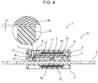
- Fig. 4 is a cross-sectional view along line IV-IV in Fig. 1 at the center position of the current sensor 1 in the X direction.
- Fig. 5 is a cross-sectional view along line V-V when a portion closer to the outer wall at front than in Fig. 4 is cut.
- the circuit board 4 is positioned and fixed to the case body 11 with the caulking portions 13 and 15.
- the magnetic sensor 5 is mounted in the fixed area 4a.
- the connector 6 is mounted in the extended portion 4b.
- the case-body-side stopper 25 is placed so as to face the extended portion 4b with a gap G left between them.
- the lid-side stopper 19 is placed so as to face the circuit board 4 with the gap G left between them, as indicated in Fig. 5 .
- the case-body-side stopper 25 is placed so as to face the extended portion 4b with the gap G left between them.
- the minimum value of this gap G is set so that in consideration of the dimensional tolerances of the lid-side stopper 19, case-body-side stopper 25, and circuit board 4, even when the stopper side and circuit board 4 come closest to each other, the gap G does not become smaller than zero.
- the maximum value of the gap G is set to a magnitude enough to prevent a change in an output from the magnetic sensor 5 due to a positional relationship among the magnetic sensor 5, the caulking portions 13, 14, and 15, and the connector 6 on the circuit board 4 even when the extended portion 4b is warped.
- the gap G is set so that it falls within a range from 0 mm to 0.1 mm.
- the lid-side Z-direction positioning portion 23 and body-side Z-direction positioning portion 29 abut each other as indicated in Fig. 5 to position the lid portion 12 and case body 11 in the Z direction. At other positions, a gap g is formed between the outer wall portions of the lid portion 12 and case body 11.
- the positioning of the lid portion 12 and case body 11 in the X direction is performed by fitting to the X-direction positioning recesses 21 provided in the lid portion 12 and to the X-direction positioning protrusions 27 provided on the case body 11, as indicated in Fig. 1 .
- positioning in the Y direction is performed by fitting to the Y-direction positioning protrusions 20 provided on the lid portion 12 and to the Y-direction positioning recesses 26 provided in the case body 11.
- Fig. 6 is a perspective view when the current sensor 1 in this embodiment is viewed from rear surface side.
- a recess 30 is formed, which is formed by a shield pressing portion (omitted in the drawing) provided in the mold for injection molding when the case-body-side magnetic shield 16 is molded integrally in the case body 11.
- a total eight recesses 30 are provided, two for each of the four edges of the case-body-side magnetic shield 16.
- each circle indicated by a dotted line on a side surface of the case body 11 is a gate position 31 of the mold for injection molding.
- the dash-dot line extending in the Y direction at the center of the case-body-side magnetic shield 16 is a so-called weld line 32 on a resin. Incidentally, as a product, this weld line 32 does not appear on the front surface.
- the recess 30 formed when the case-body-side magnetic shield 16 is supported in the mold for injection molding is provided at two positions deviated from the weld line 32 in the X direction. Due to this, the structure is such that even if distortion occurs in the case body 11 and a stress is thereby generated in the weld line 32, cracks are not easily generated from the weld line 32.
- the current sensor 1 in this embodiment has the structure described above, when a connector of another device is inserted into the connector 6, the connector 6 is pressed against the circuit board 4 in the Z direction. At this time, the extended portion 4b on the circuit board 4 is warped downward in the Z direction with the line interconnecting the caulking portions 13 and 14, which are the first fixing portion, taken as the boundary.
- the fixed area 4a, enclosed by the caulking portions 13, 14, and 15, on the circuit board 4 is slightly affected by the warp of the extended portion 4b.
- the warp of the extended portion 4b is eliminated, so the effect does not remain in the positional relationship between the magnetic sensor 5 mounted on the fixed area 4a and the to-be-detected portion 2a of the bus bar 2.
- the caulking portions 13 and 14 are aligned in the X direction and this alignment direction matches the sensitivity direction S of the magnetic sensor 5. Therefore, even if a slight change occurs in the position of the fixed area 4a, in which the magnetic sensor 5 is mounted, due to the effect caused in the connector 6, the sensitivity direction S of the magnetic sensor 5 is not changed. Thus, there is no practical effect on the sensitivity of the magnetic sensor 5.
- the magnetic sensor 5 is not affected by the insertion or removal of a connector of another device into or from the connector 6, or even if the magnetic sensor 5 is affected, the magnetic sensor 5 is not practically affected. Therefore, the precision of the current sensor 1 can be stably maintained.
- the gap G between the circuit board 4 and the lid-side stopper 19 and case-body-side stopper 25 is preferably small. However, it is necessary to prevent the gap G from being reduced below zero even if the gap G is minimized due to the dimensional tolerances of individual members. This is because if the gap G becomes negative, the lid-side stopper 19 or case-body-side stopper 25 is kept in contact with the circuit board 4, placing the circuit board 4 in a deformed state, so the extended portion 4b is warped and the position of the magnetic sensor 5 in the fixed area 4a is also affected.
- the fixing portions that fix the circuit board 4 to the case body 11 are the caulking portions 13 and 14 provided as the first fixing portions, and the caulking portion 15 provided as the second fixing portion.
- the fixed area 4a is formed with three caulking portions 13, 14, and 15 in this way, the fixed area 4a becomes triangular and thereby becomes less likely to be externally affected.
- caulking portions 13, 14, and 15 are set at three positions, this is not a limitation. Caulking portions may be set at four or more positions. Also, in the above embodiment, although the gap G between the circuit board 4 and the lid-side stopper 19 and the gap G between the circuit board 4 and the case-body-side stopper 25 are a common magnitude, this is not a limitation. Different dimensions may be set.
- the case 10 is composed of two members, lid portion 12 and case body 11, and the lid portion 12 is formed so as to have a smaller thickness than the case body 11.
- the thickness of the lid portion 12 may be larger than the thickness of the case body 11 without being limited to the shape in the above embodiment.
- the fixing portions that fix the circuit board 4 and case body 11 together are the caulking portions 13, 14, and 15, this is not a limitation. Press fitting the caulking hole 24 to a columnar portion formed inside the case body 11 may be performed. Alternatively, other fixing means such as screwing or riveting may be used.
- each stopper is formed by a protrusion in an elliptical shape, this is not a limitation.
- Other shapes such as a columnar shape and prismatic shape suffice if they can minimize the warp of the circuit board 4.
- the lid-portion magnetic shield 17 and case-body-side magnetic shield 16 are formed integrally in the lid portion 12 and case body 11 and are fixed.
- the lid-portion magnetic shield 17 and case-body-side magnetic shield 16 may be fixed by using caulking portions as with the circuit board 4 or in another fixing method.
Landscapes
- Physics & Mathematics (AREA)
- General Physics & Mathematics (AREA)
- Measuring Instrument Details And Bridges, And Automatic Balancing Devices (AREA)
Abstract
Description
- The present invention relates to a current sensor that calculates a current value according to a magnetic field generated by a current under measurement.
- A current sensor described in
PTL 1 is known as a current sensor that calculates a current value according to a magnetic field generated by a current. In the current sensor described inPTL 1, conductors in each of which a current under measurement flows and magnetic sensors each of which measures an induced magnetic field generated by the current under measurement are accommodated in a case having a lid. The current sensor has magnetic shields fixed by being integrally formed in the bottom portion and lid portion of the case. - In the current sensor in
PTL 1, a signal from the magnetic sensor can be output to the outside by exposing a connector mounted on a circuit board at an opening portion formed in a side wall of the case and connecting a connector from the outside. - PTL 1: Japanese Unexamined Patent Application
- Publication No.
2017-102022 - The current sensor described in
PTL 1 is formed so that a connector is provided at an end of the circuit board and the attachment and removal direction of a connector on the other side to be connected is parallel to the surface of the circuit board. Therefore, even when the connector on the other side is inserted or removed, a force is not so largely applied in a direction perpendicular to the surface of the circuit board. - On the other hand, with a current sensor, there is a case in which the connector is mounted in a direction perpendicular to the surface of the circuit board due to a positional relationship of a device to be connected or another reason. In this case, when the connector on the other side is inserted into or removed from the connector on the circuit board side, a force is applied directly in a direction perpendicular to the surface of the circuit board. Therefore, there is the fear that distortion occurs in the circuit board.
- If distortion occurs in the circuit board as described above, there is the fear that a change occurs in a clearance between the conductor and a magnetic sensor mounted on the circuit board and a clearance between the magnetic sensor and the magnetic shield and the precision of the magnetic sensor is thereby lowered.
- In a current sensor that outputs an output to the outside through a connector, the present invention addresses the above problem with the object of providing a current sensor that does not affect precision of the sensor even when a connector is inserted or removed.
- To achieve the above object, a current sensor of the present invention is characterized by having: a bus bar in which a current flows; a magnetic sensor that detects an induced magnetic field generated by the current flowing in the bus bar; an insulative circuit board on which the magnetic sensor is mounted; a connector mounted on the circuit board and connected to the magnetic sensor through the circuit board, the connector being capable of outputting a signal from the magnetic sensor to the outside; and a case having a case body and a lid portion, the case housing the circuit board and part of the bus bar. The current sensor is further characterized in that: the circuit board is fixed to the case body with a plurality of fixing portions, and the magnetic sensor is provided in a fixed area enclosed by the plurality of fixing portions; the connector is provided in an extended area extending from the fixed area; and stoppers are provided inside the case body and lid portion so as to face the front surface and rear surface of the extended portion through gaps.
- According to the current sensor of the present invention, the magnetic sensor is provided in the fixed area enclosed by a plurality of fixing portions, and the connector is provided in the extended area extending from the fixed area. Also, stoppers are provided on the front surface and rear surface of the extended area so as to face through gaps. Therefore, when a connector on the other side is inserted into or removed from the connector, the extended portion can be warped in the plate thickness direction only by an amount equal to the gap with respect to the stopper. Since the fixed area is enclosed by the plurality of fixing portions, the warp is suppressed. Therefore, no change occurs in a positional relationship between the bus bar and the magnetic sensor, so precision of the current sensor can be assured.
- In the current sensor of the present invention, the magnetic sensor is preferably placed so that a sensitivity direction for the induced magnetic field becomes the X direction in an XY plane; of the plurality of fixing portions, a first fixing portion placed between the magnetic sensor and the connector is preferably placed at two positions in the X direction; and the extended portion in which the connector is provided is preferably adjacent to the fixed area with the first fixing portions interposed.
- According to the current sensor of the present invention, the first fixing portion is placed at two positions in the X direction between the magnetic sensor and the connector. Therefore, when the connector is inserted or removed, if the extended portion, in which the connector is fixed, is warped, the warp in the X direction is suppressed by the first fixing portions at the two positions. Due to this, the warp in the X direction is suppressed in the fixed area as well, so the effect is not exerted on the sensitivity direction. This can assure precision of the current sensor.
- Also, in the current sensor of the present invention, the fixing portions preferably include a second fixing portion formed at one position opposite to the first fixing portions toward the Y direction with the magnetic sensor interposed. According to this structure, the fixed area becomes triangular by being enclosed by the fixing portions at two positions in the X direction and the fixing portion at one position in the Y direction. Therefore, even if the extended portion is warped, the warp in the fixed portion is suppressed to a minimum.
- Also, in the current sensor of the present invention, when a magnetic shield is provided in the lid portion, no change occurs in a positional relationship between the magnetic shield and the magnetic sensor, so precision of the current sensor having the magnetic shield can be assured.
- According to the present invention, in a current sensor that outputs an output to the outside through a connector, a current sensor can be provided that does not affect precision of the sensor even when a connector is inserted or removed.
-
- [
Fig. 1] Fig. 1 is a perspective view indicating the outside shape of a current sensor, which is an example of an embodiment of the present invention. - [
Fig. 2] Fig. 2 is an explanatory diagram indicating a state in which the lid portion of the current sensor inFig. 1 is removed. - [
Fig. 3] Fig. 3 is a perspective view indicating a state in which the current sensor inFig 2 is further disassembled and the lid portion is reversed. - [
Fig. 4] Fig. 4 is a cross-sectional view of the current sensor inFig. 1 as taken along line IV-IV. - [
Fig. 5] Fig. 5 is a cross-sectional view of the current sensor inFig. 1 as taken along line V-V. - [
Fig. 6] Fig. 6 is a perspective view indicating a state as viewed from the rear surface of the current sensor inFig. 1 . - Next, a current sensor, which is an example of an embodiment of the present invention, will be described with reference to
Fig. 1 to Fig. 6 . Thecurrent sensor 1 in this embodiment is a sensor that can be used in a device requiring a large current such as a controller used in, for example, a hybrid vehicle or an electric car. -
Fig. 1 is a perspective view indicating the outside shape of thecurrent sensor 1, which is an example of an embodiment of the present invention.Fig. 2 indicates a state in which thelid portion 12 of thecurrent sensor 1 is removed. A lid-portionmagnetic shield 17 provided in thelid portion 12 and amagnetic sensor 5 provided on acircuit board 4 are indicated by the dotted lines.Fig. 3 is an exploded view of thecurrent sensor 1, indicating a state in which abus bar 2 is separated from acase body 11, thecircuit board 4 is separated from thecase body 11, and thelid portion 12 is reversed. - As indicated in
Fig. 1 , thecurrent sensor 1 in this embodiment has thebus bar 2 in which a current flows and acase 10 that houses part of thebus bar 2. As indicated inFig. 2 , thecase 10 is composed of thecase body 11 in a box shape, the upper surface of which is open, and thelid portion 12 that covers the upper surface of thecase body 11. Thecase body 11 andlid portion 12 are both made of an insulative synthetic resin. They are mutually fixed with twofixing screws 3. - Also, as indicated in
Fig. 2 , theinsulative circuit board 4 is fixed withcaulking portions case body 11. Thesecaulking portions case body 11 protrude in a columnar form, inserting the columnar portions into caulkingholes 24, which will be described later, and thermally deforming the columnar portions from above. Thecaulking portions - In this embodiment, the
caulking portions caulking portions Fig. 2 , and thecaulking portion 15 disposed at one position distant to the right of thecaulking portions caulking portions caulking portion 15 is equivalent to a second fixing portion in the present invention. - The
caulking portion 15, which is the second fixing portion, is disposed at a position opposite to thecaulking portions magnetic sensor 5 interposed. Incidentally, in thecase body 11, a case-body-sidemagnetic shield 16 formed integrally with a resin is provided (seeFig. 4 to Fig. 6 ). - In this embodiment, of an area on the
circuit board 4, an area enclosed by thecaulking portions fixed area 4a. Also, on thecircuit board 4, an area to the left of thecaulking portions Fig. 2 is an extendedportion 4b extending from thefixed area 4a. That is, the extendedportion 4b is provided with thecaulking portions connector 6, which will be described later, is mounted on theextended portion 4b. Therefore, theconnector 6 is mounted at a position at which theconnector 6 does not overlap the fixedarea 4a in the X direction, which is the direction of an induced magnetic field. Also, since thecaulking portions circuit board 4, theextended portion 4b, on which theconnector 6 is mounted, is likely to be bent. - The
magnetic sensor 5 is mounted on the rear surface of the fixedarea 4a on thecircuit board 4. Themagnetic sensor 5 is a sensor that detects an induced magnetic field generated by a current flowing in thebus bar 2. In this embodiment, themagnetic sensor 5 is fixed to thecircuit board 4 so that the sensitivity direction of themagnetic sensor 5 for the induced magnetic field becomes the X direction, indicated by the arrow S inFig. 2 , of an XY plane. - The
connector 6 is mounted on the front surface of theextended portion 4b on thecircuit board 4. A conductive terminal (omitted in the drawing) provided in theconnector 6 is connected to a circuit pattern (omitted in the drawing) provided on thecircuit board 4 and is connected to themagnetic sensor 5 through thecircuit board 4. Also, theconnector 6 is connected to a connector (omitted in the drawing, also true hereinafter) of another device so that a signal from themagnetic sensor 5 can be output to the outside of thecase 10. - As indicated in
Fig. 2 , a metallic lid-portionmagnetic shield 17 is provided in thelid portion 12. In this embodiment, when thelid portion 12 is formed, the lid-portionmagnetic shield 17 is placed in a mold (omitted in the drawing, also true hereinafter) for injection molding and is molded integrally with a resin, which is a raw material. Also, in thelid portion 12, aconnector opening 18 is formed through which theconnector 6 is exposed to the outside. - In the
lid portion 12, two lid-side stoppers 19 (stoppers) are provided in the vicinity of theconnector opening 18 on the rear surface side, as indicated inFig. 3 . Also, a Y-direction positioning protrusion 20 is provided at two positions on outer walls enclosing the circumference on the rear surface side of thelid portion 12. The Y-direction positioning protrusion 20 performs positioning in the Y direction with respect to thecase body 11. - Similarly, an X-direction positioning recess21 is provided at two positions in the X direction of the outer walls. The X-direction positioning recesses 21 perform positioning in the X direction. Also, on the rear side of the
lid portion 12, the vicinity of aninsertion hole 22 into which the fixingscrew 3 is inserted is a lid-side Z-direction positioning portion 23 performing positioning in the Z direction. - As indicated in
Fig. 3 , thecircuit board 4 is an insulative plate member in a substantially quadrangle shape, and caulking holes 24 through which thecaulking portions case body 11 are passed are formed on thecircuit board 4 at three positions. - Inside the
case body 11, a case-body-side stopper 25 (stopper) facing the rear surface of thecircuit board 4 is provided at three positions. Also, inFig. 3 , thecaulking portions circuit board 4 are indicated, so they are in a columnar shape so that they can be passed through the caulking holes 24 in thecircuit board 4. - At outer wall portions of the
case body 11, a Y-direction positioning recess 26 performing positioning in the Y direction and anX-direction positioning protrusions 27 performing positioning in the X direction are each formed at two positions. Also, in the vicinity of ascrew hole 28 in which the fixingscrew 3 is fastened, a body-side Z-direction positioning portion 29 performing positioning in the Z direction is formed. - The
bus bar 2 is a plate-like member extending in the Y direction. A to-be-detected portion 2a facing themagnetic sensor 5 is formed so that the width in X direction is narrower than the other portions. Also, acutout 2b is formed in one side edge of thebus bar 2. Thiscutout 2b is used for positioning by using a positioning protrusion (omitted in the drawing) of the mold for injection molding when thebus bar 2 is formed integrally inside thecase body 11. This prevents thebus bar 2 from being attached to thecase body 11 in the opposite direction. - Next, the internal structure of the
current sensor 1 in this embodiment will be described with reference toFig. 4 andFig. 5 .Fig. 4 is a cross-sectional view along line IV-IV inFig. 1 at the center position of thecurrent sensor 1 in the X direction.Fig. 5 is a cross-sectional view along line V-V when a portion closer to the outer wall at front than inFig. 4 is cut. - As indicated in
Fig. 4 , thecircuit board 4 is positioned and fixed to thecase body 11 with thecaulking portions circuit board 4, themagnetic sensor 5 is mounted in the fixedarea 4a. On the front surface side, theconnector 6 is mounted in theextended portion 4b. On the rear surface side of theextended portion 4b on thecircuit board 4, the case-body-side stopper 25 is placed so as to face theextended portion 4b with a gap G left between them. - On the front surface side of the
extended portion 4b on thecircuit board 4, the lid-side stopper 19 is placed so as to face thecircuit board 4 with the gap G left between them, as indicated inFig. 5 . Also, on the rear surface side of theextended portion 4b on thecircuit board 4, the case-body-side stopper 25 is placed so as to face theextended portion 4b with the gap G left between them. - In this embodiment, the minimum value of this gap G is set so that in consideration of the dimensional tolerances of the lid-
side stopper 19, case-body-side stopper 25, andcircuit board 4, even when the stopper side andcircuit board 4 come closest to each other, the gap G does not become smaller than zero. - Also, the maximum value of the gap G is set to a magnitude enough to prevent a change in an output from the
magnetic sensor 5 due to a positional relationship among themagnetic sensor 5, thecaulking portions connector 6 on thecircuit board 4 even when theextended portion 4b is warped. In this embodiment, the gap G is set so that it falls within a range from 0 mm to 0.1 mm. - Also, as for the outer wall portions of the
lid portion 12 andcase body 11, the lid-side Z-direction positioning portion 23 and body-side Z-direction positioning portion 29 abut each other as indicated inFig. 5 to position thelid portion 12 andcase body 11 in the Z direction. At other positions, a gap g is formed between the outer wall portions of thelid portion 12 andcase body 11. - Also, the positioning of the
lid portion 12 andcase body 11 in the X direction is performed by fitting to the X-direction positioning recesses 21 provided in thelid portion 12 and to theX-direction positioning protrusions 27 provided on thecase body 11, as indicated inFig. 1 . Similarly, positioning in the Y direction is performed by fitting to the Y-direction positioning protrusions 20 provided on thelid portion 12 and to the Y-direction positioning recesses 26 provided in thecase body 11. -
Fig. 6 is a perspective view when thecurrent sensor 1 in this embodiment is viewed from rear surface side. In the rear surface of thecase body 11, arecess 30 is formed, which is formed by a shield pressing portion (omitted in the drawing) provided in the mold for injection molding when the case-body-sidemagnetic shield 16 is molded integrally in thecase body 11. In this embodiment, a total eightrecesses 30 are provided, two for each of the four edges of the case-body-sidemagnetic shield 16. - Here, in
Fig. 6 , the position of each circle indicated by a dotted line on a side surface of thecase body 11 is agate position 31 of the mold for injection molding. Also, inFig. 6 , the dash-dot line extending in the Y direction at the center of the case-body-sidemagnetic shield 16 is a so-calledweld line 32 on a resin. Incidentally, as a product, thisweld line 32 does not appear on the front surface. - In this embodiment, the
recess 30 formed when the case-body-sidemagnetic shield 16 is supported in the mold for injection molding is provided at two positions deviated from theweld line 32 in the X direction. Due to this, the structure is such that even if distortion occurs in thecase body 11 and a stress is thereby generated in theweld line 32, cracks are not easily generated from theweld line 32. - Since the
current sensor 1 in this embodiment has the structure described above, when a connector of another device is inserted into theconnector 6, theconnector 6 is pressed against thecircuit board 4 in the Z direction. At this time, theextended portion 4b on thecircuit board 4 is warped downward in the Z direction with the line interconnecting thecaulking portions - Since three case-body-
side stoppers 25 are provided on the rear surface side of theextended portion 4b as indicated inFig. 3 , even if theextended portion 4b is warped as described above, theextended portion 4b is just warped by an amount equal to the gap G due to the case-body-side stoppers 25. After the connector of the other device has been attached, theextended portion 4b returns to the previous position due to its elasticity, eliminating the warp of thecircuit board 4. - At this time, the fixed
area 4a, enclosed by thecaulking portions circuit board 4 is slightly affected by the warp of theextended portion 4b. However, after the connector of the other device has bee attached, the warp of theextended portion 4b is eliminated, so the effect does not remain in the positional relationship between themagnetic sensor 5 mounted on the fixedarea 4a and the to-be-detected portion 2a of thebus bar 2. - Also, the
caulking portions magnetic sensor 5. Therefore, even if a slight change occurs in the position of the fixedarea 4a, in which themagnetic sensor 5 is mounted, due to the effect caused in theconnector 6, the sensitivity direction S of themagnetic sensor 5 is not changed. Thus, there is no practical effect on the sensitivity of themagnetic sensor 5. - As described above, according to the
current sensor 1 in this embodiment, themagnetic sensor 5 is not affected by the insertion or removal of a connector of another device into or from theconnector 6, or even if themagnetic sensor 5 is affected, themagnetic sensor 5 is not practically affected. Therefore, the precision of thecurrent sensor 1 can be stably maintained. - In the above embodiment, to suppress the warp of the
extended portion 4b, the gap G between thecircuit board 4 and the lid-side stopper 19 and case-body-side stopper 25 is preferably small. However, it is necessary to prevent the gap G from being reduced below zero even if the gap G is minimized due to the dimensional tolerances of individual members. This is because if the gap G becomes negative, the lid-side stopper 19 or case-body-side stopper 25 is kept in contact with thecircuit board 4, placing thecircuit board 4 in a deformed state, so theextended portion 4b is warped and the position of themagnetic sensor 5 in the fixedarea 4a is also affected. - Also, in the above embodiment, the fixing portions that fix the
circuit board 4 to thecase body 11 are thecaulking portions caulking portion 15 provided as the second fixing portion. When the fixedarea 4a is formed with threecaulking portions area 4a becomes triangular and thereby becomes less likely to be externally affected. - Incidentally, in the above embodiment, although the
caulking portions circuit board 4 and the lid-side stopper 19 and the gap G between thecircuit board 4 and the case-body-side stopper 25 are a common magnitude, this is not a limitation. Different dimensions may be set. - Also, the
case 10 is composed of two members,lid portion 12 andcase body 11, and thelid portion 12 is formed so as to have a smaller thickness than thecase body 11. However, the thickness of thelid portion 12 may be larger than the thickness of thecase body 11 without being limited to the shape in the above embodiment. - Also, in the above embodiment, although the fixing portions that fix the
circuit board 4 andcase body 11 together are thecaulking portions caulking hole 24 to a columnar portion formed inside thecase body 11 may be performed. Alternatively, other fixing means such as screwing or riveting may be used. - Also, in the above embodiment, although each stopper is formed by a protrusion in an elliptical shape, this is not a limitation. Other shapes such as a columnar shape and prismatic shape suffice if they can minimize the warp of the
circuit board 4. - Also, in the above embodiment, the lid-portion
magnetic shield 17 and case-body-sidemagnetic shield 16 are formed integrally in thelid portion 12 andcase body 11 and are fixed. However, this is not a limitation. The lid-portionmagnetic shield 17 and case-body-sidemagnetic shield 16 may be fixed by using caulking portions as with thecircuit board 4 or in another fixing method. -
- 1
- current sensor
- 2
- bus bar
- 4
- circuit board
- 4a
- fixed area
- 4b
- extended portion
- 5
- magnetic sensor
- 6
- connector
- 10
- case
- 11
- case body
- 12
- lid portion
- 13
- to 15: caulking portion
- 16
- case-body-side magnetic shield
- 17
- lid-portion magnetic shield
- 18
- connector opening
- 19
- lid-side stopper
- 25
- case-body-side stopper
Claims (4)
- A current sensor comprising:a bus bar in which a current flows;a magnetic sensor that detects an induced magnetic field generated by the current flowing in the bus bar;an insulative circuit board on which the magnetic sensor is mounted;a connector mounted on the circuit board and connected to the magnetic sensor through the circuit board, the connector being capable of outputting a signal from the magnetic sensor to an outside; anda case having a case body and a lid portion, the case housing the circuit board and part of the bus bar; whereinthe circuit board is fixed to the case body with a plurality of fixing portions, and the magnetic sensor is provided in a fixed area enclosed by the plurality of fixing portions,the connector is provided in an extended area extending from the fixed area, andstoppers are provided inside the case body and the lid portion so as to face a front surface and rear surface of the extended portion through gaps.
- The current sensor according to Claim 1, wherein:the magnetic sensor is placed so that a sensitivity direction for the induced magnetic field becomes an X direction in an XY plane;of the plurality of fixing portions, a first fixing portion placed between the magnetic sensor and the connector is placed at two positions in the X direction; andthe extended portion in which the connector is provided is adjacent to the fixed area with the first fixing portions interposed.
- The current sensor according to Claim 2, wherein the fixing portions include a second fixing portion formed at one position opposite to the first fixing portions toward the Y direction with the magnetic sensor interposed.
- The current sensor according to any one of Claims 1 to 3, wherein a magnetic shield is provided in the lid portion.
Applications Claiming Priority (2)
| Application Number | Priority Date | Filing Date | Title |
|---|---|---|---|
| JP2017238494 | 2017-12-13 | ||
| PCT/JP2018/045575 WO2019117174A1 (en) | 2017-12-13 | 2018-12-11 | Current sensor |
Publications (3)
| Publication Number | Publication Date |
|---|---|
| EP3726228A1 true EP3726228A1 (en) | 2020-10-21 |
| EP3726228A4 EP3726228A4 (en) | 2021-08-25 |
| EP3726228B1 EP3726228B1 (en) | 2023-06-07 |
Family
ID=66819355
Family Applications (1)
| Application Number | Title | Priority Date | Filing Date |
|---|---|---|---|
| EP18888921.6A Active EP3726228B1 (en) | 2017-12-13 | 2018-12-11 | Current sensor |
Country Status (5)
| Country | Link |
|---|---|
| US (1) | US11287451B2 (en) |
| EP (1) | EP3726228B1 (en) |
| JP (1) | JP6890679B2 (en) |
| CN (1) | CN111465861B (en) |
| WO (1) | WO2019117174A1 (en) |
Families Citing this family (9)
| Publication number | Priority date | Publication date | Assignee | Title |
|---|---|---|---|---|
| JP7003620B2 (en) * | 2017-12-14 | 2022-01-20 | 日立金属株式会社 | Current sensor |
| JP7087512B2 (en) * | 2018-03-20 | 2022-06-21 | 株式会社デンソー | Current sensor |
| CN116583674A (en) * | 2020-11-09 | 2023-08-11 | 皮尔伯格泵技术有限责任公司 | electric coolant pump |
| KR20250073411A (en) * | 2022-10-24 | 2025-05-27 | 알프스 알파인 가부시키가이샤 | Current sensor |
| FR3145212B1 (en) * | 2023-01-20 | 2026-02-27 | Electricfil Automotive | Current detection assembly and motor block including such a detection assembly. |
| JP2024106683A (en) * | 2023-01-27 | 2024-08-08 | 株式会社デンソー | Current Sensors |
| US12283805B2 (en) * | 2023-03-30 | 2025-04-22 | BorgWarner US Technologies LLC | Bus bar assembly |
| US12598708B2 (en) * | 2023-11-30 | 2026-04-07 | Caterpillar Inc. | Detachable sensor assembly for an elongate conductor |
| CN118731448B (en) * | 2024-09-04 | 2024-11-15 | 宁波中车时代传感技术有限公司 | Integrated body of IGBT chemical current sensor |
Family Cites Families (19)
| Publication number | Priority date | Publication date | Assignee | Title |
|---|---|---|---|---|
| JP2522218Y2 (en) * | 1992-02-21 | 1997-01-08 | 矢崎総業株式会社 | Connector board fixing structure |
| CA2195830C (en) * | 1996-01-31 | 2000-05-16 | Kouichi Uezono | Connector fixing construction |
| JP5669076B2 (en) * | 2009-03-25 | 2015-02-12 | パナソニックIpマネジメント株式会社 | Substrate fixing structure and physical quantity sensor |
| JP5414333B2 (en) | 2009-04-09 | 2014-02-12 | 矢崎総業株式会社 | Current detector assembly structure |
| JP2011064648A (en) * | 2009-09-18 | 2011-03-31 | Tokai Rika Co Ltd | Current sensor |
| JP5872758B2 (en) * | 2010-04-28 | 2016-03-01 | 矢崎総業株式会社 | Current detector |
| JP2013015431A (en) * | 2011-07-05 | 2013-01-24 | Sumitomo Wiring Syst Ltd | Current detecting device |
| EP2546660A1 (en) * | 2011-07-13 | 2013-01-16 | LEM Intellectual Property SA | Electrical current sensor with grounded magnetic core |
| JP2013113631A (en) * | 2011-11-25 | 2013-06-10 | Yazaki Corp | Current detector |
| JP5817508B2 (en) * | 2011-12-22 | 2015-11-18 | 住友電装株式会社 | Current detector |
| DE202012103071U1 (en) * | 2012-08-14 | 2012-09-24 | Rauschert Heinersdorf-Pressig Gmbh | Measuring device for a contactless current measurement |
| JP6372969B2 (en) * | 2012-12-03 | 2018-08-15 | 矢崎総業株式会社 | Current sensor |
| WO2015033541A1 (en) * | 2013-09-05 | 2015-03-12 | 旭化成エレクトロニクス株式会社 | Current sensor |
| JP2015145839A (en) * | 2014-02-03 | 2015-08-13 | 株式会社フジクラ | Current detection device |
| JP2015145838A (en) * | 2014-02-03 | 2015-08-13 | 株式会社フジクラ | Current detection device and current detection device equipped with bus bar |
| JP6570811B2 (en) * | 2014-04-10 | 2019-09-04 | 日立金属株式会社 | connector |
| JP6477089B2 (en) * | 2014-05-23 | 2019-03-06 | 株式会社デンソー | Bus bar module with current sensor |
| JP6076952B2 (en) * | 2014-11-21 | 2017-02-08 | 矢崎総業株式会社 | Board terminal and board with terminal |
| WO2018012034A1 (en) * | 2016-07-15 | 2018-01-18 | アルプス電気株式会社 | Current sensor |
-
2018
- 2018-12-11 CN CN201880079733.5A patent/CN111465861B/en active Active
- 2018-12-11 JP JP2019559677A patent/JP6890679B2/en active Active
- 2018-12-11 WO PCT/JP2018/045575 patent/WO2019117174A1/en not_active Ceased
- 2018-12-11 EP EP18888921.6A patent/EP3726228B1/en active Active
-
2020
- 2020-06-11 US US16/899,322 patent/US11287451B2/en active Active
Also Published As
| Publication number | Publication date |
|---|---|
| CN111465861A (en) | 2020-07-28 |
| WO2019117174A1 (en) | 2019-06-20 |
| CN111465861B (en) | 2022-12-30 |
| EP3726228A4 (en) | 2021-08-25 |
| JP6890679B2 (en) | 2021-06-18 |
| EP3726228B1 (en) | 2023-06-07 |
| US20200300896A1 (en) | 2020-09-24 |
| US11287451B2 (en) | 2022-03-29 |
| JPWO2019117174A1 (en) | 2020-10-01 |
Similar Documents
| Publication | Publication Date | Title |
|---|---|---|
| EP3726228B1 (en) | Current sensor | |
| US10634702B2 (en) | Current sensor | |
| JP6198061B2 (en) | Wiring module | |
| US8854036B2 (en) | Current detecting apparatus | |
| US20190207347A1 (en) | Shielded connector | |
| JP7550128B2 (en) | Connectors and connector pairs | |
| US8947083B2 (en) | Current detecting apparatus | |
| KR101289526B1 (en) | Electronic unit case and method of manufacturing electronic unit | |
| KR20170130282A (en) | Electrical connector and production method thereof | |
| US11366139B2 (en) | Device and method for mounting a magnetic field sensor chip on a busbar | |
| JP2015216829A (en) | Electronic component unit and wire harness | |
| CN112526192A (en) | Integrated chip type current sensor and manufacturing method thereof | |
| US20180331525A1 (en) | Electrical connection box | |
| CN111465862A (en) | current sensor | |
| US20190372247A1 (en) | Circuit connection device | |
| US8348680B2 (en) | Daughter card assemblies | |
| EP3726229B1 (en) | Current sensor | |
| CN101499633B (en) | Electric connection box | |
| CN101499634A (en) | Electric connection box | |
| JP2012247241A (en) | Current detector | |
| CN114175867B (en) | electronic module | |
| US20200076114A1 (en) | Holding frame for a plug connector or a mounting flange for holding a circuit board | |
| JP2016065736A (en) | Current sensor | |
| JP2013044671A (en) | Current detector | |
| JP7472280B2 (en) | Current Sensors |
Legal Events
| Date | Code | Title | Description |
|---|---|---|---|
| STAA | Information on the status of an ep patent application or granted ep patent |
Free format text: STATUS: THE INTERNATIONAL PUBLICATION HAS BEEN MADE |
|
| PUAI | Public reference made under article 153(3) epc to a published international application that has entered the european phase |
Free format text: ORIGINAL CODE: 0009012 |
|
| STAA | Information on the status of an ep patent application or granted ep patent |
Free format text: STATUS: REQUEST FOR EXAMINATION WAS MADE |
|
| 17P | Request for examination filed |
Effective date: 20200707 |
|
| AK | Designated contracting states |
Kind code of ref document: A1 Designated state(s): AL AT BE BG CH CY CZ DE DK EE ES FI FR GB GR HR HU IE IS IT LI LT LU LV MC MK MT NL NO PL PT RO RS SE SI SK SM TR |
|
| AX | Request for extension of the european patent |
Extension state: BA ME |
|
| DAV | Request for validation of the european patent (deleted) | ||
| DAX | Request for extension of the european patent (deleted) | ||
| A4 | Supplementary search report drawn up and despatched |
Effective date: 20210723 |
|
| RIC1 | Information provided on ipc code assigned before grant |
Ipc: G01R 15/20 20060101AFI20210719BHEP |
|
| STAA | Information on the status of an ep patent application or granted ep patent |
Free format text: STATUS: EXAMINATION IS IN PROGRESS |
|
| 17Q | First examination report despatched |
Effective date: 20220420 |
|
| GRAP | Despatch of communication of intention to grant a patent |
Free format text: ORIGINAL CODE: EPIDOSNIGR1 |
|
| STAA | Information on the status of an ep patent application or granted ep patent |
Free format text: STATUS: GRANT OF PATENT IS INTENDED |
|
| RIC1 | Information provided on ipc code assigned before grant |
Ipc: G01R 19/00 20060101ALI20221012BHEP Ipc: G01R 15/20 20060101AFI20221012BHEP |
|
| INTG | Intention to grant announced |
Effective date: 20221031 |
|
| GRAS | Grant fee paid |
Free format text: ORIGINAL CODE: EPIDOSNIGR3 |
|
| GRAA | (expected) grant |
Free format text: ORIGINAL CODE: 0009210 |
|
| STAA | Information on the status of an ep patent application or granted ep patent |
Free format text: STATUS: THE PATENT HAS BEEN GRANTED |
|
| AK | Designated contracting states |
Kind code of ref document: B1 Designated state(s): AL AT BE BG CH CY CZ DE DK EE ES FI FR GB GR HR HU IE IS IT LI LT LU LV MC MK MT NL NO PL PT RO RS SE SI SK SM TR |
|
| REG | Reference to a national code |
Ref country code: GB Ref legal event code: FG4D |
|
| REG | Reference to a national code |
Ref country code: CH Ref legal event code: EP Ref country code: AT Ref legal event code: REF Ref document number: 1576685 Country of ref document: AT Kind code of ref document: T Effective date: 20230615 |
|
| REG | Reference to a national code |
Ref country code: DE Ref legal event code: R096 Ref document number: 602018051625 Country of ref document: DE |
|
| REG | Reference to a national code |
Ref country code: LT Ref legal event code: MG9D |
|
| REG | Reference to a national code |
Ref country code: NL Ref legal event code: MP Effective date: 20230607 |
|
| PG25 | Lapsed in a contracting state [announced via postgrant information from national office to epo] |
Ref country code: SE Free format text: LAPSE BECAUSE OF FAILURE TO SUBMIT A TRANSLATION OF THE DESCRIPTION OR TO PAY THE FEE WITHIN THE PRESCRIBED TIME-LIMIT Effective date: 20230607 Ref country code: NO Free format text: LAPSE BECAUSE OF FAILURE TO SUBMIT A TRANSLATION OF THE DESCRIPTION OR TO PAY THE FEE WITHIN THE PRESCRIBED TIME-LIMIT Effective date: 20230907 Ref country code: ES Free format text: LAPSE BECAUSE OF FAILURE TO SUBMIT A TRANSLATION OF THE DESCRIPTION OR TO PAY THE FEE WITHIN THE PRESCRIBED TIME-LIMIT Effective date: 20230607 |
|
| REG | Reference to a national code |
Ref country code: AT Ref legal event code: MK05 Ref document number: 1576685 Country of ref document: AT Kind code of ref document: T Effective date: 20230607 |
|
| PG25 | Lapsed in a contracting state [announced via postgrant information from national office to epo] |
Ref country code: RS Free format text: LAPSE BECAUSE OF FAILURE TO SUBMIT A TRANSLATION OF THE DESCRIPTION OR TO PAY THE FEE WITHIN THE PRESCRIBED TIME-LIMIT Effective date: 20230607 Ref country code: NL Free format text: LAPSE BECAUSE OF FAILURE TO SUBMIT A TRANSLATION OF THE DESCRIPTION OR TO PAY THE FEE WITHIN THE PRESCRIBED TIME-LIMIT Effective date: 20230607 Ref country code: LV Free format text: LAPSE BECAUSE OF FAILURE TO SUBMIT A TRANSLATION OF THE DESCRIPTION OR TO PAY THE FEE WITHIN THE PRESCRIBED TIME-LIMIT Effective date: 20230607 Ref country code: LT Free format text: LAPSE BECAUSE OF FAILURE TO SUBMIT A TRANSLATION OF THE DESCRIPTION OR TO PAY THE FEE WITHIN THE PRESCRIBED TIME-LIMIT Effective date: 20230607 Ref country code: HR Free format text: LAPSE BECAUSE OF FAILURE TO SUBMIT A TRANSLATION OF THE DESCRIPTION OR TO PAY THE FEE WITHIN THE PRESCRIBED TIME-LIMIT Effective date: 20230607 Ref country code: GR Free format text: LAPSE BECAUSE OF FAILURE TO SUBMIT A TRANSLATION OF THE DESCRIPTION OR TO PAY THE FEE WITHIN THE PRESCRIBED TIME-LIMIT Effective date: 20230908 |
|
| PG25 | Lapsed in a contracting state [announced via postgrant information from national office to epo] |
Ref country code: FI Free format text: LAPSE BECAUSE OF FAILURE TO SUBMIT A TRANSLATION OF THE DESCRIPTION OR TO PAY THE FEE WITHIN THE PRESCRIBED TIME-LIMIT Effective date: 20230607 |
|
| PG25 | Lapsed in a contracting state [announced via postgrant information from national office to epo] |
Ref country code: SK Free format text: LAPSE BECAUSE OF FAILURE TO SUBMIT A TRANSLATION OF THE DESCRIPTION OR TO PAY THE FEE WITHIN THE PRESCRIBED TIME-LIMIT Effective date: 20230607 |
|
| PG25 | Lapsed in a contracting state [announced via postgrant information from national office to epo] |
Ref country code: IS Free format text: LAPSE BECAUSE OF FAILURE TO SUBMIT A TRANSLATION OF THE DESCRIPTION OR TO PAY THE FEE WITHIN THE PRESCRIBED TIME-LIMIT Effective date: 20231007 |
|
| PG25 | Lapsed in a contracting state [announced via postgrant information from national office to epo] |
Ref country code: SM Free format text: LAPSE BECAUSE OF FAILURE TO SUBMIT A TRANSLATION OF THE DESCRIPTION OR TO PAY THE FEE WITHIN THE PRESCRIBED TIME-LIMIT Effective date: 20230607 Ref country code: SK Free format text: LAPSE BECAUSE OF FAILURE TO SUBMIT A TRANSLATION OF THE DESCRIPTION OR TO PAY THE FEE WITHIN THE PRESCRIBED TIME-LIMIT Effective date: 20230607 Ref country code: RO Free format text: LAPSE BECAUSE OF FAILURE TO SUBMIT A TRANSLATION OF THE DESCRIPTION OR TO PAY THE FEE WITHIN THE PRESCRIBED TIME-LIMIT Effective date: 20230607 Ref country code: PT Free format text: LAPSE BECAUSE OF FAILURE TO SUBMIT A TRANSLATION OF THE DESCRIPTION OR TO PAY THE FEE WITHIN THE PRESCRIBED TIME-LIMIT Effective date: 20231009 Ref country code: IS Free format text: LAPSE BECAUSE OF FAILURE TO SUBMIT A TRANSLATION OF THE DESCRIPTION OR TO PAY THE FEE WITHIN THE PRESCRIBED TIME-LIMIT Effective date: 20231007 Ref country code: EE Free format text: LAPSE BECAUSE OF FAILURE TO SUBMIT A TRANSLATION OF THE DESCRIPTION OR TO PAY THE FEE WITHIN THE PRESCRIBED TIME-LIMIT Effective date: 20230607 Ref country code: CZ Free format text: LAPSE BECAUSE OF FAILURE TO SUBMIT A TRANSLATION OF THE DESCRIPTION OR TO PAY THE FEE WITHIN THE PRESCRIBED TIME-LIMIT Effective date: 20230607 Ref country code: AT Free format text: LAPSE BECAUSE OF FAILURE TO SUBMIT A TRANSLATION OF THE DESCRIPTION OR TO PAY THE FEE WITHIN THE PRESCRIBED TIME-LIMIT Effective date: 20230607 |
|
| PG25 | Lapsed in a contracting state [announced via postgrant information from national office to epo] |
Ref country code: PL Free format text: LAPSE BECAUSE OF FAILURE TO SUBMIT A TRANSLATION OF THE DESCRIPTION OR TO PAY THE FEE WITHIN THE PRESCRIBED TIME-LIMIT Effective date: 20230607 |
|
| REG | Reference to a national code |
Ref country code: DE Ref legal event code: R097 Ref document number: 602018051625 Country of ref document: DE |
|
| PLBE | No opposition filed within time limit |
Free format text: ORIGINAL CODE: 0009261 |
|
| STAA | Information on the status of an ep patent application or granted ep patent |
Free format text: STATUS: NO OPPOSITION FILED WITHIN TIME LIMIT |
|
| PG25 | Lapsed in a contracting state [announced via postgrant information from national office to epo] |
Ref country code: DK Free format text: LAPSE BECAUSE OF FAILURE TO SUBMIT A TRANSLATION OF THE DESCRIPTION OR TO PAY THE FEE WITHIN THE PRESCRIBED TIME-LIMIT Effective date: 20230607 |
|
| PG25 | Lapsed in a contracting state [announced via postgrant information from national office to epo] |
Ref country code: SI Free format text: LAPSE BECAUSE OF FAILURE TO SUBMIT A TRANSLATION OF THE DESCRIPTION OR TO PAY THE FEE WITHIN THE PRESCRIBED TIME-LIMIT Effective date: 20230607 |
|
| 26N | No opposition filed |
Effective date: 20240308 |
|
| PG25 | Lapsed in a contracting state [announced via postgrant information from national office to epo] |
Ref country code: SI Free format text: LAPSE BECAUSE OF FAILURE TO SUBMIT A TRANSLATION OF THE DESCRIPTION OR TO PAY THE FEE WITHIN THE PRESCRIBED TIME-LIMIT Effective date: 20230607 |
|
| REG | Reference to a national code |
Ref country code: CH Ref legal event code: PL |
|
| PG25 | Lapsed in a contracting state [announced via postgrant information from national office to epo] |
Ref country code: LU Free format text: LAPSE BECAUSE OF NON-PAYMENT OF DUE FEES Effective date: 20231211 |
|
| PG25 | Lapsed in a contracting state [announced via postgrant information from national office to epo] |
Ref country code: MC Free format text: LAPSE BECAUSE OF FAILURE TO SUBMIT A TRANSLATION OF THE DESCRIPTION OR TO PAY THE FEE WITHIN THE PRESCRIBED TIME-LIMIT Effective date: 20230607 |
|
| GBPC | Gb: european patent ceased through non-payment of renewal fee |
Effective date: 20231211 |
|
| REG | Reference to a national code |
Ref country code: BE Ref legal event code: MM Effective date: 20231231 |
|
| PG25 | Lapsed in a contracting state [announced via postgrant information from national office to epo] |
Ref country code: MC Free format text: LAPSE BECAUSE OF FAILURE TO SUBMIT A TRANSLATION OF THE DESCRIPTION OR TO PAY THE FEE WITHIN THE PRESCRIBED TIME-LIMIT Effective date: 20230607 Ref country code: LU Free format text: LAPSE BECAUSE OF NON-PAYMENT OF DUE FEES Effective date: 20231211 |
|
| REG | Reference to a national code |
Ref country code: IE Ref legal event code: MM4A |
|
| PG25 | Lapsed in a contracting state [announced via postgrant information from national office to epo] |
Ref country code: IE Free format text: LAPSE BECAUSE OF NON-PAYMENT OF DUE FEES Effective date: 20231211 |
|
| PG25 | Lapsed in a contracting state [announced via postgrant information from national office to epo] |
Ref country code: GB Free format text: LAPSE BECAUSE OF NON-PAYMENT OF DUE FEES Effective date: 20231211 |
|
| PG25 | Lapsed in a contracting state [announced via postgrant information from national office to epo] |
Ref country code: BE Free format text: LAPSE BECAUSE OF NON-PAYMENT OF DUE FEES Effective date: 20231231 |
|
| PG25 | Lapsed in a contracting state [announced via postgrant information from national office to epo] |
Ref country code: CH Free format text: LAPSE BECAUSE OF NON-PAYMENT OF DUE FEES Effective date: 20231231 |
|
| PG25 | Lapsed in a contracting state [announced via postgrant information from national office to epo] |
Ref country code: IE Free format text: LAPSE BECAUSE OF NON-PAYMENT OF DUE FEES Effective date: 20231211 Ref country code: GB Free format text: LAPSE BECAUSE OF NON-PAYMENT OF DUE FEES Effective date: 20231211 Ref country code: CH Free format text: LAPSE BECAUSE OF NON-PAYMENT OF DUE FEES Effective date: 20231231 Ref country code: BE Free format text: LAPSE BECAUSE OF NON-PAYMENT OF DUE FEES Effective date: 20231231 |
|
| PG25 | Lapsed in a contracting state [announced via postgrant information from national office to epo] |
Ref country code: BG Free format text: LAPSE BECAUSE OF FAILURE TO SUBMIT A TRANSLATION OF THE DESCRIPTION OR TO PAY THE FEE WITHIN THE PRESCRIBED TIME-LIMIT Effective date: 20230607 |
|
| PG25 | Lapsed in a contracting state [announced via postgrant information from national office to epo] |
Ref country code: BG Free format text: LAPSE BECAUSE OF FAILURE TO SUBMIT A TRANSLATION OF THE DESCRIPTION OR TO PAY THE FEE WITHIN THE PRESCRIBED TIME-LIMIT Effective date: 20230607 |
|
| PG25 | Lapsed in a contracting state [announced via postgrant information from national office to epo] |
Ref country code: CY Free format text: LAPSE BECAUSE OF FAILURE TO SUBMIT A TRANSLATION OF THE DESCRIPTION OR TO PAY THE FEE WITHIN THE PRESCRIBED TIME-LIMIT; INVALID AB INITIO Effective date: 20181211 |
|
| PG25 | Lapsed in a contracting state [announced via postgrant information from national office to epo] |
Ref country code: HU Free format text: LAPSE BECAUSE OF FAILURE TO SUBMIT A TRANSLATION OF THE DESCRIPTION OR TO PAY THE FEE WITHIN THE PRESCRIBED TIME-LIMIT; INVALID AB INITIO Effective date: 20181211 |
|
| PG25 | Lapsed in a contracting state [announced via postgrant information from national office to epo] |
Ref country code: TR Free format text: LAPSE BECAUSE OF FAILURE TO SUBMIT A TRANSLATION OF THE DESCRIPTION OR TO PAY THE FEE WITHIN THE PRESCRIBED TIME-LIMIT Effective date: 20230607 |
|
| PGFP | Annual fee paid to national office [announced via postgrant information from national office to epo] |
Ref country code: DE Payment date: 20251211 Year of fee payment: 8 |
|
| PGFP | Annual fee paid to national office [announced via postgrant information from national office to epo] |
Ref country code: IT Payment date: 20251223 Year of fee payment: 8 |
|
| PGFP | Annual fee paid to national office [announced via postgrant information from national office to epo] |
Ref country code: FR Payment date: 20251229 Year of fee payment: 8 |