EP3724981B1 - Inverter - Google Patents
Inverter Download PDFInfo
- Publication number
- EP3724981B1 EP3724981B1 EP18815688.9A EP18815688A EP3724981B1 EP 3724981 B1 EP3724981 B1 EP 3724981B1 EP 18815688 A EP18815688 A EP 18815688A EP 3724981 B1 EP3724981 B1 EP 3724981B1
- Authority
- EP
- European Patent Office
- Prior art keywords
- inverter
- circuit board
- base plate
- printed circuit
- housing
- Prior art date
- Legal status (The legal status is an assumption and is not a legal conclusion. Google has not performed a legal analysis and makes no representation as to the accuracy of the status listed.)
- Active
Links
- 150000001875 compounds Chemical class 0.000 claims description 32
- 238000004382 potting Methods 0.000 claims description 17
- 210000004907 gland Anatomy 0.000 claims description 7
- 230000000630 rising effect Effects 0.000 claims 1
- 238000005266 casting Methods 0.000 description 23
- WWTBZEKOSBFBEM-SPWPXUSOSA-N (2s)-2-[[2-benzyl-3-[hydroxy-[(1r)-2-phenyl-1-(phenylmethoxycarbonylamino)ethyl]phosphoryl]propanoyl]amino]-3-(1h-indol-3-yl)propanoic acid Chemical compound N([C@@H](CC=1C2=CC=CC=C2NC=1)C(=O)O)C(=O)C(CP(O)(=O)[C@H](CC=1C=CC=CC=1)NC(=O)OCC=1C=CC=CC=1)CC1=CC=CC=C1 WWTBZEKOSBFBEM-SPWPXUSOSA-N 0.000 description 6
- 229940126208 compound 22 Drugs 0.000 description 6
- 238000009434 installation Methods 0.000 description 4
- NJPPVKZQTLUDBO-UHFFFAOYSA-N novaluron Chemical compound C1=C(Cl)C(OC(F)(F)C(OC(F)(F)F)F)=CC=C1NC(=O)NC(=O)C1=C(F)C=CC=C1F NJPPVKZQTLUDBO-UHFFFAOYSA-N 0.000 description 3
- 239000004020 conductor Substances 0.000 description 2
- 239000004065 semiconductor Substances 0.000 description 2
- 238000001816 cooling Methods 0.000 description 1
- 230000001419 dependent effect Effects 0.000 description 1
- 230000007613 environmental effect Effects 0.000 description 1
- 239000000463 material Substances 0.000 description 1
Images


Classifications
-
- H—ELECTRICITY
- H02—GENERATION; CONVERSION OR DISTRIBUTION OF ELECTRIC POWER
- H02S—GENERATION OF ELECTRIC POWER BY CONVERSION OF INFRARED RADIATION, VISIBLE LIGHT OR ULTRAVIOLET LIGHT, e.g. USING PHOTOVOLTAIC [PV] MODULES
- H02S40/00—Components or accessories in combination with PV modules, not provided for in groups H02S10/00 - H02S30/00
- H02S40/30—Electrical components
- H02S40/32—Electrical components comprising DC/AC inverter means associated with the PV module itself, e.g. AC modules
-
- H—ELECTRICITY
- H02—GENERATION; CONVERSION OR DISTRIBUTION OF ELECTRIC POWER
- H02M—APPARATUS FOR CONVERSION BETWEEN AC AND AC, BETWEEN AC AND DC, OR BETWEEN DC AND DC, AND FOR USE WITH MAINS OR SIMILAR POWER SUPPLY SYSTEMS; CONVERSION OF DC OR AC INPUT POWER INTO SURGE OUTPUT POWER; CONTROL OR REGULATION THEREOF
- H02M3/00—Conversion of dc power input into dc power output
- H02M3/02—Conversion of dc power input into dc power output without intermediate conversion into ac
- H02M3/04—Conversion of dc power input into dc power output without intermediate conversion into ac by static converters
- H02M3/10—Conversion of dc power input into dc power output without intermediate conversion into ac by static converters using discharge tubes with control electrode or semiconductor devices with control electrode
- H02M3/145—Conversion of dc power input into dc power output without intermediate conversion into ac by static converters using discharge tubes with control electrode or semiconductor devices with control electrode using devices of a triode or transistor type requiring continuous application of a control signal
- H02M3/155—Conversion of dc power input into dc power output without intermediate conversion into ac by static converters using discharge tubes with control electrode or semiconductor devices with control electrode using devices of a triode or transistor type requiring continuous application of a control signal using semiconductor devices only
- H02M3/156—Conversion of dc power input into dc power output without intermediate conversion into ac by static converters using discharge tubes with control electrode or semiconductor devices with control electrode using devices of a triode or transistor type requiring continuous application of a control signal using semiconductor devices only with automatic control of output voltage or current, e.g. switching regulators
- H02M3/158—Conversion of dc power input into dc power output without intermediate conversion into ac by static converters using discharge tubes with control electrode or semiconductor devices with control electrode using devices of a triode or transistor type requiring continuous application of a control signal using semiconductor devices only with automatic control of output voltage or current, e.g. switching regulators including plural semiconductor devices as final control devices for a single load
- H02M3/1584—Conversion of dc power input into dc power output without intermediate conversion into ac by static converters using discharge tubes with control electrode or semiconductor devices with control electrode using devices of a triode or transistor type requiring continuous application of a control signal using semiconductor devices only with automatic control of output voltage or current, e.g. switching regulators including plural semiconductor devices as final control devices for a single load with a plurality of power processing stages connected in parallel
-
- H—ELECTRICITY
- H05—ELECTRIC TECHNIQUES NOT OTHERWISE PROVIDED FOR
- H05K—PRINTED CIRCUITS; CASINGS OR CONSTRUCTIONAL DETAILS OF ELECTRIC APPARATUS; MANUFACTURE OF ASSEMBLAGES OF ELECTRICAL COMPONENTS
- H05K7/00—Constructional details common to different types of electric apparatus
- H05K7/20—Modifications to facilitate cooling, ventilating, or heating
- H05K7/2039—Modifications to facilitate cooling, ventilating, or heating characterised by the heat transfer by conduction from the heat generating element to a dissipating body
- H05K7/20436—Inner thermal coupling elements in heat dissipating housings, e.g. protrusions or depressions integrally formed in the housing
- H05K7/20445—Inner thermal coupling elements in heat dissipating housings, e.g. protrusions or depressions integrally formed in the housing the coupling element being an additional piece, e.g. thermal standoff
- H05K7/20463—Filling compound, e.g. potted resin
-
- H—ELECTRICITY
- H05—ELECTRIC TECHNIQUES NOT OTHERWISE PROVIDED FOR
- H05K—PRINTED CIRCUITS; CASINGS OR CONSTRUCTIONAL DETAILS OF ELECTRIC APPARATUS; MANUFACTURE OF ASSEMBLAGES OF ELECTRICAL COMPONENTS
- H05K7/00—Constructional details common to different types of electric apparatus
- H05K7/20—Modifications to facilitate cooling, ventilating, or heating
- H05K7/2089—Modifications to facilitate cooling, ventilating, or heating for power electronics, e.g. for inverters for controlling motor
- H05K7/209—Heat transfer by conduction from internal heat source to heat radiating structure
-
- H—ELECTRICITY
- H02—GENERATION; CONVERSION OR DISTRIBUTION OF ELECTRIC POWER
- H02M—APPARATUS FOR CONVERSION BETWEEN AC AND AC, BETWEEN AC AND DC, OR BETWEEN DC AND DC, AND FOR USE WITH MAINS OR SIMILAR POWER SUPPLY SYSTEMS; CONVERSION OF DC OR AC INPUT POWER INTO SURGE OUTPUT POWER; CONTROL OR REGULATION THEREOF
- H02M7/00—Conversion of ac power input into dc power output; Conversion of dc power input into ac power output
- H02M7/003—Constructional details, e.g. physical layout, assembly, wiring or busbar connections
-
- Y—GENERAL TAGGING OF NEW TECHNOLOGICAL DEVELOPMENTS; GENERAL TAGGING OF CROSS-SECTIONAL TECHNOLOGIES SPANNING OVER SEVERAL SECTIONS OF THE IPC; TECHNICAL SUBJECTS COVERED BY FORMER USPC CROSS-REFERENCE ART COLLECTIONS [XRACs] AND DIGESTS
- Y02—TECHNOLOGIES OR APPLICATIONS FOR MITIGATION OR ADAPTATION AGAINST CLIMATE CHANGE
- Y02E—REDUCTION OF GREENHOUSE GAS [GHG] EMISSIONS, RELATED TO ENERGY GENERATION, TRANSMISSION OR DISTRIBUTION
- Y02E10/00—Energy generation through renewable energy sources
- Y02E10/50—Photovoltaic [PV] energy
- Y02E10/56—Power conversion systems, e.g. maximum power point trackers
Definitions
- the invention relates to an inverter for a photovoltaic system.
- An inverter for a photovoltaic system converts a direct current from a photovoltaic generator connected on the DC voltage side into an alternating current and feeds this alternating current into an AC voltage network connected to the inverter on the AC voltage side.
- the photovoltaic generator can consist of just one photovoltaic module that can be connected directly to the inverter, in which case the inverter can also be mounted directly on the photovoltaic module or at least arranged in its vicinity, in particular on a house roof on which a large number of photovoltaic modules with corresponding respectively associated inverters can be arranged.
- the inverter can also be mounted directly on the photovoltaic module or at least arranged in its vicinity, in particular on a house roof on which a large number of photovoltaic modules with corresponding respectively associated inverters can be arranged.
- the inverter due to the comparatively low electrical output of an individual photovoltaic module (significantly less than 1 kW), one regularly speaks of a micro-inverter.
- a disadvantage of a photovoltaic system constructed in this way with micro-inverters is the relatively complex AC cabling, with which the inverters must be connected to one another and to a grid connection point of the AC voltage grid.
- the photovoltaic generator can also comprise a large number of photovoltaic modules which are electrically connected to one another in series and/or in parallel and form a string, the end points of this string being able to be connected to the DC voltage-side terminals of an inverter, as in DE102014105985 described.
- each string or central inverter can include multiple connections on the DC voltage side for connecting multiple strings.
- a disadvantage of a photovoltaic system constructed in this way with string or central inverters is that the individual strings can only be controlled together by the inverter, particularly with regard to a common operating voltage of the string and any shutdown in the event of a fault or danger.
- the object of the invention is to provide an inverter that does not have the disadvantages of the known solutions and offers advantages with regard to the installation and operation of a photovoltaic system.
- An inverter according to the invention for a photovoltaic system comprises an essentially flat base plate with a front and a rear, the rear forming an outer rear wall of the inverter.
- the base plate has at least one raised pedestal that rises towards the front of the base plate.
- the inverter includes a printed circuit board with heat-generating components, the printed circuit board being mounted on the base plate.
- the heat-generating components are arranged in the area of the pedestal elevation on the printed circuit board and are in thermal contact with the pedestal elevation, so that the heat generated by the components is effectively conducted to the outside via the base plate.
- the inverter comprises a potting compound that fills a space on the front of the base plate and encloses the circuit board, and a cover that is arranged on the potting compound and connects to the base plate, so that the base plate and the cover are connected to uncovered or external parts the potting compound form a housing.
- the housing has at least two lateral end faces.
- the inverter includes four corner areas and exactly eight DC connections, which are set up in pairs for the respective connection of photovoltaic modules of a photovoltaic generator, are arranged on at least two of the lateral end faces of the housing and are at least partially cast into the casting compound, with the eight DC connections being connected in four pairs to the four corner areas of the inverter are arranged so that the photovoltaic modules can be arranged around the inverter, an AC connection, which is arranged on one of the lateral end surfaces of the housing, wherein electrical contacts of the AC connection are connected to the circuit board and from the potting compound protrude.
- Such an inverter is set up so that a photovoltaic generator consisting of at least one photovoltaic module or a string of several photovoltaic modules can be connected to one pair of its direct current connections.
- the inverter can preferably be designed in such a way that exactly one photovoltaic module can be connected to each pair of its direct current connections, in that the inverter is designed for an electrical power to be converted which essentially corresponds to the sum of the maximum powers of the photovoltaic modules to be connected.
- the inverter is designed for a comparatively small output in the range of a few 100 watts to a few kilowatts and can therefore be built very compactly.
- the inverter can be mounted in the immediate vicinity of the photovoltaic modules to be connected, in particular directly on a photovoltaic module or on a frame on which the photovoltaic modules are mounted.
- the length of direct current lines between the photovoltaic modules and the inverter can be minimized. If at least two photovoltaic modules are connected to the inverter, a good compromise results with minimally short direct current lines and a significantly simplified alternating current cabling compared to a structure with known microinverters.
- a compact design and simple installation of the inverter also result from the small number of components required.
- a prefabricated printed circuit board can be fixed on the base plate, the cover can be placed on the base plate and the space between the base plate and cover can then be filled with the casting compound.
- the direct current and alternating current connections can already be electrically connected to the printed circuit board before assembly.
- the casting compound By using the casting compound, it is in particular no longer necessary to connect the cover to the base plate in such a way that a hermetically sealed interior space is created for the electrical and electronic components of the inverter, in which the electrical and electronic components of the inverter are protected from external environmental influences . Rather, the potting compound protects the electrical and electronic components of the inverter to a sufficient degree and at the same time ensures improved cooling of the components on the printed circuit board.
- the lid of the inverter can also represent a casting mold for the casting compound together with the base plate, so that the casting compound can be filled directly into the space between the cover and the base plate.
- the base plate with the printed circuit board mounted on it and optionally with the direct current and alternating current connections can be cast in a separate casting mold with the casting compound and the cover can be subsequently mounted on the casting compound.
- the cover consists of an electrically conductive material or is coated with such a material, the cover also serves as electromagnetic shielding.
- the inverter can have a fastening strap which is arranged on the cover or on the base plate of the inverter in such a way that it protrudes laterally beyond the housing of the inverter.
- the fastening tab can be designed as part of the base plate or the cover or as a separate part and have means for receiving fastening means, in particular bores or grooves for receiving screws, for latching with corresponding latching structures, for hanging in hooks or the like.
- a fastening strap of this type can also simplify the installation of the inverter, in that the inverter can be fixed in place by means of the fastening strap during installation.
- the AC connection of the inverter can be designed as a cable gland.
- a cable gland makes it possible to easily connect an AC cable, which comprises a plurality of wires, to the electrical contacts of the AC connection and thus to the printed circuit board, with this connection being sufficiently sealed with respect to the environment thanks to the cable gland.
- two pairs of direct current connections can be connected in series or in parallel to a step-up converter arranged on the printed circuit board.
- the inverter is able to set a common operating point for the photovoltaic modules connected to the DC connections over a wide voltage range.
- the inverter can include at least two step-up converters, the output of which is electrically connected in parallel and connected to an inverter bridge circuit arranged on the printed circuit board.
- the inverter is able to control several photovoltaic modules connected to the DC connections independently of one another and, if necessary, to switch them off.
- the inverter Due to the compact design of the inverter, further components can be arranged in the inverter, i.e. in the housing or in the potting compound of the inverter.
- a mains disconnection point can be arranged on the printed circuit board, which includes at least one relay.
- the inverter can include a communication unit that is set up for power line communication via the DC connections and/or the AC connection.
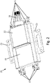
- the inverter 10 for a photovoltaic system in an exploded view.
- the inverter 10 comprises a substantially planar base plate 11, the rear side (in 1 not visible) forms an outer rear wall of the inverter 10.
- the base plate 11 has pedestals 12 which rise towards the front of the base plate.
- the inverter 10 includes a printed circuit board 13 which is mounted on the base plate 11 and includes electrical and electronic components which are set up to generate an alternating current from a direct current. Some of the components on the printed circuit board 13, for example semiconductor switches in an inverter bridge circuit or coils and chokes, generate losses during operation of the inverter 10, which are converted into heat and must be dissipated from inside the inverter 10.
- heat-generating components in particular the semiconductor switches, are mounted on the printed circuit board 13 in the area of the pedestal-shaped elevations 12 in such a way that there is thermal contact between the heat-generating components, while the rest of the printed circuit board, which is outside the areas of the pedestal-shaped elevations 12, does not having thermal contact with the base plate 11.
- the inverter 10 includes a cover 14 which is connected to the base plate 11 and in particular can rest on the base plate 11 .
- the space between the front side of the base plate 11 and the cover 14 can be completely filled with a casting compound (not shown here), the casting compound enclosing in particular the printed circuit board, i.e. both sides of the printed circuit board 13 are largely completely covered, possibly with the exception of the connecting surfaces between the circuit board 13 or the heat-generating components on it and the pedestal-like elevations 12 of the base plate 11.
- the base plate 11 and the cover 14 thus form a housing that essentially completely encloses at least the circuit board 13, this housing also completely enclosing the casting compound.
- a part of the housing, in particular a part of the cover 14 can also be surrounded by the casting compound, so that an outer surface of the inverter 10 is formed by the casting compound.
- the inverter 10 comprises direct current connections 15, which are provided in pairs, one connection in each connection pair being set up for connection to a positive pole and the other connection in each connection pair being set up for connection with a negative pole of a direct current source.
- the DC connections 15 are arranged on a lateral end surface of the housing in corresponding holes in the cover 14 and protrude into the housing in such a way that they are partially surrounded by the casting compound located between the base plate 11 and the cover 14, in particular by the DC connections 15 are partially and the electrical connections between the DC connections 15 and the circuit board 13 optionally completely cast in the potting compound.
- the inverter 10 includes an AC connection 16, which is also arranged on a lateral end face of the housing and extends through a hole 17 in the cover 14 into the casting compound, in particular by the AC connection 16 being at least partially cast into the casting compound.
- the AC connection 16 is provided for connecting the inverter 10 to an AC voltage network, the AC voltage connection 16 comprising electrical contacts 18 which are connected to the printed circuit board 13 and to which the individual conductors of the AC voltage network to be connected can be connected.
- connections of the inverter 10 in particular the DC connections 15 and AC connections 16 are not completely from the Potting compound are enclosed in order to have external access to these connections and to connect DC or AC lines to it.
- the AC voltage connection 16 can in particular be designed as a cable gland, with a threaded part of the cable gland protruding through the hole 17 in the cover from the housing and a counterpart of the cable gland can be screwed onto the threaded part from outside the housing.
- the inverter 10 can be designed in such a way that two pairs of the direct current connections 15 are connected in series or in parallel and in this respect are connected in pairs to a step-up converter arranged on the circuit board 13 which can in particular regulate a direct current voltage at the direct current connections 15 .
- FIG 2 shows a further embodiment of an inverter 20 for a photovoltaic system in a representation assembled and ready for operation.
- the inverter 20 in turn comprises DC connectors 15, which are arranged in pairs on the side end face of the case of the inverter 20, and an AC connector 16 on a side end face of the case of the inverter 20, the case of the inverter 20 according to FIG 2 is formed by a base plate (not visible), a cover 21 and a casting compound 22.
- the electrical and electronic components of the inverter 20 are analogous to those of the inverter 10 according to FIG 1 arranged on a printed circuit board, which is located under the cover 21 and inside the potting compound 22.
- the casting compound 22 also extends into an area between the cover 21 and the base plate and in particular also encloses the direct current connections 15 and the alternating current connection 16 at least partially. It is understood that the lid 21 according to 2 covers only a part of the casting compound 22, can also be designed in such a way that it covers the entire casting compound 22 and thus forms the entire surface of the inverter 20 opposite the base plate.
- the inverter 20 also has fastening lugs 23 which can be arranged on the cover 21 or on the base plate of the inverter 20 and protrude laterally beyond the casting compound 22 .
- the fastening tabs 23 have means for fastening the inverter 23 to a wall, a frame or directly to a photovoltaic module, with these means in 2 are formed, for example, as grooves for receiving screws.
- the inverter 20 includes a total of four pairs of direct current connections 15 to which a total of four individual photovoltaic modules or strings of photovoltaic modules can be connected. Two pairs of DC connections can be used 15 can be connected in series or in parallel with a step-up converter arranged on the printed circuit board inside the inverter 20 . Furthermore, the inverter 20 may include two boost converters connected in parallel with an inverter bridge circuit inside the inverter 20 .
- FIG 3 shows an embodiment of an inverter 30 for a photovoltaic system in a sectional view.
- the inverter 30 in turn comprises DC terminals 15, which are arranged in pairs on the side end surface of the housing of the inverter 30, and an AC terminal 16 on a side end surface of the housing of the inverter 30, the housing of the inverter 30 according to FIG 3 is formed by the base plate 11 and the cover 14.
- the space between the base plate 11 and the cover 14 can be completely filled with a casting compound (in 3 not visible).
- the electrical and electronic components of the inverter 30 are analogous to those of the inverters 10 and 20 according to FIG figs 1 and 2 arranged on a circuit board 13, which is located inside the potting compound.
- the printed circuit board 13 is mounted on the base plate 11, with heat-generating components of the inverter 30 being arranged on the printed circuit board 11 in such a way that they are in the area of the pedestal-shaped elevations 12 of the base plate 11 and are therefore in thermal contact with the base plate 11, resulting in good Dissipation of the heat generated by the components to the environment is guaranteed.
- a grid disconnection point in particular a grid disconnection relay, and/or at least one communication unit that is set up for power line communication via the DC connections 15 and/or the AC connection 16 can be arranged on the printed circuit board 13 .
Description
Die Erfindung betrifft einen Wechselrichter für eine Photovoltaikanlage.The invention relates to an inverter for a photovoltaic system.
Ein Wechselrichter für eine Photovoltaikanlage wandelt einen Gleichstrom eines gleichspannungsseitig angeschlossenen Photovoltaikgenerators in einen Wechselstrom und speist diesen Wechselstrom in ein wechselspannungsseitig an den Wechselrichter angeschlossenes Wechselspannungsnetz ein.An inverter for a photovoltaic system converts a direct current from a photovoltaic generator connected on the DC voltage side into an alternating current and feeds this alternating current into an AC voltage network connected to the inverter on the AC voltage side.
Dabei kann der Photovoltaikgenerator aus lediglich einem Photovoltaikmodul bestehen, das direkt an den Wechselrichter anschließbar ist, wobei der Wechselrichter gegebenenfalls auch direkt an das Photovoltaikmodul montiert oder zumindest in dessen Nähe angeordnet sein kann, insbesondere auf einem Hausdach, auf dem eine Vielzahl von Photovoltaikmodulen mit entsprechend jeweils zugeordneten Wechselrichtern angeordnet sein kann. Man spricht in diesem Fall aufgrund der vergleichsweise geringen elektrischen Leistung eines einzelnen Photovoltaikmoduls (deutlich kleiner als 1 kW) regelmäßig von einem Mikro-Wechselrichter. Ein Nachteil einer derart mit Mikro-Wechselrichtern aufgebauten Photovoltaikanlage besteht in der relativ aufwändigen Wechselstrom-Verkabelung, mit der die Wechselrichter untereinander und mit einem Netzanschlusspunkt des Wechselspannungsnetzes verbunden werden müssen.The photovoltaic generator can consist of just one photovoltaic module that can be connected directly to the inverter, in which case the inverter can also be mounted directly on the photovoltaic module or at least arranged in its vicinity, in particular on a house roof on which a large number of photovoltaic modules with corresponding respectively associated inverters can be arranged. In this case, due to the comparatively low electrical output of an individual photovoltaic module (significantly less than 1 kW), one regularly speaks of a micro-inverter. A disadvantage of a photovoltaic system constructed in this way with micro-inverters is the relatively complex AC cabling, with which the inverters must be connected to one another and to a grid connection point of the AC voltage grid.
Der Photovoltaikgenerator kann auch eine Vielzahl von Photovoltaikmodulen umfassen, die in Reihen- und/oder Parallelschaltung elektrisch miteinander verbunden sind und einen String bilden, wobei die Endpunkte dieses Strings mit gleichspannungsseitigen Anschlüssen eines Wechselrichter verbunden werden können, wie in
Je nach Anzahl der PhotovoltaiKmodule des Photovoltaikgenerators und damit der vom Wechselrichter umzuwandelnden elektrischen Leistung spricht man hier von String-Wechselrichter (etwa 1 kW bis ca. 100 kW) oder Zentral-Wechselrichter (größer etwa 100 kW). Dabei kann jeder String- bzw. Zentral-Wechselrichter mehrere gleichspannungsseitige Anschlüsse zum Anschluss mehrerer Strings umfassen. Ein Nachteil einer derart mit String- oder Zentral-Wechselrichtern aufgebauten Photovoltaikanlage besteht darin, dass die einzelnen Strings nur gemeinsam vom Wechselrichter gesteuert werden können, insbesondere hinsichtlich einer gemeinsamen Betriebsspannung des Strings und einem etwaigen Abschalten im Fehler- oder Gefahrenfall. Daher ist es in dieser Konfiguration einer Photovoltaikanlage nicht ohne weiteres möglich, die Betriebsspannung einzelner Photovoltaikmodule zu beeinflussen, um einen jeweils optimalen Arbeitspunkt einzustellen, der beispielsweise bei einer Verschattung von Teilen des Strings nicht über die vom Wechselrichter vorgegebene Stringspannung einstellbar ist.Depending on the number of photovoltaic modules in the photovoltaic generator and thus the electrical power to be converted by the inverter, we speak of string inverters (approx. 1 kW to approx. 100 kW) or central inverters (greater than approx. 100 kW). Each string or central inverter can include multiple connections on the DC voltage side for connecting multiple strings. A disadvantage of a photovoltaic system constructed in this way with string or central inverters is that the individual strings can only be controlled together by the inverter, particularly with regard to a common operating voltage of the string and any shutdown in the event of a fault or danger. It is therefore not readily possible in this configuration of a photovoltaic system influencing the operating voltage of individual photovoltaic modules in order to set an optimum operating point in each case, which cannot be set via the string voltage specified by the inverter, for example if parts of the string are in shadow.
Der Erfindung liegt die Aufgabe zugrunde, einen Wechselrichter bereitzustellen, der die Nachteile der bekannten Lösungen nicht aufweist und Vorteile hinsichtlich der Installation und des Betriebs einer Photovoltaikanlage bietet.The object of the invention is to provide an inverter that does not have the disadvantages of the known solutions and offers advantages with regard to the installation and operation of a photovoltaic system.
Die Aufgabe wird durch einen Wechselrichter mit den Merkmalen des Patentanspruchs 1 gelöst. Bevorzugte Ausführungsformen sind in den abhängigen Patentansprüchen definiert.The object is achieved by an inverter having the features of patent claim 1. Preferred embodiments are defined in the dependent claims.
Ein erfindungsgemäßer Wechselrichter für eine Photovoltaikanlage umfasst eine im Wesentlichen ebene Grundplatte mit einer Vorderseite und einer Rückseite, wobei die Rückseite eine äußere Rückwand des Wechselrichters bildet. Die Grundplatte weist mindestens eine podestförmige Erhöhung auf, die sich in Richtung der Vorderseite der Grundplatte erhebt. Weiterhin umfasst der Wechselrichter eine Leiterplatte mit wärmeerzeugenden Bauteilen, wobei die Leiterplatte auf der Grundplatte montiert ist. Dabei sind die wärmeerzeugenden Bauteile im Bereich der podestförmigen Erhöhung auf der Leiterplatte angeordnet und stehen mit der podestförmigen Erhöhung in thermischem Kontakt, so dass die von den Bauteilen erzeugte Wärme über die Grundplatte effektiv nach außen geführt wird.An inverter according to the invention for a photovoltaic system comprises an essentially flat base plate with a front and a rear, the rear forming an outer rear wall of the inverter. The base plate has at least one raised pedestal that rises towards the front of the base plate. Furthermore, the inverter includes a printed circuit board with heat-generating components, the printed circuit board being mounted on the base plate. The heat-generating components are arranged in the area of the pedestal elevation on the printed circuit board and are in thermal contact with the pedestal elevation, so that the heat generated by the components is effectively conducted to the outside via the base plate.
Weiterhin umfasst der Wechselrichter eine Vergussmasse, die einen Raum auf der Vorderseite der Grundplatte ausfüllt und die Leiterplatte umschließt, sowie einen Deckel, der auf der Vergussmasse angeordnet an die Grundplatte anschließt, so dass die Grundplatte und der Deckel in Verbindung mit nicht abgedeckten oder außenliegenden Teilen der Vergussmasse ein Gehäuse bilden. Das Gehäuse weist mindestens zwei seitliche Endflächen auf. Darüber hinaus umfasst der Wechselrichter vier Eckbereiche und genau acht Gleichstromanschlüsse, die paarweise zum jeweiligen Anschluss von Photovoltaikmodulen eines Photovoltaikgenerators eingerichtet, an mindestens zwei der seitlichen Endflächen des Gehäuses angeordnet und zumindest teilweise in die Vergussmasse eingegossen sind, wobei die acht Gleichstromanschlüsse in vier Paaren an den vier Eckbereichen des Wechselrichters angeordnet sind, so dass die Photovoltaikmodule um den Wechselrichter herum angeordnet werden können, einen Wechselstromanschluss, der an einer der seitlichen Endflächen des Gehäuses angeordnet ist, wobei elektrische Kontakte des Wechselstromanschlusses mit der Leiterplatte verbunden sind und aus der Vergussmasse herausragen.Furthermore, the inverter comprises a potting compound that fills a space on the front of the base plate and encloses the circuit board, and a cover that is arranged on the potting compound and connects to the base plate, so that the base plate and the cover are connected to uncovered or external parts the potting compound form a housing. The housing has at least two lateral end faces. In addition, the inverter includes four corner areas and exactly eight DC connections, which are set up in pairs for the respective connection of photovoltaic modules of a photovoltaic generator, are arranged on at least two of the lateral end faces of the housing and are at least partially cast into the casting compound, with the eight DC connections being connected in four pairs to the four corner areas of the inverter are arranged so that the photovoltaic modules can be arranged around the inverter, an AC connection, which is arranged on one of the lateral end surfaces of the housing, wherein electrical contacts of the AC connection are connected to the circuit board and from the potting compound protrude.
Ein derartiger Wechselrichter ist dazu eingerichtet, dass an jeweils einem Paar seiner Gleichstromanschlüsse ein Photovoltaikgenerator bestehend aus mindestens einem Photovoltaikmodul oder einem String aus mehreren Photovoltaikmodulen anschließbar ist. Bevorzugt kann der Wechselrichter derart ausgelegt sein, dass an jedes Paar seiner Gleichstromanschlüsse genau ein Photovoltaikmodul anschließbar ist, indem der Wechselrichter auf eine umzuwandelnde elektrische Leistung ausgelegt ist, die im Wesentlichen der Summe der maximalen Leistungen der anzuschließenden Photovoltaikmodule entspricht. Dies bedeutet einerseits, dass der Wechselrichter auf eine vergleichsweise kleine Leistung im Bereich einiger 100 Watt bis wenige Kilowatt ausgelegt und insofern sehr kompakt gebaut sein kann. Andererseits kann der Wechselrichter aufgrund seiner kompakten Bauform in unmittelbarer Nähe der anzuschließenden Photovoltaikmodule montiert werden, insbesondere direkt an einem Photovoltaikmodul oder an einem Gestell, auf dem die Photovoltaikmodule montiert sind. Dadurch kann die Länge von Gleichstromleitungen zwischen den Photovoltaikmodulen und dem Wechselrichter minimiert werden. Wenn an den Wechselrichter mindestens zwei Photovoltaikmodule angeschlossen werden, ergibt sich ein guter Kompromiss mit minimal kurzen Gleichstromleitungen und einer im Vergleich zu einem Aufbau mit bekannten Mikrowechselrichtern deutlich vereinfachten Wechselstromverkabelung. Dieser Vorteil kommt insbesondere bei einem Wechselrichter mit acht Gleichstromanschlüssen zum Anschluss von vier Photovoltaikmodulen zum Tragen, indem die Photovoltaikmodule um den Wechselrichter herum angeordnet werden, so dass der Wechselrichter im Bereich der Ecke, an der die vier Photovoltaikmodule zusammenstoßen, montiert werden kann und damit für alle vier Photovoltaikmodule einen Anschluss mit kurzen Anschlussleitungen erlaubt. Hierzu sind die acht Gleichstromanschlüsse in vier Paaren an den vier Eckbereichen des Wechselrichters angeordnet.Such an inverter is set up so that a photovoltaic generator consisting of at least one photovoltaic module or a string of several photovoltaic modules can be connected to one pair of its direct current connections. The inverter can preferably be designed in such a way that exactly one photovoltaic module can be connected to each pair of its direct current connections, in that the inverter is designed for an electrical power to be converted which essentially corresponds to the sum of the maximum powers of the photovoltaic modules to be connected. This means, on the one hand, that the inverter is designed for a comparatively small output in the range of a few 100 watts to a few kilowatts and can therefore be built very compactly. On the other hand, due to its compact design, the inverter can be mounted in the immediate vicinity of the photovoltaic modules to be connected, in particular directly on a photovoltaic module or on a frame on which the photovoltaic modules are mounted. As a result, the length of direct current lines between the photovoltaic modules and the inverter can be minimized. If at least two photovoltaic modules are connected to the inverter, a good compromise results with minimally short direct current lines and a significantly simplified alternating current cabling compared to a structure with known microinverters. This advantage is particularly evident in an inverter with eight DC connections for connecting four photovoltaic modules, by arranging the photovoltaic modules around the inverter so that the inverter can be mounted in the area of the corner where the four photovoltaic modules meet, and thus for all four photovoltaic modules can be connected with short connecting cables. For this purpose, the eight DC connections are arranged in four pairs at the four corner areas of the inverter.
Eine kompakte Bauform sowie eine einfache Montage des Wechselrichters ergeben sich zudem aus der geringen Anzahl benötigter Bauteile. Im einfachsten Fall kann eine vorgefertigte Leiterplatte auf der Grundplatte fixiert werden, der Deckel auf die Grundplatte gesetzt werden und abschließend der Raum zwischen Grundplatte und Deckel mit der Vergussmasse ausgefüllt werden. Die Gleichstrom- und Wechselstromanschlüsse können dabei bereits vor der Montage mit der Leiterplatte elektrisch verbunden sein.A compact design and simple installation of the inverter also result from the small number of components required. In the simplest case, a prefabricated printed circuit board can be fixed on the base plate, the cover can be placed on the base plate and the space between the base plate and cover can then be filled with the casting compound. The direct current and alternating current connections can already be electrically connected to the printed circuit board before assembly.
Durch die Verwendung der Vergussmasse ist es insbesondere nicht mehr notwendig, den Deckel derart mit der Grundplatte zu verbinden, dass ein hermetisch abgeschlossener Innenraum für die elektrischen und elektronischen Bauteile des Wechselrichters entsteht, in dem die elektrischen und elektronischen Bauteile des Wechselrichters vor äußeren Umgebungseinflüssen geschützt sind. Vielmehr schützt die Vergussmasse die elektrischen und elektronischen Bauteile des Wechselrichters bereits in einem ausreichenden Maße und sorgt gleichzeitig für eine verbesserte Entwärmung der Bauteile auf der Leiterplatte. Der Deckel des Wechselrichters kann zudem zusammen mit der Grundplatte eine Vergussform für die Vergussmasse darstellen, sodass die Vergussmasse direkt in den Raum zwischen Deckel und Grundplatte eingefüllt werden kann. Alternativ kann die Grundplatte mit der darauf montierten Leiterplatte und gegebenenfalls mit den Gleichstrom- und Wechselstromanschlüssen in einer separaten Vergussform mit der Vergussmasse vergossen und der Deckel nachträglich auf der Vergussmasse montiert werden. Sofern der Deckel aus einem elektrisch leitfähigen Material besteht oder mit einem solchen beschichtet ist, dient der Deckel zudem als elektromagnetische Abschirmung.By using the casting compound, it is in particular no longer necessary to connect the cover to the base plate in such a way that a hermetically sealed interior space is created for the electrical and electronic components of the inverter, in which the electrical and electronic components of the inverter are protected from external environmental influences . Rather, the potting compound protects the electrical and electronic components of the inverter to a sufficient degree and at the same time ensures improved cooling of the components on the printed circuit board. The lid of the inverter can also represent a casting mold for the casting compound together with the base plate, so that the casting compound can be filled directly into the space between the cover and the base plate. Alternatively, the base plate with the printed circuit board mounted on it and optionally with the direct current and alternating current connections can be cast in a separate casting mold with the casting compound and the cover can be subsequently mounted on the casting compound. If the cover consists of an electrically conductive material or is coated with such a material, the cover also serves as electromagnetic shielding.
Zur Montage des Wechselrichters an einem Photovoltaikmodul oder einem Gestell eines Photovoltaikgenerators kann der Wechselrichter eine Befestigungslasche aufweisen, die derart an dem Deckel oder an der Grundplatte des Wechselrichters angeordnet ist, dass sie seitlich über das Gehäuse des Wechselrichters hinaus ragt. Die Befestigungslasche kann dabei als Teil der Grundplatte oder des Deckels oder als ein separates Teil ausgebildet sein und Mittel zur Aufnahme von Befestigungsmitteln aufweisen, insbesondere Bohrungen oder Nuten zur Aufnahme von Schrauben, zum Verrasten mit korrespondierenden Raststrukturen, zum Einhängen in Haken oder ähnliches. Eine derartige Befestigungslasche kann zudem die Montage des Wechselrichters vereinfachen, indem der Wechselrichter während seiner Montage mittels der Befestigungslasche fixiert werden kann.To mount the inverter on a photovoltaic module or a frame of a photovoltaic generator, the inverter can have a fastening strap which is arranged on the cover or on the base plate of the inverter in such a way that it protrudes laterally beyond the housing of the inverter. The fastening tab can be designed as part of the base plate or the cover or as a separate part and have means for receiving fastening means, in particular bores or grooves for receiving screws, for latching with corresponding latching structures, for hanging in hooks or the like. A fastening strap of this type can also simplify the installation of the inverter, in that the inverter can be fixed in place by means of the fastening strap during installation.
Der Wechselstromanschluss des Wechselrichters kann als Kabelverschraubung ausgeführt sein. Eine Kabelverschraubung ermöglicht es, ein Wechselstromkabel, das mehrere Adern umfasst, auf einfache Weise mit den elektrischen Kontakten des Wechselstromanschlusses und damit mit der Leiterplatte zu verbinden, wobei diese Verbindung durch die Kabelverschraubung hinreichend dicht gegenüber der Umgebung ist.The AC connection of the inverter can be designed as a cable gland. A cable gland makes it possible to easily connect an AC cable, which comprises a plurality of wires, to the electrical contacts of the AC connection and thus to the printed circuit board, with this connection being sufficiently sealed with respect to the environment thanks to the cable gland.
In einer Ausführungsform des Wechselrichters können je zwei Paare von Gleichstromanschlüssen in Reihe oder parallel mit einem auf der Leiterplatte angeordneten Hochsetzsteller verbunden sein. Dadurch ist der Wechselrichter in der Lage, einen gemeinsamen Arbeitspunkt der an die Gleichstromanschlüsse angeschlossenen Photovoltaikmodul in einem weiten Spannungsbereich einzustellen.In one embodiment of the inverter, two pairs of direct current connections can be connected in series or in parallel to a step-up converter arranged on the printed circuit board. As a result, the inverter is able to set a common operating point for the photovoltaic modules connected to the DC connections over a wide voltage range.
Weiterhin kann der Wechselrichter mindestens zwei Hochsetzsteller umfassen, deren Ausgang gemeinsam elektrisch parallel geschaltet und mit einer auf der Leiterplatte angeordneten Wechselrichterbrückenschaltung verbunden ist. Dadurch ist der Wechselrichter in der Lage, mehrere an die Gleichstromanschlüsse angeschlossene Photovoltaikmodule unabhängig voneinander zu steuern sowie gegebenenfalls spannungsfrei zu schalten.Furthermore, the inverter can include at least two step-up converters, the output of which is electrically connected in parallel and connected to an inverter bridge circuit arranged on the printed circuit board. As a result, the inverter is able to control several photovoltaic modules connected to the DC connections independently of one another and, if necessary, to switch them off.
Aufgrund der kompakten Bauweise des Wechselrichters können weitere Bauteile im Wechselrichter, d.h. im Gehäuse bzw. in der Vergussmasse des Wechselrichters angeordnet werden. Insbesondere kann auf der Leiterplatte eine Netztrennstelle angeordnet sein, die mindestens ein Relais umfasst. Zusätzlich kann der Wechselrichter eine Kommunikationseinheit umfassen, die zur Powerline-Kommunikation über die Gleichstromanschlüsse und/oder den Wechselstromanschluss eingerichtet ist.Due to the compact design of the inverter, further components can be arranged in the inverter, i.e. in the housing or in the potting compound of the inverter. In particular, a mains disconnection point can be arranged on the printed circuit board, which includes at least one relay. In addition, the inverter can include a communication unit that is set up for power line communication via the DC connections and/or the AC connection.
Im Folgenden wird die Erfindung anhand in den Figuren dargestellter Ausführungsbeispiele weiter erläutert und beschrieben.
- Fig. 1
- zeigt eine Ausführungsform des erfindungsgemäßen Wechselrichters in einer Explosionsdarstellung,
- Fig. 2
- zeigt eine weitere Ausführungsform des erfindungsgemäßen Wechselrichters in einem montiert Zustand, und
- Fig. 3
- zeigt eine weitere Ausführungsform des erfindungsgemäßen Wechselrichters in einer Schnittdarstellung.
- 1
- shows an embodiment of the inverter according to the invention in an exploded view,
- 2
- shows a further embodiment of the inverter according to the invention in an assembled state, and
- 3
- shows a further embodiment of the inverter according to the invention in a sectional view.
Weiterhin umfasst der Wechselrichter 10 einen Deckel 14, der an die Grundplatte 11 anschließt ist und insbesondere auf der Grundplatte 11 aufliegen kann. Der Raum zwischen der Vorderseite der Grundplatte 11 und dem Deckel 14 kann vollständig mit einer Vergussmasse ausgefüllt sein (hier nicht dargestellt), wobei die Vergussmasse insbesondere die Leiterplatte umschließt, d.h. beide Seiten der Leiterplatte 13 weitgehend vollständig bedeckt, ggf. mit Ausnahme der Verbindungsflächen zwischen der Leiterplatte 13 bzw. den wärmeerzeugenden Bauteilen darauf und den podestförmigen Erhöhungen 12 der Grundplatte 11. Die Grundplatte 11 und der Deckel 14 bilden somit ein zumindest die Leiterplatte 13 im Wesentlichen vollständig umschließendes Gehäuse, wobei dieses Gehäuse auch die Vergussmasse vollständig umschließt. Alternativ oder zusätzlich kann ein Teil des Gehäuses, insbesondere ein Teil des Deckels 14 ebenfalls von der Vergussmasse umschlossen sein, so dass eine Außenfläche des Wechselrichters 10 von der Vergussmasse gebildet wird.Furthermore, the
Weiterhin umfasst der Wechselrichter 10 Gleichstromanschlüsse 15, die paarweise vorgesehen sind, wobei je ein Anschluss eines Anschlusspaares zur Verbindung mit einem positiven Pol und der jeweils andere Anschluss eines Anschlusspaares zur Verbindung mit einem negativen Pol einer Gleichstromquelle eingerichtet sind. Die Gleichstromanschlüsse 15 sind in einem zusammengebauten Zustand des Wechselrichters 10 an einer seitlichen Endfläche des Gehäuses in entsprechenden Löchern im Deckel 14 angeordnet und ragen derart in das Gehäuse, dass sie von der zwischen Grundplatte 11 und Deckel 14 befindlichen Vergussmasse teilweise umschlossen sind, insbesondere indem die Gleichstromanschlüsse 15 teilweise und die elektrische Verbindungen zwischen den Gleichstromanschlüssen 15 und der Leiterplatte 13 gegebenenfalls komplett in die Vergussmasse eingegossen sind.Furthermore, the
Weiterhin umfasst der Wechselrichter 10 einen Wechselstromanschluss 16, der ebenfalls an einer seitlichen Endfläche des Gehäuses angeordnet ist und durch ein Loch 17 im Deckel 14 in die Vergussmasse erstreckt, insbesondere indem der Wechselstromanschluss 16 zumindest teilweise in die Vergussmasse eingegossen ist. Der Wechselstromanschluss 16 ist zur Verbindung des Wechselrichter 10 mit einem Wechselspannungsnetz vorgesehen, wobei der Wechselspannungsanschluss 16 elektrische Kontakte 18 umfasst, die mit der Leiterplatte 13 verbunden sind und an die einzelne Leiter des anzuschließenden Wechselspannungsnetzes anschließbar sind.Furthermore, the
Es versteht sich, dass die Anschlüsse des Wechselrichters 10, insbesondere die Gleichstromanschlüsse 15 und Wechselstromanschlüsse 16 nicht vollständig von der Vergussmasse umschlossen sind, um von außen Zugriff auf diese Anschlüsse zu haben und Gleichstrom- bzw. Wechselstromleitungen daran anschließen zu können.It is understood that the connections of the
Der Wechselspannungsanschluss 16 kann insbesondere als Kabelverschraubung ausgeführt sein, wobei ein Gewindeteil der Kabelverschraubung durch das Loch 17 im Deckel aus dem Gehäuse herausragt und ein Gegenstück der Kabelverschraubung von außerhalb des Gehäuses auf den Gewindeteil aufgeschraubt werden kann.The
Der Wechselrichter 10 kann derart ausgeführt sein, dass je zwei Paare der Gleichstromanschlüsse 15 in Reihe oder parallel geschaltet und insofern paarweise mit einem auf der Leiterplatte 13 angeordneten Hochsetzsteller verbunden sind, der insbesondere eine Gleichstromspannung an den Gleichstromanschlüsse 15 regeln kann.The
Der Wechselrichter 20 weist weiterhin Befestigungslaschen 23 auf, die an dem Deckel 21 oder an der Grundplatte des Wechselrichters 20 angeordnet sein können und seitlich über die Vergussmasse 22 hinausragen. Die Befestigungslaschen 23 weisen Mittel zu Befestigung des Wechselrichter 23 an einer Wand, einem Gestell oder auch direkt an einem Photovoltaikmodul auf, wobei diese Mittel in
Der Wechselrichter 20 umfasst insgesamt vier Paare von Gleichstromanschlüssen 15, an die insgesamt vier einzelne Photovoltaikmodule oder Strings aus Photovoltaikmodulen angeschlossen werden können. Dabei können je zwei Paare von Gleichstromanschlüssen 15 in Reihe oder parallel mit je einem auf der Leiterplatte innerhalb des Wechselrichters 20 angeordneten Hochsetzsteller verbunden sein. Weiterhin kann der Wechselrichter 20 zwei Hochsetzsteller umfassen, die parallel mit einer Wechselrichterbrückenschaltung im Inneren des Wechselrichters 20 verbunden sind.The
Darüber hinaus können auf der Leiterplatte 13 eine Netztrennstelle, insbesondere ein Netztrennrelais, und/oder mindestens eine Kommunikationseinheit, die zur Powerline-Kommunikation über die Gleichstromanschlüsse 15 und/oder den Wechselstromanschluss 16 eingerichtet ist, angeordnet sein. Dies gilt selbstverständlich für alle dargestellte Wechselrichter 10, 20, 30 gemäß der
- 10, 20, 30 Wechselrichter10, 20, 30 inverters
- 11 Grundplatte11 base plate
- 12 Erhöhungen12 raises
- 13 Leiterplatte13 circuit board
- 14 Deckel14 lids
- 15 Gleichstromanschluss15 DC connector
- 16 Wechselstromanschluss16 AC power connector
- 17 Loch17 holes
- 18 Kontakt18 contact
- 21 Deckel21 cover
- 22 Vergussmasse22 potting compound
- 23 Befestigungslasche23 fastening tab
Claims (7)
- An inverter (20) for a photovoltaic system, comprising:- a substantially planar base plate (11) having a front side and a rear side, the rear side forming an outer rear wall of the inverter (20), and having at least one pedestal-shaped elevation (12) rising towards the front side of the base plate (11),- a printed circuit board (13) with heat-generating components, the printed circuit board (13) being mounted on the base plate (11) in such a way that the heat-generating components are arranged on the printed circuit board (13) in the region of the pedestal-shaped elevation (12) and are in thermal contact with the pedestal-shaped elevation (12),- a potting compound (22) which fills a space on the front side of the base plate (11) and encloses the printed circuit board (13)- a cover (21) which is arranged on the potting compound (22), adjoins the base plate (11) and partially encloses the potting compound (22), so that the base plate (11) and the cover (21), in conjunction with uncovered parts of the potting compound (22), form a housing, the housing having at least two lateral end surfaces,- four corner areas,- exactly eight DC terminals (15), arranged in pairs for the respective connection of photovoltaic modules of a photovoltaic generator, arranged on at least two of the lateral end faces of the housing and at least partially encapsulated in the potting compound (22), the eight DC terminals being arranged in four pairs on the four corner regions of the inverter, so that the photovoltaic modules can be arranged around the inverter,- an AC terminal (16) arranged on one of the lateral end faces of the housing, electrical contacts (18) of the AC terminal (16) being connected to the circuit board (13) and protruding from the potting compound (22).
- The inverter (20) according to claim 1, wherein at least one fastening lug (23) is arranged on the cover (21) or on the base plate (11) in such a way that it protrudes laterally beyond the housing of the inverter (20), the fastening lug (23) having means for receiving fastening means.
- The inverter (20) according to claim 1 or 2, wherein the AC connection (16) is designed as a cable gland.
- The inverter (20) according to one of the preceding claims, wherein two pairs each of DC terminals (15) are connected in series or in parallel to a step-up converter arranged on the printed circuit board (13).
- The inverter (20) according to any one of the preceding claims, comprising at least two boost converters whose output is electrically connected in parallel with each other and connected to an inverter bridge circuit arranged on the printed circuit board (13).
- The inverter (20) according to any one of the preceding claims, comprising a mains disconnection point arranged on the printed circuit board (13).
- The inverter (20) according to any one of the preceding claims, comprising at least one communication unit arranged for powerline communication via the DC terminals (15) and/or the AC terminal (16).
Applications Claiming Priority (2)
| Application Number | Priority Date | Filing Date | Title |
|---|---|---|---|
| DE202017107643.1U DE202017107643U1 (en) | 2017-12-15 | 2017-12-15 | inverter |
| PCT/EP2018/084025 WO2019115403A1 (en) | 2017-12-15 | 2018-12-07 | Inverter |
Publications (2)
| Publication Number | Publication Date |
|---|---|
| EP3724981A1 EP3724981A1 (en) | 2020-10-21 |
| EP3724981B1 true EP3724981B1 (en) | 2022-04-06 |
Family
ID=61082655
Family Applications (1)
| Application Number | Title | Priority Date | Filing Date |
|---|---|---|---|
| EP18815688.9A Active EP3724981B1 (en) | 2017-12-15 | 2018-12-07 | Inverter |
Country Status (5)
| Country | Link |
|---|---|
| US (1) | US11522494B2 (en) |
| EP (1) | EP3724981B1 (en) |
| CN (1) | CN111466074B (en) |
| DE (1) | DE202017107643U1 (en) |
| WO (1) | WO2019115403A1 (en) |
Families Citing this family (3)
| Publication number | Priority date | Publication date | Assignee | Title |
|---|---|---|---|---|
| USD930584S1 (en) * | 2019-05-14 | 2021-09-14 | Vertiv Tech Co., Ltd. | Rectifier |
| IT202100011054A1 (en) * | 2021-04-30 | 2022-10-30 | Hdemia S R L | PHOTOVOLTAIC MASTER-SLAVE SYSTEM |
| CN117154830A (en) * | 2023-10-24 | 2023-12-01 | 宁波德业变频技术有限公司 | Integration of photovoltaic grid-connected inverter and photovoltaic module |
Family Cites Families (16)
| Publication number | Priority date | Publication date | Assignee | Title |
|---|---|---|---|---|
| US6362964B1 (en) * | 1999-11-17 | 2002-03-26 | International Rectifier Corp. | Flexible power assembly |
| JP2003332526A (en) * | 2001-11-07 | 2003-11-21 | Hitachi Ltd | Power conversion apparatus |
| US7505294B2 (en) * | 2003-05-16 | 2009-03-17 | Continental Automotive Systems Us, Inc. | Tri-level inverter |
| JP4644275B2 (en) * | 2008-07-29 | 2011-03-02 | 日立オートモティブシステムズ株式会社 | Power converter and electric vehicle |
| DE102008052348B4 (en) * | 2008-10-20 | 2016-12-29 | Te Connectivity Germany Gmbh | Connecting device for connecting an electrical conductor with a solar module, and solar module with such a connection device |
| JP5740986B2 (en) * | 2010-03-17 | 2015-07-01 | 株式会社安川電機 | Power converter |
| JP5504219B2 (en) * | 2011-07-27 | 2014-05-28 | 日立オートモティブシステムズ株式会社 | Power converter |
| US8811015B2 (en) * | 2012-02-16 | 2014-08-19 | Mission Motor Company | Motor control device |
| US9735699B2 (en) * | 2014-01-15 | 2017-08-15 | Lg Electronics Inc. | Integral inverter and solar cell module including the same |
| KR102298674B1 (en) * | 2014-01-28 | 2021-09-03 | 엘지전자 주식회사 | Solar cell module and photovoltaic power generation system including the same |
| KR102193871B1 (en) * | 2014-01-28 | 2020-12-22 | 엘지전자 주식회사 | Integral inverter and solar cell module including the same |
| DE102014105985A1 (en) | 2014-04-29 | 2015-10-29 | Sma Solar Technology Ag | Converter module for converting electrical power and inverters for a photovoltaic system with at least two converter modules |
| KR102206389B1 (en) * | 2014-12-08 | 2021-01-22 | 엘에스일렉트릭(주) | Photovoltaic inverter stack |
| JP6278243B2 (en) * | 2015-01-07 | 2018-02-14 | 株式会社オートネットワーク技術研究所 | Power storage unit |
| CN106230288A (en) * | 2016-08-08 | 2016-12-14 | 湖州新智源电子科技有限公司 | A kind of multichannel MPPT Miniature inverter and control method thereof |
| KR20170034781A (en) * | 2016-10-21 | 2017-03-29 | 동양이엔피 주식회사 | Mutiple input photovoltaic inverter apparatus |
-
2017
- 2017-12-15 DE DE202017107643.1U patent/DE202017107643U1/en active Active
-
2018
- 2018-12-07 CN CN201880076882.6A patent/CN111466074B/en active Active
- 2018-12-07 EP EP18815688.9A patent/EP3724981B1/en active Active
- 2018-12-07 WO PCT/EP2018/084025 patent/WO2019115403A1/en unknown
-
2020
- 2020-06-15 US US16/901,179 patent/US11522494B2/en active Active
Also Published As
| Publication number | Publication date |
|---|---|
| WO2019115403A1 (en) | 2019-06-20 |
| CN111466074B (en) | 2024-02-27 |
| US11522494B2 (en) | 2022-12-06 |
| EP3724981A1 (en) | 2020-10-21 |
| DE202017107643U1 (en) | 2018-01-11 |
| US20200313607A1 (en) | 2020-10-01 |
| CN111466074A (en) | 2020-07-28 |
Similar Documents
| Publication | Publication Date | Title |
|---|---|---|
| EP3724981B1 (en) | Inverter | |
| EP3351072B1 (en) | Inverter for transforming direct current into alternating current | |
| EP2954613B1 (en) | Filter component | |
| DE102013112110A1 (en) | Functional component shell for a component assembly system | |
| EP2996449B1 (en) | Frequency converter assembly with a multiphase frequency converter | |
| DE202011005667U1 (en) | Compact busbar arrangement, switching device and power distribution system | |
| EP2905888A1 (en) | Inverter | |
| EP2302782A1 (en) | Frequency converter assembly | |
| DE102016108562A1 (en) | SEMICONDUCTOR COMPONENT WITH STACKED CONNECTORS | |
| DE102014010067A1 (en) | Voltage protected manufacturable motor vehicle battery | |
| DE112018000388T5 (en) | POWER CONVERTER | |
| DE202021103872U1 (en) | photovoltaic power conversion device | |
| DE19618736A1 (en) | Terminal block and control unit with terminal block | |
| DE202018103164U1 (en) | Electrical or electronic device comprising a housing with two electromagnetically shielded areas | |
| DE102014110346A1 (en) | Compact structure of a power supply device that can minimize electromagnetic noise | |
| DE102019133377A1 (en) | INVERTER WITH COMPACT DESIGN | |
| DE102019120031A1 (en) | Control device | |
| EP0618763B1 (en) | Shielded casing for electric elements with plug for internal and external cable connection | |
| DE112016000036T5 (en) | Connection structure of a power semiconductor module | |
| EP2505050B1 (en) | Housing system | |
| DE7505830U (en) | DEVICE FOR HIGH-VOLTAGE-PROOF AND GOOD THERMAL CONDUCTING INSTALLATION OF SEMICONDUCTOR COMPONENTS | |
| DE102016014530B4 (en) | Electrical power distribution | |
| DE112019002391T5 (en) | PERFORMANCE CONVERSION DEVICE | |
| WO2014161828A1 (en) | Inverter and direct-current connection unit for an inverter | |
| DE102022204199B3 (en) | Electronics module with self-clamping and electrically contacting housing cover |
Legal Events
| Date | Code | Title | Description |
|---|---|---|---|
| STAA | Information on the status of an ep patent application or granted ep patent |
Free format text: STATUS: UNKNOWN |
|
| STAA | Information on the status of an ep patent application or granted ep patent |
Free format text: STATUS: THE INTERNATIONAL PUBLICATION HAS BEEN MADE |
|
| PUAI | Public reference made under article 153(3) epc to a published international application that has entered the european phase |
Free format text: ORIGINAL CODE: 0009012 |
|
| STAA | Information on the status of an ep patent application or granted ep patent |
Free format text: STATUS: REQUEST FOR EXAMINATION WAS MADE |
|
| 17P | Request for examination filed |
Effective date: 20200706 |
|
| AK | Designated contracting states |
Kind code of ref document: A1 Designated state(s): AL AT BE BG CH CY CZ DE DK EE ES FI FR GB GR HR HU IE IS IT LI LT LU LV MC MK MT NL NO PL PT RO RS SE SI SK SM TR |
|
| AX | Request for extension of the european patent |
Extension state: BA ME |
|
| DAV | Request for validation of the european patent (deleted) | ||
| DAX | Request for extension of the european patent (deleted) | ||
| GRAP | Despatch of communication of intention to grant a patent |
Free format text: ORIGINAL CODE: EPIDOSNIGR1 |
|
| STAA | Information on the status of an ep patent application or granted ep patent |
Free format text: STATUS: GRANT OF PATENT IS INTENDED |
|
| INTG | Intention to grant announced |
Effective date: 20211019 |
|
| GRAS | Grant fee paid |
Free format text: ORIGINAL CODE: EPIDOSNIGR3 |
|
| GRAA | (expected) grant |
Free format text: ORIGINAL CODE: 0009210 |
|
| STAA | Information on the status of an ep patent application or granted ep patent |
Free format text: STATUS: THE PATENT HAS BEEN GRANTED |
|
| AK | Designated contracting states |
Kind code of ref document: B1 Designated state(s): AL AT BE BG CH CY CZ DE DK EE ES FI FR GB GR HR HU IE IS IT LI LT LU LV MC MK MT NL NO PL PT RO RS SE SI SK SM TR |
|
| REG | Reference to a national code |
Ref country code: GB Ref legal event code: FG4D Free format text: NOT ENGLISH |
|
| RIN1 | Information on inventor provided before grant (corrected) |
Inventor name: MOESER, EPHRAIM Inventor name: WAPPLER, THOMAS Inventor name: KOTTHAUS, MICHAEL Inventor name: FRIEBE, JENS Inventor name: SOEDERBERG, TORSTEN Inventor name: BUCHHOLD, STEFAN |
|
| REG | Reference to a national code |
Ref country code: CH Ref legal event code: EP |
|
| REG | Reference to a national code |
Ref country code: AT Ref legal event code: REF Ref document number: 1482321 Country of ref document: AT Kind code of ref document: T Effective date: 20220415 |
|
| REG | Reference to a national code |
Ref country code: DE Ref legal event code: R096 Ref document number: 502018009360 Country of ref document: DE |
|
| REG | Reference to a national code |
Ref country code: IE Ref legal event code: FG4D Free format text: LANGUAGE OF EP DOCUMENT: GERMAN |
|
| REG | Reference to a national code |
Ref country code: NL Ref legal event code: FP |
|
| REG | Reference to a national code |
Ref country code: LT Ref legal event code: MG9D |
|
| PG25 | Lapsed in a contracting state [announced via postgrant information from national office to epo] |
Ref country code: SE Free format text: LAPSE BECAUSE OF FAILURE TO SUBMIT A TRANSLATION OF THE DESCRIPTION OR TO PAY THE FEE WITHIN THE PRESCRIBED TIME-LIMIT Effective date: 20220406 Ref country code: PT Free format text: LAPSE BECAUSE OF FAILURE TO SUBMIT A TRANSLATION OF THE DESCRIPTION OR TO PAY THE FEE WITHIN THE PRESCRIBED TIME-LIMIT Effective date: 20220808 Ref country code: NO Free format text: LAPSE BECAUSE OF FAILURE TO SUBMIT A TRANSLATION OF THE DESCRIPTION OR TO PAY THE FEE WITHIN THE PRESCRIBED TIME-LIMIT Effective date: 20220706 Ref country code: LT Free format text: LAPSE BECAUSE OF FAILURE TO SUBMIT A TRANSLATION OF THE DESCRIPTION OR TO PAY THE FEE WITHIN THE PRESCRIBED TIME-LIMIT Effective date: 20220406 Ref country code: HR Free format text: LAPSE BECAUSE OF FAILURE TO SUBMIT A TRANSLATION OF THE DESCRIPTION OR TO PAY THE FEE WITHIN THE PRESCRIBED TIME-LIMIT Effective date: 20220406 Ref country code: GR Free format text: LAPSE BECAUSE OF FAILURE TO SUBMIT A TRANSLATION OF THE DESCRIPTION OR TO PAY THE FEE WITHIN THE PRESCRIBED TIME-LIMIT Effective date: 20220707 Ref country code: FI Free format text: LAPSE BECAUSE OF FAILURE TO SUBMIT A TRANSLATION OF THE DESCRIPTION OR TO PAY THE FEE WITHIN THE PRESCRIBED TIME-LIMIT Effective date: 20220406 Ref country code: ES Free format text: LAPSE BECAUSE OF FAILURE TO SUBMIT A TRANSLATION OF THE DESCRIPTION OR TO PAY THE FEE WITHIN THE PRESCRIBED TIME-LIMIT Effective date: 20220406 Ref country code: BG Free format text: LAPSE BECAUSE OF FAILURE TO SUBMIT A TRANSLATION OF THE DESCRIPTION OR TO PAY THE FEE WITHIN THE PRESCRIBED TIME-LIMIT Effective date: 20220706 |
|
| PG25 | Lapsed in a contracting state [announced via postgrant information from national office to epo] |
Ref country code: RS Free format text: LAPSE BECAUSE OF FAILURE TO SUBMIT A TRANSLATION OF THE DESCRIPTION OR TO PAY THE FEE WITHIN THE PRESCRIBED TIME-LIMIT Effective date: 20220406 Ref country code: PL Free format text: LAPSE BECAUSE OF FAILURE TO SUBMIT A TRANSLATION OF THE DESCRIPTION OR TO PAY THE FEE WITHIN THE PRESCRIBED TIME-LIMIT Effective date: 20220406 Ref country code: LV Free format text: LAPSE BECAUSE OF FAILURE TO SUBMIT A TRANSLATION OF THE DESCRIPTION OR TO PAY THE FEE WITHIN THE PRESCRIBED TIME-LIMIT Effective date: 20220406 Ref country code: IS Free format text: LAPSE BECAUSE OF FAILURE TO SUBMIT A TRANSLATION OF THE DESCRIPTION OR TO PAY THE FEE WITHIN THE PRESCRIBED TIME-LIMIT Effective date: 20220806 |
|
| REG | Reference to a national code |
Ref country code: DE Ref legal event code: R097 Ref document number: 502018009360 Country of ref document: DE |
|
| PG25 | Lapsed in a contracting state [announced via postgrant information from national office to epo] |
Ref country code: SM Free format text: LAPSE BECAUSE OF FAILURE TO SUBMIT A TRANSLATION OF THE DESCRIPTION OR TO PAY THE FEE WITHIN THE PRESCRIBED TIME-LIMIT Effective date: 20220406 Ref country code: SK Free format text: LAPSE BECAUSE OF FAILURE TO SUBMIT A TRANSLATION OF THE DESCRIPTION OR TO PAY THE FEE WITHIN THE PRESCRIBED TIME-LIMIT Effective date: 20220406 Ref country code: RO Free format text: LAPSE BECAUSE OF FAILURE TO SUBMIT A TRANSLATION OF THE DESCRIPTION OR TO PAY THE FEE WITHIN THE PRESCRIBED TIME-LIMIT Effective date: 20220406 Ref country code: EE Free format text: LAPSE BECAUSE OF FAILURE TO SUBMIT A TRANSLATION OF THE DESCRIPTION OR TO PAY THE FEE WITHIN THE PRESCRIBED TIME-LIMIT Effective date: 20220406 Ref country code: DK Free format text: LAPSE BECAUSE OF FAILURE TO SUBMIT A TRANSLATION OF THE DESCRIPTION OR TO PAY THE FEE WITHIN THE PRESCRIBED TIME-LIMIT Effective date: 20220406 Ref country code: CZ Free format text: LAPSE BECAUSE OF FAILURE TO SUBMIT A TRANSLATION OF THE DESCRIPTION OR TO PAY THE FEE WITHIN THE PRESCRIBED TIME-LIMIT Effective date: 20220406 |
|
| PLBE | No opposition filed within time limit |
Free format text: ORIGINAL CODE: 0009261 |
|
| STAA | Information on the status of an ep patent application or granted ep patent |
Free format text: STATUS: NO OPPOSITION FILED WITHIN TIME LIMIT |
|
| PGFP | Annual fee paid to national office [announced via postgrant information from national office to epo] |
Ref country code: BE Payment date: 20221220 Year of fee payment: 5 |
|
| 26N | No opposition filed |
Effective date: 20230110 |
|
| PG25 | Lapsed in a contracting state [announced via postgrant information from national office to epo] |
Ref country code: AL Free format text: LAPSE BECAUSE OF FAILURE TO SUBMIT A TRANSLATION OF THE DESCRIPTION OR TO PAY THE FEE WITHIN THE PRESCRIBED TIME-LIMIT Effective date: 20220406 |
|
| PG25 | Lapsed in a contracting state [announced via postgrant information from national office to epo] |
Ref country code: SI Free format text: LAPSE BECAUSE OF FAILURE TO SUBMIT A TRANSLATION OF THE DESCRIPTION OR TO PAY THE FEE WITHIN THE PRESCRIBED TIME-LIMIT Effective date: 20220406 |
|
| REG | Reference to a national code |
Ref country code: CH Ref legal event code: PL |
|
| PG25 | Lapsed in a contracting state [announced via postgrant information from national office to epo] |
Ref country code: LU Free format text: LAPSE BECAUSE OF NON-PAYMENT OF DUE FEES Effective date: 20221207 |
|
| PG25 | Lapsed in a contracting state [announced via postgrant information from national office to epo] |
Ref country code: LI Free format text: LAPSE BECAUSE OF NON-PAYMENT OF DUE FEES Effective date: 20221231 Ref country code: IE Free format text: LAPSE BECAUSE OF NON-PAYMENT OF DUE FEES Effective date: 20221207 Ref country code: CH Free format text: LAPSE BECAUSE OF NON-PAYMENT OF DUE FEES Effective date: 20221231 |
|
| PGFP | Annual fee paid to national office [announced via postgrant information from national office to epo] |
Ref country code: GB Payment date: 20231220 Year of fee payment: 6 |
|
| PG25 | Lapsed in a contracting state [announced via postgrant information from national office to epo] |
Ref country code: IT Free format text: LAPSE BECAUSE OF FAILURE TO SUBMIT A TRANSLATION OF THE DESCRIPTION OR TO PAY THE FEE WITHIN THE PRESCRIBED TIME-LIMIT Effective date: 20220406 |
|
| PGFP | Annual fee paid to national office [announced via postgrant information from national office to epo] |
Ref country code: NL Payment date: 20231219 Year of fee payment: 6 Ref country code: FR Payment date: 20231219 Year of fee payment: 6 Ref country code: DE Payment date: 20231214 Year of fee payment: 6 |
|
| PGFP | Annual fee paid to national office [announced via postgrant information from national office to epo] |
Ref country code: BE Payment date: 20231218 Year of fee payment: 6 |