EP3724772B1 - Home agent based cache transfer acceleration scheme - Google Patents
Home agent based cache transfer acceleration scheme Download PDFInfo
- Publication number
- EP3724772B1 EP3724772B1 EP18783262.1A EP18783262A EP3724772B1 EP 3724772 B1 EP3724772 B1 EP 3724772B1 EP 18783262 A EP18783262 A EP 18783262A EP 3724772 B1 EP3724772 B1 EP 3724772B1
- Authority
- EP
- European Patent Office
- Prior art keywords
- probe
- cache
- entry
- early
- region
- Prior art date
- Legal status (The legal status is an assumption and is not a legal conclusion. Google has not performed a legal analysis and makes no representation as to the accuracy of the status listed.)
- Active
Links
Images

Classifications
-
- G—PHYSICS
- G06—COMPUTING OR CALCULATING; COUNTING
- G06F—ELECTRIC DIGITAL DATA PROCESSING
- G06F12/00—Accessing, addressing or allocating within memory systems or architectures
- G06F12/02—Addressing or allocation; Relocation
- G06F12/08—Addressing or allocation; Relocation in hierarchically structured memory systems, e.g. virtual memory systems
- G06F12/12—Replacement control
- G06F12/121—Replacement control using replacement algorithms
- G06F12/128—Replacement control using replacement algorithms adapted to multidimensional cache systems, e.g. set-associative, multicache, multiset or multilevel
-
- G—PHYSICS
- G06—COMPUTING OR CALCULATING; COUNTING
- G06F—ELECTRIC DIGITAL DATA PROCESSING
- G06F12/00—Accessing, addressing or allocating within memory systems or architectures
- G06F12/02—Addressing or allocation; Relocation
- G06F12/08—Addressing or allocation; Relocation in hierarchically structured memory systems, e.g. virtual memory systems
- G06F12/0802—Addressing of a memory level in which the access to the desired data or data block requires associative addressing means, e.g. caches
- G06F12/0806—Multiuser, multiprocessor or multiprocessing cache systems
- G06F12/0815—Cache consistency protocols
- G06F12/0817—Cache consistency protocols using directory methods
- G06F12/082—Associative directories
-
- G—PHYSICS
- G06—COMPUTING OR CALCULATING; COUNTING
- G06F—ELECTRIC DIGITAL DATA PROCESSING
- G06F12/00—Accessing, addressing or allocating within memory systems or architectures
- G06F12/02—Addressing or allocation; Relocation
- G06F12/08—Addressing or allocation; Relocation in hierarchically structured memory systems, e.g. virtual memory systems
- G06F12/0802—Addressing of a memory level in which the access to the desired data or data block requires associative addressing means, e.g. caches
- G06F12/0806—Multiuser, multiprocessor or multiprocessing cache systems
- G06F12/0815—Cache consistency protocols
- G06F12/0817—Cache consistency protocols using directory methods
- G06F12/0824—Distributed directories, e.g. linked lists of caches
-
- G—PHYSICS
- G06—COMPUTING OR CALCULATING; COUNTING
- G06F—ELECTRIC DIGITAL DATA PROCESSING
- G06F12/00—Accessing, addressing or allocating within memory systems or architectures
- G06F12/02—Addressing or allocation; Relocation
- G06F12/08—Addressing or allocation; Relocation in hierarchically structured memory systems, e.g. virtual memory systems
- G06F12/0802—Addressing of a memory level in which the access to the desired data or data block requires associative addressing means, e.g. caches
- G06F12/0806—Multiuser, multiprocessor or multiprocessing cache systems
- G06F12/0815—Cache consistency protocols
- G06F12/0817—Cache consistency protocols using directory methods
- G06F12/0826—Limited pointers directories; State-only directories without pointers
-
- G—PHYSICS
- G06—COMPUTING OR CALCULATING; COUNTING
- G06F—ELECTRIC DIGITAL DATA PROCESSING
- G06F12/00—Accessing, addressing or allocating within memory systems or architectures
- G06F12/02—Addressing or allocation; Relocation
- G06F12/08—Addressing or allocation; Relocation in hierarchically structured memory systems, e.g. virtual memory systems
- G06F12/0802—Addressing of a memory level in which the access to the desired data or data block requires associative addressing means, e.g. caches
- G06F12/0806—Multiuser, multiprocessor or multiprocessing cache systems
- G06F12/0815—Cache consistency protocols
- G06F12/0831—Cache consistency protocols using a bus scheme, e.g. with bus monitoring or watching means
- G06F12/0833—Cache consistency protocols using a bus scheme, e.g. with bus monitoring or watching means in combination with broadcast means (e.g. for invalidation or updating)
-
- G—PHYSICS
- G06—COMPUTING OR CALCULATING; COUNTING
- G06F—ELECTRIC DIGITAL DATA PROCESSING
- G06F12/00—Accessing, addressing or allocating within memory systems or architectures
- G06F12/02—Addressing or allocation; Relocation
- G06F12/08—Addressing or allocation; Relocation in hierarchically structured memory systems, e.g. virtual memory systems
- G06F12/0802—Addressing of a memory level in which the access to the desired data or data block requires associative addressing means, e.g. caches
- G06F12/0891—Addressing of a memory level in which the access to the desired data or data block requires associative addressing means, e.g. caches using clearing, invalidating or resetting means
-
- G—PHYSICS
- G06—COMPUTING OR CALCULATING; COUNTING
- G06F—ELECTRIC DIGITAL DATA PROCESSING
- G06F2212/00—Indexing scheme relating to accessing, addressing or allocation within memory systems or architectures
- G06F2212/10—Providing a specific technical effect
- G06F2212/1016—Performance improvement
- G06F2212/1024—Latency reduction
-
- G—PHYSICS
- G06—COMPUTING OR CALCULATING; COUNTING
- G06F—ELECTRIC DIGITAL DATA PROCESSING
- G06F2212/00—Indexing scheme relating to accessing, addressing or allocation within memory systems or architectures
- G06F2212/50—Control mechanisms for virtual memory, cache or TLB
- G06F2212/507—Control mechanisms for virtual memory, cache or TLB using speculative control
-
- G—PHYSICS
- G06—COMPUTING OR CALCULATING; COUNTING
- G06F—ELECTRIC DIGITAL DATA PROCESSING
- G06F2212/00—Indexing scheme relating to accessing, addressing or allocation within memory systems or architectures
- G06F2212/62—Details of cache specific to multiprocessor cache arrangements
Definitions
- DRAM dynamic random access memory
- data processors typically include at least one local, high-speed memory known as a cache.
- each data processor core can have its own dedicated level one (L1) cache, while other caches (e.g., level two (L2), level three (L3)) are shared by data processor cores.
- L1 level one
- L2 level two
- L3 level three
- Cache subsystems in a computing system include high-speed cache memories configured to store blocks of data.
- a "block” is a set of bytes stored in contiguous memory locations, which are treated as a unit for coherency purposes.
- each of the terms “cache block”, “block”, “cache line”, and “line” is interchangeable.
- a block may also be the unit of allocation and deallocation in a cache. The number of bytes in a block is varied according to design choice, and can be of any size.
- each of the terms “cache tag”, “cache line tag”, and “cache block tag” is interchangeable.
- each cache line includes status bits to indicate which MOESI state the line is in, including bits that indicate that the cache line has been modified (M), that the cache line is exclusive (E) or shared (S), or that the cache line is invalid (I).
- M has been modified
- E exclusive
- S shared
- I the cache line is invalid
- the Owned (O) state indicates that the line is modified in one cache, that there may be shared copies in other caches and that the data in memory is stale.
- Transferring data between the cache subsystem of a first node to the cache subsystem of a second node typically involves multiple operations, with each operation contributing to the latency of the transfer. These operations are typically performed in a serial fashion, with one operation starting when the previous operation ends.
- US 2017/177484 A1 discloses a computing system comprising a plurality of nodes in which a probe filter is used to determine whether to issue a probe to another node responsive to a memory request.
- Probe filters are disclosed which can track data on a region basis or a line basis.
- a system includes at least a plurality of processing nodes (e.g., central processing units (CPUs)), an interconnect fabric, a coherent slave, a probe filter, a memory controller, and a memory.
- processing nodes e.g., central processing units (CPUs)
- interconnect fabric e.g., Ethernet, Wi-Fi, Wi-Fi, Wi-Fi, Wi-Fi, Wi-Fi, Wi-Fi, Wi-Fi, and a wireless local area network
- coherent slave is coupled to the plurality of processing nodes via the interconnect fabric, and the coherent slave is also coupled to the probe filter and the memory controller.
- the coherent slave includes an early probe cache to cache recent lookups to the probe filter. Recent lookups to the probe filter for shared pages are cached in the early probe cache. The information on whether a page is shared or private is available as part of the probe filter lookup.
- the early probe cache stores entries on a region basis, wherein a region includes a plurality of cache lines.
- the coherent slave receives memory requests from processing nodes via the interconnect fabric. In response to receiving a memory request from a given processing node via the fabric, the coherent slave performs parallel lookups to the probe filter and the early probe cache. If a lookup to the early probe cache matches on a given entry, the coherent slave retrieves an identifier (ID) of the region owner and a confidence indicator from the given entry.
- ID identifier
- the coherent slave sends an early probe to the processing node identified as the region owner. It is noted that the early probe is sent prior to a lookup to the probe filter completing. This helps to reduce the latency of retrieving data from a target processing node when the early probe is sent to the correct target.
- the coherent slave retrieves an ID of the owner of the cache line from a matching entry. If the owner of the cache line targeted by the memory request matches the owner of the region obtained from the early probe cache, then the coherent slave increments the confidence indicator of the corresponding entry in the early probe cache. Depending on the embodiment, the coherent slave can send or not send a demand probe to the owner. If the early probe sent to the target processing node causes the targeted data to be returned to the requesting node, then the coherent slave does not need to send the demand probe.
- a demand probe can be sent to the target node to return the data to the requesting node. If the owner of the cache line targeted by the memory request and retrieved from the probe filter does not match the owner of the region obtained from the early probe cache, then the coherent slave decrements the confidence indicator of the corresponding entry in the early probe cache. Also, the coherent slave sends a demand probe to the correct processing node.
- the coherent slave determines the region which includes the cache line being targeted by the memory request, and then the coherent slave stores an ID of the region in a region owner field of the new entry in the early probe cache.
- the coherent slave also initializes the confidence indicator field and LRU field to default values. Accordingly, when subsequent memory requests targeting the same region are received by the coherent slave, lookups to the early probe cache will hit on this new entry, causing early probes to be sent to the node identified as the region owner once the confidence indicator field is greater than the programmable threshold.
- computing system 100 includes at least core complexes 105A-N, input/output (I/O) interfaces 120, bus 125, memory controller(s) 130, and network interface 135.
- computing system 100 can include other components and/or computing system 100 can be arranged differently.
- each core complex 105A-N includes one or more general purpose processors, such as central processing units (CPUs). It is noted that a "core complex” can also be referred to as a "processing node” or a "CPU” herein.
- one or more core complexes 105A-N can include a data parallel processor with a highly parallel architecture. Examples of data parallel processors include graphics processing units (GPUs), digital signal processors (DSPs), and so forth.
- graphics processing units GPUs
- DSPs digital signal processors
- Each processor core within core complex 105A-N includes a cache subsystem with one or more levels of caches.
- each core complex 105A-N includes a cache (e.g., level three (L3) cache) which is shared between multiple processor cores.
- L3 cache level three
- Memory controller(s) 130 are representative of any number and type of memory controllers accessible by core complexes 105A-N. Memory controller(s) 130 are coupled to any number and type of memory devices (not shown). For example, the type of memory in memory device(s) coupled to memory controller(s) 130 can include Dynamic Random Access Memory (DRAM), Static Random Access Memory (SRAM), NAND Flash memory, NOR flash memory, Ferroelectric Random Access Memory (FeRAM), or others.
- I/O interfaces 120 are representative of any number and type of I/O interfaces (e.g., peripheral component interconnect (PCI) bus, PCI-Extended (PCI-X), PCIE (PCI Express) bus, gigabit Ethernet (GBE) bus, universal serial bus (USB)).
- PCI peripheral component interconnect
- PCI-X PCI-Extended
- PCIE PCIE
- GEE gigabit Ethernet
- USB universal serial bus
- peripheral devices can be coupled to I/O interfaces 120.
- peripheral devices include (but are not limited to) displays, keyboards, mice, printers, scanners, joysticks or other types of game controllers, media recording devices, external storage devices, network interface cards, and so forth.
- computing system 100 can be a server, computer, laptop, mobile device, game console, streaming device, wearable device, or any of various other types of computing systems or devices. It is noted that the number of components of computing system 100 can vary from embodiment to embodiment. There can be more or fewer of each component than the number shown in FIG. 1 . It is also noted that computing system 100 can include other components not shown in FIG. 1 . Additionally, in other embodiments, computing system 100 can be structured in other ways than shown in FIG. 1 .
- core complex 200 includes four processor cores 210A-D. In other embodiments, core complex 200 can include other numbers of processor cores. It is noted that a "core complex” can also be referred to as a "processing node” or "CPU” herein. In one embodiment, the components of core complex 200 are included within core complexes 105A-N (of FIG. 1 ).
- Each processor core 210A-D includes a cache subsystem for storing data and instructions retrieved from the memory subsystem (not shown).
- each core 210A-D includes a corresponding level one (L1) cache 215A-D.
- Each processor core 210A-D can include or be coupled to a corresponding level two (L2) cache 220A-D.
- core complex 200 includes a level three (L3) cache 230 which is shared by the processor cores 210A-D.
- L3 cache 230 is coupled to a coherent master for access to the fabric and memory subsystem. It is noted that in other embodiments, core complex 200 can include other types of cache subsystems with other numbers of cache and/or with other configurations of the different cache levels.
- system includes multiple CPUs 305A-N.
- the number of CPUs per system can vary from embodiment to embodiment.
- Each CPU 305A-N can include any number of cores 308A-N, respectively, with the number of cores varying according to the embodiment.
- Each CPU 305A-N also includes a corresponding cache subsystem 310A-N.
- Each cache subsystem 310A-N can include any number of levels of caches and any type of cache hierarchy structure.
- each CPU 305A-N is connected to a corresponding coherent master 315A-N.
- a coherent master is defined as an agent that processes traffic flowing over an interconnect (e.g., bus/fabric 318) and manages coherency for a connected CPU.
- an interconnect e.g., bus/fabric 318
- a coherent master receives and processes coherency-related messages and probes and generates coherency-related requests and probes. It is noted that a "coherent master” can also be referred to as a "coherent master unit" herein.
- each CPU 305A-N is coupled to a pair of coherent slaves via a corresponding coherent master 315A-N and bus/fabric 318.
- CPU 305A is coupled through coherent master 315A and bus/fabric 318 to coherent slaves 320A-B.
- Coherent slave (CS) 320A is coupled to memory controller (MC) 330A and coherent slave 320B is coupled to memory controller 330B.
- Coherent slave 320A is coupled to probe filter (PF) 325A, with probe filter 325A including entries for memory regions that have cache lines cached in system 300 for the memory accessible through memory controller 330A. It is noted that probe filter 325A, and each of the other probe filters, can also be referred to as a "cache directory".
- coherent slave 320B is coupled to probe filter 325B, with probe filter 325B including entries for memory regions that have cache lines cached in system 300 for the memory accessible through memory controller 330B. It is noted that the example of having two memory controllers per CPU is merely indicative of one embodiment. It should be understood that in other embodiments, each CPU 305A-N can be connected to other numbers of memory controllers besides two.
- CPU 305B is coupled to coherent slaves 335A-B via coherent master 315B and bus/fabric 318.
- Coherent slave 335A is coupled to memory via memory controller 350A, and coherent slave 335A is also coupled to probe filter 345A to manage the coherency of cache lines corresponding to memory accessible through memory controller 350A.
- Coherent slave 335B is coupled to probe filter 345B and coherent slave 335B is coupled to memory via memory controller 365B.
- CPU 305N is coupled to coherent slaves 355A-B via coherent master 315N and bus/fabric 318.
- Coherent slaves 355A-B are coupled to probe filter 360A-B, respectively, and coherent slaves 355A-B are coupled to memory via memory controllers 365A-B, respectively.
- a "coherent slave” is defined as an agent that manages coherency by processing received requests and probes that target a corresponding memory controller. It is noted that a “coherent slave” can also be referred to as a “coherent slave unit” herein.
- a "probe” is defined as a message passed from a coherency point to one or more caches in the computer system to determine if the caches have a copy of a block of data and optionally to indicate the state into which the cache should place the block of data.
- each early probe cache in system 300 tracks regions of memory, wherein a region includes a plurality of cache lines. The size of the region being tracked can vary from embodiment to embodiment. It is noted that a "region" can also be referred to as a "page" herein.
- the coherent slave determines the region which is targeted by the request. Then a lookup is performed of the early probe cache for this region in parallel with performing a lookup to the probe filter. The lookup to the early probe cache will typically complete several cycles before the lookup to the probe filter.
- bus/fabric 318 includes connections to one or more I/O interfaces and one or more I/O devices.
- Coherent slave 400 includes control unit 410 coupled to probe filter 415 and early probe cache 420.
- Control unit 410 is also coupled to an interconnect fabric and a memory controller.
- Control unit 410 can be implemented using any suitable combination of hardware and/or software.
- Control unit 410 is configured to receive memory requests from various CPUs via the interconnect fabric. The memory requests received by control unit 410 are conveyed to memory via the memory controller coupled to coherent slave 400.
- control unit 410 when control unit 410 receives a given memory request, control unit 410 performs parallel lookups of early probe cache 420 and probe filter 415.
- early probe cache 420 is configured to cache the results of recent lookups to the probe filter 415 for shared regions. For example, when a lookup of the probe filter 415 is performed for a received memory request, a portion of the information retrieved from the lookup is retained and stored in early probe cache 420. For example, an ID of the owner of a cache line is retrieved from a lookup of probe filter 415, and an entry is created in early probe cache 420 for the address of the region in which this cache line falls. The node caching this cache line is stored as the region owner in the new entry in early probe cache 420.
- early probe cache 420 works on the principle that within a region of memory, the sharing behavior for all cache lines will likely be the same. In other words, if coherent slave 400 generated and sent a directed probe to node 445 for a first cache line inside a first region, then the probability of sending a directed probe to node 445 for a second cache line inside the first region is high as well. Since early probe cache 420 is smaller and faster than probe filter 415, early probe cache 420 ends up launching an early probe speculatively to the target node sooner than the lookup to probe filter 415 can complete.
- An example of a workload that would benefit from the launching of an early probe is a producer consumer scenario, where a producer stores to the lines within a region and then the consumers read from these lines. For all of the lines within the region, the home node ends up launching a probe to get the latest data from the producer.
- a directed probe refers to a probe generated based on a lookup to probe filter 415, with the probe sent to the owner of the cache line targeted by a memory request.
- An “early probe” refers to a probe generated based on a lookup to early probe cache 420, with the probe sent to the node identified as the owner of the region of the cache line targeted by the memory request.
- One way in which an early probe differs from a directed probe is that the early probe might be sent to the wrong target. Also, an early probe is sent several clock cycles earlier than the directed probe, so the early probe, if sent to the correct target, helps to reduce the latency of the processing of memory requests.
- each entry of early probe cache 420 includes a region address field, a region owner field, a confidence indicator field, and a least recently used (LRU) field.
- LRU least recently used
- early probe cache 420 is updated with the results of the lookup to probe filter 415. If an entry is not present in early probe cache 420 for the region address of a shared region, then a new entry is created in early probe cache 420 by evicting an existing entry based on the LRU field. If an entry is already present in early probe cache 420 for the region address, then the LRU field is updated for this entry. If the cache line target retrieved from probe filter 415 is the same as the region owner identified in the early probe cache 420 entry, then the confidence indicator is incremented (i.e., increased by one). If the cache line target retrieved from probe filter 415 is not the same as the region owner identified in the early probe cache 420 entry, then the confidence indicator is decremented (i.e., decreased by one) or reset.
- a demand probe is not launched if the early probe is to the correct target. In this embodiment, the early probe will cause the data to be retrieved from the target and returned to the requesting node. On the other hand, if the early probe is sent to the incorrect target, then a demand probe is sent to the correct target. In another embodiment, the early probe pulls data out of the cache subsystem of the target and then the data is stored in a temporary buffer. This data can be dropped if a timer expires before the demand probe arrives. In this embodiment, a demand probe is launched after the early probe, and the demand probe forwards the data pulled out of the cache subsystem to the requesting node.
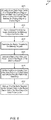
- FIG. 5 one embodiment of a method 500 for implementing an early probe mechanism is shown.
- the steps in this embodiment and those of FIG. 6 are shown in sequential order. However, it is noted that in various embodiments of the described methods, one or more of the elements described are performed concurrently, in a different order than shown, or are omitted entirely. Other additional elements are also performed as desired. Any of the various systems or apparatuses described herein are configured to implement method 500.
- a coherent slave unit performs parallel lookups to a probe filter and an early probe cache responsive to receiving a memory request (block 505). Prior to the lookup to the probe filter completing, the coherent slave unit sends an early probe to a first processing node responsive to determining a lookup to the early probe cache matches an entry identifying the first processing node as an owner of a first region targeted by the memory request (block 510). It is assumed for the purposes of this discussion that the confidence indicator of the matching entry in the early probe cache is greater than a programmable threshold.
- a demand probe can optionally be sent to the first processing node, depending on the embodiment (block 525).
- a lookup to the probe filter identifies a different processing node as an owner of the cache line targeted by the memory request (conditional block 515, "no" leg)
- the confidence indicator in the matching entry in the early probe cache is decremented and the LRU field is updated (block 530).
- the region owner field in the matching entry in the early probe cache is optionally updated with the correct processing node (block 535).
- a demand probe is sent to the correct processing node (block 540). After blocks 525 and 540, method 500 ends.
- FIG. 6 one embodiment of a method 600 for allocating region-based entries in an early probe cache for use in generating early probes is shown.
- a lookup to an early probe cache for a received memory request does not match any existing entries while a lookup to a probe filter matches an existing entry for a shared region (block 605). It is noted that the early probe cache lookup and probe filter lookup are performed in parallel by a coherent slave unit.
- a demand probe is sent to the target identified by the matching entry in the probe filter (block 610). Also, the region targeted by the memory request is determined (block 615).
- a new entry is allocated in the early probe cache for the region of the memory request (block 620). Any suitable eviction algorithm can be utilized to determine which entry to evict to make space for the new entry.
- the confidence indicator field of the new entry is set to a default value and the LRU field of the new entry is initialized (block 625).
- An ID of the node targeted by the demand probe is stored in the region owner field of the new entry in the early probe cache (block 630). Accordingly, for future memory requests targeting this region, an early probe will be sent to the same node based on this new entry in the early probe cache. After block 630, method 600 ends.
- program instructions of a software application are used to implement the methods and/or mechanisms described herein.
- program instructions executable by a general or special purpose processor are contemplated.
- such program instructions can be represented by a high level programming language.
- the program instructions can be compiled from a high level programming language to a binary, intermediate, or other form.
- program instructions can be written that describe the behavior or design of hardware.
- Such program instructions can be represented by a high-level programming language, such as C.
- a hardware design language (HDL) such as Verilog can be used.
- the program instructions are stored on any of a variety of non-transitory computer readable storage mediums. The storage medium is accessible by a computing system during use to provide the program instructions to the computing system for program execution.
- a computing system includes at least one or more memories and one or more processors configured to execute program instructions.
Landscapes
- Engineering & Computer Science (AREA)
- Theoretical Computer Science (AREA)
- Physics & Mathematics (AREA)
- General Engineering & Computer Science (AREA)
- General Physics & Mathematics (AREA)
- Memory System Of A Hierarchy Structure (AREA)
Priority Applications (1)
| Application Number | Priority Date | Filing Date | Title |
|---|---|---|---|
| EP21202235.4A EP3961409B1 (en) | 2017-12-15 | 2018-09-19 | Home agent based cache transfer acceleration scheme |
Applications Claiming Priority (2)
| Application Number | Priority Date | Filing Date | Title |
|---|---|---|---|
| US15/844,215 US10776282B2 (en) | 2017-12-15 | 2017-12-15 | Home agent based cache transfer acceleration scheme |
| PCT/US2018/051756 WO2019118037A1 (en) | 2017-12-15 | 2018-09-19 | Home agent based cache transfer acceleration scheme |
Related Child Applications (1)
| Application Number | Title | Priority Date | Filing Date |
|---|---|---|---|
| EP21202235.4A Division EP3961409B1 (en) | 2017-12-15 | 2018-09-19 | Home agent based cache transfer acceleration scheme |
Publications (2)
| Publication Number | Publication Date |
|---|---|
| EP3724772A1 EP3724772A1 (en) | 2020-10-21 |
| EP3724772B1 true EP3724772B1 (en) | 2021-10-27 |
Family
ID=63794694
Family Applications (2)
| Application Number | Title | Priority Date | Filing Date |
|---|---|---|---|
| EP18783262.1A Active EP3724772B1 (en) | 2017-12-15 | 2018-09-19 | Home agent based cache transfer acceleration scheme |
| EP21202235.4A Active EP3961409B1 (en) | 2017-12-15 | 2018-09-19 | Home agent based cache transfer acceleration scheme |
Family Applications After (1)
| Application Number | Title | Priority Date | Filing Date |
|---|---|---|---|
| EP21202235.4A Active EP3961409B1 (en) | 2017-12-15 | 2018-09-19 | Home agent based cache transfer acceleration scheme |
Country Status (6)
| Country | Link |
|---|---|
| US (2) | US10776282B2 (enExample) |
| EP (2) | EP3724772B1 (enExample) |
| JP (1) | JP6975335B2 (enExample) |
| KR (1) | KR102383040B1 (enExample) |
| CN (1) | CN111656332B (enExample) |
| WO (1) | WO2019118037A1 (enExample) |
Families Citing this family (5)
| Publication number | Priority date | Publication date | Assignee | Title |
|---|---|---|---|---|
| US10776282B2 (en) | 2017-12-15 | 2020-09-15 | Advanced Micro Devices, Inc. | Home agent based cache transfer acceleration scheme |
| US11210248B2 (en) * | 2019-12-20 | 2021-12-28 | Advanced Micro Devices, Inc. | System direct memory access engine offload |
| US11874783B2 (en) * | 2021-12-21 | 2024-01-16 | Advanced Micro Devices, Inc. | Coherent block read fulfillment |
| US20250240156A1 (en) * | 2022-12-23 | 2025-07-24 | Advanced Micro Devices, Inc. | Systems and methods relating to confidential computing key mixing hazard management |
| CN117651021B (zh) * | 2024-01-25 | 2024-04-30 | 苏州萨沙迈半导体有限公司 | 过滤器及其控制方法和装置、电气设备 |
Family Cites Families (17)
| Publication number | Priority date | Publication date | Assignee | Title |
|---|---|---|---|---|
| US6055610A (en) * | 1997-08-25 | 2000-04-25 | Hewlett-Packard Company | Distributed memory multiprocessor computer system with directory based cache coherency with ambiguous mapping of cached data to main-memory locations |
| US6631401B1 (en) | 1998-12-21 | 2003-10-07 | Advanced Micro Devices, Inc. | Flexible probe/probe response routing for maintaining coherency |
| US7234029B2 (en) * | 2000-12-28 | 2007-06-19 | Intel Corporation | Method and apparatus for reducing memory latency in a cache coherent multi-node architecture |
| US7395375B2 (en) * | 2004-11-08 | 2008-07-01 | International Business Machines Corporation | Prefetch miss indicator for cache coherence directory misses on external caches |
| JP5103396B2 (ja) | 2005-08-23 | 2012-12-19 | アドバンスト・マイクロ・ディバイシズ・インコーポレイテッド | コンピュータシステムにおいて能動的に同期をとる方法 |
| US8185695B2 (en) * | 2008-06-30 | 2012-05-22 | Advanced Micro Devices, Inc. | Snoop filtering mechanism |
| JP5136652B2 (ja) * | 2008-11-10 | 2013-02-06 | 富士通株式会社 | 情報処理装置及びメモリ制御装置 |
| US9081706B2 (en) * | 2012-05-10 | 2015-07-14 | Oracle International Corporation | Using a shared last-level TLB to reduce address-translation latency |
| US9405687B2 (en) * | 2013-11-04 | 2016-08-02 | Intel Corporation | Method, apparatus and system for handling cache misses in a processor |
| US9639470B2 (en) * | 2014-08-26 | 2017-05-02 | Arm Limited | Coherency checking of invalidate transactions caused by snoop filter eviction in an integrated circuit |
| DE102015115582A1 (de) | 2014-10-22 | 2016-04-28 | Imagination Technologies Limited | Vorrichtung und Verfahren zum Drosseln des Hardwarevorauslesens |
| CN104331377B (zh) | 2014-11-12 | 2018-06-26 | 浪潮(北京)电子信息产业有限公司 | 一种多核处理器系统的目录缓存管理方法 |
| US11237965B2 (en) * | 2014-12-31 | 2022-02-01 | Arteris, Inc. | Configurable snoop filters for cache coherent systems |
| US9792210B2 (en) | 2015-12-22 | 2017-10-17 | Advanced Micro Devices, Inc. | Region probe filter for distributed memory system |
| US9817760B2 (en) * | 2016-03-07 | 2017-11-14 | Qualcomm Incorporated | Self-healing coarse-grained snoop filter |
| US11061572B2 (en) * | 2016-04-22 | 2021-07-13 | Advanced Micro Devices, Inc. | Memory object tagged memory monitoring method and system |
| US10776282B2 (en) | 2017-12-15 | 2020-09-15 | Advanced Micro Devices, Inc. | Home agent based cache transfer acceleration scheme |
-
2017
- 2017-12-15 US US15/844,215 patent/US10776282B2/en active Active
-
2018
- 2018-09-19 CN CN201880088010.1A patent/CN111656332B/zh active Active
- 2018-09-19 KR KR1020207020385A patent/KR102383040B1/ko active Active
- 2018-09-19 EP EP18783262.1A patent/EP3724772B1/en active Active
- 2018-09-19 EP EP21202235.4A patent/EP3961409B1/en active Active
- 2018-09-19 JP JP2020532672A patent/JP6975335B2/ja active Active
- 2018-09-19 WO PCT/US2018/051756 patent/WO2019118037A1/en not_active Ceased
-
2020
- 2020-09-14 US US17/019,999 patent/US11782848B2/en active Active
Also Published As
| Publication number | Publication date |
|---|---|
| KR102383040B1 (ko) | 2022-04-08 |
| US10776282B2 (en) | 2020-09-15 |
| US20190188155A1 (en) | 2019-06-20 |
| JP2021507371A (ja) | 2021-02-22 |
| CN111656332A (zh) | 2020-09-11 |
| CN111656332B (zh) | 2024-08-27 |
| JP6975335B2 (ja) | 2021-12-01 |
| WO2019118037A1 (en) | 2019-06-20 |
| US20210064545A1 (en) | 2021-03-04 |
| EP3724772A1 (en) | 2020-10-21 |
| US11782848B2 (en) | 2023-10-10 |
| KR20200096975A (ko) | 2020-08-14 |
| EP3961409A1 (en) | 2022-03-02 |
| EP3961409B1 (en) | 2024-04-10 |
Similar Documents
| Publication | Publication Date | Title |
|---|---|---|
| JP7390304B2 (ja) | 大規模なキャッシュサイズに適合する領域ベースのディレクトリスキーム | |
| US11782848B2 (en) | Home agent based cache transfer acceleration scheme | |
| EP4035015B1 (en) | System probe aware last level cache insertion bypassing | |
| JP7036988B2 (ja) | 領域ベースのキャッシュディレクトリスキームにおけるプライベート領域へのアクセスの加速 | |
| US12332795B2 (en) | Reducing probe filter accesses for processing in memory requests | |
| US10503648B2 (en) | Cache to cache data transfer acceleration techniques | |
| US10545875B2 (en) | Tag accelerator for low latency DRAM cache |
Legal Events
| Date | Code | Title | Description |
|---|---|---|---|
| STAA | Information on the status of an ep patent application or granted ep patent |
Free format text: STATUS: UNKNOWN |
|
| STAA | Information on the status of an ep patent application or granted ep patent |
Free format text: STATUS: THE INTERNATIONAL PUBLICATION HAS BEEN MADE |
|
| PUAI | Public reference made under article 153(3) epc to a published international application that has entered the european phase |
Free format text: ORIGINAL CODE: 0009012 |
|
| STAA | Information on the status of an ep patent application or granted ep patent |
Free format text: STATUS: REQUEST FOR EXAMINATION WAS MADE |
|
| 17P | Request for examination filed |
Effective date: 20200713 |
|
| AK | Designated contracting states |
Kind code of ref document: A1 Designated state(s): AL AT BE BG CH CY CZ DE DK EE ES FI FR GB GR HR HU IE IS IT LI LT LU LV MC MK MT NL NO PL PT RO RS SE SI SK SM TR |
|
| AX | Request for extension of the european patent |
Extension state: BA ME |
|
| RIN1 | Information on inventor provided before grant (corrected) |
Inventor name: LEPAK, KEVIN M. Inventor name: BALAKRISHNAN, GANESH Inventor name: APTE, AMIT P. Inventor name: KALYANASUNDHARAM, VYDHYANATHAN |
|
| DAV | Request for validation of the european patent (deleted) | ||
| DAX | Request for extension of the european patent (deleted) | ||
| GRAP | Despatch of communication of intention to grant a patent |
Free format text: ORIGINAL CODE: EPIDOSNIGR1 |
|
| STAA | Information on the status of an ep patent application or granted ep patent |
Free format text: STATUS: GRANT OF PATENT IS INTENDED |
|
| INTG | Intention to grant announced |
Effective date: 20210519 |
|
| GRAS | Grant fee paid |
Free format text: ORIGINAL CODE: EPIDOSNIGR3 |
|
| GRAA | (expected) grant |
Free format text: ORIGINAL CODE: 0009210 |
|
| STAA | Information on the status of an ep patent application or granted ep patent |
Free format text: STATUS: THE PATENT HAS BEEN GRANTED |
|
| AK | Designated contracting states |
Kind code of ref document: B1 Designated state(s): AL AT BE BG CH CY CZ DE DK EE ES FI FR GB GR HR HU IE IS IT LI LT LU LV MC MK MT NL NO PL PT RO RS SE SI SK SM TR |
|
| REG | Reference to a national code |
Ref country code: GB Ref legal event code: FG4D |
|
| REG | Reference to a national code |
Ref country code: CH Ref legal event code: EP |
|
| REG | Reference to a national code |
Ref country code: AT Ref legal event code: REF Ref document number: 1442422 Country of ref document: AT Kind code of ref document: T Effective date: 20211115 |
|
| REG | Reference to a national code |
Ref country code: DE Ref legal event code: R096 Ref document number: 602018025793 Country of ref document: DE |
|
| REG | Reference to a national code |
Ref country code: IE Ref legal event code: FG4D |
|
| REG | Reference to a national code |
Ref country code: LT Ref legal event code: MG9D |
|
| REG | Reference to a national code |
Ref country code: NL Ref legal event code: MP Effective date: 20211027 |
|
| REG | Reference to a national code |
Ref country code: AT Ref legal event code: MK05 Ref document number: 1442422 Country of ref document: AT Kind code of ref document: T Effective date: 20211027 |
|
| PG25 | Lapsed in a contracting state [announced via postgrant information from national office to epo] |
Ref country code: RS Free format text: LAPSE BECAUSE OF FAILURE TO SUBMIT A TRANSLATION OF THE DESCRIPTION OR TO PAY THE FEE WITHIN THE PRESCRIBED TIME-LIMIT Effective date: 20211027 Ref country code: LT Free format text: LAPSE BECAUSE OF FAILURE TO SUBMIT A TRANSLATION OF THE DESCRIPTION OR TO PAY THE FEE WITHIN THE PRESCRIBED TIME-LIMIT Effective date: 20211027 Ref country code: FI Free format text: LAPSE BECAUSE OF FAILURE TO SUBMIT A TRANSLATION OF THE DESCRIPTION OR TO PAY THE FEE WITHIN THE PRESCRIBED TIME-LIMIT Effective date: 20211027 Ref country code: BG Free format text: LAPSE BECAUSE OF FAILURE TO SUBMIT A TRANSLATION OF THE DESCRIPTION OR TO PAY THE FEE WITHIN THE PRESCRIBED TIME-LIMIT Effective date: 20220127 Ref country code: AT Free format text: LAPSE BECAUSE OF FAILURE TO SUBMIT A TRANSLATION OF THE DESCRIPTION OR TO PAY THE FEE WITHIN THE PRESCRIBED TIME-LIMIT Effective date: 20211027 |
|
| PG25 | Lapsed in a contracting state [announced via postgrant information from national office to epo] |
Ref country code: IS Free format text: LAPSE BECAUSE OF FAILURE TO SUBMIT A TRANSLATION OF THE DESCRIPTION OR TO PAY THE FEE WITHIN THE PRESCRIBED TIME-LIMIT Effective date: 20220227 Ref country code: SE Free format text: LAPSE BECAUSE OF FAILURE TO SUBMIT A TRANSLATION OF THE DESCRIPTION OR TO PAY THE FEE WITHIN THE PRESCRIBED TIME-LIMIT Effective date: 20211027 Ref country code: PT Free format text: LAPSE BECAUSE OF FAILURE TO SUBMIT A TRANSLATION OF THE DESCRIPTION OR TO PAY THE FEE WITHIN THE PRESCRIBED TIME-LIMIT Effective date: 20220228 Ref country code: PL Free format text: LAPSE BECAUSE OF FAILURE TO SUBMIT A TRANSLATION OF THE DESCRIPTION OR TO PAY THE FEE WITHIN THE PRESCRIBED TIME-LIMIT Effective date: 20211027 Ref country code: NO Free format text: LAPSE BECAUSE OF FAILURE TO SUBMIT A TRANSLATION OF THE DESCRIPTION OR TO PAY THE FEE WITHIN THE PRESCRIBED TIME-LIMIT Effective date: 20220127 Ref country code: NL Free format text: LAPSE BECAUSE OF FAILURE TO SUBMIT A TRANSLATION OF THE DESCRIPTION OR TO PAY THE FEE WITHIN THE PRESCRIBED TIME-LIMIT Effective date: 20211027 Ref country code: LV Free format text: LAPSE BECAUSE OF FAILURE TO SUBMIT A TRANSLATION OF THE DESCRIPTION OR TO PAY THE FEE WITHIN THE PRESCRIBED TIME-LIMIT Effective date: 20211027 Ref country code: HR Free format text: LAPSE BECAUSE OF FAILURE TO SUBMIT A TRANSLATION OF THE DESCRIPTION OR TO PAY THE FEE WITHIN THE PRESCRIBED TIME-LIMIT Effective date: 20211027 Ref country code: GR Free format text: LAPSE BECAUSE OF FAILURE TO SUBMIT A TRANSLATION OF THE DESCRIPTION OR TO PAY THE FEE WITHIN THE PRESCRIBED TIME-LIMIT Effective date: 20220128 Ref country code: ES Free format text: LAPSE BECAUSE OF FAILURE TO SUBMIT A TRANSLATION OF THE DESCRIPTION OR TO PAY THE FEE WITHIN THE PRESCRIBED TIME-LIMIT Effective date: 20211027 |
|
| REG | Reference to a national code |
Ref country code: DE Ref legal event code: R097 Ref document number: 602018025793 Country of ref document: DE |
|
| PG25 | Lapsed in a contracting state [announced via postgrant information from national office to epo] |
Ref country code: SM Free format text: LAPSE BECAUSE OF FAILURE TO SUBMIT A TRANSLATION OF THE DESCRIPTION OR TO PAY THE FEE WITHIN THE PRESCRIBED TIME-LIMIT Effective date: 20211027 Ref country code: SK Free format text: LAPSE BECAUSE OF FAILURE TO SUBMIT A TRANSLATION OF THE DESCRIPTION OR TO PAY THE FEE WITHIN THE PRESCRIBED TIME-LIMIT Effective date: 20211027 Ref country code: RO Free format text: LAPSE BECAUSE OF FAILURE TO SUBMIT A TRANSLATION OF THE DESCRIPTION OR TO PAY THE FEE WITHIN THE PRESCRIBED TIME-LIMIT Effective date: 20211027 Ref country code: EE Free format text: LAPSE BECAUSE OF FAILURE TO SUBMIT A TRANSLATION OF THE DESCRIPTION OR TO PAY THE FEE WITHIN THE PRESCRIBED TIME-LIMIT Effective date: 20211027 Ref country code: DK Free format text: LAPSE BECAUSE OF FAILURE TO SUBMIT A TRANSLATION OF THE DESCRIPTION OR TO PAY THE FEE WITHIN THE PRESCRIBED TIME-LIMIT Effective date: 20211027 Ref country code: CZ Free format text: LAPSE BECAUSE OF FAILURE TO SUBMIT A TRANSLATION OF THE DESCRIPTION OR TO PAY THE FEE WITHIN THE PRESCRIBED TIME-LIMIT Effective date: 20211027 |
|
| PLBE | No opposition filed within time limit |
Free format text: ORIGINAL CODE: 0009261 |
|
| STAA | Information on the status of an ep patent application or granted ep patent |
Free format text: STATUS: NO OPPOSITION FILED WITHIN TIME LIMIT |
|
| 26N | No opposition filed |
Effective date: 20220728 |
|
| PG25 | Lapsed in a contracting state [announced via postgrant information from national office to epo] |
Ref country code: AL Free format text: LAPSE BECAUSE OF FAILURE TO SUBMIT A TRANSLATION OF THE DESCRIPTION OR TO PAY THE FEE WITHIN THE PRESCRIBED TIME-LIMIT Effective date: 20211027 |
|
| PG25 | Lapsed in a contracting state [announced via postgrant information from national office to epo] |
Ref country code: SI Free format text: LAPSE BECAUSE OF FAILURE TO SUBMIT A TRANSLATION OF THE DESCRIPTION OR TO PAY THE FEE WITHIN THE PRESCRIBED TIME-LIMIT Effective date: 20211027 |
|
| PG25 | Lapsed in a contracting state [announced via postgrant information from national office to epo] |
Ref country code: MC Free format text: LAPSE BECAUSE OF FAILURE TO SUBMIT A TRANSLATION OF THE DESCRIPTION OR TO PAY THE FEE WITHIN THE PRESCRIBED TIME-LIMIT Effective date: 20211027 |
|
| REG | Reference to a national code |
Ref country code: CH Ref legal event code: PL |
|
| REG | Reference to a national code |
Ref country code: BE Ref legal event code: MM Effective date: 20220930 |
|
| PG25 | Lapsed in a contracting state [announced via postgrant information from national office to epo] |
Ref country code: IT Free format text: LAPSE BECAUSE OF FAILURE TO SUBMIT A TRANSLATION OF THE DESCRIPTION OR TO PAY THE FEE WITHIN THE PRESCRIBED TIME-LIMIT Effective date: 20211027 |
|
| PG25 | Lapsed in a contracting state [announced via postgrant information from national office to epo] |
Ref country code: LU Free format text: LAPSE BECAUSE OF NON-PAYMENT OF DUE FEES Effective date: 20220919 |
|
| P01 | Opt-out of the competence of the unified patent court (upc) registered |
Effective date: 20230530 |
|
| PG25 | Lapsed in a contracting state [announced via postgrant information from national office to epo] |
Ref country code: LI Free format text: LAPSE BECAUSE OF NON-PAYMENT OF DUE FEES Effective date: 20220930 Ref country code: IE Free format text: LAPSE BECAUSE OF NON-PAYMENT OF DUE FEES Effective date: 20220919 Ref country code: FR Free format text: LAPSE BECAUSE OF NON-PAYMENT OF DUE FEES Effective date: 20220930 Ref country code: CH Free format text: LAPSE BECAUSE OF NON-PAYMENT OF DUE FEES Effective date: 20220930 |
|
| PG25 | Lapsed in a contracting state [announced via postgrant information from national office to epo] |
Ref country code: BE Free format text: LAPSE BECAUSE OF NON-PAYMENT OF DUE FEES Effective date: 20220930 |
|
| PG25 | Lapsed in a contracting state [announced via postgrant information from national office to epo] |
Ref country code: CY Free format text: LAPSE BECAUSE OF FAILURE TO SUBMIT A TRANSLATION OF THE DESCRIPTION OR TO PAY THE FEE WITHIN THE PRESCRIBED TIME-LIMIT Effective date: 20211027 |
|
| PG25 | Lapsed in a contracting state [announced via postgrant information from national office to epo] |
Ref country code: MK Free format text: LAPSE BECAUSE OF FAILURE TO SUBMIT A TRANSLATION OF THE DESCRIPTION OR TO PAY THE FEE WITHIN THE PRESCRIBED TIME-LIMIT Effective date: 20211027 Ref country code: HU Free format text: LAPSE BECAUSE OF FAILURE TO SUBMIT A TRANSLATION OF THE DESCRIPTION OR TO PAY THE FEE WITHIN THE PRESCRIBED TIME-LIMIT; INVALID AB INITIO Effective date: 20180919 |
|
| PG25 | Lapsed in a contracting state [announced via postgrant information from national office to epo] |
Ref country code: TR Free format text: LAPSE BECAUSE OF FAILURE TO SUBMIT A TRANSLATION OF THE DESCRIPTION OR TO PAY THE FEE WITHIN THE PRESCRIBED TIME-LIMIT Effective date: 20211027 |
|
| PG25 | Lapsed in a contracting state [announced via postgrant information from national office to epo] |
Ref country code: MT Free format text: LAPSE BECAUSE OF FAILURE TO SUBMIT A TRANSLATION OF THE DESCRIPTION OR TO PAY THE FEE WITHIN THE PRESCRIBED TIME-LIMIT Effective date: 20211027 |
|
| PGFP | Annual fee paid to national office [announced via postgrant information from national office to epo] |
Ref country code: DE Payment date: 20250819 Year of fee payment: 8 |
|
| PGFP | Annual fee paid to national office [announced via postgrant information from national office to epo] |
Ref country code: GB Payment date: 20250911 Year of fee payment: 8 |