EP3724741B1 - Asynchronous buffer with pointer offsets - Google Patents
Asynchronous buffer with pointer offsets Download PDFInfo
- Publication number
- EP3724741B1 EP3724741B1 EP18888385.4A EP18888385A EP3724741B1 EP 3724741 B1 EP3724741 B1 EP 3724741B1 EP 18888385 A EP18888385 A EP 18888385A EP 3724741 B1 EP3724741 B1 EP 3724741B1
- Authority
- EP
- European Patent Office
- Prior art keywords
- write
- read
- clock
- pointer
- fifo
- Prior art date
- Legal status (The legal status is an assumption and is not a legal conclusion. Google has not performed a legal analysis and makes no representation as to the accuracy of the status listed.)
- Active
Links
Images


Classifications
-
- G—PHYSICS
- G06—COMPUTING OR CALCULATING; COUNTING
- G06F—ELECTRIC DIGITAL DATA PROCESSING
- G06F1/00—Details not covered by groups G06F3/00 - G06F13/00 and G06F21/00
- G06F1/04—Generating or distributing clock signals or signals derived directly therefrom
- G06F1/08—Clock generators with changeable or programmable clock frequency
-
- G—PHYSICS
- G06—COMPUTING OR CALCULATING; COUNTING
- G06F—ELECTRIC DIGITAL DATA PROCESSING
- G06F13/00—Interconnection of, or transfer of information or other signals between, memories, input/output devices or central processing units
- G06F13/14—Handling requests for interconnection or transfer
- G06F13/16—Handling requests for interconnection or transfer for access to memory bus
- G06F13/1605—Handling requests for interconnection or transfer for access to memory bus based on arbitration
- G06F13/161—Handling requests for interconnection or transfer for access to memory bus based on arbitration with latency improvement
-
- G—PHYSICS
- G06—COMPUTING OR CALCULATING; COUNTING
- G06F—ELECTRIC DIGITAL DATA PROCESSING
- G06F13/00—Interconnection of, or transfer of information or other signals between, memories, input/output devices or central processing units
- G06F13/14—Handling requests for interconnection or transfer
- G06F13/16—Handling requests for interconnection or transfer for access to memory bus
- G06F13/1668—Details of memory controller
- G06F13/1673—Details of memory controller using buffers
-
- G—PHYSICS
- G06—COMPUTING OR CALCULATING; COUNTING
- G06F—ELECTRIC DIGITAL DATA PROCESSING
- G06F13/00—Interconnection of, or transfer of information or other signals between, memories, input/output devices or central processing units
- G06F13/38—Information transfer, e.g. on bus
- G06F13/40—Bus structure
- G06F13/4004—Coupling between buses
- G06F13/4027—Coupling between buses using bus bridges
- G06F13/405—Coupling between buses using bus bridges where the bridge performs a synchronising function
- G06F13/4059—Coupling between buses using bus bridges where the bridge performs a synchronising function where the synchronisation uses buffers, e.g. for speed matching between buses
-
- G—PHYSICS
- G06—COMPUTING OR CALCULATING; COUNTING
- G06F—ELECTRIC DIGITAL DATA PROCESSING
- G06F13/00—Interconnection of, or transfer of information or other signals between, memories, input/output devices or central processing units
- G06F13/38—Information transfer, e.g. on bus
- G06F13/42—Bus transfer protocol, e.g. handshake; Synchronisation
- G06F13/4204—Bus transfer protocol, e.g. handshake; Synchronisation on a parallel bus
- G06F13/4234—Bus transfer protocol, e.g. handshake; Synchronisation on a parallel bus being a memory bus
- G06F13/4239—Bus transfer protocol, e.g. handshake; Synchronisation on a parallel bus being a memory bus with asynchronous protocol
-
- G—PHYSICS
- G06—COMPUTING OR CALCULATING; COUNTING
- G06F—ELECTRIC DIGITAL DATA PROCESSING
- G06F5/00—Methods or arrangements for data conversion without changing the order or content of the data handled
- G06F5/06—Methods or arrangements for data conversion without changing the order or content of the data handled for changing the speed of data flow, i.e. speed regularising or timing, e.g. delay lines, FIFO buffers; over- or underrun control therefor
- G06F5/10—Methods or arrangements for data conversion without changing the order or content of the data handled for changing the speed of data flow, i.e. speed regularising or timing, e.g. delay lines, FIFO buffers; over- or underrun control therefor having a sequence of storage locations each being individually accessible for both enqueue and dequeue operations, e.g. using random access memory
- G06F5/12—Means for monitoring the fill level; Means for resolving contention, i.e. conflicts between simultaneous enqueue and dequeue operations
- G06F5/14—Means for monitoring the fill level; Means for resolving contention, i.e. conflicts between simultaneous enqueue and dequeue operations for overflow or underflow handling, e.g. full or empty flags
-
- G—PHYSICS
- G06—COMPUTING OR CALCULATING; COUNTING
- G06F—ELECTRIC DIGITAL DATA PROCESSING
- G06F2205/00—Indexing scheme relating to group G06F5/00; Methods or arrangements for data conversion without changing the order or content of the data handled
- G06F2205/12—Indexing scheme relating to groups G06F5/12 - G06F5/14
- G06F2205/126—Monitoring of intermediate fill level, i.e. with additional means for monitoring the fill level, e.g. half full flag, almost empty flag
Definitions
- a processor typically employs one or more clock signals to synchronize logic operations at modules of the processor, thereby preventing errors such as setup errors, race conditions, and the like.
- a typical processor employs different clock signals for different portions of the processor, wherein each processor portion is referred to as a clock domain.
- the clock signals for the different clock domains are relatively independent of each other, allowing the logic operations of different clock domains to be synchronized independently of other clock domains.
- the processor can synchronize the different clock domains with clock signals of different frequencies, thereby improving processing efficiency.
- the independence of the clock signals supports simplified clock management and signal routing at the processor. However, in many instances data must be communicated between modules of different clock domains, whereby such communication can cause meta-stability errors in the data.
- the present invention provides a method in accordance with claim 1 and a processor in accordance with claim 7.
- FIGs. 1-7 illustrate techniques for applying offset values to read and write pointers to a FIFO for data being transferred between clock domains of a processor based on a frequency ratio between the clock domains, allowing data to be written to or read from the FIFO at a faster rate than that governed by meta-stability circuitry associated with the read and write pointers.
- the processor employs one or more controllers that set and apply pointer offsets in each of the clock domains to reduce latency while ensuring that data is not read by the receiving clock domain from an entry of the FIFO until after the data has been written to the entry, thereby reducing data transfer errors. Further, the controller resets the pointer offset values in response to a change in clock frequency at one or both of the clock domains.
- the processor continues to accurately transfer data in response to clock frequency changes, while reducing latency and maximizing bandwidth.
- the processor enhances processing efficiency while supporting accurate data transfer between the clock domains.
- the processor includes a first-in first out queue (FIFO) having multiple entries to store data transferred between two different clock domains.
- Each clock domain includes a controller to manage a set of pointers to access the FIFO.
- the read and write pointers are transferred across the clock domains via a meta-stability circuit to ensure that data is not written to or read from a FIFO entry until a read or write of the entry has been completed.
- the timing and configuration of the meta-stability circuit is based on an assumed "worst-case" relationship between the clock signals of the different clock domains.
- the assumed worst-case relationship is too conservative in many cases, negatively impacting processing efficiency.
- the FIFO controller applies a non-zero offset value to one or more of the read and write pointers based on the frequencies of the clock signals of the different clock domains, thereby allowing the FIFO to be read or written more quickly.
- the controller thereby ensures that a lower latency is established for data written to the FIFO before that data is read. For example, for some embodiments in which the frequencies of the clock domains are equal, the controller sets a positive write pointer offset value and a positive read pointer offset value that reduce the latency of the FIFO by several clock cycles.
- the frequency of the write clock is higher than the frequency of the read clock
- the controller sets a negative offset value for the write pointer to reduce the time entries sit in the FIFO and a positive offset value for the read pointer to prevent the read side from stalling as it waits for the pointers to synchronize, resulting in reduced latency and increased bandwidth.
- Both clock domains of the FIFO move their read and write pointers at constant rates, even if there is no data to transfer, based on the known frequency (or period) ratio. The constancy of the transfer rate allows the application of appropriate offsets that would otherwise be unsafe if the frequencies were unknown or fluctuating beyond margined limits.
- FIG. 1 illustrates a processor 100 that applies offset values to read and write pointers to a FIFO for data being transferred between clock domains of a processor based on a frequency ratio between the clock domains, and resets the offset values in response to a frequency change in a clock signal for at least one of the clock domains in accordance with some embodiments.
- the processor 100 is implemented by any of a variety of compute-enabled electronic devices, such as a server, a desktop computer, a notebook computer, a tablet computer, a compute-enabled portable cellular phone (e.g., a "smart phone"), a compute-enabled watch or other wearable item, a personal digital assistant (PDA), a gaming console, and the like.
- PDA personal digital assistant
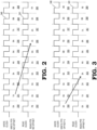
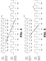
- the controller 106 shortens the latency of the FIFO 110 from 5 cycles, as depicted in FIG. 2, to 3 cycles, as depicted in FIG. 3 .
- FIG. 4 illustrates an example of the controller 106 of FIG. 1 applying a write offset 150 of zero to the write pointer 115 and a read offset 155 of zero to the read pointer 125 for writes to and reads from the FIFO 110 in accordance with some embodiments.
- FIG. 4 illustrates waveforms 440 and 441, corresponding to examples of the WRITE CLOCK and READ CLOCK signals, respectively.
- the READ CLOCK signal is 50% slower than the WRITE CLOCK signal.
- the waveforms 440 and 441 are each divided into cycles: cycles 450-459 of the WRITE CLOCK (waveform 440) and cycles 460-469 of the READ CLOCK (waveform 441).
- the FIFO 110 has a depth of 8 entries
- the read pointer sync 130 and write pointer sync 135 each have a depth of 4 flip flops
- the heads up signal 160 specifies a 1 cycle delay
- the ready signal 165 specifies a 2 cycle delay.
- the most significant bits (MSB) of the write pointer 115 and the read pointer 125 are illustrated in FIG. 4 as having a value of either A or B.
- FIG. 5 illustrates an example of the controller 106 of FIG. 1 applying a write offset 150 of -1 to the write pointer 115 and a read offset 155 of 2 to the read pointer 125 for writes to and reads from the FIFO 110 in accordance with some embodiments. Similar to FIG. 4, FIG. 5 illustrates waveforms 540 and 541, corresponding to examples of the WRITE CLOCK and READ CLOCK signals, respectively.
- the waveforms 540 and 541 are each divided into cycles: cycles 550-559 of the WRITE CLOCK (waveform 540) and cycles 560-569 of the READ CLOCK (waveform 541).
- FIG. 5 illustrates the location of the FIFO 110 that is indicated by the write pointer 115 for data to be written by the write module 140
- FIG. 5 illustrates the location of the FIFO 110 that is indicated by the read pointer 125 for data to be read by the read module 145.
- the FIFO 110 has a depth of 8 entries
- the read pointer sync 130 and write pointer sync 135 each have a depth of 4 flip flops
- the heads up signal 160 specifies a 1 cycle delay
- the ready signal 165 specifies a 2 cycle delay.
- the most significant bits (MSB) of the write pointer 115 and the read pointer 125 are illustrated in FIG. 5 as having a value of either A or B.
- the write module 140 writes to location 2 of the FIFO 110 during cycle 550, to location 3 of the FIFO 110 during cycle 551, to location 4 of the FIFO during cycle 553, to location 5 during cycle 554, and so on through cycle 557, when the write module 140 writes to location 7 of the FIFO 110, after which the write module 140 writes to location 0 in cycle 559.
- the read module 145 reads the data from location 5 of the FIFO 110 during cycle 565 of the READ CLOCK, which is 4 cycles of the WRITE CLOCK and 3 cycles of the READ CLOCK after the data was written to location 5 of the FIFO 110.
- the controller 106 shortens the latency of the FIFO 110 from 7 cycles of the WRITE CLOCK and 5 cycles of the READ CLOCK, as depicted in FIG. 4, to 4 cycles of the WRITE CLOCK and 3 cycles of the READ CLOCK, as depicted in FIG. 5 .
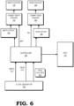
- FIG. 6 illustrates a block diagram of the controller 106 of FIG. 1 in accordance with some embodiments.
- the controller 106 calculates and applies the write offset 150 and the read offset 155 to the commit write pointer 170 and commit read pointer 180, respectively.
- the commit write pointer 170 and the commit read pointer 180 directly control the write pointer 115 and the read pointer 125, respectively, through a pipeline of flip flops.
- the depth of the pipeline of flip flops depends on the delays of the read and heads up signals (not shown). For example, if the ready depth is zero and the heads up depth is zero, then the commit write pointer 170 and the commit read pointer 180 are effectively removed.
- the controller 106 is able to anticipate the number of transfers into or out of each side of the FIFO 110 that will have taken place during the delay between the time at which a location of the FIFO 110 is written to by the write module 140 and the time that location of the FIFO 110 is read from by the read module 145.
- the controller 106 applies offset values for the write offset 150 and the read offset 155 that allow the commit write pointer 170 and the commit read pointer 180 to move beyond the raw values they would otherwise have indicated while maintaining a margin sufficient to ensure that the read module 145 reads to correct value from the location of the FIFO 110 indicated by the commit read pointer 180 and that the write module 140 does not overwrite a value at a location of the FIFO 110 that has not yet been read by the read module 145.
- the processor 100 includes the clock generator 108, the controller 106, the read offset 155, the commit read pointer 180, the read pointer module 125, the write offset 150, the commit write pointer 170, the write pointer module 115, and the FIFO 110.
- the read pointer module 125 is configured to store the read pointer for the read module (not shown).
- the commit read pointer 180 adjusts the read pointer module 125 to point to the next location of the FIFO 110, and the read pointer module 125 in turn provides the read pointer to the FIFO 110.
- the FIFO 110 reads the location indicated by the read pointer and provides the read data to the read module.
- the write pointer module 115 is configured similarly to the read pointer module 125 to write data to the FIFO 110.
- the write pointer module 115 stores the write pointer for the write module (not shown).
- the commit write pointer 170 adjusts the write pointer module 115 to point to the next location of the FIFO 110, and the write pointer module 115 in turn provides the write pointer to the FIFO 110, along with the data provided by the write module (not shown).
- the FIFO 110 writes the data location indicated by the write pointer.
- the controller 106 is configured to generate the RD and WRT signals to read and write data from and to the FIFO 110 to calculate and apply the write offset 150 and the read offset 155 as described above with respect to FIGs. 1 , 3 , and 5 .
- the controller 106 receives a frequency change request 610 from the clock generator 108.
- the frequency change request 610 indicates that the clock generator 108 will change the frequency of one or both of the WRITE CLK and the READ CLK.
- the controller 106 calculates the new write offset 150 and read offset 155 based on the adjusted frequencies of the WRITE CLK and READ CLK.
- the controller 106 then waits for the write pointer 115 and the read pointer 125 to pass a first common entry of the FIFO 110 and then temporarily halts transfers of data from components of the processor 100 and empties the entries of the FIFO 110 that include data that has not been accessed by the read module.
- the controller 106 stops the write pointer 115 and the read pointer 125 at a second common entry of the FIFO 110 and applies the new write offset 150 and the new read offset 155.
- the controller 106 then restarts the write pointer 115 and the read pointer 150 and re-enables transfers of data from components of the processor 100.
- FIG. 7 is a flow diagram of a method 700 of setting a write offset 150 and a read offset 155 for transferring data between clock domains at a FIFO in response to a frequency change of a clock signal for one or both of the clock domains in accordance with some embodiments.
- the method 700 is implemented in some embodiments of the processor 100 shown in FIG. 1 .
- Controller 106 performs method 700 whenever new a new write offset 150 or a new read offset 155 are needed before and after one or both of WRITE CLK and READ CLK change frequency.
- Method 700 ensures no data is lost or duplicated when the write offset 150 and read offset 155 change by stopping transfers through the FIFO 110, flushing all pending entries from the FIFO 110, stopping the write pointer 115 and read pointer 125 at a fixed location, applying the new write offset 150 and read offset 155 values, restarting the write pointer 115 and the read pointer 125 in a controlled fashion, and finally resuming data transfers though the FIFO 110.
- the controller 106 operates two parallel instances of method 700, one for the write clock domain 102 and another for the read clock domain 104. At several points in method 700 the write pointer 115 and the read pointer 125 are required to operate in a coordinated fashion such that parallel versions in read clock domain 102 and write clock domain 104 of method 700 are in the same block 702 through 724 at the same time or nearly the same time as required for proper operation.
- the controller 106 determines if a frequency change is in progress and if a new write offset 150 and a read offset 155 are required. If not, the method flow returns to block 702. If a new write offset 150 and a read offset 155 are required, at block 704, the controller 106 calculates the new write offset 150 and read offset 155. At block 706, the controller 106 waits for the read pointer 115 and write pointer 125 to pass a first common reference point.
- the common reference point is a defined position in the FIFO 110 that the instances of method 700 in the write clock domain 102 and the read clock domain 104 agree upon. In some embodiments, the common reference point is the FIFO 110 entry 0A.
- the common reference point is a FIFO 110 entry as tracked by the commit write pointer 170 and the commit read pointer 180.
- Use of the commit write pointer 170 and the commit read pointer 180 ensures that every pulse of ready signal 165 has a corresponding heads up signal 160 and that entries still in the FIFO 110 at the entry of block 708 will still be read by the read module 145 and have a corresponding pulse of heads up signal 160.
- controller 106 forces the ready signal 165 and heads up signal 160 values low to inform components connected to processor 100 that no transfers are available. However, while components outside processor 100 are stalled, write pointer 115 and read pointer 125 continue to operate within processor 100 to perform method 700. At block 710, controller 106 drains any data in the FIFO 110 that is waiting to be read by the read module 145.
- the forcing of ready signal 165 and heads up signal 160 low through the commit write pointer 170 and commit read pointer 180 ensures that any transfers through the FIFO 110 when method 700 reaches block 708 will still have a proper heads up signal 160 as the flip flop pipeline used inside the commit write pointer 170 and the commit read pointer 180 will contain the proper values to operate the write pointer 115 and read pointer 125, respectively, to prevent lost data.
- the controller 106 applies the new read write offset 150 and new read offset 155.
- the controller 106 restarts the write pointer 115 upon detecting that the read pointer sync 130 has reached the second common reference point.
- the read pointer 125 detects that the write pointer sync 136 moves past the second common reference point.
- the commit read pointer 180 bypasses the internal flip flop pipeline and begins moving the read pointer 125 and the commit read pointer 180 at the same time, advancing the commit read pointer 180 by the number of flip flops in the pipeline between the commit read pointer 180 and the read pointer 125.
- block 718 ensures the time differential between the write pointer 115 and the read pointer 125 is not skewed based on the commit read pointer 180 pipeline depth.
- the controller 106 waits for the write pointer 115 and the read pointer 125 to return to the first common reference point, giving time for the write pointer 115 and the read pointer 125 to settle to the proper time differential.
- the controller 106 enables normal traffic by restoring the ready signal 165 and heads up signal 160 to their proper values for the new processor 100 configuration.
- the controller 106 sends a signal to the clock generator 108 to indicate that method 700 is complete.
- a method includes: at a first clock domain of a processor, incrementing a position of a write pointer with respect to a plurality of entries of a buffer based on a depth of the buffer and a first offset value; accessing, at a write module of the processor, a first entry of the plurality of entries of the buffer in response to the write pointer indicating the first entry; at a second clock domain of the processor, incrementing a position of a read pointer with respect to the plurality of entries of the buffer based on the position of the write pointer and a second offset value, the second offset value based on a ratio of a first frequency of a first clock signal of the first clock domain to a second frequency of a second clock signal of the second clock domain, the second clock signal asynchronous with the first clock signal; and accessing, at a read module of the processor, the first entry of the plurality of entries of the buffer in response to the read pointer indicating the first entry.
- the first offset value is based on the
- the method includes asserting a signal indicating that the write module will access the buffer, and wherein the first offset value is further based on a number of clock cycles of the first clock signal between assertion of the signal and the write module accessing of the buffer.
- the second offset value is further based on a depth of a synchronizer between the first clock domain and the second clock domain.
- the method includes resetting the first offset value and the second offset value in response to a request to adjust the first frequency to a first adjusted frequency or the second frequency to a second adjusted frequency.
- resetting the first offset value and the second offset value includes: determining a first adjusted offset value for the write pointer based on the ratio of the first adjusted frequency to the second adjusted frequency in response to the first adjusted frequency being higher than the second adjusted frequency; determining a second adjusted offset value for the read pointer based on the ratio of the first adjusted frequency to the second adjusted frequency; emptying the entries of the buffer that include data that has not been accessed by the read module; stopping the write pointer and the read pointer at a common entry of the buffer; incrementing the position of the write pointer based on the first adjusted offset value; and incrementing the position of the read pointer based on the second adjusted offset value.
- a method includes at a first clock domain of a processor, offsetting a position of a write pointer with respect to a first-in first-out buffer (FIFO) having a depth, based on a first offset value; at a second clock domain of the processor, offsetting a position of a read pointer with respect to the FIFO based on a second offset value, wherein the second offset value is based on a ratio of a first period of a first clock signal of the first clock domain to a second period of a second clock signal of the second clock domain; accessing, at a write module of the processor, a first entry of the FIFO based on the position of the write pointer; incrementing the write pointer with respect to the FIFO in response to accessing the first entry; reading, at a read module of the processor, from the first entry of the FIFO based on the position of the read pointer with respect to the FIFO; and incrementing the read pointer with respect to the FIFO in response to reading from
- the method includes asserting a signal indicating that the write module will access the buffer, and wherein the first offset value is further based on a number of clock cycles of the first clock signal between assertion of the signal and the write module accessing of the buffer.
- the method includes resetting the first offset value and the second offset value in response to a request to adjust the first period to a first adjusted period or the second period to a second adjusted period.
- resetting the first offset value and the second offset value includes: determining a first adjusted offset value for the write pointer based on the ratio of the first adjusted frequency to the second adjusted frequency in response to the first adjusted frequency being higher than the second adjusted frequency; determining a second adjusted offset value for the read pointer based on the ratio of the first adjusted frequency to the second adjusted frequency; emptying the entries of the buffer that include data that has not been accessed by the read module; stopping the write pointer and the read pointer at a common entry of the buffer; incrementing the position of the write pointer based on the first adjusted offset value; and incrementing the position of the read pointer based on the second adjusted offset value.
- a processor includes: a first-in first-out buffer (FIFO); a first clock domain including: a write pointer; a first synchronizer; and a write module configured to access a first entry of the FIFO in response to a position of the write pointer with respect to the FIFO, wherein the position of the write pointer is based on a depth of the FIFO and a first offset value; a second clock domain including: a read pointer; a second synchronizer; and a read module configured to access the first entry of the FIFO in response to a position of the read pointer with respect to the FIFO, wherein the position of the read pointer is based on the position of the write pointer and a second offset value; and a controller configured to determine the first offset value and the second offset value.
- FIFO first-in first-out buffer
- a first clock domain including: a write pointer; a first synchronizer; and a write module configured to access a first entry of the FIFO in response
- the controller is configured to determine the first offset value based on a ratio of a first frequency of a first clock signal of the first clock domain to a second frequency of a second clock signal of the second clock domain, the second clock signal asynchronous with the first clock signal.
- the controller is configured to determine the first offset value based on a depth of the first synchronizer.
- the write module is further configured to assert a signal indicating that the write module will access the buffer, and wherein controller is further configured to determine the first offset value based on a number of clock cycles of the first clock signal between assertion of the signal and the write module accessing of the buffer.
- the controller is configured to determine the second offset value based on a ratio of a first frequency of a first clock signal of the first clock domain to a second frequency of a second clock signal of the second clock domain, the second clock signal asynchronous with the first clock signal.
- the controller is configured to reset the first offset value and the second offset value in response to a request to adjust the first frequency to a first adjusted frequency or the second frequency to a second adjusted frequency.
- the controller is further configured to: determine a first adjusted offset value for the write pointer based on the ratio of the first adjusted frequency to the second adjusted frequency in response to the first adjusted frequency being higher than the second adjusted frequency; determine a second adjusted offset value for the read pointer based on the ratio of the first adjusted frequency to the second adjusted frequency; empty the entries of the FIFO that include data that has not been accessed by the read module; stop the write pointer and the read pointer at a common entry of the FIFO; increment the position of the write pointer based on the depth of the FIFO and the first adjusted offset value; and increment the position of the read pointer based on the position of the write pointer and the second adjusted offset value.
- the apparatus and techniques described above are implemented in a system including one or more integrated circuit (IC) devices (also referred to as integrated circuit packages or microchips), such as the multimedia system described above with reference to FIGs. 1-7 .
- IC integrated circuit
- EDA electronic design automation
- CAD computer aided design
- These design tools typically are represented as one or more software programs.
- the one or more software programs include code executable by a computer system to manipulate the computer system to operate on code representative of circuitry of one or more IC devices to perform at least a portion of a process to design or adapt a manufacturing system to fabricate the circuitry.
- This code includes instructions, data, or a combination of instructions and data.
- the software instructions representing a design tool or fabrication tool typically are stored in a computer readable storage medium accessible to the computing system.
- the code representative of one or more phases of the design or fabrication of an IC device may be stored in and accessed from the same computer readable storage medium or a different computer readable storage medium.
- a computer readable storage medium includes any non-transitory storage medium, or combination of non-transitory storage media, accessible by a computer system during use to provide instructions and/or data to the computer system.
- Such storage media include, but are not limited to, optical media (e.g., compact disc (CD), digital versatile disc (DVD), Blu-Ray disc), magnetic media (e.g., floppy disc, magnetic tape, or magnetic hard drive), volatile memory (e.g., random access memory (RAM) or cache), non-volatile memory (e.g., read-only memory (ROM) or Flash memory), or microelectromechanical systems (MEMS)-based storage media.
- optical media e.g., compact disc (CD), digital versatile disc (DVD), Blu-Ray disc
- magnetic media e.g., floppy disc, magnetic tape, or magnetic hard drive
- volatile memory e.g., random access memory (RAM) or cache
- non-volatile memory e.g., read-only memory (ROM) or Flash memory
- certain aspects of the techniques described above may implemented by one or more processors of a processing system executing software.
- the software includes one or more sets of executable instructions stored or otherwise tangibly embodied on a non-transitory computer readable storage medium.
- the software includes the instructions and certain data that, when executed by the one or more processors, manipulate the one or more processors to perform one or more aspects of the techniques described above.
- the non-transitory computer readable storage medium includes, for example, a magnetic or optical disk storage device, solid state storage devices such as Flash memory, a cache, random access memory (RAM) or other non-volatile memory device or devices, and the like.
- the executable instructions stored on the non-transitory computer readable storage medium are implemented, for example, in source code, assembly language code, object code, or other instruction format that is interpreted or otherwise executable by one or more processors. Still further, the order in which activities are listed are not necessarily the order in which they are performed.
Landscapes
- Engineering & Computer Science (AREA)
- Theoretical Computer Science (AREA)
- General Engineering & Computer Science (AREA)
- Physics & Mathematics (AREA)
- General Physics & Mathematics (AREA)
- Computer Hardware Design (AREA)
- Information Transfer Systems (AREA)
- Synchronisation In Digital Transmission Systems (AREA)
- Communication Control (AREA)
Applications Claiming Priority (2)
| Application Number | Priority Date | Filing Date | Title |
|---|---|---|---|
| US15/837,951 US10592442B2 (en) | 2017-12-11 | 2017-12-11 | Asynchronous buffer with pointer offsets |
| PCT/US2018/052378 WO2019118040A1 (en) | 2017-12-11 | 2018-09-24 | Asynchronous buffer with pointer offsets |
Publications (3)
| Publication Number | Publication Date |
|---|---|
| EP3724741A1 EP3724741A1 (en) | 2020-10-21 |
| EP3724741A4 EP3724741A4 (en) | 2021-10-06 |
| EP3724741B1 true EP3724741B1 (en) | 2025-04-02 |
Family
ID=66696195
Family Applications (1)
| Application Number | Title | Priority Date | Filing Date |
|---|---|---|---|
| EP18888385.4A Active EP3724741B1 (en) | 2017-12-11 | 2018-09-24 | Asynchronous buffer with pointer offsets |
Country Status (6)
Families Citing this family (5)
| Publication number | Priority date | Publication date | Assignee | Title |
|---|---|---|---|---|
| JP7419944B2 (ja) * | 2020-04-13 | 2024-01-23 | 富士通株式会社 | 半導体装置及び同期化方法 |
| CN111949582B (zh) * | 2020-08-25 | 2022-01-18 | 海光信息技术股份有限公司 | 指针同步装置及方法、异步fifo电路、处理器系统 |
| US11967960B2 (en) * | 2021-07-30 | 2024-04-23 | Advanced Micro Devices, Inc. | Methods and apparatus for synchronizing data transfers across clock domains using heads-up indications |
| CN116561027A (zh) | 2022-01-27 | 2023-08-08 | 瑞昱半导体股份有限公司 | 异步先进先出内存的控制方法及对应的数据传输系统 |
| US20250173090A1 (en) * | 2023-11-26 | 2025-05-29 | Qualcomm Incorporated | Universal Flash Storage Device With Partial Buffer Flush and Flush Resume Functions |
Citations (1)
| Publication number | Priority date | Publication date | Assignee | Title |
|---|---|---|---|---|
| US6956776B1 (en) * | 2004-05-04 | 2005-10-18 | Xilinx, Inc. | Almost full, almost empty memory system |
Family Cites Families (15)
| Publication number | Priority date | Publication date | Assignee | Title |
|---|---|---|---|---|
| GB9024084D0 (en) * | 1990-11-06 | 1990-12-19 | Int Computers Ltd | First-in-first-out buffer |
| US6233629B1 (en) * | 1999-02-05 | 2001-05-15 | Broadcom Corporation | Self-adjusting elasticity data buffer with preload value |
| US6738917B2 (en) * | 2001-01-03 | 2004-05-18 | Alliance Semiconductor Corporation | Low latency synchronization of asynchronous data |
| US6801143B2 (en) | 2002-06-28 | 2004-10-05 | Intel Corporation | Method and apparatus for generating gray code for any even count value to enable efficient pointer exchange mechanisms in asynchronous FIFO'S |
| US7107393B1 (en) * | 2003-03-28 | 2006-09-12 | Xilinx, Inc. | Systems and method for transferring data asynchronously between clock domains |
| US7519788B2 (en) | 2004-06-04 | 2009-04-14 | Micron Technology, Inc. | System and method for an asynchronous data buffer having buffer write and read pointers |
| US7287105B1 (en) * | 2005-01-12 | 2007-10-23 | Advanced Micro Devices, Inc. | Asynchronous-mode sync FIFO having automatic lookahead and deterministic tester operation |
| US8001409B2 (en) * | 2007-05-18 | 2011-08-16 | Globalfoundries Inc. | Synchronization device and methods thereof |
| NO327377B1 (no) | 2007-12-18 | 2009-06-22 | Tandberg Telecom As | Fremgangsmate og system for klokkedriftskompensering |
| US8270552B1 (en) | 2009-02-26 | 2012-09-18 | Maxim Integrated Products, Inc. | System and method for transferring data from non-spread clock domain to spread clock domain |
| KR20120085824A (ko) * | 2009-12-25 | 2012-08-01 | 후지쯔 가부시끼가이샤 | 신호 복원 회로, 레이턴시 조정 회로, 메모리 컨트롤러, 프로세서, 컴퓨터, 신호 복원 방법, 및 레이턴시 조정 방법 |
| GB2482303A (en) * | 2010-07-28 | 2012-02-01 | Gnodal Ltd | Modifying read patterns for a FIFO between clock domains |
| US8995207B2 (en) * | 2011-08-12 | 2015-03-31 | Qualcomm Incorporated | Data storage for voltage domain crossings |
| US8806118B2 (en) * | 2012-11-05 | 2014-08-12 | Sandisk Technologies Inc. | Adaptive FIFO |
| US9429981B2 (en) | 2013-03-05 | 2016-08-30 | St-Ericsson Sa | CPU current ripple and OCV effect mitigation |
-
2017
- 2017-12-11 US US15/837,951 patent/US10592442B2/en active Active
-
2018
- 2018-09-24 KR KR1020207019940A patent/KR102427775B1/ko active Active
- 2018-09-24 JP JP2020531647A patent/JP7299890B2/ja active Active
- 2018-09-24 EP EP18888385.4A patent/EP3724741B1/en active Active
- 2018-09-24 WO PCT/US2018/052378 patent/WO2019118040A1/en active IP Right Grant
- 2018-09-24 CN CN201880082907.3A patent/CN111512261A/zh active Pending
Patent Citations (1)
| Publication number | Priority date | Publication date | Assignee | Title |
|---|---|---|---|---|
| US6956776B1 (en) * | 2004-05-04 | 2005-10-18 | Xilinx, Inc. | Almost full, almost empty memory system |
Also Published As
| Publication number | Publication date |
|---|---|
| EP3724741A4 (en) | 2021-10-06 |
| WO2019118040A1 (en) | 2019-06-20 |
| EP3724741A1 (en) | 2020-10-21 |
| CN111512261A (zh) | 2020-08-07 |
| JP7299890B2 (ja) | 2023-06-28 |
| US10592442B2 (en) | 2020-03-17 |
| KR20200088499A (ko) | 2020-07-22 |
| JP2021506027A (ja) | 2021-02-18 |
| KR102427775B1 (ko) | 2022-08-01 |
| US20190179777A1 (en) | 2019-06-13 |
Similar Documents
| Publication | Publication Date | Title |
|---|---|---|
| EP3724741B1 (en) | Asynchronous buffer with pointer offsets | |
| EP3105761B1 (en) | Memory physical layer interface logic for generating dynamic random access memory (dram) commands with programmable delays | |
| EP2852898B1 (en) | Method and apparatus for memory access delay training | |
| US8930664B2 (en) | Method and apparatus for transferring data from a first domain to a second domain | |
| US8880831B2 (en) | Method and apparatus to reduce memory read latency | |
| KR100965356B1 (ko) | 레이턴시에 둔감한 fifo 시그널링 프로토콜 | |
| US8001409B2 (en) | Synchronization device and methods thereof | |
| CN104508748B (zh) | 用于使用延迟锁相回路的记忆体装置的节能设备及方法 | |
| EP1163569B1 (en) | Method and circuit for receiving dual edge clocked data | |
| EP1478994B1 (en) | Transferring data between differently clocked busses | |
| EP3699723A1 (en) | Asynchronous fifo circuit | |
| CN100405253C (zh) | 数据传送同步化电路、方法及计算机 | |
| CN104731550A (zh) | 一种基于单fifo的双倍时钟双向数字延迟方法 | |
| EP3173895A1 (en) | Clock tree implementation method, system-on-chip and computer storage medium | |
| CN206282270U (zh) | 一种处理器 | |
| JP2007272562A (ja) | Fifoメモリ | |
| Buckler et al. | Predictive synchronization for DVFS-enabled multi-processor systems | |
| JP2006164119A (ja) | データ処理装置 | |
| CN106897234A (zh) | 一种处理器以及处理器内置存储器的控制方法 | |
| JP2000250805A (ja) | 階層制御システムとそのための共用資源を備えた処理装置 | |
| GB2519414A (en) | Crossing pipelined data between circuitry in different clock domains | |
| JP2008226139A (ja) | バスシステム及びバスシステムの同期方法 |
Legal Events
| Date | Code | Title | Description |
|---|---|---|---|
| STAA | Information on the status of an ep patent application or granted ep patent |
Free format text: STATUS: THE INTERNATIONAL PUBLICATION HAS BEEN MADE |
|
| PUAI | Public reference made under article 153(3) epc to a published international application that has entered the european phase |
Free format text: ORIGINAL CODE: 0009012 |
|
| STAA | Information on the status of an ep patent application or granted ep patent |
Free format text: STATUS: REQUEST FOR EXAMINATION WAS MADE |
|
| 17P | Request for examination filed |
Effective date: 20200623 |
|
| AK | Designated contracting states |
Kind code of ref document: A1 Designated state(s): AL AT BE BG CH CY CZ DE DK EE ES FI FR GB GR HR HU IE IS IT LI LT LU LV MC MK MT NL NO PL PT RO RS SE SI SK SM TR |
|
| AX | Request for extension of the european patent |
Extension state: BA ME |
|
| DAV | Request for validation of the european patent (deleted) | ||
| DAX | Request for extension of the european patent (deleted) | ||
| REG | Reference to a national code |
Ref legal event code: R079 Ipc: G06F0005120000 Ref country code: DE Ref legal event code: R079 Ref document number: 602018080820 Country of ref document: DE Free format text: PREVIOUS MAIN CLASS: G06F0001080000 Ipc: G06F0005120000 |
|
| A4 | Supplementary search report drawn up and despatched |
Effective date: 20210902 |
|
| RIC1 | Information provided on ipc code assigned before grant |
Ipc: G06F 5/12 20060101AFI20210827BHEP |
|
| STAA | Information on the status of an ep patent application or granted ep patent |
Free format text: STATUS: EXAMINATION IS IN PROGRESS |
|
| 17Q | First examination report despatched |
Effective date: 20230214 |
|
| REG | Reference to a national code |
Ref country code: DE Free format text: PREVIOUS MAIN CLASS: G06F0005120000 Ref country code: DE Ref legal event code: R079 Ref document number: 602018080820 Country of ref document: DE Free format text: PREVIOUS MAIN CLASS: G06F0005120000 Ipc: G06F0013400000 |
|
| GRAP | Despatch of communication of intention to grant a patent |
Free format text: ORIGINAL CODE: EPIDOSNIGR1 |
|
| STAA | Information on the status of an ep patent application or granted ep patent |
Free format text: STATUS: GRANT OF PATENT IS INTENDED |
|
| RIC1 | Information provided on ipc code assigned before grant |
Ipc: G06F 5/14 20060101ALI20240607BHEP Ipc: G06F 5/12 20060101ALI20240607BHEP Ipc: G06F 13/42 20060101ALI20240607BHEP Ipc: G06F 13/16 20060101ALI20240607BHEP Ipc: G06F 13/40 20060101AFI20240607BHEP |
|
| INTG | Intention to grant announced |
Effective date: 20240625 |
|
| GRAJ | Information related to disapproval of communication of intention to grant by the applicant or resumption of examination proceedings by the epo deleted |
Free format text: ORIGINAL CODE: EPIDOSDIGR1 |
|
| STAA | Information on the status of an ep patent application or granted ep patent |
Free format text: STATUS: EXAMINATION IS IN PROGRESS |
|
| GRAP | Despatch of communication of intention to grant a patent |
Free format text: ORIGINAL CODE: EPIDOSNIGR1 |
|
| STAA | Information on the status of an ep patent application or granted ep patent |
Free format text: STATUS: GRANT OF PATENT IS INTENDED |
|
| INTC | Intention to grant announced (deleted) | ||
| INTG | Intention to grant announced |
Effective date: 20241031 |
|
| GRAS | Grant fee paid |
Free format text: ORIGINAL CODE: EPIDOSNIGR3 |
|
| GRAA | (expected) grant |
Free format text: ORIGINAL CODE: 0009210 |
|
| STAA | Information on the status of an ep patent application or granted ep patent |
Free format text: STATUS: THE PATENT HAS BEEN GRANTED |
|
| AK | Designated contracting states |
Kind code of ref document: B1 Designated state(s): AL AT BE BG CH CY CZ DE DK EE ES FI FR GB GR HR HU IE IS IT LI LT LU LV MC MK MT NL NO PL PT RO RS SE SI SK SM TR |
|
| REG | Reference to a national code |
Ref country code: GB Ref legal event code: FG4D |
|
| REG | Reference to a national code |
Ref country code: CH Ref legal event code: EP |
|
| P01 | Opt-out of the competence of the unified patent court (upc) registered |
Free format text: CASE NUMBER: APP_12088/2025 Effective date: 20250312 |
|
| REG | Reference to a national code |
Ref country code: DE Ref legal event code: R096 Ref document number: 602018080820 Country of ref document: DE |
|
| REG | Reference to a national code |
Ref country code: IE Ref legal event code: FG4D |
|
| REG | Reference to a national code |
Ref country code: NL Ref legal event code: MP Effective date: 20250402 |