EP3723262A1 - Llc converter that reduces excitation current and is capable of providing high gain - Google Patents
Llc converter that reduces excitation current and is capable of providing high gain Download PDFInfo
- Publication number
- EP3723262A1 EP3723262A1 EP20168504.7A EP20168504A EP3723262A1 EP 3723262 A1 EP3723262 A1 EP 3723262A1 EP 20168504 A EP20168504 A EP 20168504A EP 3723262 A1 EP3723262 A1 EP 3723262A1
- Authority
- EP
- European Patent Office
- Prior art keywords
- inductance
- llc converter
- excitation
- capacitance
- isolation transformer
- Prior art date
- Legal status (The legal status is an assumption and is not a legal conclusion. Google has not performed a legal analysis and makes no representation as to the accuracy of the status listed.)
- Withdrawn
Links
- 230000005284 excitation Effects 0.000 title claims abstract description 68
- 238000004804 winding Methods 0.000 claims description 32
- 238000002955 isolation Methods 0.000 claims description 30
- 238000010586 diagram Methods 0.000 description 32
- 238000013461 design Methods 0.000 description 11
- 238000004088 simulation Methods 0.000 description 11
- 230000001360 synchronised effect Effects 0.000 description 9
- 238000009499 grossing Methods 0.000 description 8
- 238000006243 chemical reaction Methods 0.000 description 6
- 230000000052 comparative effect Effects 0.000 description 6
- 238000000034 method Methods 0.000 description 6
- 230000000694 effects Effects 0.000 description 3
- 239000004065 semiconductor Substances 0.000 description 3
- 238000012986 modification Methods 0.000 description 2
- 230000004048 modification Effects 0.000 description 2
- 230000009286 beneficial effect Effects 0.000 description 1
- 238000012937 correction Methods 0.000 description 1
- 238000011161 development Methods 0.000 description 1
- 238000005516 engineering process Methods 0.000 description 1
- 238000005457 optimization Methods 0.000 description 1
- 238000006467 substitution reaction Methods 0.000 description 1
Images


Classifications
-
- H—ELECTRICITY
- H02—GENERATION; CONVERSION OR DISTRIBUTION OF ELECTRIC POWER
- H02M—APPARATUS FOR CONVERSION BETWEEN AC AND AC, BETWEEN AC AND DC, OR BETWEEN DC AND DC, AND FOR USE WITH MAINS OR SIMILAR POWER SUPPLY SYSTEMS; CONVERSION OF DC OR AC INPUT POWER INTO SURGE OUTPUT POWER; CONTROL OR REGULATION THEREOF
- H02M7/00—Conversion of AC power input into DC power output; Conversion of DC power input into AC power output
- H02M7/42—Conversion of DC power input into AC power output without possibility of reversal
- H02M7/44—Conversion of DC power input into AC power output without possibility of reversal by static converters
-
- H—ELECTRICITY
- H02—GENERATION; CONVERSION OR DISTRIBUTION OF ELECTRIC POWER
- H02M—APPARATUS FOR CONVERSION BETWEEN AC AND AC, BETWEEN AC AND DC, OR BETWEEN DC AND DC, AND FOR USE WITH MAINS OR SIMILAR POWER SUPPLY SYSTEMS; CONVERSION OF DC OR AC INPUT POWER INTO SURGE OUTPUT POWER; CONTROL OR REGULATION THEREOF
- H02M3/00—Conversion of DC power input into DC power output
- H02M3/22—Conversion of DC power input into DC power output with intermediate conversion into AC
- H02M3/24—Conversion of DC power input into DC power output with intermediate conversion into AC by static converters
- H02M3/28—Conversion of DC power input into DC power output with intermediate conversion into AC by static converters using discharge tubes with control electrode or semiconductor devices with control electrode to produce the intermediate AC
- H02M3/325—Conversion of DC power input into DC power output with intermediate conversion into AC by static converters using discharge tubes with control electrode or semiconductor devices with control electrode to produce the intermediate AC using devices of a triode or a transistor type requiring continuous application of a control signal
- H02M3/335—Conversion of DC power input into DC power output with intermediate conversion into AC by static converters using discharge tubes with control electrode or semiconductor devices with control electrode to produce the intermediate AC using devices of a triode or a transistor type requiring continuous application of a control signal using semiconductor devices only
- H02M3/33569—Conversion of DC power input into DC power output with intermediate conversion into AC by static converters using discharge tubes with control electrode or semiconductor devices with control electrode to produce the intermediate AC using devices of a triode or a transistor type requiring continuous application of a control signal using semiconductor devices only having several active switching elements
- H02M3/33576—Conversion of DC power input into DC power output with intermediate conversion into AC by static converters using discharge tubes with control electrode or semiconductor devices with control electrode to produce the intermediate AC using devices of a triode or a transistor type requiring continuous application of a control signal using semiconductor devices only having several active switching elements having at least one active switching element at the secondary side of an isolation transformer
- H02M3/33592—Conversion of DC power input into DC power output with intermediate conversion into AC by static converters using discharge tubes with control electrode or semiconductor devices with control electrode to produce the intermediate AC using devices of a triode or a transistor type requiring continuous application of a control signal using semiconductor devices only having several active switching elements having at least one active switching element at the secondary side of an isolation transformer having a synchronous rectifier circuit or a synchronous freewheeling circuit at the secondary side of an isolation transformer
-
- H—ELECTRICITY
- H02—GENERATION; CONVERSION OR DISTRIBUTION OF ELECTRIC POWER
- H02M—APPARATUS FOR CONVERSION BETWEEN AC AND AC, BETWEEN AC AND DC, OR BETWEEN DC AND DC, AND FOR USE WITH MAINS OR SIMILAR POWER SUPPLY SYSTEMS; CONVERSION OF DC OR AC INPUT POWER INTO SURGE OUTPUT POWER; CONTROL OR REGULATION THEREOF
- H02M3/00—Conversion of DC power input into DC power output
- H02M3/22—Conversion of DC power input into DC power output with intermediate conversion into AC
- H02M3/24—Conversion of DC power input into DC power output with intermediate conversion into AC by static converters
- H02M3/28—Conversion of DC power input into DC power output with intermediate conversion into AC by static converters using discharge tubes with control electrode or semiconductor devices with control electrode to produce the intermediate AC
- H02M3/325—Conversion of DC power input into DC power output with intermediate conversion into AC by static converters using discharge tubes with control electrode or semiconductor devices with control electrode to produce the intermediate AC using devices of a triode or a transistor type requiring continuous application of a control signal
- H02M3/335—Conversion of DC power input into DC power output with intermediate conversion into AC by static converters using discharge tubes with control electrode or semiconductor devices with control electrode to produce the intermediate AC using devices of a triode or a transistor type requiring continuous application of a control signal using semiconductor devices only
- H02M3/3353—Conversion of DC power input into DC power output with intermediate conversion into AC by static converters using discharge tubes with control electrode or semiconductor devices with control electrode to produce the intermediate AC using devices of a triode or a transistor type requiring continuous application of a control signal using semiconductor devices only having at least two simultaneously operating switches on the input side, e.g. "double forward" or "double (switched) flyback" converter
-
- H—ELECTRICITY
- H03—ELECTRONIC CIRCUITRY
- H03H—IMPEDANCE NETWORKS, e.g. RESONANT CIRCUITS; RESONATORS
- H03H7/00—Multiple-port networks comprising only passive electrical elements as network components
- H03H7/01—Frequency selective two-port networks
- H03H7/0115—Frequency selective two-port networks comprising only inductors and capacitors
-
- H—ELECTRICITY
- H02—GENERATION; CONVERSION OR DISTRIBUTION OF ELECTRIC POWER
- H02M—APPARATUS FOR CONVERSION BETWEEN AC AND AC, BETWEEN AC AND DC, OR BETWEEN DC AND DC, AND FOR USE WITH MAINS OR SIMILAR POWER SUPPLY SYSTEMS; CONVERSION OF DC OR AC INPUT POWER INTO SURGE OUTPUT POWER; CONTROL OR REGULATION THEREOF
- H02M1/00—Details of apparatus for conversion
- H02M1/0048—Circuits or arrangements for reducing losses
- H02M1/0054—Transistor switching losses
- H02M1/0058—Transistor switching losses by employing soft switching techniques, i.e. commutation of transistors when applied voltage is zero or when current flow is zero
-
- H—ELECTRICITY
- H02—GENERATION; CONVERSION OR DISTRIBUTION OF ELECTRIC POWER
- H02M—APPARATUS FOR CONVERSION BETWEEN AC AND AC, BETWEEN AC AND DC, OR BETWEEN DC AND DC, AND FOR USE WITH MAINS OR SIMILAR POWER SUPPLY SYSTEMS; CONVERSION OF DC OR AC INPUT POWER INTO SURGE OUTPUT POWER; CONTROL OR REGULATION THEREOF
- H02M7/00—Conversion of AC power input into DC power output; Conversion of DC power input into AC power output
- H02M7/42—Conversion of DC power input into AC power output without possibility of reversal
- H02M7/44—Conversion of DC power input into AC power output without possibility of reversal by static converters
- H02M7/48—Conversion of DC power input into AC power output without possibility of reversal by static converters using discharge tubes with control electrode or semiconductor devices with control electrode
- H02M7/4815—Resonant converters
-
- Y—GENERAL TAGGING OF NEW TECHNOLOGICAL DEVELOPMENTS; GENERAL TAGGING OF CROSS-SECTIONAL TECHNOLOGIES SPANNING OVER SEVERAL SECTIONS OF THE IPC; TECHNICAL SUBJECTS COVERED BY FORMER USPC CROSS-REFERENCE ART COLLECTIONS [XRACs] AND DIGESTS
- Y02—TECHNOLOGIES OR APPLICATIONS FOR MITIGATION OR ADAPTATION AGAINST CLIMATE CHANGE
- Y02B—CLIMATE CHANGE MITIGATION TECHNOLOGIES RELATED TO BUILDINGS, e.g. HOUSING, HOUSE APPLIANCES OR RELATED END-USER APPLICATIONS
- Y02B70/00—Technologies for an efficient end-user side electric power management and consumption
- Y02B70/10—Technologies improving the efficiency by using switched-mode power supplies [SMPS], i.e. efficient power electronics conversion e.g. power factor correction or reduction of losses in power supplies or efficient standby modes
Definitions
- the present disclosure relates to an LLC converter, and more particularly, to an LLC converter which reduces the excitation current and is capable of providing high gain.
- the LLC (inductance-inductance-capacitance) converter topology is one of the best choices to achieve high power density and high conversion efficiency converters, because the ZVS (zero voltage switch) of the main switch and the ZCS (zero current switch) of the secondary synchronous rectifier can achieve low switching losses.
- FIG. 15 is a diagram schematically showing an equivalent circuit of a conventional LLC converter.
- the LLC converter includes a switching power supply S1 and a resonance network which is composed of a resonance inductance element Lr, a resonance capacitance element Cr, and an excitation inductance element Lmag.
- Lr resonance inductance element
- Cr resonance capacitance element
- Lmag excitation inductance element
- a method using an additional inductance element is proposed.
- the additional inductance element in this method can be controlled to be connected in parallel with the excitation inductance element by a power semiconductor switch such that the equivalent excitation inductance is reduced to increase the gain in the case that the input voltage of the LLC converter drops due to the AC power failure.
- the excitation inductance element may be optimized only for nominal operating conditions to obtain the best efficiency, but the method introduces the additional inductance element and the power semiconductor switch, which increases the size and cost of the converter.
- the converter will show a significant change in characteristics, which will significantly affect the output adjustment.
- Patent document 1 US patent US2014247626A1
- the present disclosure has been made in view of the above circumstances, and an object thereof is to provide an LLC converter whose equivalent excitation inductance can be smoothly changed according to the operating frequency of the converter.
- the object is to provide an LLC converter in which the excitation current is reduced and high gain can be provided.
- the LLC converter according to the present disclosure includes a resonant network including a resonant capacitance element (Cr), a resonant inductance element (Lr), and an excitation inductance unit, the excitation inductance unit Including a capacitance element (Cm) and an inductance element (Lm) connected in series, the minimum operating frequency of the LLC converter being higher than the resonant frequency of the capacitance element (Cm) and the inductance element (Lm).
- the disclosure introduces a variable excitation inductance by an excitation inductance unit, the equivalent excitation inductance of which changes smoothly according to the operating frequency of the converter. Accordingly, it is possible to achieve the best optimization of the conversion efficiency under the nominal operating conditions and the smooth change of the converter characteristics in the case of AC power failure, without additional control method and power semiconductor switch. Accordingly, it is possible to provide an LLC converter in which the equivalent excitation inductance can be smoothly changed according to the operating frequency of the converter. In addition, it is possible to provide an LLC converter in which the excitation current is reduced and the high gain can be provided.
- the present disclosure proposes a method of using an excitation inductance unit (resonant network) to replace the excitation inductance in a traditional LLC converter.
- the resonant network is designed to operate in the inductance region such that it is used as the excitation inductance in the LLC converter, but its inductance value varies with the operating frequency.
- FIG. 1 is a diagram schematically showing an equivalent circuit of an LLC converter according to an embodiment of the present disclosure.
- the present disclosure uses a series-connected resonance network (excitation inductance unit) to replace the excitation inductance element.
- the resonance network includes an inductance element Lm and a capacitance element Cm, and the resonance network has an equivalent excitation inductance Lm_eq.
- Symbol S1 in FIG. 1 is a switching power supply of the LLC converter.
- it may be composed of a DC input power supply (the voltage of a large capacity capacitance element generated from a power factor correction (PFC) stage) and a half-bridge or full-bridge switching circuit.
- a resonant inductance element Lr and a resonant capacitance element Cr form a series resonant network of the LLC converter.
- the inductance (hereinafter, sometimes referred to as the symbol Lm) of the inductance element Lm and the capacitance (hereinafter, sometimes referred to as the symbol Cm) of the capacitance element Cm may be determined based on the following two parameters:
- an expected usual excitation inductance Lm_eq_nom for being used to ensure ZVS turning-on of the switch of the switching power supply S1 during normal working conditions in the case that the voltage of the large capacity capacitance element is at nominal voltage and that the switching frequency is resonant frequency f r of the resonant inductance element Lr and the resonant capacitance element Cr;
- Lm represents an inductance value of the inductance element Lm
- Cm represents a capacitance value of the capacitance element Cm.
- the full-bridge LLC converter is taken as an example to explain the beneficial technical effects that can be obtained by applying the present disclosure.
- FIG. 2 is a diagram for comparing an example of an embodiment of the present disclosure and a comparative example, where (a) is a diagram showing a conventional design as a comparative example, and (b) is an example according to an embodiment of the present disclosure.
- the nominal input voltage is set to 450 V
- Lr 11.97 uH
- Cr 33.86 nF
- the resonance frequency is 250 KHz
- the targeted minimum input voltage is set to 368 V to meet the holding time requirements.
- the excitation inductance of the LLC converter may be replaced by the resonance network shown in (b) of FIG. 2 .
- FIG. 3 to FIG. 6 show the simulation waveforms of the two circuits shown in (a) and (b) of FIG. 2 operated at full power output under a nominal operating condition and a minimum input voltage.
- FIG. 3 is a diagram showing a simulation result of (a) of FIG. 2 under a nominal operating condition.
- FIG. 4 is a diagram showing a simulation result of (b) of FIG. 2 under a nominal operating condition.
- FIG. 5 is a diagram showing a simulation result of (a) of FIG. 2 when the input voltage is reduced to a minimum value, in which the operating frequency is 106 KHz.
- FIG. 6 is a diagram showing a simulation result of (b) of FIG. 2 when the input voltage is reduced to a minimum value, in which the operating frequency is 106 KHz.
- I_Lm represents a current flowing through the excitation inductance element Lm
- V_S1 represents a voltage of the switching power supply S1
- I_Lr represents a current flowing through the resonance inductance element Lr, in which the horizontal axis is time.
- I_Lm_eq represents a current flowing through a resonance network Lm_eq composed of an inductance element and a capacitance element
- V_S1 represents a voltage of the switching power supply S1
- I_Lr represents a current flowing through the resonant inductance element Lr, in which the horizontal axis is time. Comparing the current waveforms flowing through the excitation inductance element Lm and the resonance network Lm_eq shown in FIG. 3 and FIG. 4 , respectively, it can be observed that the current value drops significantly to almost half in the case of implementing the present disclosure under the nominal operating conditions.
- FIG. 5 and FIG. 6 show the simulation waveforms of the circuits of (a) of FIG. 2 and (b) of FIG. 2 operated at full power output with the minimum input voltage, respectively.
- I_Lm represents the current flowing through the excitation inductance element Lm
- V_S1 represents the voltage of the switching power supply S1
- I_Lr represents the current flowing through the resonant inductance element Lr, in which the horizontal axis is time.
- I_Lm_eq represents the current flowing through the resonant network Lm_eq composed of the inductance element and the capacitance element
- V_S1 represents the voltage of the switching power supply S1
- I_Lr represents the current flowing through the resonant inductance element Lr, in which the horizontal axis is time. Comparing the simulation results shown in FIG. 5 and FIG. 6 , it can be known that both the embodiment of the present disclosure and the comparative example provide similar improving effects and output power.
- the present disclosure can help to reduce the operating current during normal operation (nominal operating conditions), and when the operating frequency of the converter is reduced to adjust the output voltage in the case that the input voltage drops, the equivalent excitation inductance Lm_eq can be smoothly reduced to a low value, which can improve the conversion efficiency of the LLC converter and ensure sufficient gain when the voltage drops such that the holding time requirements is met without the large capacity capacitance element.
- the present disclosure replaces the excitation inductance Lmag in the conventional LLC converter with a series resonance circuit composed of an inductance Lm and a capacitance Cm.
- the resonant circuit composed of the inductance Lm and the capacitance Cm is used as an inductance element, where the equivalent inductance Lm_eq of the inductance element varies with the operating frequency of the converter, having higher inductance at higher operating frequencies and having lower inductance at lower operating frequencies.
- the equivalent inductance Lm_eq can keep high inductance during normal operation when the operating frequency of the converter is around the resonant frequency f r of the resonant inductance Lr and the resonant capacitance Cr, and the equivalent inductance Lm_eq can be reduced to a low value when the operating frequency of the converter is reduced to adjust the output voltage in the case that the input voltage drops.
- the characteristics of the equivalent inductance Lm_eq help obtaining the higher equivalent inductance value under normal operating conditions when the converter frequency is close to f r such that the excitation current is reduced and the conversion efficiency of the LLC converter is improved, and can also provide proper low inductance when the converter is under low operation frequency in the case that the input voltage drops, to ensure sufficient gain to adjust the output voltage such that the holding time requirements is met without the large capacity capacitance element.
- the present disclosure is not limited to the above-mentioned preferred embodiments.
- the inductance characteristics of the resonant network can be used to replace the excitation inductance of the conventional LLC converter with different driving configurations.
- the inductance element Lm and the capacitance element Cm constituting the resonance network although only one is shown in FIG. 1 respectively, this is to facilitate understanding of the present disclosure.
- the inductance element Lm may be comprised of a plurality of inductance elements and the capacitance element Cm may be comprised of a plurality of capacitance elements, and those skilled in the art can make various modifications and changes.
- the resonance network Lm_eq may be arranged at any winding of the transformer of the LLC converter, as long as the turns ratio is considered to achieve the desired function.
- FIG. 7 is a diagram showing another example of the embodiment of the present disclosure.
- FIG. 7 shows an example of a half-bridge LLC converter in which an inductance element L1, a capacitance element C1, and a capacitance element C2 form an LLC series resonance circuit.
- a resonance network composed of an inductance element Lm and a capacitance element Cm is provided across the primary winding of the main isolation transformer to replace the conventional excitation inductance.
- the secondary winding of the main isolation transformer is coupled to a rectification smoothing circuit to produce the required DC output.
- the rectifier circuit may be a full-wave or bridge rectifier diode or a synchronous rectifier, and the like.
- FIG. 8 is a diagram showing another example of the embodiment of the present disclosure.
- FIG. 8 shows an example of a half-bridge LLC converter in which an inductance element L1, a capacitance element C1, and a capacitance element C2 form an LLC series resonance circuit.
- a resonance network composed of an inductance element Lm and a capacitance element Cm is provided across the secondary output winding of the main isolation transformer to replace the conventional excitation inductance.
- the secondary winding of the main isolation transformer is coupled to a rectification smoothing circuit to produce the required DC output.
- the rectifier circuit may be a full-wave or bridge rectifier diode or a synchronous rectifier, and the like.
- FIG. 9 is a diagram showing another example of the embodiment of the present disclosure.
- FIG. 9 shows an example of a half-bridge LLC converter in which an inductance element L1, a capacitance element C1, and a capacitance element C2 form an LLC series resonance circuit.
- a resonance network composed of an inductance element Lm and a capacitance element Cm is provided across the additional primary winding of the main isolation transformer to replace the conventional excitation inductance.
- the secondary winding of the main isolation transformer is coupled to a rectification smoothing circuit to produce the required DC output.
- the rectifier circuit may be a full-wave or bridge rectifier diode or a synchronous rectifier, and the like.
- FIG. 10 is a diagram showing another example of the embodiment of the present disclosure.
- FIG. 10 shows an example of a half-bridge LLC converter in which an inductance element L1, a capacitance element C1, and a capacitance element C2 form an LLC series resonance circuit.
- a resonance network composed of an inductance element Lm and a capacitance element Cm is provided across the additional secondary winding of the main isolation transformer to replace the conventional excitation inductance.
- the secondary winding of the main isolation transformer is coupled to a rectification smoothing circuit to produce the required DC output.
- the rectifier circuit may be a full-wave or bridge rectifier diode or a synchronous rectifier, and the like.
- FIG. 11 is a diagram showing another example of the embodiment of the present disclosure.
- FIG. 11 shows an example of a full-bridge LLC converter in which an inductance element L1 and a capacitance element C1 form an LLC series resonance circuit.
- a resonance network composed of an inductance element Lm and a capacitance element Cm is provided across the primary winding of the main isolation transformer to replace the conventional excitation inductance.
- the secondary winding of the main isolation transformer is coupled to a rectification smoothing circuit to produce the required DC output.
- the rectifier circuit may be a full-wave or bridge rectifier diode or a synchronous rectifier, and the like.
- FIG. 12 is a diagram showing another example of the embodiment of the present disclosure.
- FIG. 12 shows an example of a full-bridge LLC converter in which an inductance element L1 and a capacitance element C1 form an LLC series resonance circuit.
- a resonance network composed of an inductance element Lm and a capacitance element Cm is provided across the secondary output winding of the main isolation transformer to replace the conventional excitation inductance.
- the secondary winding of the main isolation transformer is coupled to a rectification smoothing circuit to produce the required DC output.
- the rectifier circuit may be a full-wave or bridge rectifier diode or a synchronous rectifier, and the like.
- FIG. 13 is a diagram showing another example of the embodiment of the present disclosure.
- FIG. 13 shows an example of a full-bridge LLC converter in which an inductance element L1 and a capacitance element C1 form an LLC series resonance circuit.
- a resonance network composed of an inductance element Lm and a capacitance element Cm is provided across the additional primary winding of the main isolation transformer to replace the conventional excitation inductance.
- the secondary winding of the main isolation transformer is coupled to a rectification smoothing circuit to produce the required DC output.
- the rectifier circuit may be a full-wave or bridge rectifier diode or a synchronous rectifier, and the like.
- FIG. 14 is a diagram showing another example of the embodiment of the present disclosure.
- FIG. 14 shows an example of a full-bridge LLC converter in which an inductance element L1 and a capacitance element C1 form an LLC series resonance circuit.
- a resonance network composed of an inductance element Lm and a capacitance element Cm is provided across the additional secondary winding of the main isolation transformer to replace the conventional excitation inductance.
- the secondary winding of the main isolation transformer is coupled to a rectification and smoothing circuit to produce the required DC output.
- the rectifier circuit may be a full-wave or bridge rectifier diode or a synchronous rectifier, and the like.
- the inductance value of the inductance element Lm and the capacitance value of the capacitance element Cm are calculated by using the above-mentioned mathematical equation 1 and mathematical equation 2.
Landscapes
- Engineering & Computer Science (AREA)
- Power Engineering (AREA)
- Dc-Dc Converters (AREA)
Abstract
It is provided an LLC converter which reduces the excitation current and is capable of providing high gain. The LLC converter includes a resonant network including a resonant capacitance element (Cr), a resonant inductance element (Lr), and an excitation inductance unit. The excitation inductance unit includes a capacitance element (Cm) and an inductance element (Lm) connected in series. The minimum operating frequency of the LLC converter is higher than the resonant frequency of the capacitance element (Cm) and the inductance element (Lm). Accordingly, the present disclosure can introduce a variable excitation inductance by means of a resonant network composed of an inductance element (Lm) and a capacitance element (Cm), and the equivalent excitation inductance value of the variable excitation inductance can be smoothly changed according to the operating frequency of the converter.
Description
- This application claims priority to Chinese Patent Application No.
201910278904.3 - The present disclosure relates to an LLC converter, and more particularly, to an LLC converter which reduces the excitation current and is capable of providing high gain.
- With the development of electronic technology, the requirements for power density and converter conversion efficiency have become more stringent with respect to power systems. The LLC (inductance-inductance-capacitance) converter topology is one of the best choices to achieve high power density and high conversion efficiency converters, because the ZVS (zero voltage switch) of the main switch and the ZCS (zero current switch) of the secondary synchronous rectifier can achieve low switching losses.
-
FIG. 15 is a diagram schematically showing an equivalent circuit of a conventional LLC converter. As shown inFIG. 15 , the LLC converter includes a switching power supply S1 and a resonance network which is composed of a resonance inductance element Lr, a resonance capacitance element Cr, and an excitation inductance element Lmag. For the parameter design of the excitation inductance element Lmag, in order to maximize the efficiency of the LLC converter, it is desirable to maximize the excitation inductance in order to minimize the effective current value of the main switch, which is the RMS (root mean square) current, and provide just enough current for ZVS operation. But in fact, in order to meet the holding time requirements and keep the large capacity capacitance low to achieve high power density, a lower excitation inductance is needed to provide sufficient LLC stage gain to handle the large voltage drop in the case of an AC power failure. This inevitably reduces the conversion efficiency of traditional LLC converters during normal operation. - To solve this problem, in the prior art, such as in
patent document 1, a method using an additional inductance element is proposed. The additional inductance element in this method can be controlled to be connected in parallel with the excitation inductance element by a power semiconductor switch such that the equivalent excitation inductance is reduced to increase the gain in the case that the input voltage of the LLC converter drops due to the AC power failure. In this method, the excitation inductance element may be optimized only for nominal operating conditions to obtain the best efficiency, but the method introduces the additional inductance element and the power semiconductor switch, which increases the size and cost of the converter. In addition, in the case of a sudden change in the equivalent excitation inductance, the converter will show a significant change in characteristics, which will significantly affect the output adjustment. - Patent document 1: US patent
US2014247626A1 - The present disclosure has been made in view of the above circumstances, and an object thereof is to provide an LLC converter whose equivalent excitation inductance can be smoothly changed according to the operating frequency of the converter. In addition, the object is to provide an LLC converter in which the excitation current is reduced and high gain can be provided.
- In order to solve at least a part of the above technical problems, the LLC converter according to the present disclosure includes a resonant network including a resonant capacitance element (Cr), a resonant inductance element (Lr), and an excitation inductance unit, the excitation inductance unit Including a capacitance element (Cm) and an inductance element (Lm) connected in series, the minimum operating frequency of the LLC converter being higher than the resonant frequency of the capacitance element (Cm) and the inductance element (Lm).
- The disclosure introduces a variable excitation inductance by an excitation inductance unit, the equivalent excitation inductance of which changes smoothly according to the operating frequency of the converter. Accordingly, it is possible to achieve the best optimization of the conversion efficiency under the nominal operating conditions and the smooth change of the converter characteristics in the case of AC power failure, without additional control method and power semiconductor switch. Accordingly, it is possible to provide an LLC converter in which the equivalent excitation inductance can be smoothly changed according to the operating frequency of the converter. In addition, it is possible to provide an LLC converter in which the excitation current is reduced and the high gain can be provided.
-
-
FIG. 1 is a diagram schematically showing an equivalent circuit of an LLC converter according to an embodiment of the present disclosure. -
FIG. 2 is a diagram for comparing an example of an embodiment of the present disclosure and a comparative example, where (a) is a diagram showing a conventional design as a comparative example, and (b) is an example according to an embodiment of the present disclosure. -
FIG. 3 is a diagram showing a simulation result of (a) ofFIG. 2 under a nominal operating condition. -
FIG. 4 is a diagram showing a simulation result of (b) ofFIG. 2 under a nominal operating condition. -
FIG. 5 is a diagram showing a simulation result of (a) ofFIG. 2 when the input voltage is reduced to a minimum value, in which the operating frequency is 106 KHz. -
FIG. 6 is a diagram showing a simulation result of (b) ofFIG. 2 when the input voltage is reduced to a minimum value, in which an operating frequency is 106 KHz. -
FIG. 7 is a diagram showing another example of the embodiment of the present disclosure. -
FIG. 8 is a diagram showing another example of the embodiment of the present disclosure. -
FIG. 9 is a diagram showing another example of the embodiment of the present disclosure. -
FIG. 10 is a diagram showing another example of the embodiment of the present disclosure. -
FIG. 11 is a diagram showing another example of the embodiment of the present disclosure. -
FIG. 12 is a diagram showing another example of the embodiment of the present disclosure. -
FIG. 13 is a diagram showing another example of the embodiment of the present disclosure. -
FIG. 14 is a diagram showing another example of the embodiment of the present disclosure. -
FIG. 15 is a diagram schematically showing an equivalent circuit of a conventional LLC converter. - The present disclosure proposes a method of using an excitation inductance unit (resonant network) to replace the excitation inductance in a traditional LLC converter. The resonant network is designed to operate in the inductance region such that it is used as the excitation inductance in the LLC converter, but its inductance value varies with the operating frequency.
-
FIG. 1 is a diagram schematically showing an equivalent circuit of an LLC converter according to an embodiment of the present disclosure. As shown inFIG. 1 , in the present disclosure, compared with a conventional LLC converter, for example, compared with the conventional LLC converter shown inFIG. 15 , the present disclosure uses a series-connected resonance network (excitation inductance unit) to replace the excitation inductance element. The resonance network includes an inductance element Lm and a capacitance element Cm, and the resonance network has an equivalent excitation inductance Lm_eq. - Symbol S1 in
FIG. 1 is a switching power supply of the LLC converter. In some embodiments, it may be composed of a DC input power supply (the voltage of a large capacity capacitance element generated from a power factor correction (PFC) stage) and a half-bridge or full-bridge switching circuit. A resonant inductance element Lr and a resonant capacitance element Cr form a series resonant network of the LLC converter. In the present disclosure, the inductance (hereinafter, sometimes referred to as the symbol Lm) of the inductance element Lm and the capacitance (hereinafter, sometimes referred to as the symbol Cm) of the capacitance element Cm may be determined based on the following two parameters: - 1) an expected usual excitation inductance Lm_eq_nom for being used to ensure ZVS turning-on of the switch of the switching power supply S1 during normal working conditions in the case that the voltage of the large capacity capacitance element is at nominal voltage and that the switching frequency is resonant frequency fr of the resonant inductance element Lr and the resonant capacitance element Cr;
- 2) an expected minimum excitation inductance Lm_eq_min for being used to ensure sufficient gain to maintain output stability when the voltage of large capacity capacitance element drops to a targeted minimum and the switching frequency is reduced to the minimum operating frequency fsw_min.
- Based on these two parameters, in the case that the resonant network composed of the inductance element Lm and the capacitance element Cm is provided across the primary winding of the main isolation transformer, the inductance value of the inductance element Lm and the capacitance value of the capacitance element Cm may be calculated according to the following
mathematical equation 1 andmathematical equation 2, so as to meet these requirements:

- Where j represents an imaginary part, Lm represents an inductance value of the inductance element Lm, and Cm represents a capacitance value of the capacitance element Cm.
- Next, the full-bridge LLC converter is taken as an example to explain the beneficial technical effects that can be obtained by applying the present disclosure.
-
FIG. 2 is a diagram for comparing an example of an embodiment of the present disclosure and a comparative example, where (a) is a diagram showing a conventional design as a comparative example, and (b) is an example according to an embodiment of the present disclosure. InFIG. 2 , the nominal input voltage is set to 450 V, Lr = 11.97 uH, Cr = 33.86 nF, and the resonance frequency is 250 KHz, and the targeted minimum input voltage is set to 368 V to meet the holding time requirements. In order to have sufficient gain with the minimum input voltage, the desired excitation inductance is 220.6 uH with 3600W output, where the minimum operating frequency fsw_min = 106 KHz. Assuming that the desired excitation inductance is 400 uH under the nominal working conditions, in this embodiment, the excitation inductance of the LLC converter may be replaced by the resonance network shown in (b) ofFIG. 2 . -
FIG. 3 to FIG. 6 show the simulation waveforms of the two circuits shown in (a) and (b) ofFIG. 2 operated at full power output under a nominal operating condition and a minimum input voltage.FIG. 3 is a diagram showing a simulation result of (a) ofFIG. 2 under a nominal operating condition.FIG. 4 is a diagram showing a simulation result of (b) ofFIG. 2 under a nominal operating condition.FIG. 5 is a diagram showing a simulation result of (a) ofFIG. 2 when the input voltage is reduced to a minimum value, in which the operating frequency is 106 KHz.FIG. 6 is a diagram showing a simulation result of (b) ofFIG. 2 when the input voltage is reduced to a minimum value, in which the operating frequency is 106 KHz. - In
FIG. 3 , I_Lm represents a current flowing through the excitation inductance element Lm, V_S1 represents a voltage of the switching power supply S1, and I_Lr represents a current flowing through the resonance inductance element Lr, in which the horizontal axis is time. InFIG. 4 , I_Lm_eq represents a current flowing through a resonance network Lm_eq composed of an inductance element and a capacitance element, V_S1 represents a voltage of the switching power supply S1, I_Lr represents a current flowing through the resonant inductance element Lr, in which the horizontal axis is time. Comparing the current waveforms flowing through the excitation inductance element Lm and the resonance network Lm_eq shown inFIG. 3 andFIG. 4 , respectively, it can be observed that the current value drops significantly to almost half in the case of implementing the present disclosure under the nominal operating conditions. -
FIG. 5 andFIG. 6 show the simulation waveforms of the circuits of (a) ofFIG. 2 and (b) ofFIG. 2 operated at full power output with the minimum input voltage, respectively. Similarly, inFIG. 5 , I_Lm represents the current flowing through the excitation inductance element Lm, V_S1 represents the voltage of the switching power supply S1, I_Lr represents the current flowing through the resonant inductance element Lr, in which the horizontal axis is time. InFIG. 6 , I_Lm_eq represents the current flowing through the resonant network Lm_eq composed of the inductance element and the capacitance element, V_S1 represents the voltage of the switching power supply S1, I_Lr represents the current flowing through the resonant inductance element Lr, in which the horizontal axis is time. Comparing the simulation results shown inFIG. 5 andFIG. 6 , it can be known that both the embodiment of the present disclosure and the comparative example provide similar improving effects and output power. - From the above comparison between the embodiment and the comparative example, it can be known that, compared with the conventional LLC converter with a fixed excitation inductance element, the present disclosure can help to reduce the operating current during normal operation (nominal operating conditions), and when the operating frequency of the converter is reduced to adjust the output voltage in the case that the input voltage drops, the equivalent excitation inductance Lm_eq can be smoothly reduced to a low value, which can improve the conversion efficiency of the LLC converter and ensure sufficient gain when the voltage drops such that the holding time requirements is met without the large capacity capacitance element.
- As described above, the present disclosure replaces the excitation inductance Lmag in the conventional LLC converter with a series resonance circuit composed of an inductance Lm and a capacitance Cm. When the operating frequency of the LLC converter is higher than the resonant frequency of the inductance Lm and the capacitance Cm, the resonant circuit composed of the inductance Lm and the capacitance Cm is used as an inductance element, where the equivalent inductance Lm_eq of the inductance element varies with the operating frequency of the converter, having higher inductance at higher operating frequencies and having lower inductance at lower operating frequencies. By properly selecting the values of the inductance Lm and the capacitance Cm, the equivalent inductance Lm_eq can keep high inductance during normal operation when the operating frequency of the converter is around the resonant frequency fr of the resonant inductance Lr and the resonant capacitance Cr, and the equivalent inductance Lm_eq can be reduced to a low value when the operating frequency of the converter is reduced to adjust the output voltage in the case that the input voltage drops. Compared with conventional LLC converters with fixed excitation inductance, the characteristics of the equivalent inductance Lm_eq help obtaining the higher equivalent inductance value under normal operating conditions when the converter frequency is close to fr such that the excitation current is reduced and the conversion efficiency of the LLC converter is improved, and can also provide proper low inductance when the converter is under low operation frequency in the case that the input voltage drops, to ensure sufficient gain to adjust the output voltage such that the holding time requirements is met without the large capacity capacitance element.
- The present disclosure is not limited to the above-mentioned preferred embodiments. According to actual requirements, the inductance characteristics of the resonant network can be used to replace the excitation inductance of the conventional LLC converter with different driving configurations. For example, with regard to the inductance element Lm and the capacitance element Cm constituting the resonance network, although only one is shown in
FIG. 1 respectively, this is to facilitate understanding of the present disclosure. Those skilled in the art can understand that, for example, the inductance element Lm may be comprised of a plurality of inductance elements and the capacitance element Cm may be comprised of a plurality of capacitance elements, and those skilled in the art can make various modifications and changes. - In addition, the resonance network Lm_eq may be arranged at any winding of the transformer of the LLC converter, as long as the turns ratio is considered to achieve the desired function.
-
FIG. 7 is a diagram showing another example of the embodiment of the present disclosure.FIG. 7 shows an example of a half-bridge LLC converter in which an inductance element L1, a capacitance element C1, and a capacitance element C2 form an LLC series resonance circuit. A resonance network composed of an inductance element Lm and a capacitance element Cm is provided across the primary winding of the main isolation transformer to replace the conventional excitation inductance. The secondary winding of the main isolation transformer is coupled to a rectification smoothing circuit to produce the required DC output. According to the design, the rectifier circuit may be a full-wave or bridge rectifier diode or a synchronous rectifier, and the like. -
FIG. 8 is a diagram showing another example of the embodiment of the present disclosure.FIG. 8 shows an example of a half-bridge LLC converter in which an inductance element L1, a capacitance element C1, and a capacitance element C2 form an LLC series resonance circuit. A resonance network composed of an inductance element Lm and a capacitance element Cm is provided across the secondary output winding of the main isolation transformer to replace the conventional excitation inductance. The secondary winding of the main isolation transformer is coupled to a rectification smoothing circuit to produce the required DC output. According to the design, the rectifier circuit may be a full-wave or bridge rectifier diode or a synchronous rectifier, and the like. -
FIG. 9 is a diagram showing another example of the embodiment of the present disclosure.FIG. 9 shows an example of a half-bridge LLC converter in which an inductance element L1, a capacitance element C1, and a capacitance element C2 form an LLC series resonance circuit. A resonance network composed of an inductance element Lm and a capacitance element Cm is provided across the additional primary winding of the main isolation transformer to replace the conventional excitation inductance. The secondary winding of the main isolation transformer is coupled to a rectification smoothing circuit to produce the required DC output. According to the design, the rectifier circuit may be a full-wave or bridge rectifier diode or a synchronous rectifier, and the like. -
FIG. 10 is a diagram showing another example of the embodiment of the present disclosure.FIG. 10 shows an example of a half-bridge LLC converter in which an inductance element L1, a capacitance element C1, and a capacitance element C2 form an LLC series resonance circuit. A resonance network composed of an inductance element Lm and a capacitance element Cm is provided across the additional secondary winding of the main isolation transformer to replace the conventional excitation inductance. The secondary winding of the main isolation transformer is coupled to a rectification smoothing circuit to produce the required DC output. According to the design, the rectifier circuit may be a full-wave or bridge rectifier diode or a synchronous rectifier, and the like. -
FIG. 11 is a diagram showing another example of the embodiment of the present disclosure.FIG. 11 shows an example of a full-bridge LLC converter in which an inductance element L1 and a capacitance element C1 form an LLC series resonance circuit. A resonance network composed of an inductance element Lm and a capacitance element Cm is provided across the primary winding of the main isolation transformer to replace the conventional excitation inductance. The secondary winding of the main isolation transformer is coupled to a rectification smoothing circuit to produce the required DC output. According to the design, the rectifier circuit may be a full-wave or bridge rectifier diode or a synchronous rectifier, and the like. -
FIG. 12 is a diagram showing another example of the embodiment of the present disclosure.FIG. 12 shows an example of a full-bridge LLC converter in which an inductance element L1 and a capacitance element C1 form an LLC series resonance circuit. A resonance network composed of an inductance element Lm and a capacitance element Cm is provided across the secondary output winding of the main isolation transformer to replace the conventional excitation inductance. The secondary winding of the main isolation transformer is coupled to a rectification smoothing circuit to produce the required DC output. According to the design, the rectifier circuit may be a full-wave or bridge rectifier diode or a synchronous rectifier, and the like. -
FIG. 13 is a diagram showing another example of the embodiment of the present disclosure.FIG. 13 shows an example of a full-bridge LLC converter in which an inductance element L1 and a capacitance element C1 form an LLC series resonance circuit. A resonance network composed of an inductance element Lm and a capacitance element Cm is provided across the additional primary winding of the main isolation transformer to replace the conventional excitation inductance. The secondary winding of the main isolation transformer is coupled to a rectification smoothing circuit to produce the required DC output. According to the design, the rectifier circuit may be a full-wave or bridge rectifier diode or a synchronous rectifier, and the like. -
FIG. 14 is a diagram showing another example of the embodiment of the present disclosure.FIG. 14 shows an example of a full-bridge LLC converter in which an inductance element L1 and a capacitance element C1 form an LLC series resonance circuit. A resonance network composed of an inductance element Lm and a capacitance element Cm is provided across the additional secondary winding of the main isolation transformer to replace the conventional excitation inductance. The secondary winding of the main isolation transformer is coupled to a rectification and smoothing circuit to produce the required DC output. According to the design, the rectifier circuit may be a full-wave or bridge rectifier diode or a synchronous rectifier, and the like. - As described above, in the case that the resonance network composed of the inductance element Lm and the capacitance element Cm is provided across the primary winding of the main isolation transformer, the inductance value of the inductance element Lm and the capacitance value of the capacitance element Cm are calculated by using the above-mentioned
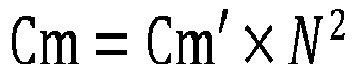
mathematical equation 1 andmathematical equation 2. In the case where the resonance network composed of the inductance element Lm and the capacitance element Cm is not provided at the primary winding of the main isolation transformer, as long as the multiple of the number of turns of the primary winding of the main isolation transformer is set to "N" with respect to the number of turns of primary winding at which the resonance network composed of the inductance element Lm and the capacitance element Cm is located, when the inductance value Lm' and the capacitance value Cm' are calculated by using the above-mentionedmathematical equation 1 andmathematical equation 2, the followingmathematical equation 3 andmathematical equation 4 may be used to calculate the inductance value of the inductance element Lm and the capacitance value of the capacitance element Cm:

- Although the present disclosure has been illustrated above in conjunction with the preferred embodiments of the present disclosure, those skilled in the art can understand that various modifications, substitutions and changes can be made to the disclosure without departing from the technical idea and scope of the disclosure. Therefore, the present disclosure should not be limited by the foregoing embodiments, but should be defined by the appended claims and their equivalents.
Claims (5)
- An LLC converter comprising a resonant network, the resonant network comprising a resonant capacitance element (Cr), a resonant inductance element (Lr), and an excitation inductance unit,
the excitation inductance unit comprising a capacitance element (Cm) and an inductance element (Lm) connected in series,
a minimum operating frequency of the LLC converter being higher than a resonant frequency of the capacitance element (Cm) and the inductance element (Lm). - The LLC converter according to claim 1, wherein:the LLC converter further comprises a main isolation transformer,the excitation inductance unit is provided across a primary winding of the main isolation transformer, a secondary output winding of the main isolation transformer, an additional primary winding of the main isolation transformer, or an additional secondary winding of the main isolation transformer.
- The LLC converter according to claim 1 or 2, wherein:
the LLC converter is a half-bridge LLC converter or a full-bridge LLC converter. - The LLC converter according to claim 2, wherein
letting Cm be a capacitance value of the capacitance element, Lm be an inductance value of the inductance element, Lm_eq_nom be a normal excitation inductance expected for the excitation inductance unit, Lm_eq_min be a minimum excitation inductance expected for the excitation inductance unit, fr be a resonance frequency of the resonance inductance element and the resonance capacitance element, and fsw_min be a minimum operating frequency of the LLC converter, in a case that the excitation inductance unit is provided across the primary winding of the main isolation transformer, the capacitance value of the capacitance element and the inductance value of the inductance element satisfy following relationships:

- The LLC converter according to claim 2, wherein
letting Cm be a capacitance value of the capacitance element, Lm be an inductance value of the inductance element, Lm_eq_nom be a normal excitation inductance expected for the excitation inductance unit, Lm_eq_min be a minimum excitation inductance expected for the excitation inductance unit, fr be a resonance frequency of the resonance inductance element and the resonance capacitance element, and fsw_min be a minimum operating frequency of the LLC converter, in a case that the excitation inductance unit is provided across the secondary output winding of the main isolation transformer, the additional primary winding of the main isolation transformer, or the additional secondary winding of the main isolation transformer, the capacitance value of the capacitance element and the inductance value of the inductance element satisfy following relationships:


Applications Claiming Priority (1)
| Application Number | Priority Date | Filing Date | Title |
|---|---|---|---|
| CN201910278904.3A CN111800013A (en) | 2019-04-08 | 2019-04-08 | LLC converter capable of reducing exciting current and providing high gain |
Publications (1)
| Publication Number | Publication Date |
|---|---|
| EP3723262A1 true EP3723262A1 (en) | 2020-10-14 |
Family
ID=70227872
Family Applications (1)
| Application Number | Title | Priority Date | Filing Date |
|---|---|---|---|
| EP20168504.7A Withdrawn EP3723262A1 (en) | 2019-04-08 | 2020-04-07 | Llc converter that reduces excitation current and is capable of providing high gain |
Country Status (3)
| Country | Link |
|---|---|
| US (1) | US11482939B2 (en) |
| EP (1) | EP3723262A1 (en) |
| CN (1) | CN111800013A (en) |
Families Citing this family (1)
| Publication number | Priority date | Publication date | Assignee | Title |
|---|---|---|---|---|
| CN116232087A (en) * | 2023-03-21 | 2023-06-06 | 深圳市正浩创新科技股份有限公司 | Method and device for determining resonance parameters, electronic equipment and storage medium |
Citations (2)
| Publication number | Priority date | Publication date | Assignee | Title |
|---|---|---|---|---|
| US20140247626A1 (en) | 2012-04-11 | 2014-09-04 | Tai Keung Lee | Hold-up time enhancement circuit for llc resonant converter |
| CN107968471A (en) * | 2017-11-20 | 2018-04-27 | 山东鲁能智能技术有限公司 | LCLC resonance circuits, wide scope constant power output direct current charger and control method |
Family Cites Families (13)
| Publication number | Priority date | Publication date | Assignee | Title |
|---|---|---|---|---|
| US9515562B2 (en) * | 2013-03-05 | 2016-12-06 | Futurewei Technologies, Inc. | LLC resonant converters |
| KR101492964B1 (en) * | 2013-10-15 | 2015-02-24 | 전주대학교 산학협력단 | SLLC Resonant Converter for Bidirectional Power Conversion using auxiliary switches and inductor |
| CN105553272A (en) * | 2015-12-09 | 2016-05-04 | 燕山大学 | Straight-through prevention half-bridge LLC resonance converter |
| US10135348B2 (en) * | 2016-05-13 | 2018-11-20 | Infineon Technologies Austria Ag | LLC power converter and switching method thereof |
| KR102009200B1 (en) * | 2016-07-04 | 2019-08-09 | 숭실대학교산학협력단 | Bidirectional Converter with Auxiliary LC Resonant Circuit and Operating Method thereof |
| US10673323B2 (en) * | 2016-10-27 | 2020-06-02 | University Of Florida Research Foundation, Incorporated | Loop noise balance technique for CM EMI noise reduction of the full bridge LLC resonant converter |
| US20180191168A1 (en) * | 2017-01-04 | 2018-07-05 | National Instruments Corporation | Parallel Interleaved Multiphase LLC Current Sharing Control |
| WO2018140824A1 (en) * | 2017-01-27 | 2018-08-02 | Murata Manufacturing Co., Ltd. | 120-hz ripple reduction with pir controller for llc converter |
| CN106877676B (en) * | 2017-04-06 | 2018-08-07 | 珠海英搏尔电气股份有限公司 | A kind of two-way resonance translation circuit, converter and its control method |
| KR20170104434A (en) * | 2017-09-06 | 2017-09-15 | 서울과학기술대학교 산학협력단 | Resonance-type dc-dc converter |
| CN107612346A (en) * | 2017-09-28 | 2018-01-19 | 西安图为电气技术有限公司 | A kind of two-way DC/DC power inverters |
| CN107809178B (en) * | 2017-11-03 | 2021-06-11 | 上海联影医疗科技股份有限公司 | High-voltage generator and control method thereof |
| CN109361321B (en) * | 2018-11-29 | 2019-10-11 | 西安交通大学 | A reverse working circuit and design method of LLC resonant converter |
-
2019
- 2019-04-08 CN CN201910278904.3A patent/CN111800013A/en not_active Withdrawn
-
2020
- 2020-04-07 EP EP20168504.7A patent/EP3723262A1/en not_active Withdrawn
- 2020-04-08 US US16/843,341 patent/US11482939B2/en active Active
Patent Citations (2)
| Publication number | Priority date | Publication date | Assignee | Title |
|---|---|---|---|---|
| US20140247626A1 (en) | 2012-04-11 | 2014-09-04 | Tai Keung Lee | Hold-up time enhancement circuit for llc resonant converter |
| CN107968471A (en) * | 2017-11-20 | 2018-04-27 | 山东鲁能智能技术有限公司 | LCLC resonance circuits, wide scope constant power output direct current charger and control method |
Also Published As
| Publication number | Publication date |
|---|---|
| US20200321881A1 (en) | 2020-10-08 |
| CN111800013A (en) | 2020-10-20 |
| US11482939B2 (en) | 2022-10-25 |
Similar Documents
| Publication | Publication Date | Title |
|---|---|---|
| Cao et al. | Wide voltage gain range LLC DC/DC topologies: State-of-the-art | |
| US6018468A (en) | Multi-resonant DC-to-DC converter | |
| EP2740206B1 (en) | A resonant-mode power supply with a multi-winding inductor | |
| US20110317452A1 (en) | Bi-directional power converter with regulated output and soft switching | |
| EP3713067B1 (en) | Frequency modulation control for phase-shift full bridge converters | |
| JP2007020391A (en) | Highly efficient half-bridge dc/dc converter and its control method | |
| US20090290384A1 (en) | High power factor isolated buck-type power factor correction converter | |
| US20230113753A1 (en) | Dc/dc converter and method for controlling output voltage thereof | |
| CN108028605A (en) | With the converter for keeping operation | |
| WO2014088708A1 (en) | A hysteretic-mode pulse frequency modulated (hm-pfm) resonant ac to dc converter | |
| KR102308809B1 (en) | A two-stage power conversion converter | |
| US20260005615A1 (en) | Power circuit, power control method, compound power circuit and electronic device | |
| JP2008206224A (en) | Dc converter | |
| WO2020186978A1 (en) | Method for realizing interphase current sharing of illc resonant converter and prolonging power-down hold-up time | |
| TWI747535B (en) | Llc resonance converter, control unit, and method of controlling the same | |
| US12301125B2 (en) | Power converter topology | |
| US20110080757A1 (en) | power converter | |
| Nasiri et al. | A new driving method for a magnetron using a soft switching active clamp fly-back converter | |
| EP3723262A1 (en) | Llc converter that reduces excitation current and is capable of providing high gain | |
| CN101888187A (en) | Control Mode of ZVS Converter at Resonant Operating Frequency | |
| CN114499210A (en) | A control method of high frequency resonant bidirectional isolated DC/DC converter | |
| Naraharisetti | Design of half bridge LLC resonant converter using synchronous rectifier | |
| US10075055B2 (en) | Zero-voltage-switching scheme for phase shift converters | |
| US12362664B2 (en) | Series resonant power converter | |
| US12199505B2 (en) | Llc resonant converter with variable resonant tank |
Legal Events
| Date | Code | Title | Description |
|---|---|---|---|
| PUAI | Public reference made under article 153(3) epc to a published international application that has entered the european phase |
Free format text: ORIGINAL CODE: 0009012 |
|
| STAA | Information on the status of an ep patent application or granted ep patent |
Free format text: STATUS: REQUEST FOR EXAMINATION WAS MADE |
|
| 17P | Request for examination filed |
Effective date: 20200407 |
|
| AK | Designated contracting states |
Kind code of ref document: A1 Designated state(s): AL AT BE BG CH CY CZ DE DK EE ES FI FR GB GR HR HU IE IS IT LI LT LU LV MC MK MT NL NO PL PT RO RS SE SI SK SM TR |
|
| AX | Request for extension of the european patent |
Extension state: BA ME |
|
| STAA | Information on the status of an ep patent application or granted ep patent |
Free format text: STATUS: THE APPLICATION IS DEEMED TO BE WITHDRAWN |
|
| 18D | Application deemed to be withdrawn |
Effective date: 20210415 |