EP3722157A1 - Wiring harness assembly - Google Patents
Wiring harness assembly Download PDFInfo
- Publication number
- EP3722157A1 EP3722157A1 EP20168115.2A EP20168115A EP3722157A1 EP 3722157 A1 EP3722157 A1 EP 3722157A1 EP 20168115 A EP20168115 A EP 20168115A EP 3722157 A1 EP3722157 A1 EP 3722157A1
- Authority
- EP
- European Patent Office
- Prior art keywords
- flexible planar
- wire cable
- wiring harness
- power
- accordance
- Prior art date
- Legal status (The legal status is an assumption and is not a legal conclusion. Google has not performed a legal analysis and makes no representation as to the accuracy of the status listed.)
- Granted
Links
Images




Classifications
-
- B—PERFORMING OPERATIONS; TRANSPORTING
- B60—VEHICLES IN GENERAL
- B60R—VEHICLES, VEHICLE FITTINGS, OR VEHICLE PARTS, NOT OTHERWISE PROVIDED FOR
- B60R16/00—Electric or fluid circuits specially adapted for vehicles and not otherwise provided for; Arrangement of elements of electric or fluid circuits specially adapted for vehicles and not otherwise provided for
- B60R16/02—Electric or fluid circuits specially adapted for vehicles and not otherwise provided for; Arrangement of elements of electric or fluid circuits specially adapted for vehicles and not otherwise provided for electric constitutive elements
- B60R16/0207—Wire harnesses
-
- B—PERFORMING OPERATIONS; TRANSPORTING
- B60—VEHICLES IN GENERAL
- B60R—VEHICLES, VEHICLE FITTINGS, OR VEHICLE PARTS, NOT OTHERWISE PROVIDED FOR
- B60R16/00—Electric or fluid circuits specially adapted for vehicles and not otherwise provided for; Arrangement of elements of electric or fluid circuits specially adapted for vehicles and not otherwise provided for
- B60R16/02—Electric or fluid circuits specially adapted for vehicles and not otherwise provided for; Arrangement of elements of electric or fluid circuits specially adapted for vehicles and not otherwise provided for electric constitutive elements
- B60R16/0207—Wire harnesses
- B60R16/0215—Protecting, fastening and routing means therefor
-
- H—ELECTRICITY
- H01—ELECTRIC ELEMENTS
- H01B—CABLES; CONDUCTORS; INSULATORS; SELECTION OF MATERIALS FOR THEIR CONDUCTIVE, INSULATING OR DIELECTRIC PROPERTIES
- H01B7/00—Insulated conductors or cables characterised by their form
- H01B7/0045—Cable-harnesses
-
- H—ELECTRICITY
- H01—ELECTRIC ELEMENTS
- H01B—CABLES; CONDUCTORS; INSULATORS; SELECTION OF MATERIALS FOR THEIR CONDUCTIVE, INSULATING OR DIELECTRIC PROPERTIES
- H01B13/00—Apparatus or processes specially adapted for manufacturing conductors or cables
- H01B13/012—Apparatus or processes specially adapted for manufacturing conductors or cables for manufacturing wire harnesses
-
- H—ELECTRICITY
- H01—ELECTRIC ELEMENTS
- H01B—CABLES; CONDUCTORS; INSULATORS; SELECTION OF MATERIALS FOR THEIR CONDUCTIVE, INSULATING OR DIELECTRIC PROPERTIES
- H01B7/00—Insulated conductors or cables characterised by their form
- H01B7/04—Flexible cables, conductors, or cords, e.g. trailing cables
-
- H—ELECTRICITY
- H01—ELECTRIC ELEMENTS
- H01B—CABLES; CONDUCTORS; INSULATORS; SELECTION OF MATERIALS FOR THEIR CONDUCTIVE, INSULATING OR DIELECTRIC PROPERTIES
- H01B7/00—Insulated conductors or cables characterised by their form
- H01B7/08—Flat or ribbon cables
-
- H—ELECTRICITY
- H01—ELECTRIC ELEMENTS
- H01B—CABLES; CONDUCTORS; INSULATORS; SELECTION OF MATERIALS FOR THEIR CONDUCTIVE, INSULATING OR DIELECTRIC PROPERTIES
- H01B7/00—Insulated conductors or cables characterised by their form
- H01B7/08—Flat or ribbon cables
- H01B7/0823—Parallel wires, incorporated in a flat insulating profile
-
- H—ELECTRICITY
- H01—ELECTRIC ELEMENTS
- H01B—CABLES; CONDUCTORS; INSULATORS; SELECTION OF MATERIALS FOR THEIR CONDUCTIVE, INSULATING OR DIELECTRIC PROPERTIES
- H01B7/00—Insulated conductors or cables characterised by their form
- H01B7/08—Flat or ribbon cables
- H01B7/0861—Flat or ribbon cables comprising one or more screens
-
- H—ELECTRICITY
- H01—ELECTRIC ELEMENTS
- H01R—ELECTRICALLY-CONDUCTIVE CONNECTIONS; STRUCTURAL ASSOCIATIONS OF A PLURALITY OF MUTUALLY-INSULATED ELECTRICAL CONNECTING ELEMENTS; COUPLING DEVICES; CURRENT COLLECTORS
- H01R12/00—Structural associations of a plurality of mutually-insulated electrical connecting elements, specially adapted for printed circuits, e.g. printed circuit boards [PCB], flat or ribbon cables, or like generally planar structures, e.g. terminal strips, terminal blocks; Coupling devices specially adapted for printed circuits, flat or ribbon cables, or like generally planar structures; Terminals specially adapted for contact with, or insertion into, printed circuits, flat or ribbon cables, or like generally planar structures
- H01R12/50—Fixed connections
- H01R12/59—Fixed connections for flexible printed circuits, flat or ribbon cables or like structures
- H01R12/61—Fixed connections for flexible printed circuits, flat or ribbon cables or like structures connecting to flexible printed circuits, flat or ribbon cables or like structures
-
- H—ELECTRICITY
- H05—ELECTRIC TECHNIQUES NOT OTHERWISE PROVIDED FOR
- H05K—PRINTED CIRCUITS; CASINGS OR CONSTRUCTIONAL DETAILS OF ELECTRIC APPARATUS; MANUFACTURE OF ASSEMBLAGES OF ELECTRICAL COMPONENTS
- H05K3/00—Apparatus or processes for manufacturing printed circuits
- H05K3/36—Assembling printed circuits with other printed circuits
- H05K3/361—Assembling flexible printed circuits with other printed circuits
Definitions
- the signal conductor 24 has a width of less than 2.0mm and a thickness less than about 1.0mm. In the examples illustrated in Figs. 4A-4B , the signal conductor 24 has a width of about 1.54mm, and a thickness of about 0.7mm.
- the dielectric material 34 is the same dielectric material 34 that surrounds the power conductor 22 of Figs 3A-3B , with the thickness adjusted to account for the lack of a shield trace and a shield foil.
- the spacing between the adjacent signal conductors 24 is at least 1.0mm to inhibit the occurrence of crosstalk.
- the three signal conductors 24 are protected from the EMI by a signal electromagnetic shield 36.
- the signal electromagnetic shield 36 includes at least one signal shield trace 38 and at least one signal shield foil 40.
- the dielectric material 34 separates the signal conductors 24 from both the signal shield trace 38 and the signal shield foil 40 to prevent a short circuit from occurring.
- the dielectric material 34 includes adhesive properties to promote bonding between the signal electromagnetic shield 36 and the signal conductor 24.
- a separate adhesive 29 layer is interposed between the dielectric material 34 and the signal conductor 24.
- the thickness of the dielectric material 34 is adjusted based on the dielectric breakdown strength of the dielectric material 34, and a voltage differential between the signal conductor 24 and the signal electromagnetic shield 36. In an example, the thickness of the dielectric material 34 is between about 0.1mm and about 0.5mm. In another example, the thickness of the dielectric material 34 is about 0.4mm. In another example, the thickness of the dielectric material 34 is about 0.075mm.
- the electrical connection 60 is the metallurgical bond and is made within the apertures 54, 58.
- a lateral gap exists between the electrical connection 60 and the surrounding components.
- the gap is filled with the dielectric material 34.
- a wiring harness assembly 10 (the assembly 10), is provided.
- the assembly 10 is an improvement over other wiring harness assemblies because the assembly 10 includes the at least one data conductor 26 configured to transmit network data communications in a flexible planar package, along with the at least one power conductor 22 and the at least one signal conductor 24.
- first contact could be termed a second contact
- second contact could be termed a first contact
- the first contact and the second contact are both contacts, but they are not the same contact.
- the terminology used in the description of the various described embodiments herein is for the purpose of describing particular embodiments only and is not intended to be limiting. As used in the description of the various described embodiments and the appended claims, the singular forms "a”, “an” and “the” are intended to include the plural forms as well, unless the context clearly indicates otherwise. It will also be understood that the term “and/or” as used herein refers to and encompasses any and all possible combinations of one or more of the associated listed items.
- the phrase “if it is determined” or “if [a stated condition or event] is detected” is, optionally, construed to mean “upon determining” or “in response to determining” or “upon detecting [the stated condition or event]” or “in response to detecting [the stated condition or event],” depending on the context.
Landscapes
- Engineering & Computer Science (AREA)
- Manufacturing & Machinery (AREA)
- Mechanical Engineering (AREA)
- Microelectronics & Electronic Packaging (AREA)
- Insulated Conductors (AREA)
Abstract
Description
- This disclosure generally relates to a wiring harness assembly, and more particularly relates to a wiring harness assembly having a flat cable bundle.
- The present invention will now be described, by way of example with reference to the accompanying drawings, in which:
-
Fig. 1 is a perspective view of an illustration of a wiring harness assembly in accordance with one embodiment; -
Fig. 2 is a perspective view of a portion of the wiring harness assembly ofFig. 1 illustrating a cross section of the assembly in accordance with one embodiment; -
Fig. 3A is an illustration of an enlarged cross sectional view of a power conductor portion of the wiring harness assembly ofFig. 1 in accordance with one embodiment; -
Fig. 3B is an illustration of an enlarged cross sectional view of a power conductor portion of the wiring harness assembly ofFig. 1 in accordance with one embodiment; -
Fig. 4A is an illustration of an enlarged cross sectional view of a signal conductor portion of the wiring harness assembly ofFig. 1 in accordance with one embodiment; -
Fig. 4B is an illustration of an enlarged cross sectional view of a signal conductor portion of the wiring harness assembly ofFig. 1 in accordance with one embodiment; -
Fig. 5A is an illustration of an enlarged cross sectional view of a data conductor portion of the wiring harness assembly ofFig. 1 in accordance with one embodiment; -
Fig. 5B is an illustration of an enlarged cross sectional view of a data conductor portion of the wiring harness assembly ofFig. 1 in accordance with one embodiment; -
Fig. 5C is an illustration of an enlarged cross sectional view of a data conductor portion of the wiring harness assembly ofFig. 1 in accordance with one embodiment; -
Fig. 6 is a top perspective view of a portion of a first flexible planar wire cable of the wiring harness assembly ofFig. 1 in accordance with one embodiment; -
Fig. 7 is a bottom view of a portion of a second flexible planar wire cable of the wiring harness assembly ofFig. 1 in accordance with one embodiment; -
Fig. 8 is a section view of an electrical connection of the assembly ofFig. 1 in accordance with one embodiment; -
Fig. 9 is a section view of another electrical connection of the assembly ofFig. 1 in accordance with one embodiment; and -
Fig. 10 is a section view of yet another electrical connection of the assembly ofFig. 1 in accordance with one embodiment. - Reference will now be made in detail to embodiments, examples of which are illustrated in the accompanying drawings. In the following detailed description, numerous specific details are set forth in order to provide a thorough understanding of the various described embodiments. However, it will be apparent to one of ordinary skill in the art that the various described embodiments may be practiced without these specific details. In other instances, well-known methods, procedures, components, circuits, and networks have not been described in detail so as not to unnecessarily obscure aspects of the embodiments.
-
Fig. 1 illustrates a perspective view of awiring harness assembly 10, hereafter referred to as theassembly 10. As will be described in more detail below, theassembly 10 is an improvement over other wiring harness assemblies because theassembly 10 combines electrical power, signal, and data channels in one flexible planar package. In an example, theassembly 10 includes connector bodies attached to ends of theassembly 10 configured to mate with corresponding connector bodies of a vehicle wiring system (not shown). In another example, theassembly 10 includes one or more branches that extend laterally from and/or parallel to theassembly 10. The one or more branches are configured to distribute electrical power, signals, and data to various systems that may be installed on the vehicle. -
Fig. 2 is a perspective view of a portion of theassembly 10 ofFig. 1 illustrating a cross section of theassembly 10. Theassembly 10 includes a first flexibleplanar substrate 12 extending continuously along both alongitudinal axis 14 and alateral axis 16 of theassembly 10. The first flexibleplanar substrate 12 is formed of a polymeric material. The polymeric material may be any polymeric material that electrically isolates portions of the power, signal, and data channels. In one example, the first flexibleplanar substrate 12 is formed of the polymeric material polyethylene naphthalate (PEN). In another example, the first flexibleplanar substrate 12 is formed of the polymeric material polyimide (PI). In yet another example, the first flexibleplanar substrate 12 is formed of the polymeric material polyethylene terephthalate (PET). Other polymeric materials may be selected based on application requirements for electrical isolation (i.e. a dielectric breakdown strength), and/or temperature resistance, and/or mechanical properties (e.g., tensile strength, elongation, abrasion resistance, etc.) of theassembly 10. In an example, the first flexibleplanar substrate 12 has a thickness in a range of 15 micrometers (15µm) to 100 µm and may be adjusted based on a dielectric constant of the polymeric material. In one example, the PEN polymeric material has a thickness of about 25 µm. In another example the PI polymeric material has a thickness of about 75 µm. - The
assembly 10 also includes a second flexibleplanar substrate 18 overlaying the first flexibleplanar substrate 12, extending continuously along both thelongitudinal axis 14 and thelateral axis 16 of theassembly 10. In the example illustrated inFig. 2 , the second flexibleplanar substrate 18 is formed of the same polymeric material as that of the first flexibleplanar substrate 12 described above, and has the same thickness. In another example, the second flexibleplanar substrate 18 is formed of a different polymeric material than that of the first flexibleplanar substrate 12 described above. In yet another example, the second flexibleplanar substrate 18 is has a different thickness than that of the first flexibleplanar substrate 12 described above. - The
assembly 10 also includes a plurality of separated conductors 20 interposed between the first flexibleplanar substrate 12 and the second flexibleplanar substrate 18. In the example illustrated inFig. 2 , the plurality of separated conductors 20 are encapsulated by the first flexibleplanar substrate 12 and the second flexibleplanar substrate 18. In an example, the encapsulation results from a lamination process of the first flexibleplanar substrate 12 and the second flexibleplanar substrate 18 by applying heat and pressure to opposing surfaces of the first flexibleplanar substrate 12 and the second flexibleplanar substrate 18, thereby joining the first flexibleplanar substrate 12 and the second flexibleplanar substrate 18 together. In an example, an adhesive 29 is also interposed between the first flexibleplanar substrate 12 and the second flexibleplanar substrate 18. It will be appreciated that the lamination process results in a seal at an interface between the first flexibleplanar substrate 12 and the second flexibleplanar substrate 18 that inhibits moisture intrusion. In an example, the first flexibleplanar substrate 12 and the second flexibleplanar substrate 18 are urged into spaces between the plurality of separated conductors 20 during the lamination process to create a dielectric barrier between the plurality of separated conductors 20. - The plurality of separated conductors 20 include at least one
power conductor 22 configured to transmit electrical power, at least onesignal conductor 24 configured to transmit electrical signals, and at least onedata conductor 26 configured to transmit network data communications. Thepower conductor 22,signal conductor 24, anddata conductor 26 may be arranged in any order along thelateral axis 16 of theassembly 10. In the example illustrated inFig. 2 , thepower conductor 22 anddata conductor 26 are arranged proximate the opposing edges of theassembly 10, with thesignal conductor 24 disposed between thepower conductor 22 anddata conductor 26. - As used herein, transmission of electrical power includes the transmission of electrons where a voltage is typically greater than about five volts (5V), and an electrical current is typically greater than about one ampere (1A). For example, a
typical power conductor 22 in a vehicle may supply electrical power at battery voltage (i.e. 14V to 48V), and current at 15A to 30A. As used herein, transmission of electrical signals include the transmission of electrons where the voltage is typically less than about 5V, and the current is typically less than about 5A. For example, atypical signal conductor 24 in a vehicle, used for switching a component on and off (e.g., electric door locks), may transmit electrical signals between about 0.0V and about 5V, and the current between about 0.0A and about 0.1A. In another example, the transmission of electrical signals includes a voltage-based state where a 0.0V signal denotes a "low" logic value (i.e. logical zero) and a full scale signal (e.g. 5V) denotes a "high" logic value (i.e. logical one). As used herein, transmission of network data communications include the transmission of electrons where the voltage is typically less than about 5V, and the current is typically less than about 0.1A. For example, atypical data conductor 26 in a vehicle, such as a Computer Area Network (CAN)data conductor 26 used to send messages between various vehicle controllers and/or between vehicle controllers and electrical components, may transmit electrical signals between about 0.0V and about 5V, and current between about 0.0A and about 0.05A. In an example, the data communications are digital bit streams having a predetermined bit timing and structure. In the example illustrated inFig. 2 , thedata conductor 26 further includes a pair of continuous strips of electrically conductive material (i.e. a data pair), such as copper, aluminum, silver, gold, or alloys thereof. In this example, the data pair enable the use of a differential voltage between the data pair as part of a message protocol. In an example, data transmission rates (i.e. baud rates) reach in excess of 1 million bits per second (1Mbps). - In the example illustrated in
Fig. 2 , a spacing between thepower conductor 22 and theadjacent signal conductor 24 is at least 1.0mm, and the spacing between thesignal conductor 24 and theadjacent data conductor 26 is at least 1.0mm. The spacing between the adjacent plurality of separated conductors 20 are maintained at these values to provide adequate electrical isolation between the conductors to inhibit short circuits, and/or to inhibit crosstalk of the transmitted electrical signals. Crosstalk is a phenomenon in electronics where a signal transmitted on one wire or channel, creates an interference in another wire or channel. Crosstalk is a form of electromagnetic interference (EMI) that is caused by a magnetic field generated around a wire that is transmitting electrical current. The magnetic field from an interfering circuit may induce an electrical current in a nearby circuit creating electrical noise or interference. - In an example, the
power conductor 22 comprises a single continuous strip of electrically conductive material, such as copper, aluminum, silver, gold, or alloys thereof. In another example, the electrically conductive material includes a conductive coating, such as tin or a tin alloy, to inhibit corrosion. In the example illustrated inFig. 2 , thepower conductor 22 has a width greater than thesignal conductor 24 and greater than thedata conductor 26, the benefits of which will be described in more detail below. In order for thepower conductor 22 to transmit the desired electrical power described above, an electrical resistance is kept to a minimum by adjusting a cross sectional area of thepower conductor 22. In an example, thepower conductor 22 has a width greater than 1mm and a thickness less than about 1.0mm. In another example, thepower conductor 22 has a width of about 10mm, and a thickness of about 0.125mm. In the example illustrated inFig. 2 , thepower conductor 22 has a width of about 10mm, and a thickness of about 0.7mm. -
Figs. 3A-3B illustrate examples of an enlarged cross sectional view of thepower conductor 22 portion of theassembly 10. In these examples, thepower conductor 22 is located proximate an edge of theassembly 10. In an example, a distance between a first side of thepower conductor 22 and a first edge of the first flexibleplanar substrate 12 is about 2mm. Theassembly 10 further includes a powerelectromagnetic shield 28 surrounding thepower conductor 22. The powerelectromagnetic shield 28 is configured to inhibit EMI from affecting thenearby signal conductors 24,data conductors 26, and/or other electrical components proximate theassembly 10. The EMI is generated by the magnetic field that surrounds thepower conductor 22 that is created when the electrical power is transmitted through thepower conductor 22. Electromagnetic shielding provides an electrically conductive barrier to attenuate (i.e., reduce) electromagnetic waves external to the shield, and provides a conduction path by which any induced electrical currents can be circulated and returned to the source by way of an electrical ground connection to the shield (not shown). As illustrated inFigs. 3A-3B , an adhesive 29 is interposed between the powerelectromagnetic shield 28 and both the first flexibleplanar substrate 12 and the second flexibleplanar substrate 18. This adhesive 29 has the benefit of inhibiting a relative motion between the powerelectromagnetic shield 28 and both the first flexibleplanar substrate 12 and the second flexibleplanar substrate 18, that may cause damage to the powerelectromagnetic shield 28. In an example, the adhesive 29 also includes dielectric properties. - The power
electromagnetic shield 28 includes at least onepower shield trace 30 and at least onepower shield foil 32, wherein thepower shield trace 30 and thepower shield foil 32 are in electrical contact in order to create a continuous shield. In the example illustrated inFig. 3A , the powerelectromagnetic shield 28 terminates without wrapping around the side of thepower conductor 22. This shielding arrangement provides sufficient EMI reduction when thepower conductor 22 is located proximate the edge of theassembly 10, and theassembly 10 is not routed near any electronic devices that may require protection from EMI. In an example, a spacing between thepower shield trace 30 and thepower conductor 22 is about 1mm. In an example, the thickness of thepower shield trace 30 matches the thickness of thepower conductor 22. In another example, the thickness of thepower shield trace 30 is greater than the thickness of thepower conductor 22. In an example the thickness of thepower shield foil 32 is between 0.01mm and 0.04mm. - Both the
power shield trace 30 and thepower shield foil 32 are formed of continuous strips of electrically conductive material, such as copper, aluminum, silver, gold, or alloys thereof. In an example, thepower shield trace 30 and thepower shield foil 32 includes a conductive coating, such as tin or a tin alloy, to inhibit corrosion. In an example, thepower shield trace 30 and thepower shield foil 32 are formed of the same electrically conductive material as that of thepower conductor 22. In another example, thepower shield trace 30 and thepower shield foil 32 are formed of a different electrically conductive material than that of thepower conductor 22. -
Fig. 3B illustrates an example where anotherpower shield trace 30 is located along the first side of thepower conductor 22, separating thepower conductor 22 and the first edge of the first flexibleplanar substrate 12. In this example, the powerelectromagnetic shield 28 completely surrounds thepower conductor 22. It will be appreciated that this shielding arrangement provides additional EMI shielding compared to that ofFig. 3A . While the example illustrated inFig. 3B includes separate power shield foils 32 (i.e., an upper foil and a lower foil) individually attached to the first and second power shield traces 30, other arrangements of thepower shield trace 30 andpower shield foil 32 are envisioned, but not shown, such as a singlepower shield foil 32 that completely surrounds thepower conductor 22, overlapping itself to create the continuous shield. In another example not shown, a singlepower shield foil 32 extends from a top side of a singlepower shield trace 30 and returns to a bottom side of the singlepower shield trace 30, completely surrounding thepower conductor 22. - Referring again to
Figs 3A-3B , adielectric material 34 separates thepower conductor 22 from both thepower shield trace 30 and thepower shield foil 32 to prevent a short circuit from occurring. It will be appreciated that the short circuit between thepower conductor 22 and the powerelectromagnetic shield 28 will make the EMI shielding ineffective. Thedielectric material 34 that separates thepower conductor 22 and the powerelectromagnetic shield 28 may be anydielectric material 34 that is compatible with the requirements of the assembly 10 (e.g., dielectric breakdown strength, flexibility, etc.). One suchdielectric material 34 is the RT/DUROID ® 5880 from Rogers Corporation of Chandler, Arizona, USA. In an example, thedielectric material 34 includes adhesive properties to promote bonding between the powerelectromagnetic shield 28 and thepower conductor 22. In another example, a separate adhesive 29 layer is interposed between thedielectric material 34 and thepower conductor 22. The thickness of thedielectric material 34 is adjusted based on the dielectric breakdown strength of thedielectric material 34, and a voltage differential between thepower conductor 22 and the powerelectromagnetic shield 28. In an example, the thickness of thedielectric material 34 is between about 0.1mm and about 0.5mm. In another example, the thickness of thedielectric material 34 is about 0.4mm. In another example, the thickness of thedielectric material 34 is about 0.075mm. - In an example, the
assembly 10 includes a plurality ofpower conductors 22 arranged parallel to one another along thelongitudinal axis 14 of theassembly 10. In an example, a spacing betweenadjacent power conductors 22 is at least 1.0mm. In an example, the plurality ofpower conductors 22 are surrounded by the single powerelectromagnetic shield 28 with thedielectric material 34 separating the plurality ofpower conductors 22 from the single powerelectromagnetic shield 28. In another example, the plurality ofpower conductors 22 are individually surrounded by a plurality of powerelectromagnetic shields 28 with thedielectric material 34 separating theindividual power conductors 22 from the corresponding powerelectromagnetic shield 28. -
Figs. 4A-4B illustrate examples of an enlarged cross sectional view of thesignal conductor 24 portion of theassembly 10, showing threeseparate signal conductors 24. It will be appreciated that any number ofsignal conductors 24 may be included within theassembly 10 to meet the requirements of the vehicle electrical system. In an example, thesignal conductor 24 comprises a single continuous strip of electrically conductive material, such as copper, aluminum, silver, gold, or alloys thereof. In another example, the electrically conductive material includes a conductive coating, such as tin or a tin alloy, to inhibit corrosion. Thesignal conductor 24 is not configured to transmit the same levels of electrical power as that of thepower conductor 22, and does not have the same cross sectional area as thepower conductor 22 to achieve the desired electrical resistance. In an example, thesignal conductor 24 has a width of less than 2.0mm and a thickness less than about 1.0mm. In the examples illustrated inFigs. 4A-4B , thesignal conductor 24 has a width of about 1.54mm, and a thickness of about 0.7mm. - Referring to
Fig. 4A , threeunshielded signal conductors 24 are surrounded by thedielectric material 34. In this example, theunshielded signal conductors 24 are protected from the EMI of theadjacent power conductor 22 by the powerelectromagnetic shield 28. In this example, thedielectric material 34 is the samedielectric material 34 that surrounds thepower conductor 22 ofFigs 3A-3B , with the thickness adjusted to account for the lack of a shield trace and a shield foil. In an example, the spacing between theadjacent signal conductors 24 is at least 1.0mm to inhibit the occurrence of crosstalk. - In another example illustrated in
Fig. 4B , the threesignal conductors 24 are protected from the EMI by a signalelectromagnetic shield 36. The signalelectromagnetic shield 36 includes at least onesignal shield trace 38 and at least onesignal shield foil 40. In an example, thedielectric material 34 separates thesignal conductors 24 from both thesignal shield trace 38 and thesignal shield foil 40 to prevent a short circuit from occurring. In an example, thedielectric material 34 includes adhesive properties to promote bonding between the signalelectromagnetic shield 36 and thesignal conductor 24. In another example, a separate adhesive 29 layer is interposed between thedielectric material 34 and thesignal conductor 24. The thickness of thedielectric material 34 is adjusted based on the dielectric breakdown strength of thedielectric material 34, and a voltage differential between thesignal conductor 24 and the signalelectromagnetic shield 36. In an example, the thickness of thedielectric material 34 is between about 0.1mm and about 0.5mm. In another example, the thickness of thedielectric material 34 is about 0.4mm. In another example, the thickness of thedielectric material 34 is about 0.075mm. -
Figs. 5A-5C illustrate three examples of an enlarged cross sectional view of thedata conductor 26 portion of theassembly 10, showing a pair of continuous strips of conductive material, hereafter referred to as a data pair. In an example, the data pair is formed of continuous strips of electrically conductive material, such as copper, aluminum, silver, gold, or alloys thereof. In another example, the electrically conductive material includes a conductive coating, such as tin or a tin alloy, to inhibit corrosion. Like thesignal conductor 24, thedata conductor 26 is not configured to transmit the same levels of electrical power as that of thepower conductor 22, and does not have the same cross sectional area as thepower conductor 22 to achieve the desired electrical resistance. In an example, the individual traces of thedata conductor 26 have the width of less than 0.5mm and the thickness less than about 1.0mm. In the examples illustrated inFigs. 5A-5C , the individual traces of thedata conductor 26 have the width of about 0.3mm, and the thickness of about 0.7mm. Additionally, the spacing (i.e., spacing along thelongitudinal axis 14,lateral axis 16, and vertical axis) between individual traces of thedata conductor 26 are at least 0.3mm to inhibit crosstalk between the individual traces. -
Fig. 5A illustrates the data pair of adata conductor 26A that are parallel and coplanar (i.e., side-by-side conductors in a same plane).Fig. 5B illustrates the data pair of a data conductor 26B that are parallel and lay in separate parallel planes (i.e., over-under conductors in different planes).Fig. 5C illustrates the data pair of a data conductor 26C that are a twisted pair that alternate between separate planes at regular intervals (i.e., a twist rate, pitch of the twist, etc.). The twisted pair is a type of wiring arrangement that reduces electromagnetic radiation from the pair of conductors, reduces crosstalk between adjacent pairs of conductors, and improves a rejection of any external EMI. In theplanar assembly 10, the twist in the data conductors 26C is accomplished by vertical connections made to alternating short segments of the data conductors 26C disposed on separate parallel planes. The alternating short segments form a crisscross pattern when viewed along the vertical axis, which creates the twisted arrangement. - In the three examples illustrated in
Figs. 5A-5C , the conductors are separated from one another by thedielectric material 34 that is the samedielectric material 34 described above inFigs. 3A-4B . In these examples, the thickness of thedielectric material 34 is adjusted based on the thickness of thedata conductors 26. - Referring again to
Figs. 5A-5C , theassembly 10 further includes a dataelectromagnetic shield 42 to protect thedata conductor 26 from EMI. The dataelectromagnetic shield 42 includes at least onedata shield trace 44 and at least onedata shield foil 46. In an example, thedielectric material 34 separates thedata conductors 26 from both thedata shield trace 44 and thedata shield foil 46 to prevent a short circuit from occurring. In an example, thedielectric material 34 includes adhesive properties to promote bonding between the dataelectromagnetic shield 42 and thedata conductor 26. In another example, a separate adhesive 29 layer is interposed between thedielectric material 34 and thedata conductor 26. The thickness of thedielectric material 34 is adjusted based on the dielectric breakdown strength of thedielectric material 34, and a voltage differential between thesignal conductor 24 and the dataelectromagnetic shield 42, and/or the voltage differential between the data pair. In an example, the thickness of thedielectric material 34 is between about 0.1mm and about 0.5mm. In another example, the thickness of thedielectric material 34 is about 0.4mm. In another example, the thickness of thedielectric material 34 is about 0.075mm. In yet another example, the thickness of thedielectric material 34 between the data pair is at least 0.3mm. - Referring back to
Fig. 1 , theassembly 10 includes a first flexibleplanar wire cable 48 having a first plurality of separated conductors 20A formed in a first insulating layer. Theassembly 10 also includes at least one second flexibleplanar wire cable 50 having a second plurality of separated conductors 20B formed in a second insulating layer. In an example, the first flexibleplanar wire cable 48 and the at least one second flexibleplanar wire cable 50 are initially formed as part of a single flexible planar wire cable that is sectioned to create separate lengths of cable. In the example illustrated inFig. 1 , the first insulating layer and the second insulating layer are formed of the first flexibleplanar substrate 12, the second flexibleplanar substrate 18, thedielectric material 34, and the adhesive 29, that together insulate portions of the first plurality of separated conductors 20A and the second plurality of separated conductors 20B. In an example, the at least one second flexibleplanar wire cable 50 extends from the first flexibleplanar wire cable 48 in a direction obtuse to thelongitudinal axis 14 of the first flexibleplanar wire cable 48. In another example, the at least one second flexibleplanar wire cable 50 extends from the first flexibleplanar wire cable 48 in a direction parallel to thelongitudinal axis 14 of the first flexibleplanar wire cable 48. In the example illustrated inFig. 1 , the at least one second flexibleplanar wire cable 50 extends from the first flexibleplanar wire cable 48 in a direction orthogonal to the longitudinal axis14 of the first flexible planar wire cable 48 (i.e., along thelateral axis 16 of the assembly 10). - In an example, the first plurality of separated conductors 20A include a first at least one
power conductor 22A surrounded by a first power electromagnetic shield 28A, a first at least one signal conductor 24A surrounded by a first signal electromagnetic shield 36A, and a first at least one data conductor 26D surrounded by a first data electromagnetic shield 42A. The second plurality of separated conductors 20B include a second at least onepower conductor 22B surrounded by a second power electromagnetic shield 28B, a second at least one signal conductor 24B surrounded by a second signal electromagnetic shield 36B, and a second at least one data conductor 26E surrounded by a second data electromagnetic shield 42B. - In another example, the first plurality of separated conductors 20A include the first at least one
power conductor 22A surrounded by the first power electromagnetic shield 28A, the first at least one signal conductor 24A that is unshielded, and the first at least one data conductor 26D surrounded by the first data electromagnetic shield 42A. The second plurality of separated conductors 20B include a second at least onepower conductor 22B surrounded by a second power electromagnetic shield 28B, a second at least one signal conductor 24B that is unshielded, and a second at least one data conductor 26E surrounded by a second data electromagnetic shield 42B. -
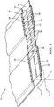
Fig. 6 illustrates a portion of the first flexibleplanar wire cable 48 isolated from theassembly 10 ofFig. 1 . The first insulating layer includes a first substantially flatexterior surface 52 that defines a first plurality ofapertures 54. The first plurality ofapertures 54 expose at least a portion of the one or more of the first plurality of separated conductors 20A and/or first electromagnetic shields. In an example, the exposed portions of each of the first plurality of separated conductors 20A and/or first electromagnetic shields include a coating of conductive material, such as a tin plating or tin alloy plating. The first plurality ofapertures 54 are arranged in clusters (i.e., bunches, groups, collections, bands, etc.) along thelongitudinal axis 14 of the first flexibleplanar wire cable 48. In an example, the clusters are repeated at a predetermined interval along thelongitudinal axis 14 of the first flexibleplanar wire cable 48. That is, the clusters of the first plurality ofapertures 54 are repeated at regular intervals along a length of the first flexibleplanar wire cable 48, the purpose of which will be explained below. - The first plurality of
apertures 54 are sized, shaped, and arranged such that arranging a second substantially flatexterior surface 56 of the second flexibleplanar wire cable 50 in contact with the first substantially flatexterior surface 52 enables anelectrical connection 60 between the at least one second flexibleplanar wire cable 50 and the first flexibleplanar wire cable 48. It will be appreciated that the second substantially flatexterior surface 56 of the second flexibleplanar wire cable 50 is the surface that is defined by the first flexibleplanar substrate 12, while the first substantially flatexterior surface 52 is the surface that is defined by the second flexibleplanar substrate 18. In the example illustrated inFig. 6 , the first plurality ofapertures 54 within the clusters are arranged in a staggered pattern relative to one another along thelongitudinal axis 14 of the first flexibleplanar wire cable 48. The staggered pattern of the first plurality ofapertures 54 enables theelectrical connection 60 between one or more of the first plurality of separated conductors 20A and one or more of the second plurality of separated conductors 20B and/or between the first electromagnetic shields and the second electromagnetic shields. -
Fig. 7 illustrates a bottom view of a portion of the second flexibleplanar wire cable 50 isolated from theassembly 10 ofFig. 1 . The second substantially flatexterior surface 56 of the second flexibleplanar wire cable 50 defines a second plurality ofapertures 58 that expose at least a portion of one or more of the second plurality of separated conductors 20B and/or second electromagnetic shields. In an example, the exposed portions of each of the second plurality of separated conductors 20B and/or first electromagnetic shields include a coating of conductive material, such as a tin plating or tin alloy plating. The second plurality ofapertures 58 are sized, shaped, and arranged to overlay the first plurality ofapertures 54 to enable theelectrical connections 60. In an example, the second plurality ofapertures 58 are arranged in clusters along thelongitudinal axis 14 of the second flexibleplanar wire cable 50. In the example illustrated inFig. 1 , thelongitudinal axis 14 of the second flexibleplanar wire cable 50 is aligned with thelateral axis 16 of theassembly 10. In an example, the clusters are repeated at a predetermined interval along thelongitudinal axis 14 of the second flexibleplanar wire cable 50. In the example illustrated inFig. 1 , only a single cluster of the second plurality ofapertures 58 exists to make theelectrical connection 60 between the second flexibleplanar wire cable 50 and the first flexibleplanar wire cable 48. In the example illustrated inFig. 7 , the second plurality ofapertures 58 within the cluster are arranged in the staggered pattern relative to one another along thelongitudinal axis 14 of the second flexibleplanar wire cable 50. The staggered pattern of the second plurality ofapertures 58 enables theelectrical connection 60 between one or more of the first plurality of separated conductors 20A and one or more of the second plurality of separated conductors 20B and/or between the first electromagnetic shields and the second electromagnetic shields. -
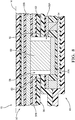
Fig. 8 illustrates an example of abond 62 between the first flexibleplanar wire cable 48 and the second flexibleplanar wire cable 50. For the purposes of illustration, a section view of thepower conductor 22 portion of theassembly 10 is shown, and the description below will apply to thebonds 62 between the other portions of theassembly 10. In an example, thebonds 62 between the first substantially flatexterior surface 52 and the second substantially flatexterior surface 56 are located proximate a perimeter of each of the first plurality ofapertures 54 and each of the second plurality ofapertures 58. In an example, thebond 62 is achieved with an adhesive, such as an epoxy or silicone rubber. In an example, thebond 62 is achieved through localized heating of the first substantially flatexterior surface 52 and the second substantially flatexterior surface 56. In another example, thebond 62 is achieved by a chemical solvent that assists in a crosslinking between the first substantially flatexterior surface 52 and the second substantially flatexterior surface 56. In an example, thebond 62 exists along the full length of contact between the first substantially flatexterior surface 52 and the second substantially flatexterior surface 56. -
Fig. 8 also illustrates an example of theelectrical connection 60 between the first flexibleplanar wire cable 48 and the second flexibleplanar wire cable 50. In an example, theelectrical connections 60 between the one or more of the first plurality of separated conductors 20A and the one or more of the second plurality of separated conductors 20B is a metallurgical bond. In an example, the metallurgical bond is a weld joint from a high frequency weld, or a resistance weld. In another example, the metallurgical bond is a solder joint. In an example, theelectrical connections 60 between the one or more of the first plurality of separated conductors 20A and the one or more of the second plurality of separated conductors 20B is a mechanical bond enabled by a compressive fitting applied to opposing surfaces of both the first flexibleplanar wire cable 48 and the second flexibleplanar wire cable 50. In another example, the mechanical bond is enabled by a staking operation between the first flexibleplanar wire cable 48 and the second flexibleplanar wire cable 50. - Referring again to
Fig. 8 , in this example the first at least onepower conductor 22A of the first plurality of separated conductors 20A is electrically connected to the second at least onepower conductor 22B of the second plurality of separated conductors 20B. It will be understood that the example illustrated inFig. 8 , and the description below, will also apply to the electrical connections 60 (not shown) between the first at least one signal conductor 24A and the second at least one signal conductor 24B, as well as the electrical connections 60 (not shown) between the first at least one data conductor 26D and the second at least one data conductor 26E. In an example, theelectrical connections 60 between the first at least one data conductor 26D and the second at least one data conductor 26E illustrated inFig. 5B are enabled by lateral offset conductors (not specifically shown) that create lateral connection points for the superimposeddata conductors 26. - In the example illustrated in
Fig. 8 , theelectrical connection 60 is the metallurgical bond. Theelectrical connection 60 is made within theapertures power conductors Fig. 8 , a lateral gap exists between theelectrical connection 60 and the surrounding components. In another example, the gap is filled with thedielectric material 34 to inhibit short circuits. A dimension of the gap and/or thedielectric material 34 within the gap is adjusted based on the voltage differential between thepower conductors -
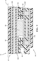
Fig. 9 illustrates theelectrical connection 60 between the one or more first electromagnetic shields of the first plurality of separated conductors 20A and the one or more second electromagnetic shields of the second plurality of separated conductors 20B. In this example, a firstpower shield foil 32A of the first plurality of separated conductors 20A is electrically connected to a secondpower shield foil 32B of the second plurality of separated conductors 20B. It will be understood that the example illustrated inFig. 9 , and the description below, will also apply to the electrical connections 60 (not shown) between a first signal shield foil 40A and a second signal shield foil 40B, as well as the electrical connections 60 (not shown) between a first data shield foil 46A and a second data shield foil 46B. In the example illustrated inFig. 9 , theelectrical connection 60 is the metallurgical bond and is made within theapertures Fig. 9 , a lateral gap exists between theelectrical connection 60 and the surrounding components. In another example, the gap is filled with thedielectric material 34. -
Fig. 10 illustrates another example of theelectrical connection 60 between the one or more first electromagnetic shields of the first plurality of separated conductors 20A and the one or more second electromagnetic shields of the second plurality of separated conductors 20B. In this example, a firstpower shield trace 30A of the first plurality of separated conductors 20A is electrically connected to a secondpower shield trace 30B of the second plurality of separated conductors 20B. It will be understood that the example illustrated inFig. 10 , and the description below, will also apply to the electrical connections 60 (not shown) between a first signal shield trace 38A and a second signal shield trace 38B, as well as the electrical connections 60 (not shown) between a first data shield trace 44A and a second data shield trace 44B. In the example illustrated inFig. 10 , theelectrical connection 60 is the metallurgical bond and is made within theapertures Fig. 10 , a lateral gap exists between theelectrical connection 60 and the surrounding components. In another example, the gap is filled with thedielectric material 34. - Accordingly, a wiring harness assembly 10 (the assembly 10), is provided. The
assembly 10 is an improvement over other wiring harness assemblies because theassembly 10 includes the at least onedata conductor 26 configured to transmit network data communications in a flexible planar package, along with the at least onepower conductor 22 and the at least onesignal conductor 24. - Although the present disclosure is not so limited, the following numbered examples demonstrate one or more aspects of the disclosure.
- Example 1. A wiring harness assembly, comprising: a first flexible planar wire cable having a first plurality of separated conductors formed in a first insulating layer comprising a first substantially flat exterior surface; the first substantially flat exterior surface defining a first plurality of apertures that expose at least a portion of one or more of the first plurality of separated conductors; wherein the first plurality of apertures are sized, shaped, and arranged such that arranging a second substantially flat exterior surface of a second flexible planar wire cable in contact with the first substantially flat exterior surface enables an electrical connection between one or more of the first plurality of separated conductors of the first flexible planar wire cable and one or more of a second plurality of separated conductors formed in a second insulating layer of the second flexible planar wire cable.
- Example 2. The wiring harness assembly in accordance with example 1, wherein the first plurality of apertures are arranged in clusters along a longitudinal axis of the first flexible planar wire cable.
- Example 3. The wiring harness assembly in accordance with example 2, wherein the clusters are repeated at a predetermined interval along the longitudinal axis of the first flexible planar wire cable.
- Example 4. The wiring harness assembly in accordance with example 2, wherein the first plurality of apertures within the clusters are arranged in a staggered pattern relative to one another along the longitudinal axis of the first flexible planar wire cable.
- Example 5. The wiring harness assembly in accordance with any one of the preceding examples, wherein at least one second flexible planar wire cable is electrically connected to the first flexible planar wire cable.
- Example 6. The wiring harness assembly in accordance with example 5, wherein the second substantially flat exterior surface of the second flexible planar wire cable defines a second plurality of apertures that expose at least a portion of one or more of the second plurality of separated conductors; the second plurality of apertures sized, shaped, and arranged to overlay the first plurality of apertures.
- Example 7. The wiring harness assembly in accordance with example 6, wherein the second plurality of apertures are arranged in clusters along a longitudinal axis of the second flexible planar wire cable.
- Example 8. The wiring harness assembly in accordance with example 7, wherein the clusters are repeated at a predetermined interval along the longitudinal axis of the second flexible planar wire cable.
- Example 9. The wiring harness assembly in accordance with example 7, wherein the second plurality of apertures within the clusters are arranged in a staggered pattern relative to one another along the longitudinal axis of the second flexible planar wire cable.
- Example 10. The wiring harness assembly in accordance with example 6, wherein the first substantially flat exterior surface is bonded to the second substantially flat exterior surface.
- Example 11. The wiring harness assembly in accordance with example 5, further comprising: the electrical connection between one or more first electromagnetic shield of the first plurality of separated conductors and one or more second electromagnetic shield of the second plurality of separated conductors.
- Example 12. The wiring harness assembly in accordance with example 11, wherein the one or more first electromagnetic shield comprise a first power electromagnetic shield.
- Example 13. The wiring harness assembly in accordance with example 11, wherein the one or more first electromagnetic shield comprise a first signal electromagnetic shield.
- Example 14. The wiring harness assembly in accordance with example 11, wherein the one or more first electromagnetic shield comprise a first data conductor shield.
- Example 15. The wiring harness assembly in accordance with example 11, wherein the one or more second electromagnetic shield comprise a second power electromagnetic shield.
- Example 16. The wiring harness assembly in accordance with example 11, wherein the one or more second electromagnetic shield comprise a second signal conductor shield.
- Example 17. The wiring harness assembly in accordance with example 11, wherein the one or more second electromagnetic shield comprise a second data conductor shield.
- Example 18. The wiring harness assembly in accordance with any one of the preceding examples, wherein the first plurality of separated conductors comprise: a first at least one power conductor configured to transmit electrical power; a first at least one signal conductor configured to transmit electrical signals; and a first at least one data conductor configured to transmit network data communications.
- Example 19. The wiring harness assembly in accordance with example 18, wherein the second plurality of separated conductors comprise: a second at least one power conductor configured to transmit the electrical power; a second at least one signal conductor configured to transmit the electrical signals; and a second at least one data conductor configured to transmit the network data communications.
- 20. The wiring harness assembly in accordance with example 19, wherein the first at least one power conductor of the first plurality of separated conductors is electrically connected to the second at least one power conductor of the second plurality of separated conductors.
- Example 21. The wiring harness assembly in accordance with example 19, wherein the first at least one signal conductor of the first plurality of separated conductors is electrically connected to the second at least one signal conductor of the second plurality of separated conductors.
- Example 22. The wiring harness assembly in accordance with example 19, wherein the first at least one data conductor of the first plurality of separated conductors is electrically connected to the second at least one data conductor of the second plurality of separated conductors.
- While this invention has been described in terms of the preferred embodiments thereof, it is not intended to be so limited, but rather only to the extent set forth in the claims that follow. "One or more" includes a function being performed by one element, a function being performed by more than one element, e.g., in a distributed fashion, several functions being performed by one element, several functions being performed by several elements, or any combination of the above. It will also be understood that, although the terms first, second, etc. are, in some instances, used herein to describe various elements, these elements should not be limited by these terms. These terms are only used to distinguish one element from another. For example, a first contact could be termed a second contact, and, similarly, a second contact could be termed a first contact, without departing from the scope of the various described embodiments. The first contact and the second contact are both contacts, but they are not the same contact. The terminology used in the description of the various described embodiments herein is for the purpose of describing particular embodiments only and is not intended to be limiting. As used in the description of the various described embodiments and the appended claims, the singular forms "a", "an" and "the" are intended to include the plural forms as well, unless the context clearly indicates otherwise. It will also be understood that the term "and/or" as used herein refers to and encompasses any and all possible combinations of one or more of the associated listed items. It will be further understood that the terms "includes," "including," "comprises," and/or "comprising," when used in this specification, specify the presence of stated features, integers, steps, operations, elements, and/or components, but do not preclude the presence or addition of one or more other features, integers, steps, operations, elements, components, and/or groups thereof. As used herein, the term "if' is, optionally, construed to mean "when" or "upon" or "in response to determining" or "in response to detecting," depending on the context. Similarly, the phrase "if it is determined" or "if [a stated condition or event] is detected" is, optionally, construed to mean "upon determining" or "in response to determining" or "upon detecting [the stated condition or event]" or "in response to detecting [the stated condition or event]," depending on the context.
Claims (15)
- A wiring harness assembly (10), comprising:a first flexible planar wire cable (48) having a first plurality of separated conductors (20) formed in a first insulating layer comprising a first substantially flat exterior surface (52);the first substantially flat exterior surface (52) defining a first plurality of apertures (54) that expose at least a portion of one or more of the first plurality of separated conductors (20);wherein the first plurality of apertures (54) are sized, shaped, and arranged such that arranging a second substantially flat exterior surface (52) of a second flexible planar wire cable (50) in contact with the first substantially flat exterior surface (52) enables an electrical connection (60) between one or more of the first plurality of separated conductors (20) of the first flexible planar wire cable (48) and one or more of a second plurality of separated conductors (20) formed in a second insulating layer of the second flexible planar wire cable (50).
- The wiring harness assembly (10) in accordance with claim 1, wherein the first plurality of apertures (54) are arranged in clusters along a longitudinal axis (14) of the first flexible planar wire cable (48).
- The wiring harness assembly (10) in accordance with claim 2, wherein the clusters are repeated at a predetermined interval along the longitudinal axis (14) of the first flexible planar wire cable (48).
- The wiring harness assembly (10) in accordance with claim 2 or 3, wherein the first plurality of apertures (54) within the clusters are arranged in a staggered pattern relative to one another along the longitudinal axis (14) of the first flexible planar wire cable (48).
- The wiring harness assembly (10) in accordance with any one of the preceding claims, wherein at least one second flexible planar wire cable (50) is electrically connected to the first flexible planar wire cable (48).
- The wiring harness assembly (10) in accordance with claim 5,wherein the second substantially flat exterior surface (52) of the second flexible planar wire cable (50) defines a second plurality of apertures (54) that expose at least a portion of one or more of the second plurality of separated conductors (20); andwherein the second plurality of apertures (54) are sized, shaped, and arranged to overlay the first plurality of apertures (54).
- The wiring harness assembly (10) in accordance with claim 6, wherein the second plurality of apertures (54) are arranged in clusters along a longitudinal axis (14) of the second flexible planar wire cable (50).
- The wiring harness assembly (10) in accordance with claim 7, wherein the clusters are repeated at a predetermined interval along the longitudinal axis (14) of the second flexible planar wire cable (50).
- The wiring harness assembly (10) in accordance with claim 7 or 8, wherein the second plurality of apertures (54) within the clusters are arranged in a staggered pattern relative to one another along the longitudinal axis (14) of the second flexible planar wire cable (50).
- The wiring harness assembly (10) in accordance with any one of the claims 6 to 9, wherein the first substantially flat exterior surface (52) is bonded to the second substantially flat exterior surface (52).
- The wiring harness assembly (10) in accordance with any one of the claims 5 to 10, further comprising:
the electrical connection (60) between one or more first electromagnetic shield of the first plurality of separated conductors (20) and one or more second electromagnetic shield of the second plurality of separated conductors (20). - The wiring harness assembly (10) in accordance with claim 11, wherein the one or more first electromagnetic shield comprise a first power electromagnetic shield (28A).
- The wiring harness assembly (10) in accordance with claim 11 or 12, wherein the one or more first electromagnetic shield comprise a first signal electromagnetic shield (36A).
- The wiring harness assembly (10) in accordance with any one of the claims 11 to 13, wherein the one or more first electromagnetic shield comprise a first data conductor (26) shield.
- The wiring harness assembly (10) in accordance with any one of the claims 11 to 14, wherein the one or more second electromagnetic shield comprise a second power electromagnetic shield (28B).
Priority Applications (1)
| Application Number | Priority Date | Filing Date | Title |
|---|---|---|---|
| EP23209137.1A EP4322180A3 (en) | 2019-04-12 | 2020-04-04 | Wiring harness assembly |
Applications Claiming Priority (1)
| Application Number | Priority Date | Filing Date | Title |
|---|---|---|---|
| US16/382,453 US11225206B2 (en) | 2019-04-12 | 2019-04-12 | Wiring harness assembly |
Related Child Applications (1)
| Application Number | Title | Priority Date | Filing Date |
|---|---|---|---|
| EP23209137.1A Division EP4322180A3 (en) | 2019-04-12 | 2020-04-04 | Wiring harness assembly |
Publications (2)
| Publication Number | Publication Date |
|---|---|
| EP3722157A1 true EP3722157A1 (en) | 2020-10-14 |
| EP3722157B1 EP3722157B1 (en) | 2023-11-15 |
Family
ID=70224237
Family Applications (2)
| Application Number | Title | Priority Date | Filing Date |
|---|---|---|---|
| EP23209137.1A Pending EP4322180A3 (en) | 2019-04-12 | 2020-04-04 | Wiring harness assembly |
| EP20168115.2A Active EP3722157B1 (en) | 2019-04-12 | 2020-04-04 | Wiring harness assembly |
Family Applications Before (1)
| Application Number | Title | Priority Date | Filing Date |
|---|---|---|---|
| EP23209137.1A Pending EP4322180A3 (en) | 2019-04-12 | 2020-04-04 | Wiring harness assembly |
Country Status (3)
| Country | Link |
|---|---|
| US (2) | US11225206B2 (en) |
| EP (2) | EP4322180A3 (en) |
| CN (2) | CN115376724A (en) |
Families Citing this family (3)
| Publication number | Priority date | Publication date | Assignee | Title |
|---|---|---|---|---|
| JP7238604B2 (en) * | 2019-05-29 | 2023-03-14 | 株式会社オートネットワーク技術研究所 | Wiring material |
| JP7227281B2 (en) | 2021-01-06 | 2023-02-21 | 矢崎総業株式会社 | Flexible wiring material |
| US20240212880A1 (en) * | 2022-12-22 | 2024-06-27 | Aptiv Technologies AG | Flexible flat wire cable with high frequency conductors |
Citations (5)
| Publication number | Priority date | Publication date | Assignee | Title |
|---|---|---|---|---|
| US3264403A (en) * | 1963-10-15 | 1966-08-02 | Eldre Components | Electrical bus bar with non-adhering plastic inserts |
| US20030070830A1 (en) * | 2001-10-15 | 2003-04-17 | Yazaki Corporation | Wire harness and vehicle module assembly incorporating the same |
| JP2008108578A (en) * | 2006-10-25 | 2008-05-08 | Auto Network Gijutsu Kenkyusho:Kk | Splice structure of flexible flat cable |
| US20160036151A1 (en) * | 2013-02-05 | 2016-02-04 | Furukawa Electric Co., Ltd. | Electric cable structural body, electric connection structure, and method for producing electric cable structural body |
| WO2017222073A1 (en) * | 2016-06-24 | 2017-12-28 | 矢崎総業株式会社 | Vehicle circuit structure |
Family Cites Families (17)
| Publication number | Priority date | Publication date | Assignee | Title |
|---|---|---|---|---|
| US4381420A (en) * | 1979-12-26 | 1983-04-26 | Western Electric Company, Inc. | Multi-conductor flat cable |
| US5097099A (en) * | 1991-01-09 | 1992-03-17 | Amp Incorporated | Hybrid branch cable and shield |
| JPH05121139A (en) * | 1991-10-24 | 1993-05-18 | Sumitomo Wiring Syst Ltd | Connecting method for flat conductor |
| JP2002034125A (en) * | 2000-07-19 | 2002-01-31 | Yazaki Corp | Wiring unit |
| JP3861138B2 (en) | 2001-09-04 | 2006-12-20 | キヤノンスター株式会社 | Intraocular lens insertion device |
| DE10260786A1 (en) | 2002-12-23 | 2004-07-15 | Daimlerchrysler Ag | Flat harness |
| JP2007052996A (en) * | 2005-08-17 | 2007-03-01 | Auto Network Gijutsu Kenkyusho:Kk | Flat wiring material and connecting method of flat wiring material |
| CN101433132B (en) * | 2006-05-02 | 2012-07-04 | 富多电子公司 | Shielded flexible circuit, method for forming same, and flexible cable |
| KR100862976B1 (en) * | 2008-02-01 | 2008-10-13 | (주)에이치제이 | Manufacturing method of flexible flat cable |
| EP2889881A1 (en) * | 2010-08-31 | 2015-07-01 | 3M Innovative Properties Company | Shielded electrical cable |
| JP5062705B1 (en) * | 2011-07-07 | 2012-10-31 | Necインフロンティア株式会社 | Flexible printed cable and information processing apparatus |
| JP5477422B2 (en) * | 2012-01-06 | 2014-04-23 | 株式会社村田製作所 | High frequency signal line |
| TWI453768B (en) * | 2012-06-20 | 2014-09-21 | Adv Flexible Circuits Co Ltd | Composite flexible circuit cable |
| EP2830160A1 (en) * | 2013-07-25 | 2015-01-28 | Nexans | Method for connecting two superconductive cables in a manner that conducts electricity |
| CN205542057U (en) | 2016-02-19 | 2016-08-31 | 富士康(昆山)电脑接插件有限公司 | Cable |
| TWI607603B (en) | 2016-09-06 | 2017-12-01 | 品威電子國際股份有限公司 | Flex flat cable structure and fixing structure of cable connector and flex flat cable |
| US11260809B2 (en) | 2018-01-18 | 2022-03-01 | Tesla, Inc. | Wiring system architecture |
-
2019
- 2019-04-12 US US16/382,453 patent/US11225206B2/en active Active
-
2020
- 2020-04-04 EP EP23209137.1A patent/EP4322180A3/en active Pending
- 2020-04-04 EP EP20168115.2A patent/EP3722157B1/en active Active
- 2020-04-10 CN CN202211152083.7A patent/CN115376724A/en active Pending
- 2020-04-10 CN CN202010279388.9A patent/CN111816351B/en active Active
-
2021
- 2021-11-30 US US17/538,258 patent/US11654842B2/en active Active
Patent Citations (6)
| Publication number | Priority date | Publication date | Assignee | Title |
|---|---|---|---|---|
| US3264403A (en) * | 1963-10-15 | 1966-08-02 | Eldre Components | Electrical bus bar with non-adhering plastic inserts |
| US20030070830A1 (en) * | 2001-10-15 | 2003-04-17 | Yazaki Corporation | Wire harness and vehicle module assembly incorporating the same |
| JP2008108578A (en) * | 2006-10-25 | 2008-05-08 | Auto Network Gijutsu Kenkyusho:Kk | Splice structure of flexible flat cable |
| US20160036151A1 (en) * | 2013-02-05 | 2016-02-04 | Furukawa Electric Co., Ltd. | Electric cable structural body, electric connection structure, and method for producing electric cable structural body |
| WO2017222073A1 (en) * | 2016-06-24 | 2017-12-28 | 矢崎総業株式会社 | Vehicle circuit structure |
| US20190126860A1 (en) * | 2016-06-24 | 2019-05-02 | Yazaki Corporation | Vehicular circuit body |
Also Published As
| Publication number | Publication date |
|---|---|
| US11225206B2 (en) | 2022-01-18 |
| US20220089107A1 (en) | 2022-03-24 |
| EP4322180A2 (en) | 2024-02-14 |
| EP3722157B1 (en) | 2023-11-15 |
| CN115376724A (en) | 2022-11-22 |
| US20200324718A1 (en) | 2020-10-15 |
| CN111816351A (en) | 2020-10-23 |
| EP4322180A3 (en) | 2024-05-01 |
| CN111816351B (en) | 2022-09-16 |
| US11654842B2 (en) | 2023-05-23 |
Similar Documents
| Publication | Publication Date | Title |
|---|---|---|
| US11654842B2 (en) | Wiring harness assembly | |
| US11715582B2 (en) | Shielded flat cable | |
| CA1191914A (en) | Shielded twisted-pair flat electrical cable | |
| US11309103B2 (en) | Shielded flat cable | |
| EP2718941B1 (en) | Nested shielded ribbon cables | |
| US4818820A (en) | Transmission system | |
| US4748293A (en) | Flexible cable and method of manufacturing thereof | |
| KR20070114840A (en) | Discrete cable shielding system and method | |
| CN102804288A (en) | Shielded cable | |
| EP3675141B1 (en) | Bus bar assembly | |
| JP2003281944A (en) | Automotive electric wire and method of manufacturing the same | |
| US7304246B2 (en) | Design for linear broadband low frequency cable | |
| US12122308B2 (en) | Wiring harness assembly | |
| US4500157A (en) | Mounting and grounding clamp for shielded cable | |
| US20240212880A1 (en) | Flexible flat wire cable with high frequency conductors | |
| TW201927100A (en) | Method and apparatus for terminating an electrical cable to an integrated circuit | |
| US20220215985A1 (en) | Combination cable for electrical energy and data transmission | |
| CN205303790U (en) | Wire harness | |
| US20240405482A1 (en) | Electrical cable and method of manufacturing an electrical cable | |
| KR102195424B1 (en) | Protector module for eliminating noise of wiring harness | |
| CN120319549A (en) | Shielded flexible ribbon cable | |
| WO2024151697A1 (en) | High current printed electronics cable harness connection | |
| JP2024030541A (en) | Flat cable and flat cable manufacturing method | |
| GB2605186A (en) | Bus bar for transmitting electrical energy, in particular for a vehicle | |
| JP2002184245A (en) | Flat cable with shield |
Legal Events
| Date | Code | Title | Description |
|---|---|---|---|
| PUAI | Public reference made under article 153(3) epc to a published international application that has entered the european phase |
Free format text: ORIGINAL CODE: 0009012 |
|
| STAA | Information on the status of an ep patent application or granted ep patent |
Free format text: STATUS: THE APPLICATION HAS BEEN PUBLISHED |
|
| AK | Designated contracting states |
Kind code of ref document: A1 Designated state(s): AL AT BE BG CH CY CZ DE DK EE ES FI FR GB GR HR HU IE IS IT LI LT LU LV MC MK MT NL NO PL PT RO RS SE SI SK SM TR |
|
| AX | Request for extension of the european patent |
Extension state: BA ME |
|
| STAA | Information on the status of an ep patent application or granted ep patent |
Free format text: STATUS: REQUEST FOR EXAMINATION WAS MADE |
|
| 17P | Request for examination filed |
Effective date: 20210304 |
|
| RBV | Designated contracting states (corrected) |
Designated state(s): AL AT BE BG CH CY CZ DE DK EE ES FI FR GB GR HR HU IE IS IT LI LT LU LV MC MK MT NL NO PL PT RO RS SE SI SK SM TR |
|
| RAP3 | Party data changed (applicant data changed or rights of an application transferred) |
Owner name: APTIV TECHNOLOGIES LIMITED |
|
| GRAP | Despatch of communication of intention to grant a patent |
Free format text: ORIGINAL CODE: EPIDOSNIGR1 |
|
| STAA | Information on the status of an ep patent application or granted ep patent |
Free format text: STATUS: GRANT OF PATENT IS INTENDED |
|
| INTG | Intention to grant announced |
Effective date: 20230831 |
|
| GRAS | Grant fee paid |
Free format text: ORIGINAL CODE: EPIDOSNIGR3 |
|
| GRAA | (expected) grant |
Free format text: ORIGINAL CODE: 0009210 |
|
| STAA | Information on the status of an ep patent application or granted ep patent |
Free format text: STATUS: THE PATENT HAS BEEN GRANTED |
|
| AK | Designated contracting states |
Kind code of ref document: B1 Designated state(s): AL AT BE BG CH CY CZ DE DK EE ES FI FR GB GR HR HU IE IS IT LI LT LU LV MC MK MT NL NO PL PT RO RS SE SI SK SM TR |
|
| REG | Reference to a national code |
Ref country code: CH Ref legal event code: EP Ref country code: GB Ref legal event code: FG4D |
|
| REG | Reference to a national code |
Ref country code: DE Ref legal event code: R096 Ref document number: 602020020948 Country of ref document: DE |
|
| P01 | Opt-out of the competence of the unified patent court (upc) registered |
Effective date: 20231026 |
|
| REG | Reference to a national code |
Ref country code: IE Ref legal event code: FG4D |
|
| REG | Reference to a national code |
Ref country code: LT Ref legal event code: MG9D |
|
| REG | Reference to a national code |
Ref country code: NL Ref legal event code: MP Effective date: 20231115 |
|
| PG25 | Lapsed in a contracting state [announced via postgrant information from national office to epo] |
Ref country code: GR Free format text: LAPSE BECAUSE OF FAILURE TO SUBMIT A TRANSLATION OF THE DESCRIPTION OR TO PAY THE FEE WITHIN THE PRESCRIBED TIME-LIMIT Effective date: 20240216 |
|
| PG25 | Lapsed in a contracting state [announced via postgrant information from national office to epo] |
Ref country code: IS Free format text: LAPSE BECAUSE OF FAILURE TO SUBMIT A TRANSLATION OF THE DESCRIPTION OR TO PAY THE FEE WITHIN THE PRESCRIBED TIME-LIMIT Effective date: 20240315 |
|
| PG25 | Lapsed in a contracting state [announced via postgrant information from national office to epo] |
Ref country code: LT Free format text: LAPSE BECAUSE OF FAILURE TO SUBMIT A TRANSLATION OF THE DESCRIPTION OR TO PAY THE FEE WITHIN THE PRESCRIBED TIME-LIMIT Effective date: 20231115 |
|
| REG | Reference to a national code |
Ref country code: AT Ref legal event code: MK05 Ref document number: 1631484 Country of ref document: AT Kind code of ref document: T Effective date: 20231115 |
|
| PG25 | Lapsed in a contracting state [announced via postgrant information from national office to epo] |
Ref country code: NL Free format text: LAPSE BECAUSE OF FAILURE TO SUBMIT A TRANSLATION OF THE DESCRIPTION OR TO PAY THE FEE WITHIN THE PRESCRIBED TIME-LIMIT Effective date: 20231115 |
|
| PG25 | Lapsed in a contracting state [announced via postgrant information from national office to epo] |
Ref country code: AT Free format text: LAPSE BECAUSE OF FAILURE TO SUBMIT A TRANSLATION OF THE DESCRIPTION OR TO PAY THE FEE WITHIN THE PRESCRIBED TIME-LIMIT Effective date: 20231115 |
|
| PG25 | Lapsed in a contracting state [announced via postgrant information from national office to epo] |
Ref country code: ES Free format text: LAPSE BECAUSE OF FAILURE TO SUBMIT A TRANSLATION OF THE DESCRIPTION OR TO PAY THE FEE WITHIN THE PRESCRIBED TIME-LIMIT Effective date: 20231115 |
|
| PG25 | Lapsed in a contracting state [announced via postgrant information from national office to epo] |
Ref country code: NL Free format text: LAPSE BECAUSE OF FAILURE TO SUBMIT A TRANSLATION OF THE DESCRIPTION OR TO PAY THE FEE WITHIN THE PRESCRIBED TIME-LIMIT Effective date: 20231115 Ref country code: LT Free format text: LAPSE BECAUSE OF FAILURE TO SUBMIT A TRANSLATION OF THE DESCRIPTION OR TO PAY THE FEE WITHIN THE PRESCRIBED TIME-LIMIT Effective date: 20231115 Ref country code: IS Free format text: LAPSE BECAUSE OF FAILURE TO SUBMIT A TRANSLATION OF THE DESCRIPTION OR TO PAY THE FEE WITHIN THE PRESCRIBED TIME-LIMIT Effective date: 20240315 Ref country code: GR Free format text: LAPSE BECAUSE OF FAILURE TO SUBMIT A TRANSLATION OF THE DESCRIPTION OR TO PAY THE FEE WITHIN THE PRESCRIBED TIME-LIMIT Effective date: 20240216 Ref country code: ES Free format text: LAPSE BECAUSE OF FAILURE TO SUBMIT A TRANSLATION OF THE DESCRIPTION OR TO PAY THE FEE WITHIN THE PRESCRIBED TIME-LIMIT Effective date: 20231115 Ref country code: BG Free format text: LAPSE BECAUSE OF FAILURE TO SUBMIT A TRANSLATION OF THE DESCRIPTION OR TO PAY THE FEE WITHIN THE PRESCRIBED TIME-LIMIT Effective date: 20240215 Ref country code: AT Free format text: LAPSE BECAUSE OF FAILURE TO SUBMIT A TRANSLATION OF THE DESCRIPTION OR TO PAY THE FEE WITHIN THE PRESCRIBED TIME-LIMIT Effective date: 20231115 Ref country code: PT Free format text: LAPSE BECAUSE OF FAILURE TO SUBMIT A TRANSLATION OF THE DESCRIPTION OR TO PAY THE FEE WITHIN THE PRESCRIBED TIME-LIMIT Effective date: 20240315 |
|
| PG25 | Lapsed in a contracting state [announced via postgrant information from national office to epo] |
Ref country code: SE Free format text: LAPSE BECAUSE OF FAILURE TO SUBMIT A TRANSLATION OF THE DESCRIPTION OR TO PAY THE FEE WITHIN THE PRESCRIBED TIME-LIMIT Effective date: 20231115 Ref country code: RS Free format text: LAPSE BECAUSE OF FAILURE TO SUBMIT A TRANSLATION OF THE DESCRIPTION OR TO PAY THE FEE WITHIN THE PRESCRIBED TIME-LIMIT Effective date: 20231115 Ref country code: PL Free format text: LAPSE BECAUSE OF FAILURE TO SUBMIT A TRANSLATION OF THE DESCRIPTION OR TO PAY THE FEE WITHIN THE PRESCRIBED TIME-LIMIT Effective date: 20231115 Ref country code: NO Free format text: LAPSE BECAUSE OF FAILURE TO SUBMIT A TRANSLATION OF THE DESCRIPTION OR TO PAY THE FEE WITHIN THE PRESCRIBED TIME-LIMIT Effective date: 20240215 Ref country code: LV Free format text: LAPSE BECAUSE OF FAILURE TO SUBMIT A TRANSLATION OF THE DESCRIPTION OR TO PAY THE FEE WITHIN THE PRESCRIBED TIME-LIMIT Effective date: 20231115 Ref country code: HR Free format text: LAPSE BECAUSE OF FAILURE TO SUBMIT A TRANSLATION OF THE DESCRIPTION OR TO PAY THE FEE WITHIN THE PRESCRIBED TIME-LIMIT Effective date: 20231115 |
|
| PG25 | Lapsed in a contracting state [announced via postgrant information from national office to epo] |
Ref country code: DK Free format text: LAPSE BECAUSE OF FAILURE TO SUBMIT A TRANSLATION OF THE DESCRIPTION OR TO PAY THE FEE WITHIN THE PRESCRIBED TIME-LIMIT Effective date: 20231115 |
|
| PG25 | Lapsed in a contracting state [announced via postgrant information from national office to epo] |
Ref country code: CZ Free format text: LAPSE BECAUSE OF FAILURE TO SUBMIT A TRANSLATION OF THE DESCRIPTION OR TO PAY THE FEE WITHIN THE PRESCRIBED TIME-LIMIT Effective date: 20231115 |
|
| PG25 | Lapsed in a contracting state [announced via postgrant information from national office to epo] |
Ref country code: SK Free format text: LAPSE BECAUSE OF FAILURE TO SUBMIT A TRANSLATION OF THE DESCRIPTION OR TO PAY THE FEE WITHIN THE PRESCRIBED TIME-LIMIT Effective date: 20231115 |
|
| PG25 | Lapsed in a contracting state [announced via postgrant information from national office to epo] |
Ref country code: SM Free format text: LAPSE BECAUSE OF FAILURE TO SUBMIT A TRANSLATION OF THE DESCRIPTION OR TO PAY THE FEE WITHIN THE PRESCRIBED TIME-LIMIT Effective date: 20231115 Ref country code: SK Free format text: LAPSE BECAUSE OF FAILURE TO SUBMIT A TRANSLATION OF THE DESCRIPTION OR TO PAY THE FEE WITHIN THE PRESCRIBED TIME-LIMIT Effective date: 20231115 Ref country code: RO Free format text: LAPSE BECAUSE OF FAILURE TO SUBMIT A TRANSLATION OF THE DESCRIPTION OR TO PAY THE FEE WITHIN THE PRESCRIBED TIME-LIMIT Effective date: 20231115 Ref country code: IT Free format text: LAPSE BECAUSE OF FAILURE TO SUBMIT A TRANSLATION OF THE DESCRIPTION OR TO PAY THE FEE WITHIN THE PRESCRIBED TIME-LIMIT Effective date: 20231115 Ref country code: EE Free format text: LAPSE BECAUSE OF FAILURE TO SUBMIT A TRANSLATION OF THE DESCRIPTION OR TO PAY THE FEE WITHIN THE PRESCRIBED TIME-LIMIT Effective date: 20231115 Ref country code: DK Free format text: LAPSE BECAUSE OF FAILURE TO SUBMIT A TRANSLATION OF THE DESCRIPTION OR TO PAY THE FEE WITHIN THE PRESCRIBED TIME-LIMIT Effective date: 20231115 Ref country code: CZ Free format text: LAPSE BECAUSE OF FAILURE TO SUBMIT A TRANSLATION OF THE DESCRIPTION OR TO PAY THE FEE WITHIN THE PRESCRIBED TIME-LIMIT Effective date: 20231115 |
|
| REG | Reference to a national code |
Ref country code: DE Ref legal event code: R097 Ref document number: 602020020948 Country of ref document: DE |
|
| PLBE | No opposition filed within time limit |
Free format text: ORIGINAL CODE: 0009261 |
|
| STAA | Information on the status of an ep patent application or granted ep patent |
Free format text: STATUS: NO OPPOSITION FILED WITHIN TIME LIMIT |
|
| 26N | No opposition filed |
Effective date: 20240819 |
|
| PG25 | Lapsed in a contracting state [announced via postgrant information from national office to epo] |
Ref country code: SI Free format text: LAPSE BECAUSE OF FAILURE TO SUBMIT A TRANSLATION OF THE DESCRIPTION OR TO PAY THE FEE WITHIN THE PRESCRIBED TIME-LIMIT Effective date: 20231115 |
|
| PG25 | Lapsed in a contracting state [announced via postgrant information from national office to epo] |
Ref country code: SI Free format text: LAPSE BECAUSE OF FAILURE TO SUBMIT A TRANSLATION OF THE DESCRIPTION OR TO PAY THE FEE WITHIN THE PRESCRIBED TIME-LIMIT Effective date: 20231115 |
|
| PG25 | Lapsed in a contracting state [announced via postgrant information from national office to epo] |
Ref country code: MC Free format text: LAPSE BECAUSE OF FAILURE TO SUBMIT A TRANSLATION OF THE DESCRIPTION OR TO PAY THE FEE WITHIN THE PRESCRIBED TIME-LIMIT Effective date: 20231115 |
|
| PG25 | Lapsed in a contracting state [announced via postgrant information from national office to epo] |
Ref country code: MC Free format text: LAPSE BECAUSE OF FAILURE TO SUBMIT A TRANSLATION OF THE DESCRIPTION OR TO PAY THE FEE WITHIN THE PRESCRIBED TIME-LIMIT Effective date: 20231115 |
|
| REG | Reference to a national code |
Ref country code: CH Ref legal event code: PL |
|
| PG25 | Lapsed in a contracting state [announced via postgrant information from national office to epo] |
Ref country code: LU Free format text: LAPSE BECAUSE OF NON-PAYMENT OF DUE FEES Effective date: 20240404 |
|
| REG | Reference to a national code |
Ref country code: BE Ref legal event code: MM Effective date: 20240430 |
|
| PG25 | Lapsed in a contracting state [announced via postgrant information from national office to epo] |
Ref country code: LU Free format text: LAPSE BECAUSE OF NON-PAYMENT OF DUE FEES Effective date: 20240404 |
|
| PG25 | Lapsed in a contracting state [announced via postgrant information from national office to epo] |
Ref country code: BE Free format text: LAPSE BECAUSE OF NON-PAYMENT OF DUE FEES Effective date: 20240430 |
|
| PG25 | Lapsed in a contracting state [announced via postgrant information from national office to epo] |
Ref country code: BE Free format text: LAPSE BECAUSE OF NON-PAYMENT OF DUE FEES Effective date: 20240430 Ref country code: CH Free format text: LAPSE BECAUSE OF NON-PAYMENT OF DUE FEES Effective date: 20240430 |
|
| PG25 | Lapsed in a contracting state [announced via postgrant information from national office to epo] |
Ref country code: IE Free format text: LAPSE BECAUSE OF NON-PAYMENT OF DUE FEES Effective date: 20240404 |
|
| PGFP | Annual fee paid to national office [announced via postgrant information from national office to epo] |
Ref country code: DE Payment date: 20250313 Year of fee payment: 6 |
|
| PG25 | Lapsed in a contracting state [announced via postgrant information from national office to epo] |
Ref country code: CY Free format text: LAPSE BECAUSE OF FAILURE TO SUBMIT A TRANSLATION OF THE DESCRIPTION OR TO PAY THE FEE WITHIN THE PRESCRIBED TIME-LIMIT; INVALID AB INITIO Effective date: 20200404 |
|
| PG25 | Lapsed in a contracting state [announced via postgrant information from national office to epo] |
Ref country code: HU Free format text: LAPSE BECAUSE OF FAILURE TO SUBMIT A TRANSLATION OF THE DESCRIPTION OR TO PAY THE FEE WITHIN THE PRESCRIBED TIME-LIMIT; INVALID AB INITIO Effective date: 20200404 |
|
| PG25 | Lapsed in a contracting state [announced via postgrant information from national office to epo] |
Ref country code: FI Free format text: LAPSE BECAUSE OF FAILURE TO SUBMIT A TRANSLATION OF THE DESCRIPTION OR TO PAY THE FEE WITHIN THE PRESCRIBED TIME-LIMIT Effective date: 20231115 |
|
| PG25 | Lapsed in a contracting state [announced via postgrant information from national office to epo] |
Ref country code: TR Free format text: LAPSE BECAUSE OF FAILURE TO SUBMIT A TRANSLATION OF THE DESCRIPTION OR TO PAY THE FEE WITHIN THE PRESCRIBED TIME-LIMIT Effective date: 20231115 |
|
| PGFP | Annual fee paid to national office [announced via postgrant information from national office to epo] |
Ref country code: GB Payment date: 20260305 Year of fee payment: 7 |
|
| PGFP | Annual fee paid to national office [announced via postgrant information from national office to epo] |
Ref country code: FR Payment date: 20260303 Year of fee payment: 7 |