EP3719857A1 - Light emitting device, method of manufacturing light emitting device, and projector - Google Patents
Light emitting device, method of manufacturing light emitting device, and projector Download PDFInfo
- Publication number
- EP3719857A1 EP3719857A1 EP20166720.1A EP20166720A EP3719857A1 EP 3719857 A1 EP3719857 A1 EP 3719857A1 EP 20166720 A EP20166720 A EP 20166720A EP 3719857 A1 EP3719857 A1 EP 3719857A1
- Authority
- EP
- European Patent Office
- Prior art keywords
- columnar portions
- light emitting
- emitting device
- line
- columnar
- Prior art date
- Legal status (The legal status is an assumption and is not a legal conclusion. Google has not performed a legal analysis and makes no representation as to the accuracy of the status listed.)
- Granted
Links
Images







Classifications
-
- H—ELECTRICITY
- H10—SEMICONDUCTOR DEVICES; ELECTRIC SOLID-STATE DEVICES NOT OTHERWISE PROVIDED FOR
- H10H—INORGANIC LIGHT-EMITTING SEMICONDUCTOR DEVICES HAVING POTENTIAL BARRIERS
- H10H20/00—Individual inorganic light-emitting semiconductor devices having potential barriers, e.g. light-emitting diodes [LED]
- H10H20/80—Constructional details
- H10H20/81—Bodies
- H10H20/819—Bodies characterised by their shape, e.g. curved or truncated substrates
-
- H—ELECTRICITY
- H10—SEMICONDUCTOR DEVICES; ELECTRIC SOLID-STATE DEVICES NOT OTHERWISE PROVIDED FOR
- H10H—INORGANIC LIGHT-EMITTING SEMICONDUCTOR DEVICES HAVING POTENTIAL BARRIERS
- H10H20/00—Individual inorganic light-emitting semiconductor devices having potential barriers, e.g. light-emitting diodes [LED]
-
- H—ELECTRICITY
- H10—SEMICONDUCTOR DEVICES; ELECTRIC SOLID-STATE DEVICES NOT OTHERWISE PROVIDED FOR
- H10H—INORGANIC LIGHT-EMITTING SEMICONDUCTOR DEVICES HAVING POTENTIAL BARRIERS
- H10H20/00—Individual inorganic light-emitting semiconductor devices having potential barriers, e.g. light-emitting diodes [LED]
- H10H20/80—Constructional details
- H10H20/81—Bodies
- H10H20/813—Bodies having a plurality of light-emitting regions, e.g. multi-junction LEDs or light-emitting devices having photoluminescent regions within the bodies
-
- G—PHYSICS
- G03—PHOTOGRAPHY; CINEMATOGRAPHY; ANALOGOUS TECHNIQUES USING WAVES OTHER THAN OPTICAL WAVES; ELECTROGRAPHY; HOLOGRAPHY
- G03B—APPARATUS OR ARRANGEMENTS FOR TAKING PHOTOGRAPHS OR FOR PROJECTING OR VIEWING THEM; APPARATUS OR ARRANGEMENTS EMPLOYING ANALOGOUS TECHNIQUES USING WAVES OTHER THAN OPTICAL WAVES; ACCESSORIES THEREFOR
- G03B21/00—Projectors or projection-type viewers; Accessories therefor
- G03B21/14—Details
- G03B21/20—Lamp housings
- G03B21/2006—Lamp housings characterised by the light source
- G03B21/2013—Plural light sources
-
- G—PHYSICS
- G03—PHOTOGRAPHY; CINEMATOGRAPHY; ANALOGOUS TECHNIQUES USING WAVES OTHER THAN OPTICAL WAVES; ELECTROGRAPHY; HOLOGRAPHY
- G03B—APPARATUS OR ARRANGEMENTS FOR TAKING PHOTOGRAPHS OR FOR PROJECTING OR VIEWING THEM; APPARATUS OR ARRANGEMENTS EMPLOYING ANALOGOUS TECHNIQUES USING WAVES OTHER THAN OPTICAL WAVES; ACCESSORIES THEREFOR
- G03B21/00—Projectors or projection-type viewers; Accessories therefor
- G03B21/14—Details
- G03B21/20—Lamp housings
- G03B21/2006—Lamp housings characterised by the light source
- G03B21/2033—LED or laser light sources
-
- H—ELECTRICITY
- H01—ELECTRIC ELEMENTS
- H01S—DEVICES USING THE PROCESS OF LIGHT AMPLIFICATION BY STIMULATED EMISSION OF RADIATION [LASER] TO AMPLIFY OR GENERATE LIGHT; DEVICES USING STIMULATED EMISSION OF ELECTROMAGNETIC RADIATION IN WAVE RANGES OTHER THAN OPTICAL
- H01S5/00—Semiconductor lasers
- H01S5/10—Construction or shape of the optical resonator, e.g. extended or external cavity, coupled cavities, bent-guide, varying width, thickness or composition of the active region
- H01S5/11—Comprising a photonic bandgap structure
-
- H—ELECTRICITY
- H01—ELECTRIC ELEMENTS
- H01S—DEVICES USING THE PROCESS OF LIGHT AMPLIFICATION BY STIMULATED EMISSION OF RADIATION [LASER] TO AMPLIFY OR GENERATE LIGHT; DEVICES USING STIMULATED EMISSION OF ELECTROMAGNETIC RADIATION IN WAVE RANGES OTHER THAN OPTICAL
- H01S5/00—Semiconductor lasers
- H01S5/20—Structure or shape of the semiconductor body to guide the optical wave ; Confining structures perpendicular to the optical axis, e.g. index or gain guiding, stripe geometry, broad area lasers, gain tailoring, transverse or lateral reflectors, special cladding structures, MQW barrier reflection layers
- H01S5/2004—Confining in the direction perpendicular to the layer structure
- H01S5/2018—Optical confinement, e.g. absorbing-, reflecting- or waveguide-layers
- H01S5/2031—Optical confinement, e.g. absorbing-, reflecting- or waveguide-layers characterized by special waveguide layers, e.g. asymmetric waveguide layers or defined bandgap discontinuities
-
- H—ELECTRICITY
- H10—SEMICONDUCTOR DEVICES; ELECTRIC SOLID-STATE DEVICES NOT OTHERWISE PROVIDED FOR
- H10H—INORGANIC LIGHT-EMITTING SEMICONDUCTOR DEVICES HAVING POTENTIAL BARRIERS
- H10H20/00—Individual inorganic light-emitting semiconductor devices having potential barriers, e.g. light-emitting diodes [LED]
- H10H20/01—Manufacture or treatment
-
- H—ELECTRICITY
- H10—SEMICONDUCTOR DEVICES; ELECTRIC SOLID-STATE DEVICES NOT OTHERWISE PROVIDED FOR
- H10H—INORGANIC LIGHT-EMITTING SEMICONDUCTOR DEVICES HAVING POTENTIAL BARRIERS
- H10H20/00—Individual inorganic light-emitting semiconductor devices having potential barriers, e.g. light-emitting diodes [LED]
- H10H20/01—Manufacture or treatment
- H10H20/011—Manufacture or treatment of bodies, e.g. forming semiconductor layers
- H10H20/013—Manufacture or treatment of bodies, e.g. forming semiconductor layers having light-emitting regions comprising only Group III-V materials
- H10H20/0133—Manufacture or treatment of bodies, e.g. forming semiconductor layers having light-emitting regions comprising only Group III-V materials with a substrate not being Group III-V materials
- H10H20/01335—Manufacture or treatment of bodies, e.g. forming semiconductor layers having light-emitting regions comprising only Group III-V materials with a substrate not being Group III-V materials the light-emitting regions comprising nitride materials
-
- H—ELECTRICITY
- H10—SEMICONDUCTOR DEVICES; ELECTRIC SOLID-STATE DEVICES NOT OTHERWISE PROVIDED FOR
- H10H—INORGANIC LIGHT-EMITTING SEMICONDUCTOR DEVICES HAVING POTENTIAL BARRIERS
- H10H20/00—Individual inorganic light-emitting semiconductor devices having potential barriers, e.g. light-emitting diodes [LED]
- H10H20/80—Constructional details
- H10H20/81—Bodies
- H10H20/815—Bodies having stress relaxation structures, e.g. buffer layers
-
- H—ELECTRICITY
- H10—SEMICONDUCTOR DEVICES; ELECTRIC SOLID-STATE DEVICES NOT OTHERWISE PROVIDED FOR
- H10H—INORGANIC LIGHT-EMITTING SEMICONDUCTOR DEVICES HAVING POTENTIAL BARRIERS
- H10H20/00—Individual inorganic light-emitting semiconductor devices having potential barriers, e.g. light-emitting diodes [LED]
- H10H20/80—Constructional details
- H10H20/81—Bodies
- H10H20/817—Bodies characterised by the crystal structures or orientations, e.g. polycrystalline, amorphous or porous
-
- H—ELECTRICITY
- H10—SEMICONDUCTOR DEVICES; ELECTRIC SOLID-STATE DEVICES NOT OTHERWISE PROVIDED FOR
- H10H—INORGANIC LIGHT-EMITTING SEMICONDUCTOR DEVICES HAVING POTENTIAL BARRIERS
- H10H20/00—Individual inorganic light-emitting semiconductor devices having potential barriers, e.g. light-emitting diodes [LED]
- H10H20/80—Constructional details
- H10H20/81—Bodies
- H10H20/822—Materials of the light-emitting regions
- H10H20/824—Materials of the light-emitting regions comprising only Group III-V materials, e.g. GaP
- H10H20/825—Materials of the light-emitting regions comprising only Group III-V materials, e.g. GaP containing nitrogen, e.g. GaN
-
- H—ELECTRICITY
- H01—ELECTRIC ELEMENTS
- H01S—DEVICES USING THE PROCESS OF LIGHT AMPLIFICATION BY STIMULATED EMISSION OF RADIATION [LASER] TO AMPLIFY OR GENERATE LIGHT; DEVICES USING STIMULATED EMISSION OF ELECTROMAGNETIC RADIATION IN WAVE RANGES OTHER THAN OPTICAL
- H01S5/00—Semiconductor lasers
- H01S5/10—Construction or shape of the optical resonator, e.g. extended or external cavity, coupled cavities, bent-guide, varying width, thickness or composition of the active region
- H01S5/18—Surface-emitting [SE] lasers, e.g. having both horizontal and vertical cavities
- H01S5/183—Surface-emitting [SE] lasers, e.g. having both horizontal and vertical cavities having only vertical cavities, e.g. vertical cavity surface-emitting lasers [VCSEL]
-
- H—ELECTRICITY
- H01—ELECTRIC ELEMENTS
- H01S—DEVICES USING THE PROCESS OF LIGHT AMPLIFICATION BY STIMULATED EMISSION OF RADIATION [LASER] TO AMPLIFY OR GENERATE LIGHT; DEVICES USING STIMULATED EMISSION OF ELECTROMAGNETIC RADIATION IN WAVE RANGES OTHER THAN OPTICAL
- H01S5/00—Semiconductor lasers
- H01S5/30—Structure or shape of the active region; Materials used for the active region
- H01S5/34—Structure or shape of the active region; Materials used for the active region comprising quantum well or superlattice structures, e.g. single quantum well [SQW] lasers, multiple quantum well [MQW] lasers or graded index separate confinement heterostructure [GRINSCH] lasers
- H01S5/343—Structure or shape of the active region; Materials used for the active region comprising quantum well or superlattice structures, e.g. single quantum well [SQW] lasers, multiple quantum well [MQW] lasers or graded index separate confinement heterostructure [GRINSCH] lasers in AIIIBV compounds, e.g. AlGaAs-laser, InP-based laser
- H01S5/34333—Structure or shape of the active region; Materials used for the active region comprising quantum well or superlattice structures, e.g. single quantum well [SQW] lasers, multiple quantum well [MQW] lasers or graded index separate confinement heterostructure [GRINSCH] lasers in AIIIBV compounds, e.g. AlGaAs-laser, InP-based laser with a well layer based on Ga(In)N or Ga(In)P, e.g. blue laser
Definitions
- the present disclosure relates to a light emitting device, a method of manufacturing the light emitting device, and a projector.
- the small projectors may have light sources with higher efficiency, higher intensity, and longer lives than LED (Light Emitting Diode) light sources of related art, and attract attention as environment-friendly energy-saving projectors.
- LED Light Emitting Diode
- JP-A-2013-239718 discloses a growth of nanocolumns from a semiconductor substrate toward above a mask pattern via a plurality of opening portions using the MOCVD (Metal Organic Chemical Vapor Deposition) method, MBE (Molecular Beam Epitaxy) method, or the like.
- MOCVD Metal Organic Chemical Vapor Deposition
- MBE Molecular Beam Epitaxy
- the columnar portions may grow in lateral directions and the adjacent columnar portions may contact.
- An aspect of a light emitting device includes a substrate, and a laminated structure provided on the substrate, wherein the laminated structure has a plurality of columnar portions, the columnar portion contains a material having a wurtzite-type crystal structure, in a plan view as seen from a laminated direction of the laminated structure, the plurality of columnar portions are arranged in a square lattice form or rectangular lattice form, a line passing through centers of the adjacent columnar portions is inclined relative to m-planes of the columnar portions located between the centers of the adjacent columnar portions, and vertices of the adjacent columnar portions are not placed on the line.
- the line in the plan view as seen from the laminated direction, may be inclined at from 8 degrees to 22 degrees relative to perpendiculars of the m-planes.
- An aspect of a light emitting device includes a substrate, and a laminated structure provided on the substrate, wherein the laminated structure has a plurality of columnar portions, the columnar portion contains a material having a wurtzite-type crystal structure, in a plan view as seen from a laminated direction of the laminated structure, the plurality of columnar portions are arranged in a regular triangular lattice form, a line passing through centers of the adjacent columnar portions is inclined relative to m-planes of the columnar portions located between the centers of the adjacent columnar portions, and vertices of the adjacent columnar portions are not placed on the line.
- the line in the plan view as seen from the laminated direction, may be inclined at from 8 degrees to 22 degrees relative to perpendiculars of the m-planes.
- the line in the plan view as seen from the laminated direction, may be inclined at from 38 degrees to 52 degrees relative to a perpendicular of an m-plane connected to the m-plane in a clockwise direction.
- An aspect of a method of manufacturing a light emitting device includes forming a laminated structure having a plurality of columnar portions on a substrate, wherein the columnar portion contains a material having a wurtzite-type crystal structure, at forming the laminated structure, in a plan view as seen from a laminated direction of the laminated structure, the plurality of columnar portions are arranged in a square lattice form or rectangular lattice form, a line passing through centers of the adjacent columnar portions is inclined relative to m-planes of the columnar portions located between the centers of the adjacent columnar portions, and vertices of the adjacent columnar portions are not placed on the line.
- the line may be inclined at from 8 degrees to 22 degrees relative to perpendiculars of the m-planes.
- An aspect of a method of manufacturing a light emitting device includes forming a laminated structure having a plurality of columnar portions on a substrate, wherein the columnar portion contains a material having a wurtzite-type crystal structure, at forming the laminated structure, in a plan view as seen from a laminated direction of the laminated structure, the plurality of columnar portions are arranged in a regular triangular lattice form, a line passing through centers of the adjacent columnar portions is inclined relative to m-planes of the columnar portions located between the centers of the adjacent columnar portions, and vertices of the adjacent columnar portions are not placed on the line.
- the line may be inclined at from 8 degrees to 22 degrees relative to perpendiculars of the m-planes.
- the line may be inclined at from 38 degrees to 52 degrees relative to a perpendicular of an m-plane connected to the m-plane in a clockwise direction.
- An aspect of a projector according to the present disclosure includes the above described aspect of the light emitting device.
- FIG. 1 is the sectional view schematically showing the light emitting device 100 according to the first embodiment.
- FIG. 2 is the plan view schematically showing the light emitting device 100 according to the first embodiment.
- FIG. 1 is the sectional view along line I-I in FIG. 2 .
- the light emitting device 100 has e.g. a substrate 10, a multilaminated structure 12 provided on the substrate 10, a first electrode 50, and a second electrode 52.
- the multilaminated structure 12 has a buffer layer 20, a mask layer 22, columnar portions 30, and a light propagation layer 40.
- illustration of the other members than the columnar portions 30 is omitted.
- the substrate 10 is e.g. a sapphire substrate, GaN substrate, Si substrate, or the like.
- the buffer layer 20 is provided on the substrate 10.
- the buffer layer 20 is e.g. a Si-doped n-type GaN layer or the like.
- laminated direction of the laminated structure 12 is a laminated direction of a first semiconductor layer 34 and the light emitting layer 36 of the columnar portion 30.
- in-plane direction of the substrate 10 a direction orthogonal to the laminated direction
- the mask layer 22 is provided on the buffer layer 20.
- a plurality of opening portions 23 are provided in the mask layer 22.
- the shape of the opening portion 23 is e.g. a circular shape.
- the columnar portion 30 is provided in the opening portion 23.
- the mask layer 22 is a layer that functions as a mask for growing the columnar portions 30.
- the material of the mask layer 22 is e.g. an SiO 2 layer, Si layer, SiC layer, TiO 2 layer, HfO 2 layer, or the like.
- the columnar portions 30 are provided on the buffer layer 20.
- the columnar portion 30 is formed using a GaN-based material containing gallium (Ga) and nitrogen (N).
- the GaN-based material has a wurtzite-type crystal structure, and the columnar portion 30 tends to grow in a planar shape of regular hexagon.
- the planar shape of the columnar portion 30 is a regular hexagonal shape.
- the diameter of the columnar portion 30 is on the order of nanometers, and specifically from 50 nm to 500 nm.
- the size of the columnar portion 30 in the laminated direction is e.g. from 0.5 ⁇ m to 3 ⁇ m .
- the material having the wurtzite-type crystal structure includes e.g. an AlN-based material, ZnO-based material, ZnS-based material, and InN-based material in addition to the GaN-based material.
- diameter is a diameter of the smallest circle internally containing the columnar portion 30 having a polygonal planar shape, i.e., the smallest enclosing circle.
- planar shape refers to a shape as seen from the laminated direction.
- the center of the columnar portion 30 is the center of the smallest enclosing circle.
- a plurality of the columnar portions 30 are provided.
- the columnar portions 30 are periodically arranged in predetermined directions in predetermined pitches.
- the pitch of the columnar portions 30 is e.g. from 200 nm to 1 ⁇ m.
- pitch refers to a distance for single period when the columnar portions 30 are periodically arranged. In this case, the pitch is e.g. a distance between the centers of the adjacent columnar portions 30.
- the columnar portion 30 has the first semiconductor layer 34, the light emitting layer 36, and a second semiconductor layer 38.
- the first semiconductor layer 34 is provided on the buffer layer 20.
- the first semiconductor layer 34 is e.g. a Si-doped n-type GaN layer.
- the light emitting layer 36 is provided on the first semiconductor layer 34.
- the light emitting layer 36 is provided between the first semiconductor layer 34 and the second semiconductor layer 38.
- the light emitting layer 36 has a quantum well structure formed by e.g. a GaN layer and an InGaN layer.
- the light emitting layer 36 is a layer that can emit light when a current is injected thereto.
- the second semiconductor layer 38 is provided on the light emitting layer 36.
- the second semiconductor layer 38 is a layer having a different conductivity type from the first semiconductor layer 34.
- the second semiconductor layer 38 is e.g. an Mg-doped p-type GaN layer.
- the semiconductor layers 34, 38 are cladding layers having functions of confining light in the light emitting layer 36.
- a pin diode is formed by the p-type second semiconductor layer 38, the light emitting layer 36 doped with no impurity, and the n-type first semiconductor layer 34.
- a forward bias voltage is applied and a current is injected between the first electrode 50 and the second electrode 52, electron-hole recombination occurs in the light emitting layer 36.
- Light is emitted by the recombination.
- the lights emitted in the light emitting layers 36 propagate through the light propagation layer 40 in the in-plane directions of the substrate 10 by the semiconductor layers 34,38, form standing wave by the effect of photonic crystal by the plurality of columnar portions 30, and are confined in the in-plane directions of the substrate 10.
- the confined lights laser-oscillate with gain in the light emitting layers 36. Then, the light emitting device 100 outputs +1st-order diffracted light and -1st-order diffracted light as a laser beam in the laminated direction.
- a reflection layer (not shown) may be provided between the substrate 10 and the buffer layer 20 or under the substrate 10.
- the reflection layer is e.g. a DBR (Distributed Bragg Reflector) layer.
- DBR Distributed Bragg Reflector
- the light propagation layer 40 is provided between the adjacent columnar portions 30.
- the light propagation layer 40 is provided on the mask layer 22.
- the refractive index of the light propagation layer 40 is lower than the refractive index of the light emitting layer 36.
- the light propagation layer 40 is e.g. a silicon oxide layer, aluminum oxide layer, titanium oxide layer, or the like.
- the light generated in the light emitting layer 36 can propagate in the light propagation layer 40.
- adjacent columnar portions 30 refers to a first columnar portion 30 of the plurality of columnar portions 30 and a second columnar portion 30 at the shortest distance between centers to the first columnar portion 30 of the plurality of columnar portions 30.
- the first electrode 50 is provided on the buffer layer 20.
- the buffer layer 20 may be in ohmic contact with the first electrode 50.
- the first electrode 50 is electrically coupled to the first semiconductor layer 34 via the buffer layer 20.
- the first electrode 50 is one electrode for current injection to the light emitting layer 36.
- As the first electrode 50 e.g. a laminated structure of a Ti layer, an Al layer, an Au layer sequentially from the buffer layer 20 side or the like is used.
- the second electrode 52 is provided on the second semiconductor layer 38.
- the second semiconductor layer 38 may be in ohmic contact with the second electrode 52.
- the second electrode 52 is electrically coupled to the second semiconductor layer 38.
- the second electrode 52 is the other electrode for current injection to the light emitting layer 36.
- the material of the second electrode 52 is e.g. ITO (Indium Tin Oxide) or the like.
- the plurality of columnar portions 30 are arranged in a square lattice form in a plan view as seen from the laminated direction. That is, of the plurality of columnar portions 30, a figure F formed by a line connecting a center Ca of a columnar portion 30a and a center Cb of a columnar portion 30b, a line connecting the center Ca of the columnar portion 30a and a center Cc of a columnar portion 30c, a line connecting the center Cb of the columnar portion 30b and a center Cd of a columnar portion 30d, and a line connecting the center Cc of the columnar portion 30c and the center Cd of the columnar portion 30d is a square.
- the position of the center of the columnar portion 30 coincides with the position of the center of the opening portion 23 provided in the mask layer 22.
- the columnar portion 30b is adjacent to the columnar portion 30a, and the columnar portion 30c is adjacent to the columnar portion 30a.
- the twenty columnar portions 30 are provided, however, the number of columnar portion 30 is not particularly limited.
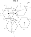
- FIG. 3 is the plan view schematically showing the columnar portions 30a, 30b, 30c, 30d.
- a line L1 is an imaginary line passing through the center Ca of the columnar portion 30a and the center Cb of the columnar portion 30b.
- the line L1 extends in a first direction.
- the line L1 is inclined relative to m-planes 31a, 31b located between the centers Ca, Cb.
- the m-plane 31a is a face of the columnar portion 30a.
- the m-plane 31b is a face of the columnar portion 30b.
- the columnar portion 30 has the six m-planes.
- the m-planes are side surfaces of the columnar portion 30.
- the line L1 is not orthogonal to the m-planes of all columnar portions 30 and not parallel to the m-planes of all columnar portions 30.
- the line L1 is inclined e.g. at from 8 degrees to 22 degrees relative to a perpendicular Pa of the m-plane 31a and a perpendicular Pb of the m-plane 31b.
- An angle ⁇ of the line L1 relative to the perpendicular Pa and an angle ⁇ of the line L1 relative to the perpendicular Pb are the same angle and the angle ⁇ is from 8 degrees to 22 degrees.
- vertices of the columnar portions 30a, 30b are not placed on the line L1. That is, the line L1 does not pass through the vertices of the columnar portions 30a, 30b. In the example shown in FIG. 2 , the line L1 does not pass through the vertices of all columnar portions 30.
- the vertices of the columnar portions 30 are connecting points of the m-planes.
- a line L2 is an imaginary line passing through the center Ca of the columnar portion 30a and the center Cc of the columnar portion 30c.
- the line L2 extends in a second direction orthogonal to the first direction and orthogonal to the line L1.
- the line L2 is inclined relative to m-planes 32a, 32c located between the centers Ca, Cc.
- the m-plane 32a is a face of the columnar portion 30a.
- the m-plane 32a is not connected to the m-plane 31a.
- the m-plane 32a is inclined at e.g. 60 degrees relative to the m-plane 31a.
- the m-plane 32c is a face of the columnar portion 30c.
- the m-plane 32a and the m-plane 32c are parallel.
- the line L2 is not orthogonal to the m-planes of all columnar portions 30 and not parallel to the m-planes of all columnar portions 30.
- the line L2 is inclined e.g. at from 8 degrees to 22 degrees relative to a perpendicular Qa of the m-plane 32a and a perpendicular Qc of the m-plane 32c.
- An angle ⁇ of the line L2 relative to the perpendicular Qa and an angle ⁇ of the line L2 relative to the perpendicular Qc are the same angle and the angle ⁇ is from 8 degrees to 22 degrees.
- the light emitting device 100 has the following characteristics.
- the multilaminated structure 12 has the plurality of columnar portions 30, the columnar portion 30 contains the material having the wurtzite-type crystal structure, in the plan view as seen from the laminated direction, the plurality of columnar portions 30 are arranged in the square lattice form, the line L1 passing through the centers Ca, Cb of the adjacent columnar portions 30a, 30b is inclined relative to the m-planes 31a, 31b of the columnar portions 30a, 30b located between the centers Ca, Cb of the adjacent columnar portions 30a, 30b, and the vertices of the adjacent columnar portions 30a, 30b are not placed on the line L1.
- the light emitting device 100 during the growth of the columnar portions 30, even when the columnar portions 30 grow in the lateral directions, i.e., the in-plane directions of the substrate 10, contact between the adjacent columnar portions 30a, 30b may be suppressed. If the adjacent columnar portions contact, power efficiency and the maximum optical output at light emission may be significantly reduced. Further, light at a desired wavelength is not emitted.
- the m-plane of the columnar portion 30 is a stable surface and, when the m-plane is formed when the columnar portion 30 grows, the columnar portion 30 is hard to grow from the m-plane in the lateral directions. Accordingly, when the columnar portion 30 grows in the lateral directions, as shown by arrows in FIG. 3 , the columnar portion 30 grows from the vertex as the connecting point between the m-planes in a direction connecting the center of the columnar portion and the vertex.
- the line L1 is inclined relative to the m-planes 31a, 31b and the vertices of the adjacent columnar portions 30a, 30b are not placed on the line L1, and thereby, an arrow A1 passing through the center Ca and the vertex at the end of the m-plane 31a and an arrow A2 passing through the center Cb and the vertex at the end of the m-plane 31b may be prevented from being in contact. Accordingly, in the light emitting device 100, as shown in FIG.
- the contact between the adjacent columnar portions 30a, 30b may be suppressed.
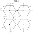
- the arrow A1 and the arrow A2 are in contact, for example, the distance between the center Ca and the connecting point between the arrow A1 and the arrow A2 may be made larger. Therefore, compared to the example shown in FIG. 4 , the contact between the adjacent columnar portions 30a, 30b may be suppressed.
- the distance between the centers Ca, Cb shown in FIG. 4 is the same as the distance between the centers Ca, Cb shown in FIG. 3 . Further, the distance between the centers Ca, Cc shown in FIG. 4 is the same as the distance between the centers Ca, Cc shown in FIG.3 .
- the line L2 passing through the centers Ca, Cc of the adjacent columnar portions 30a, 30c is inclined relative to the m-planes 32a, 32c of the columnar portions 30a, 30c located between the centers Ca, Cc of the adjacent columnar portions 30a, 30c, and the vertices of the adjacent columnar portions 30a, 30c are not placed on the line L2, and thereby, the contact between the adjacent columnar portions 30a, 30c may be suppressed.
- the line L1 is inclined at from 8 degrees to 22 degrees relative to the perpendiculars Pa, Pb of the m-planes 31a, 31b. Accordingly, in the light emitting device 100, the contact between the adjacent columnar portions 30a, 30b may be suppressed more reliably.
- the InGaN-based light emitting layer 36 is explained, however, the light emitting layer 36 may be an AlGaN-based layer.
- the light emitting device 100 is a laser
- the light emitting device 100 may be an LED.
- the columnar portion 30 does not necessarily have the light emitting layer 36.
- a structure is provided between the plurality of columnar portions 30 and the second electrode 52, and the structure may have the first semiconductor layer 34, the second semiconductor layer 38, and the light emitting layer 36 provided between the first semiconductor layer 34 and the second semiconductor layer 38.
- the columnar portion 30 may be formed by an n-type semiconductor layer.
- FIG. 6 is the flowchart for explanation of the method of manufacturing the light emitting device 100 according to the first embodiment.
- FIG. 7 is the sectional view schematically showing the manufacturing process of the light emitting device 100 according to the first embodiment.
- the substrate 10 is prepared (step S1).
- the multilaminated structure 12 having the plurality of columnar portions 30 is formed on the substrate 10 (step S2).
- the buffer layer 20 is epitaxially grown.
- the epitaxial growth method includes e.g. the MOCVD method and MBE method.
- the mask layer 22 is formed.
- the mask layer 22 is formed by e.g. the sputtering method.
- the mask layer 22 is patterned and the opening portions 23 are formed.
- the patterning is performed by e.g. photolithography and etching.
- the first semiconductor layers 34, the light emitting layers 36, and the second semiconductor layers 38 are epitaxially grown in this order on the buffer layer 20.
- the epitaxial growth method includes e.g. the MOCVD method and MBE method.
- the plurality of columnar portions 30 are arranged in the square lattice form. Further, the line L1 passing through the centers of the adjacent columnar portions 30a, 30b is inclined relative to the m-planes 31a, 31b of the columnar portions 30a, 30b located between the centers Ca, Cb of the adjacent columnar portions 30a, 30b. Furthermore, the vertices of the adjacent columnar portions 30a, 30b are not placed on the line L1. Moreover, the line L1 is inclined at e.g. from 8 degrees to 22 degrees relative to the perpendiculars Pa, Pb of the m-planes 31a, 31b.
- the orientation flat is set in a predetermined position, then, the wafer is rotated, the columnar portions 30 are grown from the opening portions 23 of the rotated wafer, and thereby, the angle ⁇ may be set from 8 degrees to 22 degrees. Or, the angle ⁇ may be set from 8 degrees to 22 degrees by adjustment of the mask for formation of the opening portions 23.
- the light propagation layer 40 is formed between the adjacent columnar portions 30.
- the light propagation layer 40 is formed by e.g. the spin-coating method.
- the multilaminated structure 12 may be formed.
- the first electrode 50 is formed on the buffer layer 20 and the second electrode 52 is formed on the second semiconductor layer 38 (step S3).
- the first electrode 50 and the second electrode 52 are formed by e.g. the vacuum deposition method.
- the light emitting device 100 may be manufactured.
- the method of manufacturing the light emitting device 100 may suppress the contact between the adjacent columnar portions 30a, 30b.
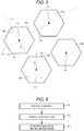
- the plurality of columnar portions 30 are arranged in the square lattice form, however, the plurality of columnar portions 30 may be arranged in a rectangular lattice form as shown in FIG. 8 . That is, of the plurality of columnar portions 30, the figure F formed by the line connecting the center Ca of the columnar portion 30a and the center Cb of the columnar portion 30b, the line connecting the center Ca of the columnar portion 30a and the center Cc of the columnar portion 30c, the line connecting the center Cb of the columnar portion 30b and the center Cd of the columnar portion 30d, and the line connecting the center Cc of the columnar portion 30c and the center Cd of the columnar portion 30d may be a rectangle.
- the distance between the center Ca of the columnar portion 30a and the center Cb of the columnar portion 30b is smaller than the distance between the center Ca of the columnar portion 30a and the center Cc of the columnar portion 30c. Even in this case, during the growth of the columnar portions 30, even when the columnar portions 30 grow in the lateral directions, the contact between the adjacent columnar portions 30a, 30b may be suppressed.
- FIG. 9 is the plan view schematically showing the light emitting device 200 according to the second embodiment. Note that, for convenience, in FIG. 9 , illustration of the other members than the columnar portions 30 is omitted.
- the differences from the example of the light emitting device 100 according to the above described first embodiment will be explained and the explanation of the same items will be omitted.
- the plurality of columnar portions 30 are arranged in the square lattice form in the plan view as seen from the laminated direction.
- the plurality of columnar portions 30 are arranged in a regular triangular lattice form in the plan view as seen from the laminated direction. That is, of the plurality of columnar portions 30, a figure F formed by a line connecting a center Ca of a columnar portion 30a and a center Cb of a columnar portion 30b, a line connecting the center Cb of the columnar portion 30b and a center Cc of a columnar portion 30c, and a line connecting the center Ca of the columnar portion 30a and the center Cc of the columnar portion 30c is a regular triangle.
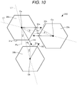
- FIG. 10 is the plan view schematically showing the columnar portions 30a, 30b, 30c.
- the line L1 and the line L2 cross at 60 degrees.
- the m-planes 31a, 32a of the columnar portion 30a are connected to each other.
- the plurality of columnar portions 30 are arranged in the regular triangular lattice form, and the line L1 passing through the centers Ca, Cb of the adjacent columnar portions 30a, 30b is inclined relative to the m-planes 31a, 31b of the columnar portions 30a, 30b located between the centers Ca, Cb of the adjacent columnar portions 30a, 30b, and the vertices of the adjacent columnar portions 30a, 30b are not placed on the line L1. Accordingly, in the light emitting device 200, compared to a case where the line L1 is orthogonal to the m-planes 31a, 31b as shown in FIG. 11 or a case where the line L1 passes through the vertices as shown in FIG. 12 , during the growth of the columnar portions 30, contact between the adjacent columnar portions 30a, 30b may be suppressed like the light emitting device 100.
- the distance between the centers Ca, Cb shown in FIG. 10 is the same as the distance between the centers Ca, Cb shown in FIGS. 11 and 12 . Further, the distance between the centers Ca, Cc shown in FIG. 10 is the same as the distance between the centers Ca, Cc shown in FIGS. 11 and 12 .
- the method of manufacturing the light emitting device 200 according to the second embodiment is basically the same as the method of manufacturing the light emitting device 100 according to the above described first embodiment except that the plurality of columnar portions 30 are arranged in the regular triangular lattice form. Accordingly, the detailed explanation thereof will be omitted.
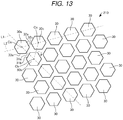
- FIGS. 13 and 14 are plan views schematically showing the light emitting device 210 according to the modified example of the second embodiment. Note that, for convenience, in FIG. 13 , illustration of the other members than the columnar portions 30 is omitted. Further, in FIG. 14 , illustration of the other members than the columnar portions 30a, 30b, 30c is omitted.
- the differences from the example of the light emitting device 200 according to the above described second embodiment will be explained and the explanation of the same items will be omitted.
- the light emitting device 210 is different from the above described light emitting device 200 in that the line L1 is inclined relative to a perpendicular Ra of the m-plane 33a of the columnar portion 30a at from 38 degrees to 52 degrees in the plan view as seen from the laminated direction. That is, an angle ⁇ of the line L1 relative to the perpendicular Ra is from 38 degrees to 52 degrees.
- the m-plane 33a is an m-plane connected to the m-plane 31a in a clockwise direction.
- a method of manufacturing the light emitting device 210 is basically the same as the above described method of manufacturing the light emitting device 200 except that the line L1 is inclined relative to the perpendicular Ra of the m-plane 33a at from 38 degrees to 52 degrees.
- the line L1 is inclined relative to the perpendicular Ra of the m-plane 33a connected to the m-plane 31a in the clockwise direction at from 38 degrees to 52 degrees. Accordingly, in the light emitting device 210, contact between the adjacent columnar portions 30a, 30b may be suppressed more realiably.
- FIG. 15 schematically shows the projector 900 according to the third embodiment.
- the projector 900 has the light emitting devices 100 as e.g. light sources.
- the projector 900 has a housing (not shown) and a red light source 100R, a green light source 100G, and a blue light source 100B provided within the housing and outputting a red light, a green light, and a blue light, respectively. Note that, for convenience, in FIG. 15 , the red light source 100R, the green light source 100G, and the blue light source 100B are simplified.
- the projector 900 further has a first lens array 902R, a second lens array 902G, a third lens array 902B, a first light modulation device 904R, a second light modulation device 904G, a third light modulation device 904B, and a projection device 908 provided within the housing.
- the first light modulation device 904R, the second light modulation device 904G, and the third light modulation device 904B are e.g. transmissive liquid crystal light valves.
- the projection device 908 is e.g. a projection lens.
- the light output from the red light source 100R enters the first lens array 902R.
- the light output from the red light source 100R is collected and may be superimposed, for example, by the first lens array 902R.
- the light collected by the first lens array 902R enters the first light modulation device 904R.
- the first light modulation device 904R modulates the entering light according to image information.
- the projection device 908 enlarges and projects an image formed by the first light modulation device 904R on a screen 910.
- the light output from the green light source 100G enters the second lens array 902G.
- the light output from the green light source 100G is collected and may be superimposed, for example, by the second lens array 902G.
- the light collected by the second lens array 902G enters the second light modulation device 904G.
- the second light modulation device 904G modulates the entering light according to the image information.
- the projection device 908 enlarges and projects an image formed by the second light modulation device 904G on the screen 910.
- the light output from the blue light source 100B enters the third lens array 902B.
- the light output from the blue light source 100B is collected and may be superimposed, for example, by the third lens array 902B.
- the light collected by the third lens array 902B enters the third light modulation device 904B.
- the third light modulation device 904B modulates the entering light according to the image information.
- the projection device 908 enlarges and projects an image formed by the third light modulation device 904B on the screen 910.
- the projector 900 may have a cross dichroic prism 906 that combines and guides the lights output from the first light modulation device 904R, the second light modulation device 904G, and the third light modulation device 904B to the projection device 908.
- the cross dichroic prism 906 is formed by bonding of four rectangular prisms, and a dielectric multilayer film that reflects the red light and a dielectric multilayer film that reflects the blue light are placed on the inner surfaces thereof.
- the three color lights are combined by these dielectric multilayer films and a light representing a color image is formed.
- the combined light is projected by the projection device 908 on the screen 910 and the enlarged image is displayed.
- the red light source 100R, the green light source 100G, and the blue light source 100B may control the light emitting devices 100 as pixels of pictures according to the image information, and thereby, directly form the pictures without using the first light modulation device 904R, the second light modulation device 904G, and the third light modulation device 904B. Further, the projection device 908 may enlarge and project the pictures formed by the red light source 100R, the green light source 100G, and the blue light source 100B on the screen 910.
- the transmissive liquid crystal light valves are used as the light modulation devices, however, light valves of other types than liquid crystal may be used or reflective light valves may be used.
- the light valves include e.g. reflective liquid crystal light valves and digital micro mirror devices.
- the configuration of the projection device is appropriately changed according to the type of the light valves in use.
- the light source can be applied to a light source device of a scanning image display apparatus having a scanning unit in which an image having a desired size is displayed on a display surface by scanning with lights from the light source on a screen.
- the application of the light emitting device according to the present disclosure is not limited to the above described embodiments, but the device may be used for other apparatuses than the projector.
- the application to other apparatuses than the projector includes light sources for e.g. illuminations indoor or outdoor, back lights for display, laser printers, scanners, on-vehicle lights, sensing devices using lights, communication devices, etc.
- an n-type GaN was grown as a buffer layer by the MOCVD method. Then, a mask layer was formed on the buffer layer by the sputtering method, and opening portions having circular planar shapes were formed in the mask layer by patterning. Then, using the mask layer as a mask, an n-type GaN was formed and a plurality of columnar portions were formed. In the above described sample, the arrangement of the columnar portions was varied.
- Practical example 1 corresponds to the light emitting device shown in FIGS. 2 and 3 in which the plurality of columnar portions are arranged in the square lattice form and ⁇ is 8 degrees.
- Practical example 2 corresponds to the light emitting device shown in FIGS. 9 and 10 in which the plurality of columnar portions are arranged in the regular triangular lattice form and ⁇ is 8 degrees.
- Practical example 3 corresponds to the light emitting device shown in FIGS. 13 and 14 in which the plurality of columnar portions are arranged in the regular triangular lattice form and ⁇ is 38 degrees.
- Comparative example 1 corresponds to the light emitting device shown in FIG. 4 in which the plurality of columnar portions are arranged in the square lattice form and the L1 is orthogonal to the m-planes.
- Comparative example 2 corresponds to the light emitting device shown in FIG. 11 in which the plurality of columnar portions are arranged in the regular triangular lattice form and the L1 is orthogonal to the m-planes.
- Comparative example 3 corresponds to the light emitting device shown in FIG. 12 in which the plurality of columnar portions are arranged in the regular triangular lattice form and the L1 passes through the vertices.
- FIG. 16 is the SEM image of practical example 1.
- FIG. 17 is the SEM image of practical example 2.
- FIG. 18 is the SEM image of practical example 3.
- FIG. 19 is the SEM image of comparative example 1.
- FIG. 20 is the SEM image of comparative example 2.
- FIG. 21 is the SEM image of comparative example 3.
- the present disclosure may be embodied by omission of a part of the configuration or combination of the respective embodiments and modified examples within a range in which the characteristics and the effects described in this application are provided.
- the present disclosure is not limited to the above described embodiments, but other various modifications can be made.
- the present disclosure includes substantially the same configurations as the configurations described in the embodiments. "Substantially the same configurations" are e.g. the configurations having the same functions, methods, and results or the configurations having the same purposes and effects.
- the present disclosure includes configurations in which inessential parts of the configurations described in the embodiments are replaced.
- the present disclosure includes configurations that exert the same effects or configurations that may achieve the same purposes as those of the configurations described in the embodiments.
- the present disclosure includes configurations with the addition of known techniques to the configurations described in the embodiments.
Landscapes
- Physics & Mathematics (AREA)
- General Physics & Mathematics (AREA)
- Optics & Photonics (AREA)
- Condensed Matter Physics & Semiconductors (AREA)
- Electromagnetism (AREA)
- Geometry (AREA)
- Led Devices (AREA)
- Projection Apparatus (AREA)
- Transforming Electric Information Into Light Information (AREA)
- Semiconductor Lasers (AREA)
- Non-Portable Lighting Devices Or Systems Thereof (AREA)
Abstract
Description
- The present application is based on, and claims priority from
JP Application Serial Number 2019-069998, filed April 1, 2019 - The present disclosure relates to a light emitting device, a method of manufacturing the light emitting device, and a projector.
- These days, development of small projectors including nanocolumns as light sources are advanced. The small projectors may have light sources with higher efficiency, higher intensity, and longer lives than LED (Light Emitting Diode) light sources of related art, and attract attention as environment-friendly energy-saving projectors.
- For example,
JP-A-2013-239718 - However, during the growth of columnar portions, the columnar portions may grow in lateral directions and the adjacent columnar portions may contact.
- An aspect of a light emitting device according to the present disclosure includes a substrate, and a laminated structure provided on the substrate, wherein the laminated structure has a plurality of columnar portions, the columnar portion contains a material having a wurtzite-type crystal structure, in a plan view as seen from a laminated direction of the laminated structure, the plurality of columnar portions are arranged in a square lattice form or rectangular lattice form, a line passing through centers of the adjacent columnar portions is inclined relative to m-planes of the columnar portions located between the centers of the adjacent columnar portions, and vertices of the adjacent columnar portions are not placed on the line.
- In the aspect of the light emitting device, in the plan view as seen from the laminated direction, the line may be inclined at from 8 degrees to 22 degrees relative to perpendiculars of the m-planes.
- An aspect of a light emitting device according to the present disclosure includes a substrate, and a laminated structure provided on the substrate, wherein the laminated structure has a plurality of columnar portions, the columnar portion contains a material having a wurtzite-type crystal structure, in a plan view as seen from a laminated direction of the laminated structure, the plurality of columnar portions are arranged in a regular triangular lattice form, a line passing through centers of the adjacent columnar portions is inclined relative to m-planes of the columnar portions located between the centers of the adjacent columnar portions, and vertices of the adjacent columnar portions are not placed on the line.
- In the aspect of the light emitting device, in the plan view as seen from the laminated direction, the line may be inclined at from 8 degrees to 22 degrees relative to perpendiculars of the m-planes.
- In the aspect of the light emitting device, in the plan view as seen from the laminated direction, the line may be inclined at from 38 degrees to 52 degrees relative to a perpendicular of an m-plane connected to the m-plane in a clockwise direction.
- An aspect of a method of manufacturing a light emitting device according to the present disclosure includes forming a laminated structure having a plurality of columnar portions on a substrate, wherein the columnar portion contains a material having a wurtzite-type crystal structure, at forming the laminated structure, in a plan view as seen from a laminated direction of the laminated structure, the plurality of columnar portions are arranged in a square lattice form or rectangular lattice form, a line passing through centers of the adjacent columnar portions is inclined relative to m-planes of the columnar portions located between the centers of the adjacent columnar portions, and vertices of the adjacent columnar portions are not placed on the line.
- In the aspect of the method of manufacturing a light emitting device, at forming the laminated structure, in the plan view as seen from the laminated direction, the line may be inclined at from 8 degrees to 22 degrees relative to perpendiculars of the m-planes.
- An aspect of a method of manufacturing a light emitting device according to the present disclosure includes forming a laminated structure having a plurality of columnar portions on a substrate, wherein the columnar portion contains a material having a wurtzite-type crystal structure, at forming the laminated structure, in a plan view as seen from a laminated direction of the laminated structure, the plurality of columnar portions are arranged in a regular triangular lattice form, a line passing through centers of the adjacent columnar portions is inclined relative to m-planes of the columnar portions located between the centers of the adjacent columnar portions, and vertices of the adjacent columnar portions are not placed on the line.
- In the aspect of the method of manufacturing a light emitting device, at forming the laminated structure, in the plan view as seen from the laminated direction, the line may be inclined at from 8 degrees to 22 degrees relative to perpendiculars of the m-planes.
- In the aspect of the method of manufacturing a light emitting device, at forming the laminated structure, in the plan view as seen from the laminated direction, the line may be inclined at from 38 degrees to 52 degrees relative to a perpendicular of an m-plane connected to the m-plane in a clockwise direction.
- An aspect of a projector according to the present disclosure includes the above described aspect of the light emitting device.
-
-
FIG. 1 is a sectional view schematically showing a light emitting device according to a first embodiment. -
FIG. 2 is a plan view schematically showing the light emitting device according to the first embodiment. -
FIG. 3 is a plan view schematically showing the light emitting device according to the first embodiment. -
FIG. 4 is a plan view schematically showing columnar portions arranged in a square lattice form. -
FIG. 5 is a plan view schematically showing columnar portions arranged in a square lattice form. -
FIG. 6 is a flowchart for explanation of a method of manufacturing the light emitting device according to the first embodiment. -
FIG. 7 is a sectional view schematically showing a manufacturing process of the light emitting device according to the first embodiment. -
FIG. 8 is a plan view schematically showing the light emitting device according to the first embodiment. -
FIG. 9 is a plan view schematically showing a light emitting device according to a second embodiment. -
FIG. 10 is a plan view schematically showing the light emitting device according to the second embodiment. -
FIG. 11 is a plan view schematically showing columnar portions arranged in a regular triangular lattice form. -
FIG. 12 is a plan view schematically showing columnar portions arranged in a regular triangular lattice form. -
FIG. 13 is a plan view schematically showing a light emitting device according to a modified example of the second embodiment. -
FIG. 14 is a plan view schematically showing the light emitting device according to the modified example of the second embodiment. -
FIG. 15 schematically shows a projector according to a third embodiment. -
FIG. 16 is a SEM image of practical example 1. -
FIG. 17 is a SEM image of practical example 2. -
FIG. 18 is a SEM image of practical example 3. -
FIG. 19 is a SEM image of comparative example 1. -
FIG. 20 is a SEM image of comparative example 2. -
FIG. 21 is a SEM image of comparative example 3. - As below, preferred embodiments of the present disclosure will be explained using the drawings. Note that the following embodiments do not unduly limit the present disclosure described in the appended claims. Not all of the configurations to be explained are essential component elements of the present disclosure.
- First, a light emitting device according to the first embodiment will be explained with reference to the drawings.
FIG. 1 is the sectional view schematically showing thelight emitting device 100 according to the first embodiment.FIG. 2 is the plan view schematically showing thelight emitting device 100 according to the first embodiment.FIG. 1 is the sectional view along line I-I inFIG. 2 . - As shown in
FIG. 1 , thelight emitting device 100 has e.g. asubstrate 10, amultilaminated structure 12 provided on thesubstrate 10, afirst electrode 50, and asecond electrode 52. Themultilaminated structure 12 has abuffer layer 20, amask layer 22,columnar portions 30, and alight propagation layer 40. For convenience, inFIG. 2 , illustration of the other members than thecolumnar portions 30 is omitted. - The
substrate 10 is e.g. a sapphire substrate, GaN substrate, Si substrate, or the like. - The
buffer layer 20 is provided on thesubstrate 10. Thebuffer layer 20 is e.g. a Si-doped n-type GaN layer or the like. - Note that "upper" refers to a direction away from the
substrate 10 as seen from a light emitting layer 36 in a laminated direction of the multilaminated structure 12 (hereinafter, also simply referred to as "laminated direction"), and "lower" refers to a direction toward thesubstrate 10 as seen from the light emitting layer 36 in the laminated direction. The laminated direction of the laminatedstructure 12 is a laminated direction of afirst semiconductor layer 34 and the light emitting layer 36 of thecolumnar portion 30. Hereinafter, a direction orthogonal to the laminated direction is also referred to as "in-plane direction of thesubstrate 10". - The
mask layer 22 is provided on thebuffer layer 20. A plurality of openingportions 23 are provided in themask layer 22. As seen from the laminated direction, the shape of the openingportion 23 is e.g. a circular shape. Thecolumnar portion 30 is provided in the openingportion 23. Themask layer 22 is a layer that functions as a mask for growing thecolumnar portions 30. The material of themask layer 22 is e.g. an SiO2 layer, Si layer, SiC layer, TiO2 layer, HfO2 layer, or the like. - The
columnar portions 30 are provided on thebuffer layer 20. Thecolumnar portion 30 is formed using a GaN-based material containing gallium (Ga) and nitrogen (N). The GaN-based material has a wurtzite-type crystal structure, and thecolumnar portion 30 tends to grow in a planar shape of regular hexagon. In the example shown inFIG. 2 , the planar shape of thecolumnar portion 30 is a regular hexagonal shape. For example, the diameter of thecolumnar portion 30 is on the order of nanometers, and specifically from 50 nm to 500 nm. The size of thecolumnar portion 30 in the laminated direction is e.g. from 0.5 µm to 3 µm . The material having the wurtzite-type crystal structure includes e.g. an AlN-based material, ZnO-based material, ZnS-based material, and InN-based material in addition to the GaN-based material. - Note that "diameter" is a diameter of the smallest circle internally containing the
columnar portion 30 having a polygonal planar shape, i.e., the smallest enclosing circle. Further, "planar shape" refers to a shape as seen from the laminated direction. The center of thecolumnar portion 30 is the center of the smallest enclosing circle. - A plurality of the
columnar portions 30 are provided. Thecolumnar portions 30 are periodically arranged in predetermined directions in predetermined pitches. The pitch of thecolumnar portions 30 is e.g. from 200 nm to 1 µm. Here, "pitch" refers to a distance for single period when thecolumnar portions 30 are periodically arranged. In this case, the pitch is e.g. a distance between the centers of the adjacentcolumnar portions 30. - The
columnar portion 30 has thefirst semiconductor layer 34, the light emitting layer 36, and asecond semiconductor layer 38. - The
first semiconductor layer 34 is provided on thebuffer layer 20. Thefirst semiconductor layer 34 is e.g. a Si-doped n-type GaN layer. - The light emitting layer 36 is provided on the
first semiconductor layer 34. The light emitting layer 36 is provided between thefirst semiconductor layer 34 and thesecond semiconductor layer 38. The light emitting layer 36 has a quantum well structure formed by e.g. a GaN layer and an InGaN layer. The light emitting layer 36 is a layer that can emit light when a current is injected thereto. - The
second semiconductor layer 38 is provided on the light emitting layer 36. Thesecond semiconductor layer 38 is a layer having a different conductivity type from thefirst semiconductor layer 34. Thesecond semiconductor layer 38 is e.g. an Mg-doped p-type GaN layer. The semiconductor layers 34, 38 are cladding layers having functions of confining light in the light emitting layer 36. - In the
light emitting device 100, a pin diode is formed by the p-typesecond semiconductor layer 38, the light emitting layer 36 doped with no impurity, and the n-typefirst semiconductor layer 34. In thelight emitting device 100, when a forward bias voltage is applied and a current is injected between thefirst electrode 50 and thesecond electrode 52, electron-hole recombination occurs in the light emitting layer 36. Light is emitted by the recombination. The lights emitted in the light emitting layers 36 propagate through thelight propagation layer 40 in the in-plane directions of thesubstrate 10 by the semiconductor layers 34,38, form standing wave by the effect of photonic crystal by the plurality ofcolumnar portions 30, and are confined in the in-plane directions of thesubstrate 10. The confined lights laser-oscillate with gain in the light emitting layers 36. Then, thelight emitting device 100 outputs +1st-order diffracted light and -1st-order diffracted light as a laser beam in the laminated direction. - Note that a reflection layer (not shown) may be provided between the
substrate 10 and thebuffer layer 20 or under thesubstrate 10. The reflection layer is e.g. a DBR (Distributed Bragg Reflector) layer. By the reflection layer, the light generated in the light emitting layer 36 may be reflected, and thelight emitting device 100 may output light only from thesecond electrode 52 side. - The
light propagation layer 40 is provided between the adjacentcolumnar portions 30. In the illustrated example, thelight propagation layer 40 is provided on themask layer 22. For example, the refractive index of thelight propagation layer 40 is lower than the refractive index of the light emitting layer 36. Thelight propagation layer 40 is e.g. a silicon oxide layer, aluminum oxide layer, titanium oxide layer, or the like. The light generated in the light emitting layer 36 can propagate in thelight propagation layer 40. Here, "adjacentcolumnar portions 30" refers to a firstcolumnar portion 30 of the plurality ofcolumnar portions 30 and a secondcolumnar portion 30 at the shortest distance between centers to the firstcolumnar portion 30 of the plurality ofcolumnar portions 30. - The
first electrode 50 is provided on thebuffer layer 20. Thebuffer layer 20 may be in ohmic contact with thefirst electrode 50. In the illustrated example, thefirst electrode 50 is electrically coupled to thefirst semiconductor layer 34 via thebuffer layer 20. Thefirst electrode 50 is one electrode for current injection to the light emitting layer 36. As thefirst electrode 50, e.g. a laminated structure of a Ti layer, an Al layer, an Au layer sequentially from thebuffer layer 20 side or the like is used. - The
second electrode 52 is provided on thesecond semiconductor layer 38. Thesecond semiconductor layer 38 may be in ohmic contact with thesecond electrode 52. Thesecond electrode 52 is electrically coupled to thesecond semiconductor layer 38. Thesecond electrode 52 is the other electrode for current injection to the light emitting layer 36. The material of thesecond electrode 52 is e.g. ITO (Indium Tin Oxide) or the like. - As shown in
FIG. 2 , the plurality ofcolumnar portions 30 are arranged in a square lattice form in a plan view as seen from the laminated direction. That is, of the plurality ofcolumnar portions 30, a figure F formed by a line connecting a center Ca of acolumnar portion 30a and a center Cb of acolumnar portion 30b, a line connecting the center Ca of thecolumnar portion 30a and a center Cc of acolumnar portion 30c, a line connecting the center Cb of thecolumnar portion 30b and a center Cd of acolumnar portion 30d, and a line connecting the center Cc of thecolumnar portion 30c and the center Cd of thecolumnar portion 30d is a square. In the plan view as seen from the laminated direction, the position of the center of thecolumnar portion 30 coincides with the position of the center of the openingportion 23 provided in themask layer 22. - In the illustrated example, the
columnar portion 30b is adjacent to thecolumnar portion 30a, and thecolumnar portion 30c is adjacent to thecolumnar portion 30a. In the illustrated example, the twentycolumnar portions 30 are provided, however, the number ofcolumnar portion 30 is not particularly limited. - Here,
FIG. 3 is the plan view schematically showing thecolumnar portions FIGS. 2 and3 , in the plan view as seen from the laminated direction, a line L1 is an imaginary line passing through the center Ca of thecolumnar portion 30a and the center Cb of thecolumnar portion 30b. The line L1 extends in a first direction. - The line L1 is inclined relative to m-
planes plane 31a is a face of thecolumnar portion 30a. The m-plane 31b is a face of thecolumnar portion 30b. For example, the m-plane 31a and the m-plane 31b are parallel. Thecolumnar portion 30 has the six m-planes. The m-planes are side surfaces of thecolumnar portion 30. In the example shown inFIG. 2 , the line L1 is not orthogonal to the m-planes of allcolumnar portions 30 and not parallel to the m-planes of allcolumnar portions 30. - As shown in
FIG. 3 , the line L1 is inclined e.g. at from 8 degrees to 22 degrees relative to a perpendicular Pa of the m-plane 31a and a perpendicular Pb of the m-plane 31b. An angle θ of the line L1 relative to the perpendicular Pa and an angle θ of the line L1 relative to the perpendicular Pb are the same angle and the angle θ is from 8 degrees to 22 degrees. - In the plan view as seen from the laminated direction, vertices of the
columnar portions columnar portions FIG. 2 , the line L1 does not pass through the vertices of allcolumnar portions 30. The vertices of thecolumnar portions 30 are connecting points of the m-planes. - As shown in
FIGS. 2 and3 , in the plan view as seen from the laminated direction, a line L2 is an imaginary line passing through the center Ca of thecolumnar portion 30a and the center Cc of thecolumnar portion 30c. The line L2 extends in a second direction orthogonal to the first direction and orthogonal to the line L1. - The line L2 is inclined relative to m-
planes plane 32a is a face of thecolumnar portion 30a. The m-plane 32a is not connected to the m-plane 31a. The m-plane 32a is inclined at e.g. 60 degrees relative to the m-plane 31a. The m-plane 32c is a face of thecolumnar portion 30c. For example, the m-plane 32a and the m-plane 32c are parallel. In the example shown inFIG. 2 , the line L2 is not orthogonal to the m-planes of allcolumnar portions 30 and not parallel to the m-planes of allcolumnar portions 30. - As shown in
FIG. 3 , the line L2 is inclined e.g. at from 8 degrees to 22 degrees relative to a perpendicular Qa of the m-plane 32a and a perpendicular Qc of the m-plane 32c. An angle θ of the line L2 relative to the perpendicular Qa and an angle θ of the line L2 relative to the perpendicular Qc are the same angle and the angle θ is from 8 degrees to 22 degrees. - In the plan view as seen from the laminated direction, vertices of the
columnar portions columnar portions FIG. 2 , the line L2 does not pass through the vertices of allcolumnar portions 30. - For example, the
light emitting device 100 has the following characteristics. - In the
light emitting device 100, themultilaminated structure 12 has the plurality ofcolumnar portions 30, thecolumnar portion 30 contains the material having the wurtzite-type crystal structure, in the plan view as seen from the laminated direction, the plurality ofcolumnar portions 30 are arranged in the square lattice form, the line L1 passing through the centers Ca, Cb of the adjacentcolumnar portions planes columnar portions columnar portions columnar portions light emitting device 100, during the growth of thecolumnar portions 30, even when thecolumnar portions 30 grow in the lateral directions, i.e., the in-plane directions of thesubstrate 10, contact between the adjacentcolumnar portions - Here, the m-plane of the
columnar portion 30 is a stable surface and, when the m-plane is formed when thecolumnar portion 30 grows, thecolumnar portion 30 is hard to grow from the m-plane in the lateral directions. Accordingly, when thecolumnar portion 30 grows in the lateral directions, as shown by arrows inFIG. 3 , thecolumnar portion 30 grows from the vertex as the connecting point between the m-planes in a direction connecting the center of the columnar portion and the vertex. - As described above, in the
light emitting device 100, the line L1 is inclined relative to the m-planes columnar portions plane 31a and an arrow A2 passing through the center Cb and the vertex at the end of the m-plane 31b may be prevented from being in contact. Accordingly, in thelight emitting device 100, as shown inFIG. 4 , compared to a case where the line L1 is orthogonal to the m-planes columnar portions 30, even when thecolumnar portions 30 grow in the lateral directions, the contact between the adjacentcolumnar portions FIG. 4 , the contact between the adjacentcolumnar portions - Note that the distance between the centers Ca, Cb shown in
FIG. 4 is the same as the distance between the centers Ca, Cb shown inFIG. 3 . Further, the distance between the centers Ca, Cc shown inFIG. 4 is the same as the distance between the centers Ca, Cc shown inFIG.3 . - Similarly, in the
light emitting device 100, the line L2 passing through the centers Ca, Cc of the adjacentcolumnar portions planes columnar portions columnar portions columnar portions columnar portions - In the
light emitting device 100, in the plan view as seen from the laminated direction, the line L1 is inclined at from 8 degrees to 22 degrees relative to the perpendiculars Pa, Pb of the m-planes light emitting device 100, the contact between the adjacentcolumnar portions - Here, as shown in "4. Practical Examples and Comparative Examples", which will be described later, a contact prevention effect between the adjacent columnar portions was confirmed when θ is 8 degrees. On the other hand when θ is 30 degrees, as shown in
FIG. 5 , the line L1 passes through the vertices of thecolumnar portions FIG. 4 . Therefore, within the range 8° ≤ θ ≤ 22°, which is obtained by subtraction of 8 degrees from 30 degrees, the contact between the adjacentcolumnar portions - Note that, in the above description, the InGaN-based light emitting layer 36 is explained, however, the light emitting layer 36 may be an AlGaN-based layer.
- Further, in the above description, the case where the
light emitting device 100 is a laser is explained, however, thelight emitting device 100 may be an LED. - Furthermore, in the above description, the case where the
columnar portion 30 has the light emitting layer 36 is explained, however, thecolumnar portion 30 does not necessarily have the light emitting layer 36. For example, a structure is provided between the plurality ofcolumnar portions 30 and thesecond electrode 52, and the structure may have thefirst semiconductor layer 34, thesecond semiconductor layer 38, and the light emitting layer 36 provided between thefirst semiconductor layer 34 and thesecond semiconductor layer 38. In this case, thecolumnar portion 30 may be formed by an n-type semiconductor layer. - Next, a method of manufacturing the
light emitting device 100 according to the first embodiment will be explained with reference to the drawings.FIG. 6 is the flowchart for explanation of the method of manufacturing thelight emitting device 100 according to the first embodiment.FIG. 7 is the sectional view schematically showing the manufacturing process of thelight emitting device 100 according to the first embodiment. - As shown in
FIG. 7 , thesubstrate 10 is prepared (step S1). - Then, the
multilaminated structure 12 having the plurality ofcolumnar portions 30 is formed on the substrate 10 (step S2). - Specifically, the
buffer layer 20 is epitaxially grown. The epitaxial growth method includes e.g. the MOCVD method and MBE method. - Then, the
mask layer 22 is formed. Themask layer 22 is formed by e.g. the sputtering method. Then, themask layer 22 is patterned and the openingportions 23 are formed. The patterning is performed by e.g. photolithography and etching. - As shown in
FIG. 1 , with themask layer 22 as a mask, from the plurality of openingportions 23, the first semiconductor layers 34, the light emitting layers 36, and the second semiconductor layers 38 are epitaxially grown in this order on thebuffer layer 20. The epitaxial growth method includes e.g. the MOCVD method and MBE method. - In this process, in the plan view as seen from the laminated direction, the plurality of
columnar portions 30 are arranged in the square lattice form. Further, the line L1 passing through the centers of the adjacentcolumnar portions planes columnar portions columnar portions columnar portions planes substrate 10, the orientation flat is set in a predetermined position, then, the wafer is rotated, thecolumnar portions 30 are grown from the openingportions 23 of the rotated wafer, and thereby, the angle θ may be set from 8 degrees to 22 degrees. Or, the angle θ may be set from 8 degrees to 22 degrees by adjustment of the mask for formation of the openingportions 23. - Then, the
light propagation layer 40 is formed between the adjacentcolumnar portions 30. Thelight propagation layer 40 is formed by e.g. the spin-coating method. - In the above described process, the
multilaminated structure 12 may be formed. - Then, the
first electrode 50 is formed on thebuffer layer 20 and thesecond electrode 52 is formed on the second semiconductor layer 38 (step S3). Thefirst electrode 50 and thesecond electrode 52 are formed by e.g. the vacuum deposition method. - In the above described process, the
light emitting device 100 may be manufactured. - As explained in "1.1.3. Characteristics", during the growth of the
columnar portions 30, even when thecolumnar portions 30 grow in the lateral directions, the method of manufacturing thelight emitting device 100 may suppress the contact between the adjacentcolumnar portions - Note that, in the above description, the plurality of
columnar portions 30 are arranged in the square lattice form, however, the plurality ofcolumnar portions 30 may be arranged in a rectangular lattice form as shown inFIG. 8 . That is, of the plurality ofcolumnar portions 30, the figure F formed by the line connecting the center Ca of thecolumnar portion 30a and the center Cb of thecolumnar portion 30b, the line connecting the center Ca of thecolumnar portion 30a and the center Cc of thecolumnar portion 30c, the line connecting the center Cb of thecolumnar portion 30b and the center Cd of thecolumnar portion 30d, and the line connecting the center Cc of thecolumnar portion 30c and the center Cd of thecolumnar portion 30d may be a rectangle. In the illustrated example, the distance between the center Ca of thecolumnar portion 30a and the center Cb of thecolumnar portion 30b is smaller than the distance between the center Ca of thecolumnar portion 30a and the center Cc of thecolumnar portion 30c. Even in this case, during the growth of thecolumnar portions 30, even when thecolumnar portions 30 grow in the lateral directions, the contact between the adjacentcolumnar portions - Next, a light emitting device according to the second embodiment will be explained with reference to the drawings.
FIG. 9 is the plan view schematically showing thelight emitting device 200 according to the second embodiment. Note that, for convenience, inFIG. 9 , illustration of the other members than thecolumnar portions 30 is omitted. - As below, in the
light emitting device 200 according to the second embodiment, the differences from the example of thelight emitting device 100 according to the above described first embodiment will be explained and the explanation of the same items will be omitted. - In the above described light
emitting device 100, as shown inFIG. 2 , the plurality ofcolumnar portions 30 are arranged in the square lattice form in the plan view as seen from the laminated direction. - On the other hand, in the
light emitting device 200, as shown inFIG. 9 , the plurality ofcolumnar portions 30 are arranged in a regular triangular lattice form in the plan view as seen from the laminated direction. That is, of the plurality ofcolumnar portions 30, a figure F formed by a line connecting a center Ca of acolumnar portion 30a and a center Cb of acolumnar portion 30b, a line connecting the center Cb of thecolumnar portion 30b and a center Cc of acolumnar portion 30c, and a line connecting the center Ca of thecolumnar portion 30a and the center Cc of thecolumnar portion 30c is a regular triangle. - Here,
FIG. 10 is the plan view schematically showing thecolumnar portions FIGS. 9 and10 , in the plan view as seen from the laminated direction, the line L1 and the line L2 cross at 60 degrees. The m-planes columnar portion 30a are connected to each other. - In the
light emitting device 200, in the plan view as seen from the laminated direction, the plurality ofcolumnar portions 30 are arranged in the regular triangular lattice form, and the line L1 passing through the centers Ca, Cb of the adjacentcolumnar portions planes columnar portions columnar portions columnar portions light emitting device 200, compared to a case where the line L1 is orthogonal to the m-planes FIG. 11 or a case where the line L1 passes through the vertices as shown inFIG. 12 , during the growth of thecolumnar portions 30, contact between the adjacentcolumnar portions light emitting device 100. - Note that the distance between the centers Ca, Cb shown in
FIG. 10 is the same as the distance between the centers Ca, Cb shown inFIGS. 11 and12 . Further, the distance between the centers Ca, Cc shown inFIG. 10 is the same as the distance between the centers Ca, Cc shown inFIGS. 11 and12 . - Next, a method of manufacturing the
light emitting device 200 according to the second embodiment will be explained. The method of manufacturing thelight emitting device 200 according to the second embodiment is basically the same as the method of manufacturing thelight emitting device 100 according to the above described first embodiment except that the plurality ofcolumnar portions 30 are arranged in the regular triangular lattice form. Accordingly, the detailed explanation thereof will be omitted. - Next, a light emitting device according to a modified example of the second embodiment will be explained with reference to the drawings.
FIGS. 13 and14 are plan views schematically showing thelight emitting device 210 according to the modified example of the second embodiment. Note that, for convenience, inFIG. 13 , illustration of the other members than thecolumnar portions 30 is omitted. Further, inFIG. 14 , illustration of the other members than thecolumnar portions - As below, in the
light emitting device 210 according to the modified example of the second embodiment, the differences from the example of thelight emitting device 200 according to the above described second embodiment will be explained and the explanation of the same items will be omitted. - As shown in
FIGS. 13 and14 , thelight emitting device 210 is different from the above described lightemitting device 200 in that the line L1 is inclined relative to a perpendicular Ra of the m-plane 33a of thecolumnar portion 30a at from 38 degrees to 52 degrees in the plan view as seen from the laminated direction. That is, an angle φ of the line L1 relative to the perpendicular Ra is from 38 degrees to 52 degrees. In the plan view as seen from the laminated direction, the m-plane 33a is an m-plane connected to the m-plane 31a in a clockwise direction. - A method of manufacturing the
light emitting device 210 is basically the same as the above described method of manufacturing thelight emitting device 200 except that the line L1 is inclined relative to the perpendicular Ra of the m-plane 33a at from 38 degrees to 52 degrees. - In the
light emitting device 210, in the plan view as seen from the laminated direction, the line L1 is inclined relative to the perpendicular Ra of the m-plane 33a connected to the m-plane 31a in the clockwise direction at from 38 degrees to 52 degrees. Accordingly, in thelight emitting device 210, contact between the adjacentcolumnar portions - Here, as shown in "4. Practical Examples and Comparative Examples", which will be described later, a contact prevention effect between the adjacent columnar portions was confirmed when φ is 38 degrees. On the other hand, when Φ is 60 degrees, the line L1 is orthogonal to the m-plane and is substantially the same as that in the example shown in
FIG. 11 . Therefore, within therange 38° ≤ φ ≤ 52°, which is obtained by subtraction of 8 degrees from 60 degrees, the contact between the adjacentcolumnar portions - Next, a projector according to the third embodiment will be explained with reference to the drawings.
FIG. 15 schematically shows theprojector 900 according to the third embodiment. - The
projector 900 has thelight emitting devices 100 as e.g. light sources. - The
projector 900 has a housing (not shown) and ared light source 100R, agreen light source 100G, and a bluelight source 100B provided within the housing and outputting a red light, a green light, and a blue light, respectively. Note that, for convenience, inFIG. 15 , thered light source 100R, thegreen light source 100G, and the bluelight source 100B are simplified. - The
projector 900 further has afirst lens array 902R, asecond lens array 902G, athird lens array 902B, a firstlight modulation device 904R, a secondlight modulation device 904G, a thirdlight modulation device 904B, and aprojection device 908 provided within the housing. The firstlight modulation device 904R, the secondlight modulation device 904G, and the thirdlight modulation device 904B are e.g. transmissive liquid crystal light valves. Theprojection device 908 is e.g. a projection lens. - The light output from the
red light source 100R enters thefirst lens array 902R. The light output from thered light source 100R is collected and may be superimposed, for example, by thefirst lens array 902R. - The light collected by the
first lens array 902R enters the firstlight modulation device 904R. The firstlight modulation device 904R modulates the entering light according to image information. Then, theprojection device 908 enlarges and projects an image formed by the firstlight modulation device 904R on ascreen 910. - The light output from the
green light source 100G enters thesecond lens array 902G. The light output from thegreen light source 100G is collected and may be superimposed, for example, by thesecond lens array 902G. - The light collected by the
second lens array 902G enters the secondlight modulation device 904G. The secondlight modulation device 904G modulates the entering light according to the image information. Then, theprojection device 908 enlarges and projects an image formed by the secondlight modulation device 904G on thescreen 910. - The light output from the blue
light source 100B enters thethird lens array 902B. The light output from the bluelight source 100B is collected and may be superimposed, for example, by thethird lens array 902B. - The light collected by the
third lens array 902B enters the thirdlight modulation device 904B. The thirdlight modulation device 904B modulates the entering light according to the image information. Then, theprojection device 908 enlarges and projects an image formed by the thirdlight modulation device 904B on thescreen 910. - Further, the
projector 900 may have a crossdichroic prism 906 that combines and guides the lights output from the firstlight modulation device 904R, the secondlight modulation device 904G, and the thirdlight modulation device 904B to theprojection device 908. - The three color lights modulated by the first
light modulation device 904R, the secondlight modulation device 904G, and the thirdlight modulation device 904B enter the crossdichroic prism 906. The crossdichroic prism 906 is formed by bonding of four rectangular prisms, and a dielectric multilayer film that reflects the red light and a dielectric multilayer film that reflects the blue light are placed on the inner surfaces thereof. The three color lights are combined by these dielectric multilayer films and a light representing a color image is formed. The combined light is projected by theprojection device 908 on thescreen 910 and the enlarged image is displayed. - Note that the
red light source 100R, thegreen light source 100G, and the bluelight source 100B may control thelight emitting devices 100 as pixels of pictures according to the image information, and thereby, directly form the pictures without using the firstlight modulation device 904R, the secondlight modulation device 904G, and the thirdlight modulation device 904B. Further, theprojection device 908 may enlarge and project the pictures formed by thered light source 100R, thegreen light source 100G, and the bluelight source 100B on thescreen 910. - In the above described example, the transmissive liquid crystal light valves are used as the light modulation devices, however, light valves of other types than liquid crystal may be used or reflective light valves may be used. The light valves include e.g. reflective liquid crystal light valves and digital micro mirror devices. The configuration of the projection device is appropriately changed according to the type of the light valves in use.
- The light source can be applied to a light source device of a scanning image display apparatus having a scanning unit in which an image having a desired size is displayed on a display surface by scanning with lights from the light source on a screen.
- The application of the light emitting device according to the present disclosure is not limited to the above described embodiments, but the device may be used for other apparatuses than the projector. The application to other apparatuses than the projector includes light sources for e.g. illuminations indoor or outdoor, back lights for display, laser printers, scanners, on-vehicle lights, sensing devices using lights, communication devices, etc.
- Practical examples and comparative examples will be shown for more specific explanation of the present disclosure. Note that the present disclosure is not limited by the following practical examples and comparative examples.
- On a sapphire substrate, an n-type GaN was grown as a buffer layer by the MOCVD method. Then, a mask layer was formed on the buffer layer by the sputtering method, and opening portions having circular planar shapes were formed in the mask layer by patterning. Then, using the mask layer as a mask, an n-type GaN was formed and a plurality of columnar portions were formed. In the above described sample, the arrangement of the columnar portions was varied.
- Practical example 1 corresponds to the light emitting device shown in
FIGS. 2 and3 in which the plurality of columnar portions are arranged in the square lattice form and θ is 8 degrees. - Practical example 2 corresponds to the light emitting device shown in
FIGS. 9 and10 in which the plurality of columnar portions are arranged in the regular triangular lattice form and θ is 8 degrees. - Practical example 3 corresponds to the light emitting device shown in
FIGS. 13 and14 in which the plurality of columnar portions are arranged in the regular triangular lattice form and Φ is 38 degrees. - Comparative example 1 corresponds to the light emitting device shown in
FIG. 4 in which the plurality of columnar portions are arranged in the square lattice form and the L1 is orthogonal to the m-planes. - Comparative example 2 corresponds to the light emitting device shown in
FIG. 11 in which the plurality of columnar portions are arranged in the regular triangular lattice form and the L1 is orthogonal to the m-planes. - Comparative example 3 corresponds to the light emitting device shown in
FIG. 12 in which the plurality of columnar portions are arranged in the regular triangular lattice form and the L1 passes through the vertices. - SEM (Scanning Electron Microscope) observations of practical examples 1 to 3 and comparative examples 1 to 3 were performed.
FIG. 16 is the SEM image of practical example 1.FIG. 17 is the SEM image of practical example 2.FIG. 18 is the SEM image of practical example 3.FIG. 19 is the SEM image of comparative example 1.FIG. 20 is the SEM image of comparative example 2.FIG. 21 is the SEM image of comparative example 3. - In comparative examples 1 to 3, as shown in
FIGS. 19 to 21 , contact between the adjacent columnar portions and growths of GaN from the contact locations in portions E were confirmed. On the other hand, in practical examples 1 to 3, as shown inFIGS. 16 to 18 , no contact between the adjacent columnar portions were confirmed. Therefore, practical examples 1 to 3 show that contact between the adjacent columnar portions may be suppressed. - The present disclosure may be embodied by omission of a part of the configuration or combination of the respective embodiments and modified examples within a range in which the characteristics and the effects described in this application are provided.
- The present disclosure is not limited to the above described embodiments, but other various modifications can be made. For example, the present disclosure includes substantially the same configurations as the configurations described in the embodiments. "Substantially the same configurations" are e.g. the configurations having the same functions, methods, and results or the configurations having the same purposes and effects. Further, the present disclosure includes configurations in which inessential parts of the configurations described in the embodiments are replaced. Furthermore, the present disclosure includes configurations that exert the same effects or configurations that may achieve the same purposes as those of the configurations described in the embodiments. Moreover, the present disclosure includes configurations with the addition of known techniques to the configurations described in the embodiments.
Claims (7)
- A light emitting device comprising:a substrate; anda laminated structure provided on the substrate, whereinthe laminated structure has a plurality of columnar portions,the columnar portion contains a material having a wurtzite-type crystal structure,in a plan view as seen from a laminated direction of the laminated structure, the plurality of columnar portions are arranged in a square lattice form, a regular triangular lattice form, or rectangular lattice form,a line passing through centers of the adjacent columnar portions is inclined relative to m-planes of the columnar portions located between the centers of the adjacent columnar portions, andvertices of the adjacent columnar portions are not placed on the line.
- The light emitting device according to claim 1, wherein
in the plan view as seen from the laminated direction, the line is inclined at from 8 degrees to 22 degrees relative to perpendiculars of the m-planes. - The light emitting device according to claim 1, wherein
the plurality of columnar portions are arranged in the regular triangular lattice form, in the plan view as seen from the laminated direction, the line is inclined at from 38 degrees to 52 degrees relative to a perpendicular of an m-plane connected to the m-plane in a clockwise direction. - A method of manufacturing a light emitting device comprising forming a laminated structure having a plurality of columnar portions on a substrate, whereinthe columnar portion contains a material having a wurtzite-type crystal structure,at forming the laminated structure,in a plan view as seen from a laminated direction of the laminated structure,the plurality of columnar portions are arranged in a square lattice form, a regular triangular lattice form, or rectangular lattice form,a line passing through centers of the adjacent columnar portions is inclined relative to m-planes of the columnar portions located between the centers of the adjacent columnar portions, andvertices of the adjacent columnar portions are not placed on the line.
- The method according to claim 4, whereinat forming the laminated structure,in the plan view as seen from the laminated direction, the line is inclined at from 8 degrees to 22 degrees relative to perpendiculars of the m-planes.
- The method according to claim 4, whereinat forming the laminated structure,the plurality of columnar portions are arranged in the regular triangular lattice form, in the plan view as seen from the laminated direction, the line is inclined at from 38 degrees to 52 degrees relative to a perpendicular of an m-plane connected to the m-plane in a clockwise direction.
- A projector comprising the light emitting device according to claim 1.
Applications Claiming Priority (1)
| Application Number | Priority Date | Filing Date | Title |
|---|---|---|---|
| JP2019069998A JP6981444B2 (en) | 2019-04-01 | 2019-04-01 | Light emitting device, manufacturing method of light emitting device, and projector |
Publications (2)
| Publication Number | Publication Date |
|---|---|
| EP3719857A1 true EP3719857A1 (en) | 2020-10-07 |
| EP3719857B1 EP3719857B1 (en) | 2022-07-20 |
Family
ID=70058227
Family Applications (1)
| Application Number | Title | Priority Date | Filing Date |
|---|---|---|---|
| EP20166720.1A Active EP3719857B1 (en) | 2019-04-01 | 2020-03-30 | Light emitting device, method of manufacturing light emitting device, and projector |
Country Status (4)
| Country | Link |
|---|---|
| US (1) | US11063171B2 (en) |
| EP (1) | EP3719857B1 (en) |
| JP (1) | JP6981444B2 (en) |
| CN (1) | CN111799355B (en) |
Families Citing this family (5)
| Publication number | Priority date | Publication date | Assignee | Title |
|---|---|---|---|---|
| CA3084974C (en) * | 2017-12-08 | 2023-08-08 | Efficient Auctions Llc | System and method for cryptographic choice mechanisms |
| US20210168338A1 (en) * | 2019-11-29 | 2021-06-03 | Seiko Epson Corporation | Light emitting apparatus and projector |
| JP7556246B2 (en) * | 2020-09-23 | 2024-09-26 | セイコーエプソン株式会社 | Light emitting device, method for manufacturing the same, and projector |
| JP7711894B2 (en) * | 2021-10-14 | 2025-07-23 | 国立研究開発法人物質・材料研究機構 | Surface-emitting quantum cascade laser |
| CN114864701B (en) * | 2022-02-28 | 2026-02-10 | 西安电子科技大学 | A heterojunction PIN diode based on p-type gallium nitride and its fabrication method |
Citations (5)
| Publication number | Priority date | Publication date | Assignee | Title |
|---|---|---|---|---|
| US20080012030A1 (en) * | 2006-06-30 | 2008-01-17 | Samsung Electro-Mechanics Co., Ltd. | Nitride semiconductor light emitting device array |
| US20130092899A1 (en) * | 2011-09-26 | 2013-04-18 | Glo Ab | Coalesced nanowire structures with interstitial voids and method for manufacturing the same |
| JP2013239718A (en) | 2008-09-01 | 2013-11-28 | Sophia School Corp | Semiconductor optical element array and manufacturing method of the same |
| JP2018190794A (en) * | 2017-04-28 | 2018-11-29 | 日亜化学工業株式会社 | Light emitting element |
| JP2019069998A (en) | 2013-03-11 | 2019-05-09 | バイエルスドルフ・アクチエンゲゼルシヤフトBeiersdorf AG | Compositions of alkylamidothiazoles and fragrances |
Family Cites Families (12)
| Publication number | Priority date | Publication date | Assignee | Title |
|---|---|---|---|---|
| JP5023674B2 (en) * | 2006-11-24 | 2012-09-12 | 日亜化学工業株式会社 | Semiconductor light emitting device, method for manufacturing semiconductor light emitting device, and semiconductor light emitting device |
| JP2009105182A (en) * | 2007-10-23 | 2009-05-14 | Panasonic Corp | Optical integrated device and method for manufacturing optical integrated device |
| JP2011135058A (en) | 2009-11-30 | 2011-07-07 | Honda Motor Co Ltd | Solar cell element, color sensor, and method of manufacturing light emitting element and light receiving element |
| WO2012075461A1 (en) * | 2010-12-02 | 2012-06-07 | Nanocrystal Corporation | Defect-free group iii - nitride nanostructures and devices based on repetitive multiple step growth-etch sequence |
| US8648328B2 (en) | 2011-12-27 | 2014-02-11 | Sharp Laboratories Of America, Inc. | Light emitting diode (LED) using three-dimensional gallium nitride (GaN) pillar structures with planar surfaces |
| JP2014154673A (en) | 2013-02-07 | 2014-08-25 | Seiko Epson Corp | Video display device and projector |
| JP2015032593A (en) * | 2013-07-31 | 2015-02-16 | 日本放送協会 | Light-emitting device |
| JP6384851B2 (en) * | 2014-03-03 | 2018-09-05 | 国立大学法人大阪大学 | Group III nitride crystal manufacturing method, group III nitride crystal, semiconductor device, and group III nitride crystal manufacturing apparatus |
| JP6393078B2 (en) * | 2014-05-13 | 2018-09-19 | 日本放送協会 | Light emitting element |
| JP2015222746A (en) * | 2014-05-22 | 2015-12-10 | セイコーエプソン株式会社 | Light-emitting unit and projector |
| JP6421928B2 (en) * | 2014-12-24 | 2018-11-14 | セイコーエプソン株式会社 | Light emitting device and projector |
| JP6947386B2 (en) * | 2017-06-29 | 2021-10-13 | 学校法人 名城大学 | Semiconductor light emitting element and manufacturing method of semiconductor light emitting element |
-
2019
- 2019-04-01 JP JP2019069998A patent/JP6981444B2/en active Active
-
2020
- 2020-03-30 CN CN202010236725.6A patent/CN111799355B/en active Active
- 2020-03-30 EP EP20166720.1A patent/EP3719857B1/en active Active
- 2020-03-31 US US16/835,407 patent/US11063171B2/en active Active
Patent Citations (5)
| Publication number | Priority date | Publication date | Assignee | Title |
|---|---|---|---|---|
| US20080012030A1 (en) * | 2006-06-30 | 2008-01-17 | Samsung Electro-Mechanics Co., Ltd. | Nitride semiconductor light emitting device array |
| JP2013239718A (en) | 2008-09-01 | 2013-11-28 | Sophia School Corp | Semiconductor optical element array and manufacturing method of the same |
| US20130092899A1 (en) * | 2011-09-26 | 2013-04-18 | Glo Ab | Coalesced nanowire structures with interstitial voids and method for manufacturing the same |
| JP2019069998A (en) | 2013-03-11 | 2019-05-09 | バイエルスドルフ・アクチエンゲゼルシヤフトBeiersdorf AG | Compositions of alkylamidothiazoles and fragrances |
| JP2018190794A (en) * | 2017-04-28 | 2018-11-29 | 日亜化学工業株式会社 | Light emitting element |
Also Published As
| Publication number | Publication date |
|---|---|
| JP2020170746A (en) | 2020-10-15 |
| EP3719857B1 (en) | 2022-07-20 |
| US11063171B2 (en) | 2021-07-13 |
| US20200313032A1 (en) | 2020-10-01 |
| CN111799355A (en) | 2020-10-20 |
| CN111799355B (en) | 2023-07-11 |
| JP6981444B2 (en) | 2021-12-15 |
Similar Documents
| Publication | Publication Date | Title |
|---|---|---|
| CN110970798B (en) | Light emitting device and projector | |
| EP3719857B1 (en) | Light emitting device, method of manufacturing light emitting device, and projector | |
| JP7232461B2 (en) | Light-emitting device and projector | |
| US11508873B2 (en) | Light emitting device and projector | |
| JP7105442B2 (en) | Light-emitting device and projector | |
| CN110212406A (en) | Light emitting device and its manufacturing method and projector | |
| US12113334B2 (en) | Light emitting device and projector | |
| US20210280740A1 (en) | Light Emitting Apparatus And Projector | |
| CN114649452B (en) | Lighting devices and projectors | |
| CN114976867B (en) | Lighting device and projector | |
| US11973318B2 (en) | Light emitting device and projector | |
| CN114389149B (en) | Lighting devices and projectors | |
| CN114976874B (en) | Light emitting device and projector | |
| US12211954B2 (en) | Light emitting apparatus and projector | |
| US12218488B2 (en) | Light emitting apparatus and projector | |
| CN114069386B (en) | Lighting devices and projectors | |
| US11955582B2 (en) | Light emitting apparatus and projector |
Legal Events
| Date | Code | Title | Description |
|---|---|---|---|
| PUAI | Public reference made under article 153(3) epc to a published international application that has entered the european phase |
Free format text: ORIGINAL CODE: 0009012 |
|
| STAA | Information on the status of an ep patent application or granted ep patent |
Free format text: STATUS: THE APPLICATION HAS BEEN PUBLISHED |
|
| AK | Designated contracting states |
Kind code of ref document: A1 Designated state(s): AL AT BE BG CH CY CZ DE DK EE ES FI FR GB GR HR HU IE IS IT LI LT LU LV MC MK MT NL NO PL PT RO RS SE SI SK SM TR |
|
| AX | Request for extension of the european patent |
Extension state: BA ME |
|
| STAA | Information on the status of an ep patent application or granted ep patent |
Free format text: STATUS: REQUEST FOR EXAMINATION WAS MADE |
|
| 17P | Request for examination filed |
Effective date: 20201118 |
|
| RBV | Designated contracting states (corrected) |
Designated state(s): AL AT BE BG CH CY CZ DE DK EE ES FI FR GB GR HR HU IE IS IT LI LT LU LV MC MK MT NL NO PL PT RO RS SE SI SK SM TR |
|
| STAA | Information on the status of an ep patent application or granted ep patent |
Free format text: STATUS: EXAMINATION IS IN PROGRESS |
|
| 17Q | First examination report despatched |
Effective date: 20210226 |
|
| GRAP | Despatch of communication of intention to grant a patent |
Free format text: ORIGINAL CODE: EPIDOSNIGR1 |
|
| STAA | Information on the status of an ep patent application or granted ep patent |
Free format text: STATUS: GRANT OF PATENT IS INTENDED |
|
| RIC1 | Information provided on ipc code assigned before grant |
Ipc: H01S 5/343 20060101ALN20220125BHEP Ipc: H01S 5/183 20060101ALN20220125BHEP Ipc: G03B 21/20 20060101ALN20220125BHEP Ipc: H01L 33/32 20100101ALN20220125BHEP Ipc: H01S 5/11 20210101ALI20220125BHEP Ipc: H01S 5/20 20060101ALI20220125BHEP Ipc: H01L 33/16 20100101ALI20220125BHEP Ipc: H01L 33/08 20100101AFI20220125BHEP |
|
| RIC1 | Information provided on ipc code assigned before grant |
Ipc: H01S 5/343 20060101ALN20220202BHEP Ipc: H01S 5/183 20060101ALN20220202BHEP Ipc: G03B 21/20 20060101ALN20220202BHEP Ipc: H01L 33/32 20100101ALN20220202BHEP Ipc: H01S 5/11 20210101ALI20220202BHEP Ipc: H01S 5/20 20060101ALI20220202BHEP Ipc: H01L 33/16 20100101ALI20220202BHEP Ipc: H01L 33/08 20100101AFI20220202BHEP |
|
| INTG | Intention to grant announced |
Effective date: 20220218 |
|
| GRAS | Grant fee paid |
Free format text: ORIGINAL CODE: EPIDOSNIGR3 |
|
| GRAA | (expected) grant |
Free format text: ORIGINAL CODE: 0009210 |
|
| STAA | Information on the status of an ep patent application or granted ep patent |
Free format text: STATUS: THE PATENT HAS BEEN GRANTED |
|
| AK | Designated contracting states |
Kind code of ref document: B1 Designated state(s): AL AT BE BG CH CY CZ DE DK EE ES FI FR GB GR HR HU IE IS IT LI LT LU LV MC MK MT NL NO PL PT RO RS SE SI SK SM TR |
|
| REG | Reference to a national code |
Ref country code: CH Ref legal event code: EP |
|
| REG | Reference to a national code |
Ref country code: DE Ref legal event code: R096 Ref document number: 602020004029 Country of ref document: DE |
|
| REG | Reference to a national code |
Ref country code: AT Ref legal event code: REF Ref document number: 1506100 Country of ref document: AT Kind code of ref document: T Effective date: 20220815 |
|
| REG | Reference to a national code |
Ref country code: IE Ref legal event code: FG4D |
|
| REG | Reference to a national code |
Ref country code: LT Ref legal event code: MG9D |
|
| REG | Reference to a national code |
Ref country code: NL Ref legal event code: MP Effective date: 20220720 |
|
| PG25 | Lapsed in a contracting state [announced via postgrant information from national office to epo] |
Ref country code: SE Free format text: LAPSE BECAUSE OF FAILURE TO SUBMIT A TRANSLATION OF THE DESCRIPTION OR TO PAY THE FEE WITHIN THE PRESCRIBED TIME-LIMIT Effective date: 20220720 Ref country code: RS Free format text: LAPSE BECAUSE OF FAILURE TO SUBMIT A TRANSLATION OF THE DESCRIPTION OR TO PAY THE FEE WITHIN THE PRESCRIBED TIME-LIMIT Effective date: 20220720 Ref country code: PT Free format text: LAPSE BECAUSE OF FAILURE TO SUBMIT A TRANSLATION OF THE DESCRIPTION OR TO PAY THE FEE WITHIN THE PRESCRIBED TIME-LIMIT Effective date: 20221121 Ref country code: NO Free format text: LAPSE BECAUSE OF FAILURE TO SUBMIT A TRANSLATION OF THE DESCRIPTION OR TO PAY THE FEE WITHIN THE PRESCRIBED TIME-LIMIT Effective date: 20221020 Ref country code: NL Free format text: LAPSE BECAUSE OF FAILURE TO SUBMIT A TRANSLATION OF THE DESCRIPTION OR TO PAY THE FEE WITHIN THE PRESCRIBED TIME-LIMIT Effective date: 20220720 Ref country code: LV Free format text: LAPSE BECAUSE OF FAILURE TO SUBMIT A TRANSLATION OF THE DESCRIPTION OR TO PAY THE FEE WITHIN THE PRESCRIBED TIME-LIMIT Effective date: 20220720 Ref country code: LT Free format text: LAPSE BECAUSE OF FAILURE TO SUBMIT A TRANSLATION OF THE DESCRIPTION OR TO PAY THE FEE WITHIN THE PRESCRIBED TIME-LIMIT Effective date: 20220720 Ref country code: FI Free format text: LAPSE BECAUSE OF FAILURE TO SUBMIT A TRANSLATION OF THE DESCRIPTION OR TO PAY THE FEE WITHIN THE PRESCRIBED TIME-LIMIT Effective date: 20220720 Ref country code: ES Free format text: LAPSE BECAUSE OF FAILURE TO SUBMIT A TRANSLATION OF THE DESCRIPTION OR TO PAY THE FEE WITHIN THE PRESCRIBED TIME-LIMIT Effective date: 20220720 |
|
| REG | Reference to a national code |
Ref country code: AT Ref legal event code: MK05 Ref document number: 1506100 Country of ref document: AT Kind code of ref document: T Effective date: 20220720 |
|
| PG25 | Lapsed in a contracting state [announced via postgrant information from national office to epo] |
Ref country code: PL Free format text: LAPSE BECAUSE OF FAILURE TO SUBMIT A TRANSLATION OF THE DESCRIPTION OR TO PAY THE FEE WITHIN THE PRESCRIBED TIME-LIMIT Effective date: 20220720 Ref country code: IS Free format text: LAPSE BECAUSE OF FAILURE TO SUBMIT A TRANSLATION OF THE DESCRIPTION OR TO PAY THE FEE WITHIN THE PRESCRIBED TIME-LIMIT Effective date: 20221120 Ref country code: HR Free format text: LAPSE BECAUSE OF FAILURE TO SUBMIT A TRANSLATION OF THE DESCRIPTION OR TO PAY THE FEE WITHIN THE PRESCRIBED TIME-LIMIT Effective date: 20220720 Ref country code: GR Free format text: LAPSE BECAUSE OF FAILURE TO SUBMIT A TRANSLATION OF THE DESCRIPTION OR TO PAY THE FEE WITHIN THE PRESCRIBED TIME-LIMIT Effective date: 20221021 |
|
| REG | Reference to a national code |
Ref country code: DE Ref legal event code: R097 Ref document number: 602020004029 Country of ref document: DE |
|
| PG25 | Lapsed in a contracting state [announced via postgrant information from national office to epo] |
Ref country code: SM Free format text: LAPSE BECAUSE OF FAILURE TO SUBMIT A TRANSLATION OF THE DESCRIPTION OR TO PAY THE FEE WITHIN THE PRESCRIBED TIME-LIMIT Effective date: 20220720 Ref country code: RO Free format text: LAPSE BECAUSE OF FAILURE TO SUBMIT A TRANSLATION OF THE DESCRIPTION OR TO PAY THE FEE WITHIN THE PRESCRIBED TIME-LIMIT Effective date: 20220720 Ref country code: DK Free format text: LAPSE BECAUSE OF FAILURE TO SUBMIT A TRANSLATION OF THE DESCRIPTION OR TO PAY THE FEE WITHIN THE PRESCRIBED TIME-LIMIT Effective date: 20220720 Ref country code: CZ Free format text: LAPSE BECAUSE OF FAILURE TO SUBMIT A TRANSLATION OF THE DESCRIPTION OR TO PAY THE FEE WITHIN THE PRESCRIBED TIME-LIMIT Effective date: 20220720 Ref country code: AT Free format text: LAPSE BECAUSE OF FAILURE TO SUBMIT A TRANSLATION OF THE DESCRIPTION OR TO PAY THE FEE WITHIN THE PRESCRIBED TIME-LIMIT Effective date: 20220720 |
|
| PLBE | No opposition filed within time limit |
Free format text: ORIGINAL CODE: 0009261 |
|
| STAA | Information on the status of an ep patent application or granted ep patent |
Free format text: STATUS: NO OPPOSITION FILED WITHIN TIME LIMIT |
|
| PG25 | Lapsed in a contracting state [announced via postgrant information from national office to epo] |
Ref country code: SK Free format text: LAPSE BECAUSE OF FAILURE TO SUBMIT A TRANSLATION OF THE DESCRIPTION OR TO PAY THE FEE WITHIN THE PRESCRIBED TIME-LIMIT Effective date: 20220720 Ref country code: EE Free format text: LAPSE BECAUSE OF FAILURE TO SUBMIT A TRANSLATION OF THE DESCRIPTION OR TO PAY THE FEE WITHIN THE PRESCRIBED TIME-LIMIT Effective date: 20220720 |
|
| 26N | No opposition filed |
Effective date: 20230421 |
|
| PG25 | Lapsed in a contracting state [announced via postgrant information from national office to epo] |
Ref country code: AL Free format text: LAPSE BECAUSE OF FAILURE TO SUBMIT A TRANSLATION OF THE DESCRIPTION OR TO PAY THE FEE WITHIN THE PRESCRIBED TIME-LIMIT Effective date: 20220720 |
|
| PG25 | Lapsed in a contracting state [announced via postgrant information from national office to epo] |
Ref country code: SI Free format text: LAPSE BECAUSE OF FAILURE TO SUBMIT A TRANSLATION OF THE DESCRIPTION OR TO PAY THE FEE WITHIN THE PRESCRIBED TIME-LIMIT Effective date: 20220720 |
|
| PG25 | Lapsed in a contracting state [announced via postgrant information from national office to epo] |
Ref country code: MC Free format text: LAPSE BECAUSE OF FAILURE TO SUBMIT A TRANSLATION OF THE DESCRIPTION OR TO PAY THE FEE WITHIN THE PRESCRIBED TIME-LIMIT Effective date: 20220720 |
|
| REG | Reference to a national code |
Ref country code: CH Ref legal event code: PL |
|
| REG | Reference to a national code |
Ref country code: BE Ref legal event code: MM Effective date: 20230331 |
|
| PG25 | Lapsed in a contracting state [announced via postgrant information from national office to epo] |
Ref country code: LU Free format text: LAPSE BECAUSE OF NON-PAYMENT OF DUE FEES Effective date: 20230330 |
|
| REG | Reference to a national code |
Ref country code: IE Ref legal event code: MM4A |
|
| PG25 | Lapsed in a contracting state [announced via postgrant information from national office to epo] |
Ref country code: LI Free format text: LAPSE BECAUSE OF NON-PAYMENT OF DUE FEES Effective date: 20230331 Ref country code: IE Free format text: LAPSE BECAUSE OF NON-PAYMENT OF DUE FEES Effective date: 20230330 Ref country code: CH Free format text: LAPSE BECAUSE OF NON-PAYMENT OF DUE FEES Effective date: 20230331 |
|
| PG25 | Lapsed in a contracting state [announced via postgrant information from national office to epo] |
Ref country code: BE Free format text: LAPSE BECAUSE OF NON-PAYMENT OF DUE FEES Effective date: 20230331 |
|
| PG25 | Lapsed in a contracting state [announced via postgrant information from national office to epo] |
Ref country code: IT Free format text: LAPSE BECAUSE OF FAILURE TO SUBMIT A TRANSLATION OF THE DESCRIPTION OR TO PAY THE FEE WITHIN THE PRESCRIBED TIME-LIMIT Effective date: 20220720 |
|
| PG25 | Lapsed in a contracting state [announced via postgrant information from national office to epo] |
Ref country code: BG Free format text: LAPSE BECAUSE OF FAILURE TO SUBMIT A TRANSLATION OF THE DESCRIPTION OR TO PAY THE FEE WITHIN THE PRESCRIBED TIME-LIMIT Effective date: 20220720 |
|
| REG | Reference to a national code |
Ref country code: DE Ref legal event code: R079 Ref document number: 602020004029 Country of ref document: DE Free format text: PREVIOUS MAIN CLASS: H01L0033080000 Ipc: H10H0020813000 |
|
| PG25 | Lapsed in a contracting state [announced via postgrant information from national office to epo] |
Ref country code: BG Free format text: LAPSE BECAUSE OF FAILURE TO SUBMIT A TRANSLATION OF THE DESCRIPTION OR TO PAY THE FEE WITHIN THE PRESCRIBED TIME-LIMIT Effective date: 20220720 |
|
| PG25 | Lapsed in a contracting state [announced via postgrant information from national office to epo] |
Ref country code: CY Free format text: LAPSE BECAUSE OF FAILURE TO SUBMIT A TRANSLATION OF THE DESCRIPTION OR TO PAY THE FEE WITHIN THE PRESCRIBED TIME-LIMIT; INVALID AB INITIO Effective date: 20200330 |
|
| PG25 | Lapsed in a contracting state [announced via postgrant information from national office to epo] |
Ref country code: HU Free format text: LAPSE BECAUSE OF FAILURE TO SUBMIT A TRANSLATION OF THE DESCRIPTION OR TO PAY THE FEE WITHIN THE PRESCRIBED TIME-LIMIT; INVALID AB INITIO Effective date: 20200330 |
|
| PG25 | Lapsed in a contracting state [announced via postgrant information from national office to epo] |
Ref country code: TR Free format text: LAPSE BECAUSE OF FAILURE TO SUBMIT A TRANSLATION OF THE DESCRIPTION OR TO PAY THE FEE WITHIN THE PRESCRIBED TIME-LIMIT Effective date: 20220720 |
|
| PGFP | Annual fee paid to national office [announced via postgrant information from national office to epo] |
Ref country code: GB Payment date: 20260324 Year of fee payment: 7 |
|
| PGFP | Annual fee paid to national office [announced via postgrant information from national office to epo] |
Ref country code: DE Payment date: 20260319 Year of fee payment: 7 |
|
| PGFP | Annual fee paid to national office [announced via postgrant information from national office to epo] |
Ref country code: FR Payment date: 20260320 Year of fee payment: 7 |