EP3718963A1 - Pillar photonic crystal - Google Patents
Pillar photonic crystal Download PDFInfo
- Publication number
- EP3718963A1 EP3718963A1 EP19167125.4A EP19167125A EP3718963A1 EP 3718963 A1 EP3718963 A1 EP 3718963A1 EP 19167125 A EP19167125 A EP 19167125A EP 3718963 A1 EP3718963 A1 EP 3718963A1
- Authority
- EP
- European Patent Office
- Prior art keywords
- specific wavelength
- electromagnetic radiation
- layer
- semiconductor device
- semiconductor
- Prior art date
- Legal status (The legal status is an assumption and is not a legal conclusion. Google has not performed a legal analysis and makes no representation as to the accuracy of the status listed.)
- Granted
Links
Images



Classifications
-
- G—PHYSICS
- G02—OPTICS
- G02B—OPTICAL ELEMENTS, SYSTEMS OR APPARATUS
- G02B6/00—Light guides; Structural details of arrangements comprising light guides and other optical elements, e.g. couplings
- G02B6/10—Light guides; Structural details of arrangements comprising light guides and other optical elements, e.g. couplings of the optical waveguide type
- G02B6/12—Light guides; Structural details of arrangements comprising light guides and other optical elements, e.g. couplings of the optical waveguide type of the integrated circuit kind
- G02B6/122—Basic optical elements, e.g. light-guiding paths
- G02B6/1225—Basic optical elements, e.g. light-guiding paths comprising photonic band-gap structures or photonic lattices
-
- G—PHYSICS
- G01—MEASURING; TESTING
- G01N—INVESTIGATING OR ANALYSING MATERIALS BY DETERMINING THEIR CHEMICAL OR PHYSICAL PROPERTIES
- G01N21/00—Investigating or analysing materials by the use of optical means, i.e. using sub-millimetre waves, infrared, visible or ultraviolet light
- G01N21/17—Systems in which incident light is modified in accordance with the properties of the material investigated
- G01N21/25—Colour; Spectral properties, i.e. comparison of effect of material on the light at two or more different wavelengths or wavelength bands
- G01N21/31—Investigating relative effect of material at wavelengths characteristic of specific elements or molecules, e.g. atomic absorption spectrometry
- G01N21/35—Investigating relative effect of material at wavelengths characteristic of specific elements or molecules, e.g. atomic absorption spectrometry using infrared light
- G01N21/3504—Investigating relative effect of material at wavelengths characteristic of specific elements or molecules, e.g. atomic absorption spectrometry using infrared light for analysing gases, e.g. multi-gas analysis
-
- G—PHYSICS
- G01—MEASURING; TESTING
- G01N—INVESTIGATING OR ANALYSING MATERIALS BY DETERMINING THEIR CHEMICAL OR PHYSICAL PROPERTIES
- G01N21/00—Investigating or analysing materials by the use of optical means, i.e. using sub-millimetre waves, infrared, visible or ultraviolet light
- G01N21/75—Systems in which material is subjected to a chemical reaction, the progress or the result of the reaction being investigated
- G01N21/77—Systems in which material is subjected to a chemical reaction, the progress or the result of the reaction being investigated by observing the effect on a chemical indicator
- G01N21/7703—Systems in which material is subjected to a chemical reaction, the progress or the result of the reaction being investigated by observing the effect on a chemical indicator using reagent-clad optical fibres or optical waveguides
- G01N21/7746—Systems in which material is subjected to a chemical reaction, the progress or the result of the reaction being investigated by observing the effect on a chemical indicator using reagent-clad optical fibres or optical waveguides the waveguide coupled to a cavity resonator
-
- G—PHYSICS
- G01—MEASURING; TESTING
- G01N—INVESTIGATING OR ANALYSING MATERIALS BY DETERMINING THEIR CHEMICAL OR PHYSICAL PROPERTIES
- G01N33/00—Investigating or analysing materials by specific methods not covered by groups G01N1/00 - G01N31/00
- G01N33/0004—Gaseous mixtures, e.g. polluted air
- G01N33/0009—General constructional details of gas analysers, e.g. portable test equipment
- G01N33/0027—General constructional details of gas analysers, e.g. portable test equipment concerning the detector
- G01N33/0036—General constructional details of gas analysers, e.g. portable test equipment concerning the detector specially adapted to detect a particular component
- G01N33/004—CO or CO2
-
- G—PHYSICS
- G02—OPTICS
- G02B—OPTICAL ELEMENTS, SYSTEMS OR APPARATUS
- G02B1/00—Optical elements characterised by the material of which they are made; Optical coatings for optical elements
- G02B1/002—Optical elements characterised by the material of which they are made; Optical coatings for optical elements made of materials engineered to provide properties not available in nature, e.g. metamaterials
- G02B1/005—Optical elements characterised by the material of which they are made; Optical coatings for optical elements made of materials engineered to provide properties not available in nature, e.g. metamaterials made of photonic crystals or photonic band gap materials
-
- B—PERFORMING OPERATIONS; TRANSPORTING
- B82—NANOTECHNOLOGY
- B82Y—SPECIFIC USES OR APPLICATIONS OF NANOSTRUCTURES; MEASUREMENT OR ANALYSIS OF NANOSTRUCTURES; MANUFACTURE OR TREATMENT OF NANOSTRUCTURES
- B82Y20/00—Nanooptics, e.g. quantum optics or photonic crystals
-
- G—PHYSICS
- G02—OPTICS
- G02B—OPTICAL ELEMENTS, SYSTEMS OR APPARATUS
- G02B6/00—Light guides; Structural details of arrangements comprising light guides and other optical elements, e.g. couplings
- G02B6/10—Light guides; Structural details of arrangements comprising light guides and other optical elements, e.g. couplings of the optical waveguide type
- G02B6/12—Light guides; Structural details of arrangements comprising light guides and other optical elements, e.g. couplings of the optical waveguide type of the integrated circuit kind
- G02B2006/12083—Constructional arrangements
- G02B2006/1213—Constructional arrangements comprising photonic band-gap structures or photonic lattices
Definitions
- Examples refer to a semiconductor device having a pillar photonic crystal.
- Examples also refer to a gas sensor including the semiconductor device.
- Examples also refer to a method for spatially confining electromagnetic radiation at a specific wavelength.
- Examples also refer to a method for measuring a quantity of specific gas.
- Examples also refer to non-transitory storage unit containing instructions which, when executed by a processor, cause the processor to control a method as above and/or below and/or to implement one of the devices above and/or below.
- a conventional step-index waveguide may be used, for example, for a gas sensor.
- a conventional step-index waveguide permits an electromagnetic radiation at a particular wavelength to interact with a gas whose amount is to be measured. However, the main portion of the energy is guided inside a main refractive index region, while only the evanescent field of the electromagnetic radiation interacts with the gas to be measured. Therefore, conventional step-index waveguides are inherently inefficient.
- a pillar photonic crystal affects the motion of photons at a particular wavelength.
- a pillar photonic crystal comprises an array of pillars displaced periodically along a plane, so that the heights of the pillars extend in a height (vertical) direction perpendicular to the plane.
- the pillars are disposed so as to form a spatially periodic variation in the refractive index in the intent of forbidding propagation of certain frequencies of electromagnetic radiation (e.g., infra-red, IR, rays and/or visible light) in at least one planar (lateral) direction.
- Photonic crystals have been obtained which present selected local disruptions, such as missing pillars in the periodic array, hence forming a waveguide, which permits electromagnetic radiation at a specific wavelength to propagate.
- a waveguide obtained by a pillar photonic crystal may be used for a gas sensor, for example. If the space between the pillars is replenished with, for example, a mixture of gasses and the structural features of the photonic crystal are associated to a specific wavelength which is the wavelength of maximum absorption of one specific gas of the mixture, properties of the specific gas (e.g., its amount in the mixture) may be determined. Notably, the interaction of the specific wavelength directly interacts with the gas, and not only the evanescent field.
- the aspect ratio of the pillars i.e., the ratio between the height and the diameter of the pillars
- the aspect ratio of the pillars i.e., the ratio between the height and the diameter of the pillars
- waveguide obtained by pillar photonic crystals may suffer from the difficulty in obtaining vertical confinement, or the difficulty in manufacturing them with the necessary height. At least for these reasons, their actual implementation in the industry is in general not widespread.
- Techniques are necessary for permitting an efficient vertical confinement and attaining an easier production of pillar photonic crystals, e.g., to effectively use pillar photonic crystals for applications such as gas sensing.
- a semiconductor device comprising:
- the height of the pillars in the height direction may be associated to the length of a vertical mode distribution of the electromagnetic radiation at the specific wavelength.
- the height of the pillars does not need to be excessive and, therefore, reliability is increased.
- an optical gas sensor for measuring the amount of a specific gas, comprising:
- the gas to be measured invested by the radiation directly in the wavelength, hence greatly increasing the efficiency.
- the evanescent field is used.
- a method for spatially confining electromagnetic radiation at a specific wavelength comprising:
- a method for measuring a quantity of specific gas, the specific gas being associated to a specific wavelength of maximum absorption comprising:
- a method for manufacturing a semiconductor device comprising:
- a method for manufacturing an optical gas sensor for measuring the amount of a specific gas comprising:
- non-transitory storage unit containing instructions which, when executed by a processor, cause the processor to control a method as above and/or below.
- Fig. 1 shows a semiconductor device 10.
- the semiconductor device 10 may be used, for example, for a gas sensor, but other applications may be possible.
- the semiconductor device (or the gas sensor) may be or be contained in an on-chip device.
- the semiconductor device (or the gas sensor) may be or be contained in a package-like device.
- the semiconductor device 10 may comprise a pillar photonic crystal 11, having a structure 13 and a plurality of pillars (rods) 12 extending from the structure 13.
- the structure 13 may be mainly developed along a plane (here represented as a horizontal plane), which is here represented as being associated to (e.g., generated by) axes x and y.
- the horizontal plane x, y may be parallel to the main planes along which the chip or package is developed.
- the pillars 12 may extend in a height direction (here represented as a vertical direction), which is represented in Fig. 1 by axis z.
- the axis z may be perpendicular to axes x, y.
- the structure 13 may be a layered structure.
- the layers of the structure 13 may each have a thickness which may be measured in the height (vertical) direction (axis z).
- the space 17 free from the structure 13 and the pillars 12 may be replenished by a mixture of gasses in which the amount of a specific gas is to be measured among other gasses.
- Structural properties of the pillars 12 may be associated to a specific wavelength of radiation, wherein the radiation at the specific wavelength is to be contained in at least one planar direction (e.g., lateral direction).
- the distances between consecutive pillars 12 and their diameters may be chosen so as to perform a lateral confinement for one narrow range of radiations (e.g., a wavelength or specific wavelengths), hence prohibiting the propagation of the radiation at a specific wavelength in the lateral direction.
- the array of pillars may be periodical, e.g., in one or two planar directions, the distance between two consecutive pillars representing the spatial period in one or two planar directions.
- the array of pillars may be bidimensional, forming a matrix of pillars.
- the pillars 12 are displaced (e.g., as an array) to form a spatially periodic variation in the refractive index in the intent of forbidding propagation of the specific wavelength of the electromagnetic radiation (e.g., infra-red, IR, rays and/or visible light) in at least the lateral direction.
- the specific wavelength of the electromagnetic radiation e.g., infra-red, IR, rays and/or visible light
- the material for the pillars 12 may be or comprise silicon (e.g., poly-silicon).
- the structural properties of the pillars 12 are such that the specific wavelength to be trapped is 4.26 ⁇ m, which is the wavelength of maximum absorption of carbon dioxide (CO 2 ).
- the period in one direction e.g., in the direction of propagation according to the wavelength
- Other wavelengths e.g., in the mid-IR region or in the visible light region
- may be chosen e.g., for obtaining gas sensors which are sensitive to gasses different from carbon dioxide).
- the semiconductor device 10 may comprise a waveguide 15,
- the waveguide 15 may be formed by the absence of pillars 12, which may be, for example, displaced along a propagation direction.
- the propagation direction is a planar direction in the sense that is in the plane x, y, but is not necessarily coincident with any of axes x and y. While radiation is in general allowed to propagate in the propagation direction of the waveguide, only radiation at the specific wavelength is forbidden from propagating in a lateral direction perpendicular to the propagation direction. Both the propagation direction and the lateral direction are planar directions which may be coincident to (or may be linearly dependent from) the axes x and y in Fig. 1 . Therefore, radiation at the specific wavelength (as defined by the array of pillars 12) may be trapped laterally but may propagate along the propagation direction defined by the waveguide 15.
- SPPs are IR or visible-frequency electromagnetic waves propagating along an interface between the structure 13 and the space 17 (which is replenished with gas or a mixture of gas). SPPs involve both charge motion in the highly doped semiconductor material ("surface plasmon") and electromagnetic waves in the space 17 ("polaritons"). The surface plasmon is a surficial oscillation of free electrons in the highly doped semiconductor material of the confining layer 14. SPPs are surface waves, guided along the interface, e.g., in a way similar to that according to which light is guided by an optical fiber. SPPs present tighter spatial confinement and higher local field intensity.
- the confining layer 14 may be, for example, made of highly doped semiconductor material.
- the concentration of charges may be in the range between 10 19 cm -3 and 10 21 cm -3 .
- the charges may be, for example, negative charges.
- the confining layer 14 may be, for example, a thin film.
- the confining layer may have a thickness of less than 400 nm, or, more preferably, between 50 nm and 100 nm, e.g., 100 nm or about 100 nm.
- the preferred material may be silicon.
- the semiconductor material may be chosen so as to have the real part ⁇ ' r ( ⁇ ) to be negative ( ⁇ ' r ( ⁇ ) ⁇ 0) and/or to have the imaginary part ⁇ " r ( ⁇ ) to be a value (e.g., in the range between -1 and 0, e.g. -1 ⁇ " r ( ⁇ 0) which does not cause excessive damping.
- the height of the pillars 12 By vertically confining the radiation because of the SPPs, it is also possible to define the heights of the pillars 12 so as to be associated to specific wavelength of the radiation to be confined. Accordingly, the height of the pillars 12 in the height direction (axis z) may be the length, or more in general may be associated to the length (e.g., a multiple value) of a vertical mode distribution of the electromagnetic radiation at the specific wavelength.
- the height of the pillars 12 may be between 6 ⁇ 0 and 14 ⁇ 0 , or preferably, between 8 ⁇ 0 and 12 ⁇ 0 , or more preferably 10 ⁇ 0 or around 10 ⁇ 0 (where ⁇ 0 is the particular specific wavelength of the radiation to be confined), without considering the SPP.
- the advantage is attained that the height of the pillars 12 may be reduced; otherwise, in an attempt to increase vertical confinement, the height of the pillars 12 would be increased, up to a point of causing difficulties in the production of the pillars 10.
- the aspect ratio may be less challenging than in the prior art.
- the layered structure 13 may comprise at least one of the following layers:
- the pillars 12 may therefore protrude from the thin non-doped semiconductor layer 23 or protrude from the highly doped confinement layer 14.
- a variant to the device 10 of Fig. 1 is the device 10a of Fig. 1a .
- the layered structure 13a does not comprise the thin non-doped semiconductor layer 23.
- the layered structure 13a may comprise at least one of the following layers:
- the pillars 12 may therefore protrude from the second substrate sublayer 22 and the highly doped confinement layer 14 siting between them or protrude from the highly doped confinement layer 14.
- the remaining features of the device 10a may be like at least some of the features of the device 10 and are therefore not repeated.
- FIG. 2 shows a distribution 20 of the squared field intensity E 2 in correspondence to the waveguide 15.
- the areas which are different from the area 20 correspond to field intensity which may be approximated to zero. The successful vertical confinement may be appreciated.
- a method 120 for spatially confining electromagnetic radiation at a specific wavelength comprising:
- the method may permit the electromagnetic radiation at specific wavelength(s) (e.g. 4.26 ⁇ m) to propagate according to a propagation direction defined by a waveguide (e.g., 15).
- specific wavelength(s) e.g. 4.26 ⁇ m
- a waveguide e.g. 15
- Figs. 3-1 to 3-6 show steps for manufacturing a semiconductor device such as the device 10 or 10a.
- the device 10 or 10a is shown as vertically exploded to increase intelligibility.
- Figs. 3-5 and 3-6 resume the passages.
- a substrate layer may be made.
- a first substrate sublayer 21 and a second substrate sublayer 22 over the first substrate layer 21 may be made.
- Fig. 3-1 shows the substrate layer 25 which may be formed by the first substrate sublayer 21 and the second substrate layer 22.
- the first substrate sublayer 21 may be in non-doped semiconductor material (e.g., silicon).
- the second substrate layer 22 may be in silicon dioxide (which may be used to prevent the migration of dopants from the highly doped layer 14, to be prepared subsequently).
- a semiconductor layer 14' in semiconductor material may be deposited or otherwise made.
- the semiconductor layer 14' may be the precursor of the confinement layer 14.
- the layer 14' may be doped, to obtain a highly doped layer 14, which may be the confinement layer 14 discussed above for supporting SPPs.
- the doping may arrive at a concentration of charges in the range between 10 19 cm -3 and 10 21 cm -3 .
- a thin non-doped semiconductor layer 23 (e.g., in silicon dioxide) may be deposed over the highly doped layer (confinement layer) 14.
- the thin sublayer 23 (not shown in Figs. 3-1 to 3-4 ) may be used to prevent the migration of dopants from the highly doped layer 14 (e.g., towards a subsequent non-doped semiconductor layer to be deposed subsequently).
- the thin non-doped semiconductor layer 23 may operate as a stop layer for performing the etching step that will form the pillars 12.
- the thin non-doped semiconductor layer 23 may help to confine SPP mode into the surface.
- the thin non-doped semiconductor layer 23 may be used for manufacturing the device 10 of Fig. 1 . In alternative, when manufacturing the device 10a of Fig. 1a , no step for making the thin non-doped semiconductor layer 23 is provided.
- a thick non-doped semiconductor layer 12' (e.g., in polysilicon) may be deposited over the thin non-doped semiconductor layer 22 and/or over the highly doped layer (confinement layer) 14.
- the thick non-doped semiconductor layer 12' may be the precursor of the pillars (rods) 12.
- the thickness of the thick non-doped semiconductor layer 12' may therefore be that of (or otherwise associated to) the vertical confinement length of the mode of the radiation to be vertically confined.
- material is selectively removed from the thick non-doped semiconductor layer 12', to obtain a pattern of pillars 12.
- the etching may be performed, e.g., in such a way to present mutual distances and/or diameters which permit lateral confinement according to bandgap engineering. Etching (e.g., dry etching) may be used. Photolithography techniques may be used.
- a device such as the semiconductor device 10 or 10a may be obtained.
- the step of removing can be performed with higher reliability, as the pillars 12 have a reduced height as compared to the pillars that should be necessary for vertically containing the radiation without the use of the present techniques.
- a manufacturing method 130 may comprise at least one of the following steps (shown in Fig. 3-6 ):
- Methods above may be performed using techniques such as silicon-on-insulator, SOI, techniques.
- Fig. 4 shows a gas sensor 40, which may be a mid-IR gas sensor.
- the gas sensor 40 that may make use of the semiconductor device 10 or 10a.
- the gas sensor 40 may comprise a semiconductor device 10 or 10a with the photonic crystal 11 and/or the waveguide 15.
- the gas sensor 40 may be used to measure, for example, the amount of a specific gas (e.g., within a mixture of gasses).
- the gas sensor 40 may comprise a generator (radiation source) 41 upstream to the semiconductor device 10 or 10a.
- the radiation source 41 may generate or emit (e.g., by filtering generated light) electromagnetic radiation (e.g., IR or visible light).
- the electromagnetic radiation may be generated at the specific wavelength or may be otherwise filtered.
- a specific gas to be measured or a mixture of gasses containing the specific gas may be present.
- the specific gas may interact with the radiation.
- the specific wavelength of the radiation, propagating through the waveguide 17, may be the wavelength of maximum absorption of the specific gas.
- the optical gas sensor 40 may comprise an optical detector 42 detecting electromagnetic radiation at the specific wavelength.
- a controller 43 which may be a device which controls the radiation source 41 and which obtains the intensity information from the optical detector 42.
- the controller may be or comprise a digital equipment, such as a processor, which may be a digital signal processor, DSP.
- the method 140 may comprise at least one of:
- the measured intensity may be used to determine the quantity (amount) of the gas in the environment (e.g., 15). For example, the detected intensity may be compared to emitted intensity, so as to estimate the amount of the specific gas.
- a method 150 for manufacturing the gas sensor 40 may by performed by at least one of the following steps:
- Methods of operating the gas sensor 40 and/or the semiconductor device 10 or 10a may be performed under the control of a processor (e.g., the controller 43).
- a non-transitory storage unit may contain instructions which, when executed by a processor, cause the processor to control a method above and/or the gas sensor 40 and/or the semiconductor device 10.
- a narrowband containing the particular wavelength e.g., with a tolerance of 1%, or 0.1%, or 0.01%, or even less, for example.
- the same may apply to the constructional features, such as heights and other measures.
- array of pillars This definition also comprises bidimensional arrays, i.e. matrixes, such as in Fig. 1 .
- the implementation in hardware or in software may be performed using a digital storage medium, for example cloud storage, a floppy disk, a DVD, a Blue-Ray, a CD, a ROM, a PROM, an EPROM, an EEPROM or a FLASH memory, having electronically readable control signals stored thereon, which cooperate (or are capable of cooperating) with a programmable computer system such that the respective method is performed. Therefore, the digital storage medium may be computer readable.
- a digital storage medium for example cloud storage, a floppy disk, a DVD, a Blue-Ray, a CD, a ROM, a PROM, an EPROM, an EEPROM or a FLASH memory, having electronically readable control signals stored thereon, which cooperate (or are capable of cooperating) with a programmable computer system such that the respective method is performed. Therefore, the digital storage medium may be computer readable.
- Some examples comprise a data carrier having electronically readable control signals, which are capable of cooperating with a programmable computer system, such that one of the methods described herein is performed.
- examples may be implemented as a computer program product with a program code, the program code being operative for performing one of the methods when the computer program product runs on a computer.
- the program code may for example be stored on a machine-readable carrier.
- Examples comprise the computer program for performing one of the methods described herein, stored on a machine-readable carrier.
- an example is, therefore, a computer program having a program code for performing one of the methods described herein, when the computer program runs on a computer.
- a further example is, therefore, a data carrier (or a digital storage medium, or a computer-readable medium) comprising, recorded thereon, the computer program for performing one of the methods described herein.
- a further example is, therefore, a data stream or a sequence of signals representing the computer program for performing one of the methods described herein. The data stream or the sequence of signals may for example be configured to be transferred via a data communication connection, for example via the Internet.
- a further example comprises a processing means, for example a computer, or a programmable logic device, configured to or adapted to perform one of the methods described herein.
- a further example comprises a computer having installed thereon the computer program for performing one of the methods described herein.
- a programmable logic device for example a field programmable gate array
- a field programmable gate array may cooperate with a microprocessor in order to perform one of the methods described herein.
- the methods are preferably performed by any hardware apparatus.
Landscapes
- Physics & Mathematics (AREA)
- Chemical & Material Sciences (AREA)
- General Physics & Mathematics (AREA)
- Health & Medical Sciences (AREA)
- Life Sciences & Earth Sciences (AREA)
- Pathology (AREA)
- Spectroscopy & Molecular Physics (AREA)
- Analytical Chemistry (AREA)
- Biochemistry (AREA)
- General Health & Medical Sciences (AREA)
- Engineering & Computer Science (AREA)
- Immunology (AREA)
- Optics & Photonics (AREA)
- Crystallography & Structural Chemistry (AREA)
- Combustion & Propulsion (AREA)
- Food Science & Technology (AREA)
- Medicinal Chemistry (AREA)
- Microelectronics & Electronic Packaging (AREA)
- Plasma & Fusion (AREA)
- Chemical Kinetics & Catalysis (AREA)
- Investigating Or Analysing Materials By Optical Means (AREA)
Abstract
Description
- Examples refer to a semiconductor device having a pillar photonic crystal.
- Examples also refer to a gas sensor including the semiconductor device.
- Examples also refer to a method for spatially confining electromagnetic radiation at a specific wavelength.
- Examples also refer to a method for measuring a quantity of specific gas.
- Examples also refer to non-transitory storage unit containing instructions which, when executed by a processor, cause the processor to control a method as above and/or below and/or to implement one of the devices above and/or below.
- A conventional step-index waveguide may be used, for example, for a gas sensor. A conventional step-index waveguide permits an electromagnetic radiation at a particular wavelength to interact with a gas whose amount is to be measured. However, the main portion of the energy is guided inside a main refractive index region, while only the evanescent field of the electromagnetic radiation interacts with the gas to be measured. Therefore, conventional step-index waveguides are inherently inefficient.
- However, it has not been easy to find effective alternative techniques which could be actually used in the industry.
- Hereinafter, the possibility of using pillar photonic crystals, e.g., for applications such as gas sensing, is briefly discussed.
- A pillar photonic crystal affects the motion of photons at a particular wavelength. A pillar photonic crystal comprises an array of pillars displaced periodically along a plane, so that the heights of the pillars extend in a height (vertical) direction perpendicular to the plane. The pillars are disposed so as to form a spatially periodic variation in the refractive index in the intent of forbidding propagation of certain frequencies of electromagnetic radiation (e.g., infra-red, IR, rays and/or visible light) in at least one planar (lateral) direction. Photonic crystals have been obtained which present selected local disruptions, such as missing pillars in the periodic array, hence forming a waveguide, which permits electromagnetic radiation at a specific wavelength to propagate.
- A waveguide obtained by a pillar photonic crystal may be used for a gas sensor, for example. If the space between the pillars is replenished with, for example, a mixture of gasses and the structural features of the photonic crystal are associated to a specific wavelength which is the wavelength of maximum absorption of one specific gas of the mixture, properties of the specific gas (e.g., its amount in the mixture) may be determined. Notably, the interaction of the specific wavelength directly interacts with the gas, and not only the evanescent field.
- Notwithstanding, it is in general not easy to manufacture a waveguide obtained by a pillar photonic crystal which could be used satisfactorily and with the necessary reliability.
- While, with the photonic crystal, it is possible to obtain a lateral containment of the specific wavelength by confining the specific wavelength in one particular planar direction, it is more difficult to obtain a vertical confinement (e.g., in the direction of extension of the pillars).
- Accordingly, it would be beneficial to increment the aspect ratio of the pillars (i.e., the ratio between the height and the diameter of the pillars), which is, notwithstanding, challenging for mass production, e.g., by virtue of the intrinsic difficulty in manufacturing such elongated structures.
- Therefore, waveguide obtained by pillar photonic crystals may suffer from the difficulty in obtaining vertical confinement, or the difficulty in manufacturing them with the necessary height. At least for these reasons, their actual implementation in the industry is in general not widespread.
- Techniques are necessary for permitting an efficient vertical confinement and attaining an easier production of pillar photonic crystals, e.g., to effectively use pillar photonic crystals for applications such as gas sensing.
- In accordance to examples, there is provided a semiconductor device, comprising:
- a pillar photonic crystal including a structure and a plurality of pillars extending from the structure in a height direction,
- wherein the plurality of pillars form at least one waveguide for electromagnetic radiation at a specific wavelength, the at least one waveguide extending in at least one planar direction,
- wherein the structure includes a confining layer in doped semiconductor material to support propagation of surface plasmon polaritons, SPPs.
- It has been understood that, according, a vertical confinement in the height direction may be properly obtained.
- Moreover, the height of the pillars in the height direction may be associated to the length of a vertical mode distribution of the electromagnetic radiation at the specific wavelength.
- Accordingly, the height of the pillars does not need to be excessive and, therefore, reliability is increased.
- In accordance to examples, there is provided an optical gas sensor for measuring the amount of a specific gas, comprising:
- the semiconductor device as above and/or below; and
- an optical detector to detect electromagnetic radiation at the specific wavelength, wherein the specific wavelength is the wavelength of maximum absorption of the specific gas; and
- the optical detector is configured to measure the intensity of the electromagnetic radiation at the specific wavelength,
- so that it is possible to determine the amount of the specific gas on the basis of the intensity of the electromagnetic radiation.
- Notably, the gas to be measured invested by the radiation directly in the wavelength, hence greatly increasing the efficiency. In particular, not only the evanescent field is used.
- In accordance to examples, there is provided a method for spatially confining electromagnetic radiation at a specific wavelength, the method comprising:
- confining the electromagnetic radiation in a lateral direction through a pillar array extending in a height direction and forming a photonic crystal; and
- confining the electromagnetic radiation in a height direction by plasmonic effect, through a confinement layer extending in a planar direction perpendicular to the height direction, the confinement layer being in doped semiconductor material.
- In accordance to examples, there is provided a method for measuring a quantity of specific gas, the specific gas being associated to a specific wavelength of maximum absorption, the method comprising:
- confining the electromagnetic radiation at the specific wavelength of maximum absorption, as above and/or below, in an environment including the specific gas; and
- measuring the intensity of the electromagnetic radiation at the specific wavelength of maximum absorption to estimate the amount of the specific gas
- In accordance to examples, there is provided a method for manufacturing a semiconductor device, comprising:
- doping a layer of a semiconductor;
- depositing a non-doped layer of semiconductor over the doped layer of semiconductor; and selectively removing material from the non-doped layer of semiconductor so as to obtain an array of pillars so as to obtain a photonic crystal at a specific for a specific wavelength.
- In accordance to examples, there is provided a method for manufacturing an optical gas sensor for measuring the amount of a specific gas, the method comprising:
- performing a method as above and/or below for manufacturing a semiconductor device with a pillar photonic crystal; and
- applying an optical detector configured to detect the specific wavelength.
- In accordance to examples, there is provided a non-transitory storage unit containing instructions which, when executed by a processor, cause the processor to control a method as above and/or below.
-
-
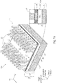
Figs. 1 and1a show semiconductor devices according to examples. -
Fig. 2 shows a field distribution for the device inFig. 1a . -
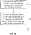
Fig. 2a shows a method for confining radiation according to an example. -
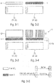
Figs. 3-1 to 3-6 show steps for a method for manufacturing a semiconductor device according to examples. -
Fig. 4 shows a scheme of a gas sensor according to an example. -
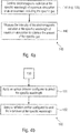
Fig. 4a shows a method for measuring the quantiy of a gas according to an example. -
Fig. 4b shows a method for manufacturing a gas sensor as that ofFig. 4 . -
Fig. 1 shows a semiconductor device 10. The semiconductor device 10 may be used, for example, for a gas sensor, but other applications may be possible. The semiconductor device (or the gas sensor) may be or be contained in an on-chip device. The semiconductor device (or the gas sensor) may be or be contained in a package-like device. - The semiconductor device 10 may comprise a pillar
photonic crystal 11, having astructure 13 and a plurality of pillars (rods) 12 extending from thestructure 13. Thestructure 13 may be mainly developed along a plane (here represented as a horizontal plane), which is here represented as being associated to (e.g., generated by) axes x and y. The horizontal plane x, y may be parallel to the main planes along which the chip or package is developed. Thepillars 12 may extend in a height direction (here represented as a vertical direction), which is represented inFig. 1 by axis z. The axis z may be perpendicular to axes x, y. - The
structure 13 may be a layered structure. The layers of thestructure 13 may each have a thickness which may be measured in the height (vertical) direction (axis z). In case the semiconductor device 10 is used for a gas sensor, thespace 17 free from thestructure 13 and thepillars 12 may be replenished by a mixture of gasses in which the amount of a specific gas is to be measured among other gasses. - Structural properties of the pillars 12 (e.g., geometrical properties and/or properties associated to the material, such as the refraction index) may be associated to a specific wavelength of radiation, wherein the radiation at the specific wavelength is to be contained in at least one planar direction (e.g., lateral direction). The distances between
consecutive pillars 12 and their diameters may be chosen so as to perform a lateral confinement for one narrow range of radiations (e.g., a wavelength or specific wavelengths), hence prohibiting the propagation of the radiation at a specific wavelength in the lateral direction. The array of pillars may be periodical, e.g., in one or two planar directions, the distance between two consecutive pillars representing the spatial period in one or two planar directions. The array of pillars may be bidimensional, forming a matrix of pillars. Thepillars 12 are displaced (e.g., as an array) to form a spatially periodic variation in the refractive index in the intent of forbidding propagation of the specific wavelength of the electromagnetic radiation (e.g., infra-red, IR, rays and/or visible light) in at least the lateral direction. - In examples, the material for the
pillars 12 may be or comprise silicon (e.g., poly-silicon). In examples, the structural properties of thepillars 12 are such that the specific wavelength to be trapped is 4.26 µm, which is the wavelength of maximum absorption of carbon dioxide (CO2). The period in one direction (e.g., in the direction of propagation according to the wavelength) may be, for example, a multiple of the specific wavelength(s) to be trapped (e.g., 4.26 µm). Other wavelengths (e.g., in the mid-IR region or in the visible light region) may be chosen (e.g., for obtaining gas sensors which are sensitive to gasses different from carbon dioxide). - The semiconductor device 10 may comprise a
waveguide 15, Thewaveguide 15 may be formed by the absence ofpillars 12, which may be, for example, displaced along a propagation direction. As can be seen fromFig. 1 , the propagation direction is a planar direction in the sense that is in the plane x, y, but is not necessarily coincident with any of axes x and y. While radiation is in general allowed to propagate in the propagation direction of the waveguide, only radiation at the specific wavelength is forbidden from propagating in a lateral direction perpendicular to the propagation direction. Both the propagation direction and the lateral direction are planar directions which may be coincident to (or may be linearly dependent from) the axes x and y inFig. 1 . Therefore, radiation at the specific wavelength (as defined by the array of pillars 12) may be trapped laterally but may propagate along the propagation direction defined by thewaveguide 15. - It has been noted that, by implementing the
structure 13 to include a confininglayer 14, a vertical confinement of the radiation at the specific wavelength may be obtained, hence increasing the efficiency of thephotonic crystal 11. - In particular, it has been understood that it is possible to confine the radiation at the specific wavelength by exciting surface plasmon polaritons (SPPs).
- SPPs are IR or visible-frequency electromagnetic waves propagating along an interface between the
structure 13 and the space 17 (which is replenished with gas or a mixture of gas). SPPs involve both charge motion in the highly doped semiconductor material ("surface plasmon") and electromagnetic waves in the space 17 ("polaritons"). The surface plasmon is a surficial oscillation of free electrons in the highly doped semiconductor material of the confininglayer 14. SPPs are surface waves, guided along the interface, e.g., in a way similar to that according to which light is guided by an optical fiber. SPPs present tighter spatial confinement and higher local field intensity. - Therefore, while the propagation of the radiation at the specific wavelength in the planar directions (both the propagation direction and the lateral direction) is governed by the effect of the photonic crystal as operated by the array of
pillars 12, the vertical propagation is prevented by the SPPs. - The confining
layer 14 may be, for example, made of highly doped semiconductor material. The concentration of charges may be in the range between 1019 cm-3 and 1021 cm-3. The charges may be, for example, negative charges. The confininglayer 14 may be, for example, a thin film. The confining layer may have a thickness of less than 400 nm, or, more preferably, between 50 nm and 100 nm, e.g., 100 nm or about 100 nm. The preferred material may be silicon. - The complex relative permittivity (e.g., expressed as a ratio relative to the complex permittivity of the vacuum) may be in general expressed with εr(ω)= ε'r(ω) +jε"r(ω), where ω is the pulse (2π-times the frequency of the radiation), ε'r(ω) is the real part, and ε'r(ω) is the imaginary part. In particular in the mid-IR region (e.g., around 4.26 µm), the semiconductor material may be chosen so as to have the real part ε'r(ω) to be negative (ε'r(ω)<0) and/or to have the imaginary part ε"r(ω) to be a value (e.g., in the range between -1 and 0, e.g. -1<ε"r(ω<0) which does not cause excessive damping.
- By vertically confining the radiation because of the SPPs, it is also possible to define the heights of the
pillars 12 so as to be associated to specific wavelength of the radiation to be confined. Accordingly, the height of thepillars 12 in the height direction (axis z) may be the length, or more in general may be associated to the length (e.g., a multiple value) of a vertical mode distribution of the electromagnetic radiation at the specific wavelength. For example, the height of the pillars 12 (from the surface of thestructure 13 to the summity of each pillar 12) may be between 6λ0 and 14λ0, or preferably, between 8λ0 and 12λ0, or more preferably 10λ0 or around 10λ0 (where λ0 is the particular specific wavelength of the radiation to be confined), without considering the SPP. - By defining the height of the
pillars 12 in association to the length of a vertical mode distribution of the electromagnetic radiation at the specific wavelength, the advantage is attained that the height of thepillars 12 may be reduced; otherwise, in an attempt to increase vertical confinement, the height of thepillars 12 would be increased, up to a point of causing difficulties in the production of the pillars 10. Hence, the aspect ratio may be less challenging than in the prior art. - As can be seen from
Fig. 1 , the layeredstructure 13 may comprise at least one of the following layers: - a
substrate layer 25, which may comprise:- ∘ a
first substrate sublayer 21, e.g., in silicon; - ∘ a
second substrate sublayer 22, e.g., in silicon dioxide;
- ∘ a
- a highly doped
confinement layer 14; - a thin non-doped semiconductor layer 23 (e.g., in silicon dioxide).
- The
pillars 12 may therefore protrude from the thinnon-doped semiconductor layer 23 or protrude from the highly dopedconfinement layer 14. - A variant to the device 10 of
Fig. 1 is thedevice 10a ofFig. 1a . Here, thelayered structure 13a does not comprise the thinnon-doped semiconductor layer 23. Thelayered structure 13a may comprise at least one of the following layers: - a
substrate layer 25, which may comprise:- ∘ a
first substrate sublayer 21, e.g., in silicon; - ∘ a
second substrate sublayer 22, e.g., in silicon dioxide;
- ∘ a
- a highly doped
confinement layer 14. - The
pillars 12 may therefore protrude from thesecond substrate sublayer 22 and the highly dopedconfinement layer 14 siting between them or protrude from the highly dopedconfinement layer 14. - The remaining features of the
device 10a may be like at least some of the features of the device 10 and are therefore not repeated. - A simulation on
device 10a ofFig. 1a has been performed.Fig. 2 shows a distribution 20 of the squared field intensity E2 in correspondence to thewaveguide 15. The areas which are different from the area 20 correspond to field intensity which may be approximated to zero. The successful vertical confinement may be appreciated. - As shown by
Fig. 2 , it is possible to perform (e.g., using equipment discussed above and/or below) amethod 120 for spatially confining electromagnetic radiation at a specific wavelength, the method comprising: - (step 121) confining the electromagnetic radiation in a lateral direction through a pillar array (e.g., 12) extending in a height direction (e.g., z) so as to form a photonic crystal (e.g., 11); and/or
- (step 122) confining the electromagnetic radiation in a height direction (e.g., z) by plasmonic effect, through a confinement layer (e.g., 14) extending in a planar direction perpendicular to the height direction (e.g., z), the confinement layer (e.g., 14) being in doped semiconductor material.
- The method may permit the electromagnetic radiation at specific wavelength(s) (e.g. 4.26 µm) to propagate according to a propagation direction defined by a waveguide (e.g., 15).
-
Figs. 3-1 to 3-6 show steps for manufacturing a semiconductor device such as thedevice 10 or 10a. In the passages, thedevice 10 or 10a is shown as vertically exploded to increase intelligibility.Figs. 3-5 and3-6 resume the passages. - According to a method, a substrate layer may be made. In particular, a
first substrate sublayer 21 and asecond substrate sublayer 22 over thefirst substrate layer 21 may be made. -
Fig. 3-1 shows thesubstrate layer 25 which may be formed by thefirst substrate sublayer 21 and thesecond substrate layer 22. - The
first substrate sublayer 21 may be in non-doped semiconductor material (e.g., silicon). - The
second substrate layer 22 may be in silicon dioxide (which may be used to prevent the migration of dopants from the highly dopedlayer 14, to be prepared subsequently). - Over the substrate layer 25 (21, 22), a semiconductor layer 14' in semiconductor material (e.g., silicon) may deposited or otherwise made. The semiconductor layer 14' may be the precursor of the
confinement layer 14. - In the transition towards
Fig. 3-2 , the layer 14' may be doped, to obtain a highly dopedlayer 14, which may be theconfinement layer 14 discussed above for supporting SPPs. For example, the doping may arrive at a concentration of charges in the range between 1019 cm-3 and 1021 cm-3. - In the transition towards
Fig. 3-3 , a thin non-doped semiconductor layer 23 (e.g., in silicon dioxide) may be deposed over the highly doped layer (confinement layer) 14. The thin sublayer 23 (not shown inFigs. 3-1 to 3-4 ) may be used to prevent the migration of dopants from the highly doped layer 14 (e.g., towards a subsequent non-doped semiconductor layer to be deposed subsequently). The thinnon-doped semiconductor layer 23 may operate as a stop layer for performing the etching step that will form thepillars 12. The thinnon-doped semiconductor layer 23 may help to confine SPP mode into the surface. The thinnon-doped semiconductor layer 23 may be used for manufacturing the device 10 ofFig. 1 . In alternative, when manufacturing thedevice 10a ofFig. 1a , no step for making the thinnon-doped semiconductor layer 23 is provided. - A thick non-doped semiconductor layer 12' (e.g., in polysilicon) may be deposited over the thin
non-doped semiconductor layer 22 and/or over the highly doped layer (confinement layer) 14. The thick non-doped semiconductor layer 12' may be the precursor of the pillars (rods) 12. The thickness of the thick non-doped semiconductor layer 12' may therefore be that of (or otherwise associated to) the vertical confinement length of the mode of the radiation to be vertically confined. - In the transition towards
Fig. 3-4 , material is selectively removed from the thick non-doped semiconductor layer 12', to obtain a pattern ofpillars 12. The etching may be performed, e.g., in such a way to present mutual distances and/or diameters which permit lateral confinement according to bandgap engineering. Etching (e.g., dry etching) may be used. Photolithography techniques may be used. - Accordingly, a device such as the
semiconductor device 10 or 10a may be obtained. The step of removing can be performed with higher reliability, as thepillars 12 have a reduced height as compared to the pillars that should be necessary for vertically containing the radiation without the use of the present techniques. - More in general, a
manufacturing method 130 may comprise at least one of the following steps (shown inFig. 3-6 ): - doping a layer of a semiconductor (step 131), e.g., doping layer 14', to obtain a highly doped
layer 14; - depositing a non-doped layer of semiconductor over the doped layer of semiconductor (step 132), e.g., depositing the layer 12' which is the precursor of the
pillars 12; - selectively removing material from the non-doped layer of semiconductor 12' so as to obtain an array of pillars which form a photonic crystal for a specific wavelength (step 133), e.g., to arrive at the formation of the array of
pillars 12. - Methods above may be performed using techniques such as silicon-on-insulator, SOI, techniques.
-
Fig. 4 shows agas sensor 40, which may be a mid-IR gas sensor. Thegas sensor 40 that may make use of thesemiconductor device 10 or 10a. Thegas sensor 40 may comprise asemiconductor device 10 or 10a with thephotonic crystal 11 and/or thewaveguide 15. Thegas sensor 40 may be used to measure, for example, the amount of a specific gas (e.g., within a mixture of gasses). - The
gas sensor 40 may comprise a generator (radiation source) 41 upstream to thesemiconductor device 10 or 10a. Theradiation source 41 may generate or emit (e.g., by filtering generated light) electromagnetic radiation (e.g., IR or visible light). The electromagnetic radiation may be generated at the specific wavelength or may be otherwise filtered. - In the semiconductor device 10 and in particular in the
space 17 and mainly within thewaveguide 15, a specific gas to be measured or a mixture of gasses containing the specific gas may be present. The specific gas may interact with the radiation. The specific wavelength of the radiation, propagating through thewaveguide 17, may be the wavelength of maximum absorption of the specific gas. - The
optical gas sensor 40 may comprise an optical detector 42 detecting electromagnetic radiation at the specific wavelength. - By detecting the electromagnetic radiation at the specific wavelength (e.g., by comparing the intensity of radiation at the specific wavelength as generated by the
radiation source 41 and the intensity of radiation at the specific wavelength as detected by the detector 42), it is possible to determine (e.g., estimate) the amount of the specific gas. These operations may be performed by acontroller 43, which may be a device which controls theradiation source 41 and which obtains the intensity information from the optical detector 42. The controller may be or comprise a digital equipment, such as a processor, which may be a digital signal processor, DSP. - There is the possibility of performing (e.g., by using at least part of the equipment such as that discussed above) a
method 140 for measuring a quantity of specific gas, the specific gas being associated to a specific wavelength of maximum absorption. Themethod 140 may comprise at least one of: - confining, at least in a lateral direction and a vertical direction, the electromagnetic radiation at the specific wavelength of maximum absorption in an environment (e.g.,
space 17 or waveguide 15) including the specific gas (step 141, e.g., which may be implemented by method 130); - measuring the intensity of the electromagnetic radiation at the specific wavelength of maximum absorption to estimate the amount of the specific gas (step 142).
- The measured intensity may be used to determine the quantity (amount) of the gas in the environment (e.g., 15). For example, the detected intensity may be compared to emitted intensity, so as to estimate the amount of the specific gas.
- Reference has been made, above, to a sensor for sensing carbon dioxide. However, other gasses may be sensed, by opportunely choosing the structural and/or functional features of the
semiconductor device 10 or 10a and/or thegas sensor 40. The following is a non-exhaustive list of wavelengths that can be used for determining the amount of each material (source: Wikipedia). - O2: 0.763 µm
- CO2: 4.26 µm, 2.7 µm, about 13 µm
- CO: 4.67 µm, 1.55 µm, 2.33 µm, 4.6 µm, 4.8 µm, 5.9 µm
- NO2 - 6.17-6.43 µm, 15.4-16.3 µm, 496 nm
- N2O - 7.73 µm, 1.52 µm, 4.3 µm, 4.4 µm, about 8 µm
- HNO3 - 5.81 µm
- NH3 - 2.25 µm, 3.03 µm, 5.7 µm
- H2S - 1.57 µm, 3.72 µm, 3.83 µm
- SO2 - 7.35 µm, 19.25 µm
- HF - 1.27 µm, 1.33 µm
- HCl - 3.4 µm
- HBr - 1.34 µm, 3.77 µm
- HI - 4.39 µm
- hydrocarbons - 3.3-3.5 µm, the C-H bond vibration
- CH4 - 3.33 µm, 7.91±0.16 µm can also be used, 1.3 µm, 1.65 µm, 2.3 µm, 3.2-3.5 µm, about 7.7 µm
- C2H2 - 3.07 µm
- C3H8 - 1.68 µm, 3.3 µm
- CH3Cl - 3.29 µm
- H2O - 1.94 µm, 2.9 µm
- O3 - 9.0 µm, also 254 nm (UV)
- H2O2 - 7.79 µm
- alcohol mixtures - 9.5±0.45 µm
- HCHO-3.6 µm
- HCOOH - 8.98 µm
- COS - 4.87 µm
- A
method 150 for manufacturing thegas sensor 40 may by performed by at least one of the following steps: - performing the
method 130 to obtain a semiconductor device having a photonic crystal as above; and - applying an optical detector configured to detect the specific wavelength (step 151); and/or
- applying a radiation source (e.g., 41) configured to emit the radiation at the specific wavelength (step 152).
- Methods of operating the
gas sensor 40 and/or thesemiconductor device 10 or 10a may be performed under the control of a processor (e.g., the controller 43). In particular, a non-transitory storage unit may contain instructions which, when executed by a processor, cause the processor to control a method above and/or thegas sensor 40 and/or the semiconductor device 10. - In examples, above, when referring to a particular wavelength, reference may be made to a narrowband containing the particular wavelength (e.g., with a tolerance of 1%, or 0.1%, or 0.01%, or even less, for example). The same may apply to the constructional features, such as heights and other measures.
- In examples above, reference has always been made to array of pillars. This definition also comprises bidimensional arrays, i.e. matrixes, such as in
Fig. 1 . - The implementation in hardware or in software may be performed using a digital storage medium, for example cloud storage, a floppy disk, a DVD, a Blue-Ray, a CD, a ROM, a PROM, an EPROM, an EEPROM or a FLASH memory, having electronically readable control signals stored thereon, which cooperate (or are capable of cooperating) with a programmable computer system such that the respective method is performed. Therefore, the digital storage medium may be computer readable.
- Some examples comprise a data carrier having electronically readable control signals, which are capable of cooperating with a programmable computer system, such that one of the methods described herein is performed.
- Generally, examples may be implemented as a computer program product with a program code, the program code being operative for performing one of the methods when the computer program product runs on a computer. The program code may for example be stored on a machine-readable carrier.
- Other examples comprise the computer program for performing one of the methods described herein, stored on a machine-readable carrier. In other words, an example is, therefore, a computer program having a program code for performing one of the methods described herein, when the computer program runs on a computer.
- A further example is, therefore, a data carrier (or a digital storage medium, or a computer-readable medium) comprising, recorded thereon, the computer program for performing one of the methods described herein. A further example is, therefore, a data stream or a sequence of signals representing the computer program for performing one of the methods described herein. The data stream or the sequence of signals may for example be configured to be transferred via a data communication connection, for example via the Internet. A further example comprises a processing means, for example a computer, or a programmable logic device, configured to or adapted to perform one of the methods described herein. A further example comprises a computer having installed thereon the computer program for performing one of the methods described herein.
- In some examples, a programmable logic device (for example a field programmable gate array) may be used to perform some or all of the functionalities of the methods described herein. In some examples, a field programmable gate array may cooperate with a microprocessor in order to perform one of the methods described herein. Generally, the methods are preferably performed by any hardware apparatus.
- The above described examples are merely illustrative for the principles above. It is understood that modifications and variations of the arrangements and the details described herein will be apparent to others skilled in the art. It is the intent, therefore, to be limited only by the scope of the impending patent claims and not by the specific details presented by way of description and explanation of the examples herein.
Claims (15)
- A semiconductor device (10, 10a), comprising:a pillar photonic crystal (11) including a structure (13, 13a) and a plurality of pillars (12) extending from the structure (13, 13a) in a height direction (z),wherein the plurality of pillars (12) form at least one waveguide (15) for electromagnetic radiation at a specific wavelength, the at least one waveguide (15) extending in at least one planar direction,wherein the structure (13, 13a) includes a confining layer (14) in doped semiconductor material to support propagation of surface plasmon polaritons.
- The semiconductor device (10, 10a) of claim 1,
wherein the height of the pillars (12) in the height direction (z) is associated to the length of a vertical mode distribution of the electromagnetic radiation at the specific wavelength. - The semiconductor device (10, 10a) of claim 1 or 2,
wherein the confining layer (14) has a thickness of between 50 nm and 150 in the height direction (z). - The semiconductor device (10, 10a) of any of the preceding claims,
wherein the relative permittivity of the doped semiconductor of the confinement layer (14) is negative. - The semiconductor device (10, 10a) of any of the preceding claims,
wherein the imaginary part of the relative permittivity of the doped semiconductor is between -1 and 0. - The semiconductor device (10, 10a) of any of the preceding claims,
wherein the specific wavelength is 4.26 µm. - The semiconductor device (10, 10a) of any of the preceding claims,
wherein the specific wavelength is in the mid-infrared, IR, region. - The semiconductor device (10, 10a) of any of the preceding claims,
wherein the semiconductor material of the confinement layer (14) has a concentration of charges between 1019 cm-3 and 1021 cm-3. - An optical gas sensor (40) for measuring the amount of a specific gas, comprising:the semiconductor device (10, 10a) of any of the preceding claim; andan optical detector (42) to detect electromagnetic radiation at the specific wavelength, wherein the specific wavelength is the wavelength of maximum absorption of the specific gas; andthe optical detector (42) is configured to measure the intensity of the electromagnetic radiation at the specific wavelength,so that the optical gas sensor (40) determines the amount of the specific gas on the basis of the intensity of the electromagnetic radiation.
- A method for spatially confining electromagnetic radiation at a specific wavelength, the method comprising:confining the electromagnetic radiation in a lateral direction through a pillar array (12) extending in a height direction (z) and forming a photonic crystal (11); andconfining the electromagnetic radiation in a height direction (z) by plasmonic effect, through a confinement layer (14) extending in a planar direction perpendicular to the height direction (z), the confinement layer (14) being in doped semiconductor material.
- A method for measuring a quantity of specific gas, the specific gas being associated to a specific wavelength of maximum absorption, the method comprising:confining the electromagnetic radiation at the specific wavelength of maximum absorption according to claim 10 in an environment including the specific gas; andmeasuring the intensity of the electromagnetic radiation at the specific wavelength of maximum absorption to estimate the amount of the specific gas.
- A method for manufacturing a semiconductor device (10, 10a), comprising:doping a layer (14') of a semiconductor;depositing a non-doped layer (12') of semiconductor over the doped layer (14) of semiconductor; andselectively removing material from the non-doped layer (14) of semiconductor so as to obtain an array of pillars (12) forming a photonic crystal for a specific wavelength.
- The method of claim 12,
wherein the step of depositing the non-doped layer (12') of semiconductor includes depositing the non-doped layer (12') to have a thickness which is the length or a multiple of the length of a vertical mode distribution of the electromagnetic radiation at the specific wavelength. - A method for manufacturing an optical gas sensor for measuring the amount of a specific gas, the method comprising:performing the method of any of claims 12 or 13; andapplying an optical detector (42) configured to detect the specific wavelength.
- A non-transitory storage unit containing instructions which, when executed by a processor, cause the processor to control the method of claim 10 or 11.
Priority Applications (2)
| Application Number | Priority Date | Filing Date | Title |
|---|---|---|---|
| EP19167125.4A EP3718963B1 (en) | 2019-04-03 | 2019-04-03 | Pillar photonic crystal |
| US16/817,874 US11067500B2 (en) | 2019-04-03 | 2020-03-13 | Pillar photonic crystal |
Applications Claiming Priority (1)
| Application Number | Priority Date | Filing Date | Title |
|---|---|---|---|
| EP19167125.4A EP3718963B1 (en) | 2019-04-03 | 2019-04-03 | Pillar photonic crystal |
Publications (2)
| Publication Number | Publication Date |
|---|---|
| EP3718963A1 true EP3718963A1 (en) | 2020-10-07 |
| EP3718963B1 EP3718963B1 (en) | 2024-09-04 |
Family
ID=66102866
Family Applications (1)
| Application Number | Title | Priority Date | Filing Date |
|---|---|---|---|
| EP19167125.4A Active EP3718963B1 (en) | 2019-04-03 | 2019-04-03 | Pillar photonic crystal |
Country Status (2)
| Country | Link |
|---|---|
| US (1) | US11067500B2 (en) |
| EP (1) | EP3718963B1 (en) |
Citations (4)
| Publication number | Priority date | Publication date | Assignee | Title |
|---|---|---|---|---|
| US20050084195A1 (en) * | 2003-10-15 | 2005-04-21 | Hamann Hendrik F. | Method and apparatus for forming lateral electrical contacts for photonic crystal devices |
| US20050281524A1 (en) * | 2004-06-22 | 2005-12-22 | Chandra Mouli | Photonic crystal-based optical elements for integrated circuits and methods therefor |
| WO2006007446A2 (en) * | 2004-06-17 | 2006-01-19 | Ion Optics, Inc. | Photonic crystal emitter, detector, and sensor |
| US20090002701A1 (en) * | 2007-06-26 | 2009-01-01 | Fattal David A | Electric-field-enhancement structure and detection apparatus using same |
Family Cites Families (3)
| Publication number | Priority date | Publication date | Assignee | Title |
|---|---|---|---|---|
| US6859304B2 (en) * | 2002-08-09 | 2005-02-22 | Energy Conversion Devices, Inc. | Photonic crystals and devices having tunability and switchability |
| EP2261638B8 (en) * | 2008-03-28 | 2015-04-15 | Horiba, Ltd.g | Wavelength stabilized laser device for an analyzer |
| EP2488912B1 (en) * | 2009-10-12 | 2019-07-24 | The Trustees Of Columbia University In The City Of New York | Waveguide comprising photonic crystal for outcoupling light of specific wavelengths |
-
2019
- 2019-04-03 EP EP19167125.4A patent/EP3718963B1/en active Active
-
2020
- 2020-03-13 US US16/817,874 patent/US11067500B2/en active Active
Patent Citations (4)
| Publication number | Priority date | Publication date | Assignee | Title |
|---|---|---|---|---|
| US20050084195A1 (en) * | 2003-10-15 | 2005-04-21 | Hamann Hendrik F. | Method and apparatus for forming lateral electrical contacts for photonic crystal devices |
| WO2006007446A2 (en) * | 2004-06-17 | 2006-01-19 | Ion Optics, Inc. | Photonic crystal emitter, detector, and sensor |
| US20050281524A1 (en) * | 2004-06-22 | 2005-12-22 | Chandra Mouli | Photonic crystal-based optical elements for integrated circuits and methods therefor |
| US20090002701A1 (en) * | 2007-06-26 | 2009-01-01 | Fattal David A | Electric-field-enhancement structure and detection apparatus using same |
Also Published As
| Publication number | Publication date |
|---|---|
| US20200319095A1 (en) | 2020-10-08 |
| EP3718963B1 (en) | 2024-09-04 |
| US11067500B2 (en) | 2021-07-20 |
Similar Documents
| Publication | Publication Date | Title |
|---|---|---|
| US9176059B2 (en) | Optical analyte sensor | |
| US8170388B2 (en) | Method for effective refractive index trimming of optical waveguiding structures and optical waveguiding structures | |
| US20110116094A1 (en) | Method of Producing a Surface Plasmon Generator, a Surface Plasmon Generator and a Sensor Incorporating the Surface Plasmon Generator | |
| JPH0572432A (en) | Single-mode space-integrated optical filter and executing method thereof | |
| CN109323661A (en) | High Sensitivity Angular Displacement Sensor Based on Beam Spatial Guss-Hansen Displacement | |
| Chiang et al. | Effects of temperature on the surface plasmon resonance at a metal–semiconductor interface | |
| CN103091268B (en) | Multi-component gas concentration measurement method based on photonic crystal groove waveguide | |
| Yan et al. | A fast response hydrogen sensor with Pd metallic grating onto a fiber's end-face | |
| Brenny et al. | Near-infrared spectroscopic cathodoluminescence imaging polarimetry on silicon photonic crystal waveguides | |
| US11067500B2 (en) | Pillar photonic crystal | |
| CN114594051B (en) | A methane gas sensor and monitoring system based on optical materials | |
| Tarumaraja et al. | FDTD numerical analysis of SPR sensing using graphene-based photonic crystal | |
| US12094899B2 (en) | Metasurfaces for high-efficient IR photodetectors | |
| CN104316498B (en) | A kind of Terahertz sensor of surface plasma body resonant vibration | |
| Buchberger et al. | Single particle detector using the evanescent field of a silicon nitride waveguide | |
| EP4594734A1 (en) | Selective gas sensor | |
| CN113534298B (en) | Photonic crystal capable of realizing larger negative Goos-Hansen displacement | |
| Taliercio et al. | Plasmonic bio-sensing based on highly doped semiconductors | |
| US20260133131A1 (en) | Optical sensor for detecting caesium ions and/or measuring concentration of the same | |
| Hasan et al. | Decision Making Using Analytic Hierarchy Process for Plasmonic Waveguide Simulated by Finite-Difference Eigenmode Method | |
| Yardley | Design and characterization of organic waveguides for passive and active optical devices | |
| CN103969220A (en) | Method for detecting dynamic optical properties of UV (Ultraviolet) glue in curing process | |
| Rabelink | Photonic crystal nanocavities on fiber tips: design and characterization | |
| Jannesari et al. | Vertical coupling into a photonic crystal waveguide using band folding design | |
| Schmid et al. | Applications of subwavelength grating structures in silicon-on-insulator waveguides |
Legal Events
| Date | Code | Title | Description |
|---|---|---|---|
| PUAI | Public reference made under article 153(3) epc to a published international application that has entered the european phase |
Free format text: ORIGINAL CODE: 0009012 |
|
| STAA | Information on the status of an ep patent application or granted ep patent |
Free format text: STATUS: THE APPLICATION HAS BEEN PUBLISHED |
|
| AK | Designated contracting states |
Kind code of ref document: A1 Designated state(s): AL AT BE BG CH CY CZ DE DK EE ES FI FR GB GR HR HU IE IS IT LI LT LU LV MC MK MT NL NO PL PT RO RS SE SI SK SM TR |
|
| AX | Request for extension of the european patent |
Extension state: BA ME |
|
| STAA | Information on the status of an ep patent application or granted ep patent |
Free format text: STATUS: REQUEST FOR EXAMINATION WAS MADE |
|
| 17P | Request for examination filed |
Effective date: 20201029 |
|
| RBV | Designated contracting states (corrected) |
Designated state(s): AL AT BE BG CH CY CZ DE DK EE ES FI FR GB GR HR HU IE IS IT LI LT LU LV MC MK MT NL NO PL PT RO RS SE SI SK SM TR |
|
| STAA | Information on the status of an ep patent application or granted ep patent |
Free format text: STATUS: EXAMINATION IS IN PROGRESS |
|
| 17Q | First examination report despatched |
Effective date: 20210818 |
|
| GRAP | Despatch of communication of intention to grant a patent |
Free format text: ORIGINAL CODE: EPIDOSNIGR1 |
|
| STAA | Information on the status of an ep patent application or granted ep patent |
Free format text: STATUS: GRANT OF PATENT IS INTENDED |
|
| GRAJ | Information related to disapproval of communication of intention to grant by the applicant or resumption of examination proceedings by the epo deleted |
Free format text: ORIGINAL CODE: EPIDOSDIGR1 |
|
| STAA | Information on the status of an ep patent application or granted ep patent |
Free format text: STATUS: EXAMINATION IS IN PROGRESS |
|
| INTG | Intention to grant announced |
Effective date: 20240311 |
|
| GRAP | Despatch of communication of intention to grant a patent |
Free format text: ORIGINAL CODE: EPIDOSNIGR1 |
|
| STAA | Information on the status of an ep patent application or granted ep patent |
Free format text: STATUS: GRANT OF PATENT IS INTENDED |
|
| INTC | Intention to grant announced (deleted) | ||
| INTG | Intention to grant announced |
Effective date: 20240408 |
|
| P01 | Opt-out of the competence of the unified patent court (upc) registered |
Effective date: 20240507 |
|
| GRAS | Grant fee paid |
Free format text: ORIGINAL CODE: EPIDOSNIGR3 |
|
| GRAA | (expected) grant |
Free format text: ORIGINAL CODE: 0009210 |
|
| STAA | Information on the status of an ep patent application or granted ep patent |
Free format text: STATUS: THE PATENT HAS BEEN GRANTED |
|
| AK | Designated contracting states |
Kind code of ref document: B1 Designated state(s): AL AT BE BG CH CY CZ DE DK EE ES FI FR GB GR HR HU IE IS IT LI LT LU LV MC MK MT NL NO PL PT RO RS SE SI SK SM TR |
|
| REG | Reference to a national code |
Ref country code: GB Ref legal event code: FG4D |
|
| REG | Reference to a national code |
Ref country code: CH Ref legal event code: EP |
|
| REG | Reference to a national code |
Ref country code: IE Ref legal event code: FG4D |
|
| REG | Reference to a national code |
Ref country code: DE Ref legal event code: R096 Ref document number: 602019058179 Country of ref document: DE |
|
| REG | Reference to a national code |
Ref country code: LT Ref legal event code: MG9D |
|
| REG | Reference to a national code |
Ref country code: NL Ref legal event code: MP Effective date: 20240904 |
|
| PG25 | Lapsed in a contracting state [announced via postgrant information from national office to epo] |
Ref country code: NO Free format text: LAPSE BECAUSE OF FAILURE TO SUBMIT A TRANSLATION OF THE DESCRIPTION OR TO PAY THE FEE WITHIN THE PRESCRIBED TIME-LIMIT Effective date: 20241204 |
|
| PG25 | Lapsed in a contracting state [announced via postgrant information from national office to epo] |
Ref country code: PL Free format text: LAPSE BECAUSE OF FAILURE TO SUBMIT A TRANSLATION OF THE DESCRIPTION OR TO PAY THE FEE WITHIN THE PRESCRIBED TIME-LIMIT Effective date: 20240904 Ref country code: FI Free format text: LAPSE BECAUSE OF FAILURE TO SUBMIT A TRANSLATION OF THE DESCRIPTION OR TO PAY THE FEE WITHIN THE PRESCRIBED TIME-LIMIT Effective date: 20240904 Ref country code: GR Free format text: LAPSE BECAUSE OF FAILURE TO SUBMIT A TRANSLATION OF THE DESCRIPTION OR TO PAY THE FEE WITHIN THE PRESCRIBED TIME-LIMIT Effective date: 20241205 |
|
| PG25 | Lapsed in a contracting state [announced via postgrant information from national office to epo] |
Ref country code: BG Free format text: LAPSE BECAUSE OF FAILURE TO SUBMIT A TRANSLATION OF THE DESCRIPTION OR TO PAY THE FEE WITHIN THE PRESCRIBED TIME-LIMIT Effective date: 20240904 |
|
| PG25 | Lapsed in a contracting state [announced via postgrant information from national office to epo] |
Ref country code: LV Free format text: LAPSE BECAUSE OF FAILURE TO SUBMIT A TRANSLATION OF THE DESCRIPTION OR TO PAY THE FEE WITHIN THE PRESCRIBED TIME-LIMIT Effective date: 20240904 |
|
| PG25 | Lapsed in a contracting state [announced via postgrant information from national office to epo] |
Ref country code: HR Free format text: LAPSE BECAUSE OF FAILURE TO SUBMIT A TRANSLATION OF THE DESCRIPTION OR TO PAY THE FEE WITHIN THE PRESCRIBED TIME-LIMIT Effective date: 20240904 |
|
| PG25 | Lapsed in a contracting state [announced via postgrant information from national office to epo] |
Ref country code: ES Free format text: LAPSE BECAUSE OF FAILURE TO SUBMIT A TRANSLATION OF THE DESCRIPTION OR TO PAY THE FEE WITHIN THE PRESCRIBED TIME-LIMIT Effective date: 20240904 Ref country code: RS Free format text: LAPSE BECAUSE OF FAILURE TO SUBMIT A TRANSLATION OF THE DESCRIPTION OR TO PAY THE FEE WITHIN THE PRESCRIBED TIME-LIMIT Effective date: 20241204 |
|
| PG25 | Lapsed in a contracting state [announced via postgrant information from national office to epo] |
Ref country code: RS Free format text: LAPSE BECAUSE OF FAILURE TO SUBMIT A TRANSLATION OF THE DESCRIPTION OR TO PAY THE FEE WITHIN THE PRESCRIBED TIME-LIMIT Effective date: 20241204 Ref country code: PL Free format text: LAPSE BECAUSE OF FAILURE TO SUBMIT A TRANSLATION OF THE DESCRIPTION OR TO PAY THE FEE WITHIN THE PRESCRIBED TIME-LIMIT Effective date: 20240904 Ref country code: NO Free format text: LAPSE BECAUSE OF FAILURE TO SUBMIT A TRANSLATION OF THE DESCRIPTION OR TO PAY THE FEE WITHIN THE PRESCRIBED TIME-LIMIT Effective date: 20241204 Ref country code: LV Free format text: LAPSE BECAUSE OF FAILURE TO SUBMIT A TRANSLATION OF THE DESCRIPTION OR TO PAY THE FEE WITHIN THE PRESCRIBED TIME-LIMIT Effective date: 20240904 Ref country code: HR Free format text: LAPSE BECAUSE OF FAILURE TO SUBMIT A TRANSLATION OF THE DESCRIPTION OR TO PAY THE FEE WITHIN THE PRESCRIBED TIME-LIMIT Effective date: 20240904 Ref country code: GR Free format text: LAPSE BECAUSE OF FAILURE TO SUBMIT A TRANSLATION OF THE DESCRIPTION OR TO PAY THE FEE WITHIN THE PRESCRIBED TIME-LIMIT Effective date: 20241205 Ref country code: FI Free format text: LAPSE BECAUSE OF FAILURE TO SUBMIT A TRANSLATION OF THE DESCRIPTION OR TO PAY THE FEE WITHIN THE PRESCRIBED TIME-LIMIT Effective date: 20240904 Ref country code: ES Free format text: LAPSE BECAUSE OF FAILURE TO SUBMIT A TRANSLATION OF THE DESCRIPTION OR TO PAY THE FEE WITHIN THE PRESCRIBED TIME-LIMIT Effective date: 20240904 Ref country code: BG Free format text: LAPSE BECAUSE OF FAILURE TO SUBMIT A TRANSLATION OF THE DESCRIPTION OR TO PAY THE FEE WITHIN THE PRESCRIBED TIME-LIMIT Effective date: 20240904 |
|
| REG | Reference to a national code |
Ref country code: AT Ref legal event code: MK05 Ref document number: 1720233 Country of ref document: AT Kind code of ref document: T Effective date: 20240904 |
|
| PG25 | Lapsed in a contracting state [announced via postgrant information from national office to epo] |
Ref country code: NL Free format text: LAPSE BECAUSE OF FAILURE TO SUBMIT A TRANSLATION OF THE DESCRIPTION OR TO PAY THE FEE WITHIN THE PRESCRIBED TIME-LIMIT Effective date: 20240904 |
|
| PG25 | Lapsed in a contracting state [announced via postgrant information from national office to epo] |
Ref country code: IS Free format text: LAPSE BECAUSE OF FAILURE TO SUBMIT A TRANSLATION OF THE DESCRIPTION OR TO PAY THE FEE WITHIN THE PRESCRIBED TIME-LIMIT Effective date: 20250104 Ref country code: PT Free format text: LAPSE BECAUSE OF FAILURE TO SUBMIT A TRANSLATION OF THE DESCRIPTION OR TO PAY THE FEE WITHIN THE PRESCRIBED TIME-LIMIT Effective date: 20250106 |
|
| PG25 | Lapsed in a contracting state [announced via postgrant information from national office to epo] |
Ref country code: SM Free format text: LAPSE BECAUSE OF FAILURE TO SUBMIT A TRANSLATION OF THE DESCRIPTION OR TO PAY THE FEE WITHIN THE PRESCRIBED TIME-LIMIT Effective date: 20240904 Ref country code: RO Free format text: LAPSE BECAUSE OF FAILURE TO SUBMIT A TRANSLATION OF THE DESCRIPTION OR TO PAY THE FEE WITHIN THE PRESCRIBED TIME-LIMIT Effective date: 20240904 |
|
| PG25 | Lapsed in a contracting state [announced via postgrant information from national office to epo] |
Ref country code: AT Free format text: LAPSE BECAUSE OF FAILURE TO SUBMIT A TRANSLATION OF THE DESCRIPTION OR TO PAY THE FEE WITHIN THE PRESCRIBED TIME-LIMIT Effective date: 20240904 Ref country code: EE Free format text: LAPSE BECAUSE OF FAILURE TO SUBMIT A TRANSLATION OF THE DESCRIPTION OR TO PAY THE FEE WITHIN THE PRESCRIBED TIME-LIMIT Effective date: 20240904 |
|
| PG25 | Lapsed in a contracting state [announced via postgrant information from national office to epo] |
Ref country code: CZ Free format text: LAPSE BECAUSE OF FAILURE TO SUBMIT A TRANSLATION OF THE DESCRIPTION OR TO PAY THE FEE WITHIN THE PRESCRIBED TIME-LIMIT Effective date: 20240904 |
|
| PG25 | Lapsed in a contracting state [announced via postgrant information from national office to epo] |
Ref country code: IT Free format text: LAPSE BECAUSE OF FAILURE TO SUBMIT A TRANSLATION OF THE DESCRIPTION OR TO PAY THE FEE WITHIN THE PRESCRIBED TIME-LIMIT Effective date: 20240904 Ref country code: SK Free format text: LAPSE BECAUSE OF FAILURE TO SUBMIT A TRANSLATION OF THE DESCRIPTION OR TO PAY THE FEE WITHIN THE PRESCRIBED TIME-LIMIT Effective date: 20240904 |
|
| REG | Reference to a national code |
Ref country code: DE Ref legal event code: R097 Ref document number: 602019058179 Country of ref document: DE |
|
| PGFP | Annual fee paid to national office [announced via postgrant information from national office to epo] |
Ref country code: DE Payment date: 20250623 Year of fee payment: 7 |
|
| PG25 | Lapsed in a contracting state [announced via postgrant information from national office to epo] |
Ref country code: DK Free format text: LAPSE BECAUSE OF FAILURE TO SUBMIT A TRANSLATION OF THE DESCRIPTION OR TO PAY THE FEE WITHIN THE PRESCRIBED TIME-LIMIT Effective date: 20240904 |
|
| PLBE | No opposition filed within time limit |
Free format text: ORIGINAL CODE: 0009261 |
|
| STAA | Information on the status of an ep patent application or granted ep patent |
Free format text: STATUS: NO OPPOSITION FILED WITHIN TIME LIMIT |
|
| 26N | No opposition filed |
Effective date: 20250605 |
|
| PG25 | Lapsed in a contracting state [announced via postgrant information from national office to epo] |
Ref country code: SE Free format text: LAPSE BECAUSE OF FAILURE TO SUBMIT A TRANSLATION OF THE DESCRIPTION OR TO PAY THE FEE WITHIN THE PRESCRIBED TIME-LIMIT Effective date: 20240904 |
|
| REG | Reference to a national code |
Ref country code: CH Ref legal event code: H13 Free format text: ST27 STATUS EVENT CODE: U-0-0-H10-H13 (AS PROVIDED BY THE NATIONAL OFFICE) Effective date: 20251125 |
|
| PG25 | Lapsed in a contracting state [announced via postgrant information from national office to epo] |
Ref country code: LU Free format text: LAPSE BECAUSE OF NON-PAYMENT OF DUE FEES Effective date: 20250403 |
|
| PG25 | Lapsed in a contracting state [announced via postgrant information from national office to epo] |
Ref country code: MC Free format text: LAPSE BECAUSE OF FAILURE TO SUBMIT A TRANSLATION OF THE DESCRIPTION OR TO PAY THE FEE WITHIN THE PRESCRIBED TIME-LIMIT Effective date: 20240904 |
|
| GBPC | Gb: european patent ceased through non-payment of renewal fee |
Effective date: 20250403 |
|
| REG | Reference to a national code |
Ref country code: BE Ref legal event code: MM Effective date: 20250430 |
|
| PG25 | Lapsed in a contracting state [announced via postgrant information from national office to epo] |
Ref country code: GB Free format text: LAPSE BECAUSE OF NON-PAYMENT OF DUE FEES Effective date: 20250403 |
|
| PG25 | Lapsed in a contracting state [announced via postgrant information from national office to epo] |
Ref country code: FR Free format text: LAPSE BECAUSE OF NON-PAYMENT OF DUE FEES Effective date: 20250430 |
|
| PG25 | Lapsed in a contracting state [announced via postgrant information from national office to epo] |
Ref country code: BE Free format text: LAPSE BECAUSE OF NON-PAYMENT OF DUE FEES Effective date: 20250430 |
|
| PG25 | Lapsed in a contracting state [announced via postgrant information from national office to epo] |
Ref country code: CH Free format text: LAPSE BECAUSE OF NON-PAYMENT OF DUE FEES Effective date: 20250430 |
|
| PG25 | Lapsed in a contracting state [announced via postgrant information from national office to epo] |
Ref country code: IE Free format text: LAPSE BECAUSE OF NON-PAYMENT OF DUE FEES Effective date: 20250403 |