EP3716745B1 - Elektronische vorrichtung mit aktivierung von belastungsmechanismus und verfahren - Google Patents
Elektronische vorrichtung mit aktivierung von belastungsmechanismus und verfahren Download PDFInfo
- Publication number
- EP3716745B1 EP3716745B1 EP20154196.8A EP20154196A EP3716745B1 EP 3716745 B1 EP3716745 B1 EP 3716745B1 EP 20154196 A EP20154196 A EP 20154196A EP 3716745 B1 EP3716745 B1 EP 3716745B1
- Authority
- EP
- European Patent Office
- Prior art keywords
- loading mechanism
- heat source
- active loading
- heatsink
- shape memory
- Prior art date
- Legal status (The legal status is an assumption and is not a legal conclusion. Google has not performed a legal analysis and makes no representation as to the accuracy of the status listed.)
- Active
Links
Images



Classifications
-
- H—ELECTRICITY
- H10—SEMICONDUCTOR DEVICES; ELECTRIC SOLID-STATE DEVICES NOT OTHERWISE PROVIDED FOR
- H10W—GENERIC PACKAGES, INTERCONNECTIONS, CONNECTORS OR OTHER CONSTRUCTIONAL DETAILS OF DEVICES COVERED BY CLASS H10
- H10W40/00—Arrangements for thermal protection or thermal control
-
- H—ELECTRICITY
- H05—ELECTRIC TECHNIQUES NOT OTHERWISE PROVIDED FOR
- H05K—PRINTED CIRCUITS; CASINGS OR CONSTRUCTIONAL DETAILS OF ELECTRIC APPARATUS; MANUFACTURE OF ASSEMBLAGES OF ELECTRICAL COMPONENTS
- H05K7/00—Constructional details common to different types of electric apparatus
- H05K7/20—Modifications to facilitate cooling, ventilating, or heating
- H05K7/2039—Modifications to facilitate cooling, ventilating, or heating characterised by the heat transfer by conduction from the heat generating element to a dissipating body
- H05K7/20436—Inner thermal coupling elements in heat dissipating housings, e.g. protrusions or depressions integrally formed in the housing
- H05K7/2049—Pressing means used to urge contact, e.g. springs
-
- H—ELECTRICITY
- H05—ELECTRIC TECHNIQUES NOT OTHERWISE PROVIDED FOR
- H05K—PRINTED CIRCUITS; CASINGS OR CONSTRUCTIONAL DETAILS OF ELECTRIC APPARATUS; MANUFACTURE OF ASSEMBLAGES OF ELECTRICAL COMPONENTS
- H05K1/00—Printed circuits
- H05K1/02—Details
- H05K1/0201—Thermal arrangements, e.g. for cooling, heating or preventing overheating
- H05K1/0203—Cooling of mounted components
-
- G—PHYSICS
- G06—COMPUTING OR CALCULATING; COUNTING
- G06F—ELECTRIC DIGITAL DATA PROCESSING
- G06F1/00—Details not covered by groups G06F3/00 - G06F13/00 and G06F21/00
- G06F1/16—Constructional details or arrangements
- G06F1/20—Cooling means
- G06F1/206—Cooling means comprising thermal management
-
- H—ELECTRICITY
- H05—ELECTRIC TECHNIQUES NOT OTHERWISE PROVIDED FOR
- H05K—PRINTED CIRCUITS; CASINGS OR CONSTRUCTIONAL DETAILS OF ELECTRIC APPARATUS; MANUFACTURE OF ASSEMBLAGES OF ELECTRICAL COMPONENTS
- H05K1/00—Printed circuits
- H05K1/18—Printed circuits structurally associated with non-printed electric components
- H05K1/181—Printed circuits structurally associated with non-printed electric components associated with surface mounted components
-
- H—ELECTRICITY
- H10—SEMICONDUCTOR DEVICES; ELECTRIC SOLID-STATE DEVICES NOT OTHERWISE PROVIDED FOR
- H10W—GENERIC PACKAGES, INTERCONNECTIONS, CONNECTORS OR OTHER CONSTRUCTIONAL DETAILS OF DEVICES COVERED BY CLASS H10
- H10W40/00—Arrangements for thermal protection or thermal control
- H10W40/10—Arrangements for heating
-
- H—ELECTRICITY
- H10—SEMICONDUCTOR DEVICES; ELECTRIC SOLID-STATE DEVICES NOT OTHERWISE PROVIDED FOR
- H10W—GENERIC PACKAGES, INTERCONNECTIONS, CONNECTORS OR OTHER CONSTRUCTIONAL DETAILS OF DEVICES COVERED BY CLASS H10
- H10W40/00—Arrangements for thermal protection or thermal control
- H10W40/20—Arrangements for cooling
- H10W40/22—Arrangements for cooling characterised by their shape, e.g. having conical or cylindrical projections
-
- H—ELECTRICITY
- H10—SEMICONDUCTOR DEVICES; ELECTRIC SOLID-STATE DEVICES NOT OTHERWISE PROVIDED FOR
- H10W—GENERIC PACKAGES, INTERCONNECTIONS, CONNECTORS OR OTHER CONSTRUCTIONAL DETAILS OF DEVICES COVERED BY CLASS H10
- H10W40/00—Arrangements for thermal protection or thermal control
- H10W40/60—Securing means for detachable heating or cooling arrangements, e.g. clamps
-
- H—ELECTRICITY
- H10—SEMICONDUCTOR DEVICES; ELECTRIC SOLID-STATE DEVICES NOT OTHERWISE PROVIDED FOR
- H10W—GENERIC PACKAGES, INTERCONNECTIONS, CONNECTORS OR OTHER CONSTRUCTIONAL DETAILS OF DEVICES COVERED BY CLASS H10
- H10W40/00—Arrangements for thermal protection or thermal control
- H10W40/60—Securing means for detachable heating or cooling arrangements, e.g. clamps
- H10W40/611—Bolts or screws
-
- H—ELECTRICITY
- H10—SEMICONDUCTOR DEVICES; ELECTRIC SOLID-STATE DEVICES NOT OTHERWISE PROVIDED FOR
- H10W—GENERIC PACKAGES, INTERCONNECTIONS, CONNECTORS OR OTHER CONSTRUCTIONAL DETAILS OF DEVICES COVERED BY CLASS H10
- H10W40/00—Arrangements for thermal protection or thermal control
- H10W40/60—Securing means for detachable heating or cooling arrangements, e.g. clamps
- H10W40/641—Snap-on arrangements, e.g. clips
-
- F—MECHANICAL ENGINEERING; LIGHTING; HEATING; WEAPONS; BLASTING
- F28—HEAT EXCHANGE IN GENERAL
- F28F—DETAILS OF HEAT-EXCHANGE AND HEAT-TRANSFER APPARATUS, OF GENERAL APPLICATION
- F28F13/00—Arrangements for modifying heat-transfer, e.g. increasing, decreasing
- F28F2013/005—Thermal joints
- F28F2013/006—Heat conductive materials
-
- H—ELECTRICITY
- H05—ELECTRIC TECHNIQUES NOT OTHERWISE PROVIDED FOR
- H05K—PRINTED CIRCUITS; CASINGS OR CONSTRUCTIONAL DETAILS OF ELECTRIC APPARATUS; MANUFACTURE OF ASSEMBLAGES OF ELECTRICAL COMPONENTS
- H05K2201/00—Indexing scheme relating to printed circuits covered by H05K1/00
- H05K2201/06—Thermal details
- H05K2201/066—Heatsink mounted on the surface of the printed circuit board [PCB]
-
- H—ELECTRICITY
- H05—ELECTRIC TECHNIQUES NOT OTHERWISE PROVIDED FOR
- H05K—PRINTED CIRCUITS; CASINGS OR CONSTRUCTIONAL DETAILS OF ELECTRIC APPARATUS; MANUFACTURE OF ASSEMBLAGES OF ELECTRICAL COMPONENTS
- H05K2201/00—Indexing scheme relating to printed circuits covered by H05K1/00
- H05K2201/10—Details of components or other objects attached to or integrated in a printed circuit board
- H05K2201/10007—Types of components
- H05K2201/10159—Memory
-
- H—ELECTRICITY
- H05—ELECTRIC TECHNIQUES NOT OTHERWISE PROVIDED FOR
- H05K—PRINTED CIRCUITS; CASINGS OR CONSTRUCTIONAL DETAILS OF ELECTRIC APPARATUS; MANUFACTURE OF ASSEMBLAGES OF ELECTRICAL COMPONENTS
- H05K2201/00—Indexing scheme relating to printed circuits covered by H05K1/00
- H05K2201/10—Details of components or other objects attached to or integrated in a printed circuit board
- H05K2201/10227—Other objects, e.g. metallic pieces
- H05K2201/10265—Metallic coils or springs, e.g. as part of a connection element
-
- H—ELECTRICITY
- H05—ELECTRIC TECHNIQUES NOT OTHERWISE PROVIDED FOR
- H05K—PRINTED CIRCUITS; CASINGS OR CONSTRUCTIONAL DETAILS OF ELECTRIC APPARATUS; MANUFACTURE OF ASSEMBLAGES OF ELECTRICAL COMPONENTS
- H05K2201/00—Indexing scheme relating to printed circuits covered by H05K1/00
- H05K2201/10—Details of components or other objects attached to or integrated in a printed circuit board
- H05K2201/10227—Other objects, e.g. metallic pieces
- H05K2201/10378—Interposers
-
- H—ELECTRICITY
- H05—ELECTRIC TECHNIQUES NOT OTHERWISE PROVIDED FOR
- H05K—PRINTED CIRCUITS; CASINGS OR CONSTRUCTIONAL DETAILS OF ELECTRIC APPARATUS; MANUFACTURE OF ASSEMBLAGES OF ELECTRICAL COMPONENTS
- H05K2201/00—Indexing scheme relating to printed circuits covered by H05K1/00
- H05K2201/10—Details of components or other objects attached to or integrated in a printed circuit board
- H05K2201/10227—Other objects, e.g. metallic pieces
- H05K2201/10409—Screws
-
- H—ELECTRICITY
- H05—ELECTRIC TECHNIQUES NOT OTHERWISE PROVIDED FOR
- H05K—PRINTED CIRCUITS; CASINGS OR CONSTRUCTIONAL DETAILS OF ELECTRIC APPARATUS; MANUFACTURE OF ASSEMBLAGES OF ELECTRICAL COMPONENTS
- H05K2201/00—Indexing scheme relating to printed circuits covered by H05K1/00
- H05K2201/10—Details of components or other objects attached to or integrated in a printed circuit board
- H05K2201/10613—Details of electrical connections of non-printed components, e.g. special leads
- H05K2201/10621—Components characterised by their electrical contacts
- H05K2201/10734—Ball grid array [BGA]; Bump grid array
-
- H—ELECTRICITY
- H10—SEMICONDUCTOR DEVICES; ELECTRIC SOLID-STATE DEVICES NOT OTHERWISE PROVIDED FOR
- H10W—GENERIC PACKAGES, INTERCONNECTIONS, CONNECTORS OR OTHER CONSTRUCTIONAL DETAILS OF DEVICES COVERED BY CLASS H10
- H10W40/00—Arrangements for thermal protection or thermal control
- H10W40/20—Arrangements for cooling
- H10W40/25—Arrangements for cooling characterised by their materials
- H10W40/258—Metallic materials
-
- H—ELECTRICITY
- H10—SEMICONDUCTOR DEVICES; ELECTRIC SOLID-STATE DEVICES NOT OTHERWISE PROVIDED FOR
- H10W—GENERIC PACKAGES, INTERCONNECTIONS, CONNECTORS OR OTHER CONSTRUCTIONAL DETAILS OF DEVICES COVERED BY CLASS H10
- H10W40/00—Arrangements for thermal protection or thermal control
- H10W40/70—Fillings or auxiliary members in containers or in encapsulations for thermal protection or control
-
- H—ELECTRICITY
- H10—SEMICONDUCTOR DEVICES; ELECTRIC SOLID-STATE DEVICES NOT OTHERWISE PROVIDED FOR
- H10W—GENERIC PACKAGES, INTERCONNECTIONS, CONNECTORS OR OTHER CONSTRUCTIONAL DETAILS OF DEVICES COVERED BY CLASS H10
- H10W42/00—Arrangements for protection of devices
- H10W42/20—Arrangements for protection of devices protecting against electromagnetic or particle radiation, e.g. light, X-rays, gamma-rays or electrons
-
- H—ELECTRICITY
- H10—SEMICONDUCTOR DEVICES; ELECTRIC SOLID-STATE DEVICES NOT OTHERWISE PROVIDED FOR
- H10W—GENERIC PACKAGES, INTERCONNECTIONS, CONNECTORS OR OTHER CONSTRUCTIONAL DETAILS OF DEVICES COVERED BY CLASS H10
- H10W72/00—Interconnections or connectors in packages
- H10W72/851—Dispositions of multiple connectors or interconnections
- H10W72/874—On different surfaces
- H10W72/877—Bump connectors and die-attach connectors
Definitions
- the term "when” may be used to indicate the temporal nature of an event.
- event 'A' occurs when event 'B' occurs
- event A occurs when event B occurs if event A occurs in response to the occurrence of event B or in response to a signal indicating that event B has occurred, is occurring, or will occur.
- Reference to "one embodiment” or “an embodiment” in the present disclosure means that a particular feature, structure, or characteristic described in connection with the embodiment is included in at least one embodiment.
- the appearances of the phrase “in one embodiment” or “in an embodiment” are not necessarily all referring to the same embodiment. Further, the appearances of the phrase “in one example” or “in an example” are not necessarily all referring to the same examples.
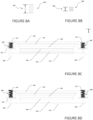
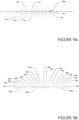
- a shape change of activate loading mechanism 106a is triggered.
- the shape change is caused by the shape memory material in activate loading mechanism 106a that changes shape at a specific temperature (a selectable property of shape memory material).
- the specific temperature that activates the shape memory material can be heat from heat source 104.
- FIGURE 6B is a simplified block diagram of active loading mechanism 106j coupled to heatsink 126b.
- active loading mechanism 106j and heatsink 126b can be positioned over heat source 104.
- Heat source 104 can be over substrate 130.
- Substrate 130 can be over PCB 132 and coupled to PCB 132 with solder balls 134.
- PCB 132 can include PCB attachment means 152.
- Attachment means 154 can be configured to be lowered over PCB attachment means 152, which similarly can consist of various geometries (e.g., ring, clip, posts, ledge, lip, arm, teeth, etc.).
- FIGURE 8D is a simplified block diagram of memory spring 160 being used in a shoulder screw and load frame thermal attached process.
- the shape memory material in memory spring 160 can be activated by the application of external heat or by the application of an electrical current and upon activation, memory spring 160 attempts to revert to its initial programmed shape height 162 (as illustrated in FIGURE 8A ). Because memory spring 160 is compressed between load frame 166 and shoulder screw head 176, the force of memory spring 160 attempting to revert to its initial programmed shape height 162 creates or increases an applied force from heatsink 126 onto TIM 128 and heat source 104.
Landscapes
- Engineering & Computer Science (AREA)
- Microelectronics & Electronic Packaging (AREA)
- Physics & Mathematics (AREA)
- Theoretical Computer Science (AREA)
- Human Computer Interaction (AREA)
- General Engineering & Computer Science (AREA)
- General Physics & Mathematics (AREA)
- Thermal Sciences (AREA)
- Cooling Or The Like Of Electrical Apparatus (AREA)
Claims (10)
- Elektronische Vorrichtung, umfassend:eine gedruckte Schaltplatine (132), wobei die gedruckte Schaltplatine (132) sichere Pfosten (136) einschließt;eine Wärmequelle (104), die sich auf der gedruckten Schaltplatine (132) befindet; undeinen aktiven Lastmechanismus (106), der an der gedruckten Schaltplatine (132) gesichert ist, festgehalten durch Befestigungen an den sicheren Pfosten (136),wobei der aktive Lastmechanismus (106) Fortsätze (122), einen Hauptkörper (124) und eine Wärmesenke (126) einschließt,wobei der Hauptkörper (124) über der Wärmesenke (126) ist, und die Wärmesenke (126) über der Wärmequelle (104) ist,wobei die Fortsätze (122) sich von dem Hauptkörper (124) zu den sicheren Pfosten (136) erstrecken, wobei die Fortsätze (122) aus Formgedächtnismaterial zusammengesetzt sind, undwobei der aktive Lastmechanismus (106) eine erste Last auf die Wärmequelle (104) anwendet, wenn das Formgedächtnismaterial nicht aktiviert wird, und eine zweite Last auf die Wärmequelle (104) anwendet, wenn das Formgedächtnismaterial aktiviert wird.
- Elektronische Vorrichtung nach Anspruch 1, des Weiteren umfassend:
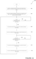
ein thermisches Schnittstellenmaterial (128) zwischen der Wärmequelle (104) und der Wärmesenke (126), wobei das thermische Schnittstellenmaterial (128) eine Dicke von etwa dreißig (30) Mikrometern hat. - Elektronische Vorrichtung nach einem der Ansprüche 1 bis 2, wobei der aktive Lastmechanismus (106) aktiviert wird, wenn eine Temperatur der Wärmequelle (104) einen Schwellenwert erfüllt.
- Elektronische Vorrichtung nach einem der Ansprüche 1 bis 3, wobei der aktive Lastmechanismus (106) durch Wärme von der Wärmequelle (104) aktiviert wird.
- Elektronische Vorrichtung nach einem der Ansprüche 1 bis 3, wobei der aktive Lastmechanismus (106) durch resistive Erwärmung von einem elektrischen Strom aktiviert wird.
- Elektronische Vorrichtung nach einem der Ansprüche 1 bis 5, wobei das Formgedächtnismaterial eine Nickel-Titan-Legierung ist.
- Verfahren, umfassend:Bestimmen, ob eine Temperatur einer Wärmequelle (104) einen Schwellenwert erfüllt, wobei die Wärmequelle (104) sich auf einer gedruckten Schaltplatine (132) befindet; undAktivieren eines aktiven Lastmechanismus (106), wenn die Temperatur der Wärmequelle (104) den Schwellenwert erfüllt, wobei der aktive Lastmechanismus (106) Fortsätze (122), einen Hauptkörper (124) und eine Wärmesenke (126) einschließt, wobei der Hauptkörper (124) über der Wärmesenke (126) ist und die Wärmesenke (126) über der Wärmequelle (104) ist, und der aktive Lastmechanismus (106) an der gedruckten Schaltplatine (132) gesichert ist, festgehalten durch Befestigung an sicheren Pfosten (136), die die gedruckte Schaltplatine (132) einschließt, wobei die Fortsätze (122) sich von dem Hauptkörper (124) zu den sicheren Pfosten (136) erstrecken, die Fortsätze (122) aus Formgedächtnismaterial zusammengesetzt sind, und wobei der aktive Lastmechanismus (106) eine erste Last auf die Wärmequelle (104) anwendet, wenn das Formgedächtnismaterial nicht aktiviert ist, und eine zweite Last auf die Wärmequelle (104) anwendet, wenn das Formgedächtnismaterial aktiviert ist.
- Verfahren nach Anspruch 7, wobei ein thermisches Schnittstellenmaterial (128) zwischen der Wärmequelle (104) und der Wärmesenke (126) ist und das thermische Schnittstellenmaterial (128) eine Dicke von etwa dreißig (30) Mikrometern hat.
- Verfahren nach einem der Ansprüche 7 und 8, des Weiteren umfassend:
Deaktivieren des aktiven Lastmechanismus (106), wenn die Temperatur der Wärmequelle (104) den Schwellenwert nicht erfüllt. - Verfahren nach einem der Ansprüche 7 bis 9, wobei der aktive Lastmechanismus (106) durch Wärme von der Wärmequelle (104) aktiviert wird.
Applications Claiming Priority (1)
| Application Number | Priority Date | Filing Date | Title |
|---|---|---|---|
| US16/370,506 US10880986B2 (en) | 2019-03-29 | 2019-03-29 | Activate loading mechanism |
Publications (2)
| Publication Number | Publication Date |
|---|---|
| EP3716745A1 EP3716745A1 (de) | 2020-09-30 |
| EP3716745B1 true EP3716745B1 (de) | 2023-07-05 |
Family
ID=67475883
Family Applications (1)
| Application Number | Title | Priority Date | Filing Date |
|---|---|---|---|
| EP20154196.8A Active EP3716745B1 (de) | 2019-03-29 | 2020-01-28 | Elektronische vorrichtung mit aktivierung von belastungsmechanismus und verfahren |
Country Status (3)
| Country | Link |
|---|---|
| US (1) | US10880986B2 (de) |
| EP (1) | EP3716745B1 (de) |
| CN (1) | CN111755398A (de) |
Families Citing this family (9)
| Publication number | Priority date | Publication date | Assignee | Title |
|---|---|---|---|---|
| US10939584B1 (en) * | 2019-08-22 | 2021-03-02 | Getac Technology Corporation | Heat dissipation module and assembly method thereof |
| DE102019132314B4 (de) * | 2019-11-28 | 2022-03-03 | Infineon Technologies Ag | Package mit Einkapselung unter Kompressionsbelastung |
| US11324110B2 (en) * | 2020-03-03 | 2022-05-03 | Honeywell International Inc. | Standoff for circuit board having temperature-variable electrical element |
| US11019751B2 (en) | 2020-03-27 | 2021-05-25 | Intel Corporation | Activate loading mechanism |
| US11589481B2 (en) | 2020-08-14 | 2023-02-21 | Cisco Technology, Inc. | Heat sink assembly for electronic equipment |
| US12114466B2 (en) * | 2020-12-23 | 2024-10-08 | Intel Corporation | Heat pipe with in-plane heat spreader and loading mechanism |
| CN114690335A (zh) * | 2020-12-29 | 2022-07-01 | 华为技术有限公司 | 光笼子组件、光模块连接器,及光笼子组件的制造方法 |
| US12146476B2 (en) * | 2021-12-23 | 2024-11-19 | Intel Corporation | Flexible vapor chamber with shape memory material |
| US12069794B2 (en) | 2022-07-06 | 2024-08-20 | Cisco Technology, Inc. | Dynamic control of heat sink pressure |
Family Cites Families (8)
| Publication number | Priority date | Publication date | Assignee | Title |
|---|---|---|---|---|
| FR2629153B1 (fr) | 1988-03-22 | 1990-05-04 | Bull Sa | Dispositif de fixation a pression de deux pieces l'une a l'autre |
| US6672892B2 (en) * | 2001-09-28 | 2004-01-06 | Intel Corporation | Package retention module coupled directly to a socket |
| US6668550B2 (en) * | 2001-11-26 | 2003-12-30 | Sony Corporation | Method and apparatus for converting dissipated heat to work energy |
| US7080989B2 (en) * | 2004-06-10 | 2006-07-25 | Sun Microsystems, Inc. | Memory metal springs for heatsink attachments |
| FR2880192B1 (fr) | 2004-12-23 | 2007-06-01 | Sagem | Systeme a deux etats pour la regulation thermique d'un dispositif electronique |
| US20100129648A1 (en) * | 2008-11-26 | 2010-05-27 | Jun Xu | Electronic packaging and heat sink bonding enhancements, methods of production and uses thereof |
| US10558266B2 (en) * | 2017-06-30 | 2020-02-11 | Microsoft Technology Licensing, Llc | Shape memory alloy actuated haptic feedback |
| US11019751B2 (en) | 2020-03-27 | 2021-05-25 | Intel Corporation | Activate loading mechanism |
-
2019
- 2019-03-29 US US16/370,506 patent/US10880986B2/en active Active
-
2020
- 2020-01-28 EP EP20154196.8A patent/EP3716745B1/de active Active
- 2020-02-28 CN CN202010126882.1A patent/CN111755398A/zh active Pending
Also Published As
| Publication number | Publication date |
|---|---|
| US20190246488A1 (en) | 2019-08-08 |
| EP3716745A1 (de) | 2020-09-30 |
| US10880986B2 (en) | 2020-12-29 |
| CN111755398A (zh) | 2020-10-09 |
Similar Documents
| Publication | Publication Date | Title |
|---|---|---|
| EP3716745A1 (de) | Aktivierung von belastungsmechanismus | |
| EP3886157B1 (de) | Aktiver belastungsmechanismus | |
| US11573055B2 (en) | Vapor chamber and means of attachment | |
| US11963335B2 (en) | Heatsink with a sandwich plate construction | |
| EP2738804B1 (de) | Flexible thermische Übertragungsstreifen | |
| US11251103B2 (en) | Segmented heatsink | |
| US12336145B2 (en) | Vapor chamber with ionized fluid | |
| EP3799116B1 (de) | Strahlungsabschirmung um eine komponente auf einem substrat | |
| US9772143B2 (en) | Thermal module | |
| US20250048596A1 (en) | System and method to help mitigate heat in an electronic device | |
| US12146476B2 (en) | Flexible vapor chamber with shape memory material | |
| EP4020123B1 (de) | Wärmerohr mit auf gleicher ebene integriertem wärmeverteiler und lademechanismus | |
| US11576282B2 (en) | Cold plate attachment with stabilizing arm | |
| US10937717B2 (en) | Heatsink secured to a heat source | |
| US12585315B2 (en) | Fan enclosure with adjustable side venting | |
| US20230108943A1 (en) | Power conversion apparatus | |
| US10963015B2 (en) | Hybrid keyboard | |
| US20220338340A1 (en) | Hook and loop attachment for radiation shield and heat sink | |
| CN111106073B (zh) | 一种功率半导体器件的低应力薄膜结构 | |
| KR20020031436A (ko) | 방열 효율을 향상시킨 히트 싱크의 구조와 제조방법 |
Legal Events
| Date | Code | Title | Description |
|---|---|---|---|
| PUAI | Public reference made under article 153(3) epc to a published international application that has entered the european phase |
Free format text: ORIGINAL CODE: 0009012 |
|
| STAA | Information on the status of an ep patent application or granted ep patent |
Free format text: STATUS: THE APPLICATION HAS BEEN PUBLISHED |
|
| AK | Designated contracting states |
Kind code of ref document: A1 Designated state(s): AL AT BE BG CH CY CZ DE DK EE ES FI FR GB GR HR HU IE IS IT LI LT LU LV MC MK MT NL NO PL PT RO RS SE SI SK SM TR |
|
| AX | Request for extension of the european patent |
Extension state: BA ME |
|
| STAA | Information on the status of an ep patent application or granted ep patent |
Free format text: STATUS: REQUEST FOR EXAMINATION WAS MADE |
|
| 17P | Request for examination filed |
Effective date: 20210302 |
|
| RBV | Designated contracting states (corrected) |
Designated state(s): AL AT BE BG CH CY CZ DE DK EE ES FI FR GB GR HR HU IE IS IT LI LT LU LV MC MK MT NL NO PL PT RO RS SE SI SK SM TR |
|
| STAA | Information on the status of an ep patent application or granted ep patent |
Free format text: STATUS: EXAMINATION IS IN PROGRESS |
|
| 17Q | First examination report despatched |
Effective date: 20221027 |
|
| GRAP | Despatch of communication of intention to grant a patent |
Free format text: ORIGINAL CODE: EPIDOSNIGR1 |
|
| STAA | Information on the status of an ep patent application or granted ep patent |
Free format text: STATUS: GRANT OF PATENT IS INTENDED |
|
| RIC1 | Information provided on ipc code assigned before grant |
Ipc: H01L 23/373 19900101ALN20230112BHEP Ipc: H05K 1/02 19680901ALN20230112BHEP Ipc: H01L 23/552 19900101ALN20230112BHEP Ipc: H01L 23/42 19740701ALN20230112BHEP Ipc: G06F 1/20 19900101ALI20230112BHEP Ipc: H01L 23/40 19740701ALI20230112BHEP Ipc: H05K 7/20 19680901AFI20230112BHEP |
|
| INTG | Intention to grant announced |
Effective date: 20230130 |
|
| GRAS | Grant fee paid |
Free format text: ORIGINAL CODE: EPIDOSNIGR3 |
|
| GRAA | (expected) grant |
Free format text: ORIGINAL CODE: 0009210 |
|
| STAA | Information on the status of an ep patent application or granted ep patent |
Free format text: STATUS: THE PATENT HAS BEEN GRANTED |
|
| AK | Designated contracting states |
Kind code of ref document: B1 Designated state(s): AL AT BE BG CH CY CZ DE DK EE ES FI FR GB GR HR HU IE IS IT LI LT LU LV MC MK MT NL NO PL PT RO RS SE SI SK SM TR |
|
| REG | Reference to a national code |
Ref country code: CH Ref legal event code: EP |
|
| REG | Reference to a national code |
Ref country code: AT Ref legal event code: REF Ref document number: 1586031 Country of ref document: AT Kind code of ref document: T Effective date: 20230715 |
|
| REG | Reference to a national code |
Ref country code: DE Ref legal event code: R096 Ref document number: 602020013158 Country of ref document: DE |
|
| REG | Reference to a national code |
Ref country code: IE Ref legal event code: FG4D |
|
| P01 | Opt-out of the competence of the unified patent court (upc) registered |
Effective date: 20230707 |
|
| REG | Reference to a national code |
Ref country code: NL Ref legal event code: FP |
|
| REG | Reference to a national code |
Ref country code: LT Ref legal event code: MG9D |
|
| REG | Reference to a national code |
Ref country code: AT Ref legal event code: MK05 Ref document number: 1586031 Country of ref document: AT Kind code of ref document: T Effective date: 20230705 |
|
| PG25 | Lapsed in a contracting state [announced via postgrant information from national office to epo] |
Ref country code: GR Free format text: LAPSE BECAUSE OF FAILURE TO SUBMIT A TRANSLATION OF THE DESCRIPTION OR TO PAY THE FEE WITHIN THE PRESCRIBED TIME-LIMIT Effective date: 20231006 |
|
| PG25 | Lapsed in a contracting state [announced via postgrant information from national office to epo] |
Ref country code: ES Free format text: LAPSE BECAUSE OF FAILURE TO SUBMIT A TRANSLATION OF THE DESCRIPTION OR TO PAY THE FEE WITHIN THE PRESCRIBED TIME-LIMIT Effective date: 20230705 |
|
| PG25 | Lapsed in a contracting state [announced via postgrant information from national office to epo] |
Ref country code: IS Free format text: LAPSE BECAUSE OF FAILURE TO SUBMIT A TRANSLATION OF THE DESCRIPTION OR TO PAY THE FEE WITHIN THE PRESCRIBED TIME-LIMIT Effective date: 20231105 |
|
| PG25 | Lapsed in a contracting state [announced via postgrant information from national office to epo] |
Ref country code: SE Free format text: LAPSE BECAUSE OF FAILURE TO SUBMIT A TRANSLATION OF THE DESCRIPTION OR TO PAY THE FEE WITHIN THE PRESCRIBED TIME-LIMIT Effective date: 20230705 Ref country code: RS Free format text: LAPSE BECAUSE OF FAILURE TO SUBMIT A TRANSLATION OF THE DESCRIPTION OR TO PAY THE FEE WITHIN THE PRESCRIBED TIME-LIMIT Effective date: 20230705 Ref country code: PT Free format text: LAPSE BECAUSE OF FAILURE TO SUBMIT A TRANSLATION OF THE DESCRIPTION OR TO PAY THE FEE WITHIN THE PRESCRIBED TIME-LIMIT Effective date: 20231106 Ref country code: NO Free format text: LAPSE BECAUSE OF FAILURE TO SUBMIT A TRANSLATION OF THE DESCRIPTION OR TO PAY THE FEE WITHIN THE PRESCRIBED TIME-LIMIT Effective date: 20231005 Ref country code: LV Free format text: LAPSE BECAUSE OF FAILURE TO SUBMIT A TRANSLATION OF THE DESCRIPTION OR TO PAY THE FEE WITHIN THE PRESCRIBED TIME-LIMIT Effective date: 20230705 Ref country code: LT Free format text: LAPSE BECAUSE OF FAILURE TO SUBMIT A TRANSLATION OF THE DESCRIPTION OR TO PAY THE FEE WITHIN THE PRESCRIBED TIME-LIMIT Effective date: 20230705 Ref country code: IS Free format text: LAPSE BECAUSE OF FAILURE TO SUBMIT A TRANSLATION OF THE DESCRIPTION OR TO PAY THE FEE WITHIN THE PRESCRIBED TIME-LIMIT Effective date: 20231105 Ref country code: HR Free format text: LAPSE BECAUSE OF FAILURE TO SUBMIT A TRANSLATION OF THE DESCRIPTION OR TO PAY THE FEE WITHIN THE PRESCRIBED TIME-LIMIT Effective date: 20230705 Ref country code: GR Free format text: LAPSE BECAUSE OF FAILURE TO SUBMIT A TRANSLATION OF THE DESCRIPTION OR TO PAY THE FEE WITHIN THE PRESCRIBED TIME-LIMIT Effective date: 20231006 Ref country code: FI Free format text: LAPSE BECAUSE OF FAILURE TO SUBMIT A TRANSLATION OF THE DESCRIPTION OR TO PAY THE FEE WITHIN THE PRESCRIBED TIME-LIMIT Effective date: 20230705 Ref country code: ES Free format text: LAPSE BECAUSE OF FAILURE TO SUBMIT A TRANSLATION OF THE DESCRIPTION OR TO PAY THE FEE WITHIN THE PRESCRIBED TIME-LIMIT Effective date: 20230705 Ref country code: AT Free format text: LAPSE BECAUSE OF FAILURE TO SUBMIT A TRANSLATION OF THE DESCRIPTION OR TO PAY THE FEE WITHIN THE PRESCRIBED TIME-LIMIT Effective date: 20230705 |
|
| PG25 | Lapsed in a contracting state [announced via postgrant information from national office to epo] |
Ref country code: PL Free format text: LAPSE BECAUSE OF FAILURE TO SUBMIT A TRANSLATION OF THE DESCRIPTION OR TO PAY THE FEE WITHIN THE PRESCRIBED TIME-LIMIT Effective date: 20230705 |
|
| REG | Reference to a national code |
Ref country code: DE Ref legal event code: R097 Ref document number: 602020013158 Country of ref document: DE |
|
| PG25 | Lapsed in a contracting state [announced via postgrant information from national office to epo] |
Ref country code: SM Free format text: LAPSE BECAUSE OF FAILURE TO SUBMIT A TRANSLATION OF THE DESCRIPTION OR TO PAY THE FEE WITHIN THE PRESCRIBED TIME-LIMIT Effective date: 20230705 Ref country code: RO Free format text: LAPSE BECAUSE OF FAILURE TO SUBMIT A TRANSLATION OF THE DESCRIPTION OR TO PAY THE FEE WITHIN THE PRESCRIBED TIME-LIMIT Effective date: 20230705 Ref country code: EE Free format text: LAPSE BECAUSE OF FAILURE TO SUBMIT A TRANSLATION OF THE DESCRIPTION OR TO PAY THE FEE WITHIN THE PRESCRIBED TIME-LIMIT Effective date: 20230705 Ref country code: DK Free format text: LAPSE BECAUSE OF FAILURE TO SUBMIT A TRANSLATION OF THE DESCRIPTION OR TO PAY THE FEE WITHIN THE PRESCRIBED TIME-LIMIT Effective date: 20230705 Ref country code: CZ Free format text: LAPSE BECAUSE OF FAILURE TO SUBMIT A TRANSLATION OF THE DESCRIPTION OR TO PAY THE FEE WITHIN THE PRESCRIBED TIME-LIMIT Effective date: 20230705 Ref country code: SK Free format text: LAPSE BECAUSE OF FAILURE TO SUBMIT A TRANSLATION OF THE DESCRIPTION OR TO PAY THE FEE WITHIN THE PRESCRIBED TIME-LIMIT Effective date: 20230705 |
|
| PLBE | No opposition filed within time limit |
Free format text: ORIGINAL CODE: 0009261 |
|
| STAA | Information on the status of an ep patent application or granted ep patent |
Free format text: STATUS: NO OPPOSITION FILED WITHIN TIME LIMIT |
|
| PG25 | Lapsed in a contracting state [announced via postgrant information from national office to epo] |
Ref country code: IT Free format text: LAPSE BECAUSE OF FAILURE TO SUBMIT A TRANSLATION OF THE DESCRIPTION OR TO PAY THE FEE WITHIN THE PRESCRIBED TIME-LIMIT Effective date: 20230705 |
|
| 26N | No opposition filed |
Effective date: 20240408 |
|
| PG25 | Lapsed in a contracting state [announced via postgrant information from national office to epo] |
Ref country code: SI Free format text: LAPSE BECAUSE OF FAILURE TO SUBMIT A TRANSLATION OF THE DESCRIPTION OR TO PAY THE FEE WITHIN THE PRESCRIBED TIME-LIMIT Effective date: 20230705 |
|
| PG25 | Lapsed in a contracting state [announced via postgrant information from national office to epo] |
Ref country code: MC Free format text: LAPSE BECAUSE OF FAILURE TO SUBMIT A TRANSLATION OF THE DESCRIPTION OR TO PAY THE FEE WITHIN THE PRESCRIBED TIME-LIMIT Effective date: 20230705 |
|
| PG25 | Lapsed in a contracting state [announced via postgrant information from national office to epo] |
Ref country code: MC Free format text: LAPSE BECAUSE OF FAILURE TO SUBMIT A TRANSLATION OF THE DESCRIPTION OR TO PAY THE FEE WITHIN THE PRESCRIBED TIME-LIMIT Effective date: 20230705 |
|
| REG | Reference to a national code |
Ref country code: CH Ref legal event code: PL |
|
| PG25 | Lapsed in a contracting state [announced via postgrant information from national office to epo] |
Ref country code: LU Free format text: LAPSE BECAUSE OF NON-PAYMENT OF DUE FEES Effective date: 20240128 |
|
| PG25 | Lapsed in a contracting state [announced via postgrant information from national office to epo] |
Ref country code: LU Free format text: LAPSE BECAUSE OF NON-PAYMENT OF DUE FEES Effective date: 20240128 |
|
| PG25 | Lapsed in a contracting state [announced via postgrant information from national office to epo] |
Ref country code: BE Free format text: LAPSE BECAUSE OF NON-PAYMENT OF DUE FEES Effective date: 20240131 |
|
| PG25 | Lapsed in a contracting state [announced via postgrant information from national office to epo] |
Ref country code: CH Free format text: LAPSE BECAUSE OF NON-PAYMENT OF DUE FEES Effective date: 20240131 |
|
| PG25 | Lapsed in a contracting state [announced via postgrant information from national office to epo] |
Ref country code: CH Free format text: LAPSE BECAUSE OF NON-PAYMENT OF DUE FEES Effective date: 20240131 Ref country code: BE Free format text: LAPSE BECAUSE OF NON-PAYMENT OF DUE FEES Effective date: 20240131 |
|
| REG | Reference to a national code |
Ref country code: BE Ref legal event code: MM Effective date: 20240131 |
|
| PG25 | Lapsed in a contracting state [announced via postgrant information from national office to epo] |
Ref country code: BG Free format text: LAPSE BECAUSE OF FAILURE TO SUBMIT A TRANSLATION OF THE DESCRIPTION OR TO PAY THE FEE WITHIN THE PRESCRIBED TIME-LIMIT Effective date: 20230705 |
|
| PG25 | Lapsed in a contracting state [announced via postgrant information from national office to epo] |
Ref country code: BG Free format text: LAPSE BECAUSE OF FAILURE TO SUBMIT A TRANSLATION OF THE DESCRIPTION OR TO PAY THE FEE WITHIN THE PRESCRIBED TIME-LIMIT Effective date: 20230705 |
|
| PGFP | Annual fee paid to national office [announced via postgrant information from national office to epo] |
Ref country code: NL Payment date: 20241230 Year of fee payment: 6 |
|
| PGFP | Annual fee paid to national office [announced via postgrant information from national office to epo] |
Ref country code: GB Payment date: 20241219 Year of fee payment: 6 |
|
| PGFP | Annual fee paid to national office [announced via postgrant information from national office to epo] |
Ref country code: FR Payment date: 20241223 Year of fee payment: 6 |
|
| PG25 | Lapsed in a contracting state [announced via postgrant information from national office to epo] |
Ref country code: IE Free format text: LAPSE BECAUSE OF NON-PAYMENT OF DUE FEES Effective date: 20240128 |
|
| PG25 | Lapsed in a contracting state [announced via postgrant information from national office to epo] |
Ref country code: IE Free format text: LAPSE BECAUSE OF NON-PAYMENT OF DUE FEES Effective date: 20240128 |
|
| PG25 | Lapsed in a contracting state [announced via postgrant information from national office to epo] |
Ref country code: CY Free format text: LAPSE BECAUSE OF FAILURE TO SUBMIT A TRANSLATION OF THE DESCRIPTION OR TO PAY THE FEE WITHIN THE PRESCRIBED TIME-LIMIT; INVALID AB INITIO Effective date: 20200128 |
|
| PG25 | Lapsed in a contracting state [announced via postgrant information from national office to epo] |
Ref country code: HU Free format text: LAPSE BECAUSE OF FAILURE TO SUBMIT A TRANSLATION OF THE DESCRIPTION OR TO PAY THE FEE WITHIN THE PRESCRIBED TIME-LIMIT; INVALID AB INITIO Effective date: 20200128 |
|
| PG25 | Lapsed in a contracting state [announced via postgrant information from national office to epo] |
Ref country code: TR Free format text: LAPSE BECAUSE OF FAILURE TO SUBMIT A TRANSLATION OF THE DESCRIPTION OR TO PAY THE FEE WITHIN THE PRESCRIBED TIME-LIMIT Effective date: 20230705 |
|
| PGFP | Annual fee paid to national office [announced via postgrant information from national office to epo] |
Ref country code: DE Payment date: 20251216 Year of fee payment: 7 |