EP3716740A1 - Conformal coating blockage by surface-mount technology solder features - Google Patents
Conformal coating blockage by surface-mount technology solder features Download PDFInfo
- Publication number
- EP3716740A1 EP3716740A1 EP20162987.0A EP20162987A EP3716740A1 EP 3716740 A1 EP3716740 A1 EP 3716740A1 EP 20162987 A EP20162987 A EP 20162987A EP 3716740 A1 EP3716740 A1 EP 3716740A1
- Authority
- EP
- European Patent Office
- Prior art keywords
- integrated circuit
- circuit board
- printed circuit
- pcb
- conformal coating
- Prior art date
- Legal status (The legal status is an assumption and is not a legal conclusion. Google has not performed a legal analysis and makes no representation as to the accuracy of the status listed.)
- Granted
Links
Images


Classifications
-
- H—ELECTRICITY
- H05—ELECTRIC TECHNIQUES NOT OTHERWISE PROVIDED FOR
- H05K—PRINTED CIRCUITS; CASINGS OR CONSTRUCTIONAL DETAILS OF ELECTRIC APPARATUS; MANUFACTURE OF ASSEMBLAGES OF ELECTRICAL COMPONENTS
- H05K3/00—Apparatus or processes for manufacturing printed circuits
- H05K3/30—Assembling printed circuits with electric components, e.g. with resistors
- H05K3/32—Assembling printed circuits with electric components, e.g. with resistors electrically connecting electric components or wires to printed circuits
- H05K3/34—Assembling printed circuits with electric components, e.g. with resistors electrically connecting electric components or wires to printed circuits by soldering
- H05K3/341—Surface mounted components
- H05K3/3431—Leadless components
- H05K3/3436—Leadless components having an array of bottom contacts, e.g. pad grid array or ball grid array components
-
- B—PERFORMING OPERATIONS; TRANSPORTING
- B23—MACHINE TOOLS; METAL-WORKING NOT OTHERWISE PROVIDED FOR
- B23K—SOLDERING OR UNSOLDERING; WELDING; CLADDING OR PLATING BY SOLDERING OR WELDING; CUTTING BY APPLYING HEAT LOCALLY, e.g. FLAME CUTTING; WORKING BY LASER BEAM
- B23K1/00—Soldering, e.g. brazing, or unsoldering
- B23K1/0008—Soldering, e.g. brazing, or unsoldering specially adapted for particular articles or work
-
- H—ELECTRICITY
- H05—ELECTRIC TECHNIQUES NOT OTHERWISE PROVIDED FOR
- H05K—PRINTED CIRCUITS; CASINGS OR CONSTRUCTIONAL DETAILS OF ELECTRIC APPARATUS; MANUFACTURE OF ASSEMBLAGES OF ELECTRICAL COMPONENTS
- H05K1/00—Printed circuits
- H05K1/18—Printed circuits structurally associated with non-printed electric components
- H05K1/181—Printed circuits structurally associated with non-printed electric components associated with surface mounted components
-
- H—ELECTRICITY
- H05—ELECTRIC TECHNIQUES NOT OTHERWISE PROVIDED FOR
- H05K—PRINTED CIRCUITS; CASINGS OR CONSTRUCTIONAL DETAILS OF ELECTRIC APPARATUS; MANUFACTURE OF ASSEMBLAGES OF ELECTRICAL COMPONENTS
- H05K3/00—Apparatus or processes for manufacturing printed circuits
- H05K3/22—Secondary treatment of printed circuits
- H05K3/28—Applying non-metallic protective coatings
-
- H—ELECTRICITY
- H05—ELECTRIC TECHNIQUES NOT OTHERWISE PROVIDED FOR
- H05K—PRINTED CIRCUITS; CASINGS OR CONSTRUCTIONAL DETAILS OF ELECTRIC APPARATUS; MANUFACTURE OF ASSEMBLAGES OF ELECTRICAL COMPONENTS
- H05K3/00—Apparatus or processes for manufacturing printed circuits
- H05K3/22—Secondary treatment of printed circuits
- H05K3/28—Applying non-metallic protective coatings
- H05K3/284—Applying non-metallic protective coatings for encapsulating mounted components
-
- H—ELECTRICITY
- H05—ELECTRIC TECHNIQUES NOT OTHERWISE PROVIDED FOR
- H05K—PRINTED CIRCUITS; CASINGS OR CONSTRUCTIONAL DETAILS OF ELECTRIC APPARATUS; MANUFACTURE OF ASSEMBLAGES OF ELECTRICAL COMPONENTS
- H05K3/00—Apparatus or processes for manufacturing printed circuits
- H05K3/30—Assembling printed circuits with electric components, e.g. with resistors
- H05K3/32—Assembling printed circuits with electric components, e.g. with resistors electrically connecting electric components or wires to printed circuits
- H05K3/34—Assembling printed circuits with electric components, e.g. with resistors electrically connecting electric components or wires to printed circuits by soldering
- H05K3/3452—Solder masks
-
- B—PERFORMING OPERATIONS; TRANSPORTING
- B23—MACHINE TOOLS; METAL-WORKING NOT OTHERWISE PROVIDED FOR
- B23K—SOLDERING OR UNSOLDERING; WELDING; CLADDING OR PLATING BY SOLDERING OR WELDING; CUTTING BY APPLYING HEAT LOCALLY, e.g. FLAME CUTTING; WORKING BY LASER BEAM
- B23K2101/00—Articles made by soldering, welding or cutting
- B23K2101/36—Electric or electronic devices
- B23K2101/42—Printed circuits
-
- H—ELECTRICITY
- H05—ELECTRIC TECHNIQUES NOT OTHERWISE PROVIDED FOR
- H05K—PRINTED CIRCUITS; CASINGS OR CONSTRUCTIONAL DETAILS OF ELECTRIC APPARATUS; MANUFACTURE OF ASSEMBLAGES OF ELECTRICAL COMPONENTS
- H05K2201/00—Indexing scheme relating to printed circuits covered by H05K1/00
- H05K2201/09—Shape and layout
- H05K2201/09818—Shape or layout details not covered by a single group of H05K2201/09009 - H05K2201/09809
- H05K2201/09872—Insulating conformal coating
-
- H—ELECTRICITY
- H05—ELECTRIC TECHNIQUES NOT OTHERWISE PROVIDED FOR
- H05K—PRINTED CIRCUITS; CASINGS OR CONSTRUCTIONAL DETAILS OF ELECTRIC APPARATUS; MANUFACTURE OF ASSEMBLAGES OF ELECTRICAL COMPONENTS
- H05K2201/00—Indexing scheme relating to printed circuits covered by H05K1/00
- H05K2201/09—Shape and layout
- H05K2201/09818—Shape or layout details not covered by a single group of H05K2201/09009 - H05K2201/09809
- H05K2201/09909—Special local insulating pattern, e.g. as dam around component
-
- H—ELECTRICITY
- H05—ELECTRIC TECHNIQUES NOT OTHERWISE PROVIDED FOR
- H05K—PRINTED CIRCUITS; CASINGS OR CONSTRUCTIONAL DETAILS OF ELECTRIC APPARATUS; MANUFACTURE OF ASSEMBLAGES OF ELECTRICAL COMPONENTS
- H05K2201/00—Indexing scheme relating to printed circuits covered by H05K1/00
- H05K2201/10—Details of components or other objects attached to or integrated in a printed circuit board
- H05K2201/10613—Details of electrical connections of non-printed components, e.g. special leads
- H05K2201/10621—Components characterised by their electrical contacts
- H05K2201/10636—Leadless chip, e.g. chip capacitor or resistor
-
- H—ELECTRICITY
- H05—ELECTRIC TECHNIQUES NOT OTHERWISE PROVIDED FOR
- H05K—PRINTED CIRCUITS; CASINGS OR CONSTRUCTIONAL DETAILS OF ELECTRIC APPARATUS; MANUFACTURE OF ASSEMBLAGES OF ELECTRICAL COMPONENTS
- H05K2201/00—Indexing scheme relating to printed circuits covered by H05K1/00
- H05K2201/10—Details of components or other objects attached to or integrated in a printed circuit board
- H05K2201/10613—Details of electrical connections of non-printed components, e.g. special leads
- H05K2201/10621—Components characterised by their electrical contacts
- H05K2201/10727—Leadless chip carrier [LCC], e.g. chip-modules for cards
-
- Y—GENERAL TAGGING OF NEW TECHNOLOGICAL DEVELOPMENTS; GENERAL TAGGING OF CROSS-SECTIONAL TECHNOLOGIES SPANNING OVER SEVERAL SECTIONS OF THE IPC; TECHNICAL SUBJECTS COVERED BY FORMER USPC CROSS-REFERENCE ART COLLECTIONS [XRACs] AND DIGESTS
- Y02—TECHNOLOGIES OR APPLICATIONS FOR MITIGATION OR ADAPTATION AGAINST CLIMATE CHANGE
- Y02P—CLIMATE CHANGE MITIGATION TECHNOLOGIES IN THE PRODUCTION OR PROCESSING OF GOODS
- Y02P70/00—Climate change mitigation technologies in the production process for final industrial or consumer products
- Y02P70/50—Manufacturing or production processes characterised by the final manufactured product
Definitions
- This disclosure relates to printed circuit boards, and in particular, to systems and methods for blocking conformal coating using surface-mount technology solder features.
- Surface-mount devices such as integrated circuits (IC) (e.g., analog signal ICs, digital signal ICs, or mixed signal ICs), typically comprise a set of electronic components, such as transistors or other suitable components, inseparably integrated on a relatively small portion of semiconductor material (e.g., silicon or other suitable material).
- IC integrated circuits
- Modern ICs may integrate millions or billions of electronic components and may be used in various applications, such as desktop computers, laptop computers, mobile computing devices, tablet computing devices, home appliances, stereos, medical devices, and a plurality of other electronic devices.
- an IC is typically connected, using surface-mount technology (SMT) (e.g., solder or other thermally conductive material applied to conductive pads disposed on a side of the IC facing the printed circuit board), to a printed circuit board (PCB) substrate, which electrically connects other ICs and electronic components on the PCB.
- SMT surface-mount technology
- PCB printed circuit board
- solder and flux e.g., a paste that promotes solder flow
- PCB e.g., typically referred to as a PCB assembly (PCBA) when the ICs and electronic components are secured and electrically connected to the PCB.
- PCBA PCB assembly
- a conformal coating material is applied to the PCB after the IC and/or other electronic components are soldered to the PCB.
- the conformal coating material typically includes polymers and other suitable material.
- the conformal coating material when applied to the PCB, typically forms a thin layer that protects components of the PCB from moisture, dust, chemicals, and/or surface electrical changes.
- some of the conforming coating material may flow between the IC, or other electronic components, and the PCB. This may cause accelerated solder fatigue to solder connections that connect the IC, or other electronic components, to the PCB.
- This disclosure relates generally to conformal coating control systems and methods.
- An aspect of the disclosed embodiments is a conformal coating control method.
- the method includes arranging at least one conformal control surface feature on a surface of a printed circuit board proximate perimeter pads of an integrated circuit.
- the method also includes soldering, to the printed circuit board, the integrated circuit.
- the method also includes applying a conformal coating material to the printed circuit board, wherein the conformal coating material is at least partially restricted from flowing between the integrated circuit and the printed circuit board by solder flux residue accumulated proximate the conformal control surface feature.
- the at least one conformal control surface feature may include a solder mask material.
- the perimeter pads of the integrated circuit may define channels between the integrated circuit and the printed circuit board.
- the solder mask material may partially fill at least some of the channels defined by the perimeter pads of the integrated circuit.
- the solder mask material may partially fill each of the channels defined by the perimeter pads of the integrated circuit.
- the at least one conformal control surface feature may include at least one solderable member arranged proximate the perimeter pads of the printed circuit board and proximate a corner of the integrated circuit.
- the at least one solderable member may include a 90 degree angle bracket.
- the integrated circuit may include a quad-flat no-leads package.
- the system includes a printed circuit board and an integrated circuit disposed on a surface of the printed circuit board, wherein a solder mask material is disposed on the surface of the printed circuit board proximate perimeter pads of the integrated circuit.
- the system also includes at least one solderable member disposed on the printed circuit board proximate the integrated circuit.
- the system also includes a conformal coating material that is applied to the printed circuit board, wherein the conformal coating material is at least partially restricted from flowing between the integrated circuit and the printed circuit board by solder flux residue accumulated proximate of the solder mask material and the at least one solderable member.
- the solder mask material may reduce a stand-off gap height between the integrated circuit and the printed circuit board.
- the perimeter pads of the integrated circuit may define channels between the integrated circuit and the printed circuit board.
- solder mask material may partially fill at least some of the channels defined by the perimeter pads of the integrated circuit.
- the solder mask material may partially fill each of the channels defined by the perimeter pads of the integrated circuit.
- the at least one solderable member may be arranged proximate a corner of the integrated circuit.
- the at least one solderable member may include a 90 degree angle bracket.
- the integrated circuit may include a quad-flat no-leads package.
- the method includes applying a solder mask material into channels on a printed circuit board defined by an integrated circuit.
- the method also includes arranging, on the printed circuit board and proximate a corner of the integrated circuit, a solderable member.
- the method also includes soldering, to the printed circuit board, the integrated circuit, wherein soldering the integrated circuit to the printed circuit board causes solder flux residue to accumulate proximate the solder mask material and the solderable member.
- the method also includes applying a conformal coating material to the printed circuit board, wherein the conformal coating material is at least partially restricted, by the solder flux residue, from flowing between the integrated circuit and the printed circuit board.
- the solder mask material may reduce a stand-off gap height between the integrated circuit and the printed circuit board.
- the solderable member may include a 90 degree angle bracket.
- the integrated circuit may include a quad-flat no-leads device.
- IC integrated circuits
- ICs typically comprise a set of electronic components, such as transistors or other suitable components, inseparably integrated on a relatively small portion of semiconductor material (e.g., silicon or other suitable material).
- ICs may include microprocessors, microcontrollers, memory chips, application-specific integrated circuits (ASICs), field-programmable gate arrays (FPGAs), sensors, power management circuits, operation amplifiers, analog-to-digital converters, digital-to-analog converters, and the like.
- the ICs may include a flat no-leads package, such as a quad-flat no-leads package, a dual-flat no-leads package, or other suitable no-leads package.
- Modern ICs may integrate millions or billions of electronic components and may be used in various applications, such as desktop computers, laptop computers, mobile computing devices, tablet computing devices, home appliances, stereos, medical devices, and a plurality of other electronic devices.
- An IC is typically connected, using surface-mount technology (e.g., solder or other thermally conductive material applied to conductive pads disposed on a side of the IC facing the printed circuit board), to the printed circuit board (PCB) substrate, which electrically connects other ICs and electronic components (e.g., resistors, capacitors, indictors, transformers, power resistors, large area passives, and the like) the PCB.
- PCB printed circuit board
- one or more leads of the IC may be soldered to the substrate to electrically connect the IC to the other ICs and electronic components on the PCB and/or to one another.
- solder such as a lead alloy solder or other suitable solder
- the solder provides a conductive path for electrons to flow to and from the IC via the substrate.
- solder and flux e.g., a paste that promotes solder flow
- PCB assembly PCBA
- a conformal coating material is applied to the PCB after the IC and/or other electronic components are soldered to the PCB.
- the conformal coating material typically includes acrylic material, epoxy material, polyurethane material, silicone material, fluorinated poly-para-xylylene material, non-fluorinated poly-para-xylylene material, amorphous fluoropolymer material, or other suitable material.
- the conformal coating material may be applied to the PCB by brushing the conformal coating material onto the PCB, by spraying the conformal coating material onto the PCB, by dispensing the conformal coating material onto the PCB, by dipping the PCB in the conformal coating material, or by other suitable application processes.
- the conformal coating material when applied to the PCB, typically forms a thin layer (e.g., 25 micrometers to 250 micrometers) that conforms to contours of the PCB.
- the conformal coating material protects components (e.g., such as ICs and other electronic components) of the PCB from moisture, dust, chemicals, and/or surface electrical changes.
- some of the conforming coating material may flow between the IC, or other electronic components, and the PCB.
- a stand-off gap may be defined between a surface of the IC facing the PCB and the PCB.
- the conformal coating material may flow into the stand-off gap during application of the conforming coating material to the PCB. This may cause accelerated solder fatigue to solder connections that connect the IC, or other electronic components, to the PCB. Accordingly, systems and methods, such as those described herein, that control the flow of conformal coating material during the application of the conformal coating material to the PCB, may be desirable.
- the system and methods disclosed herein include may include using surface features on the PCB that cause solder paste flux residue to accumulate proximate the IC and/or other electronic components.
- the solder paste flux residue may restrict the flow of conformal coating material from flowing between the IC and/or other electronic components, during application of the conformal coating material to the PCB.
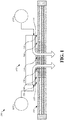
- FIG. 1 generally illustrates a printed circuit board assembly (PCBA) 100 according to the principles of the present disclosure.
- the PCBA 100 may be used in any suitable application, such as a desktop computer, a laptop computer, a mobile computing device, a tablet computing device, a home appliance, a stereo, a medical device, or any other suitable electrical device. Additionally, or alternatively, the PCBA 100 may interact with a plurality of other PCBAs.
- the PCBA 100 includes an integrated circuit (IC) 102 and a printed circuit board (PCB) 104.
- the IC 102 may include a plurality of electronic components inseparably integrated and/or disposed on a segment of semiconductor material, such as silicon or other suitable semiconductor material.
- the IC 102 may comprise a microprocessor, a microcontroller, a memory chip, an application-specific integrated circuit (ASIC), a field-programmable gate array (FPGA), a sensor, a power management circuit, an operation amplifier, an analog-to-digital converter, a digital-to-analog converter, or other suitable IC. Additionally, or alternatively, the IC 102 may comprise an analog signal IC, a digital signal IC, or a mixed signal IC.
- the IC 102 may include a flat no-leads package, such as a quad-flat no-leads package, a dual-flat no-leads package, or other suitable no-leads package.
- the IC 102 may include a 5 millimeter by 5 millimeter quad-flat no-leads package, a 9 millimeter by 9 millimeter quad-flat no-leads package, 10 millimeter by 10 millimeter quad-flat no-leads package, or other suitable quad-flat no-leads package.
- the IC 102 may include an exposed pad disposed on a bottom surface of the IC 102 (e.g., a surface that faces the PCB 104).
- the exposed pad may include a plurality of leads adapted to be electrically connected to the PCB 104.
- thermal conductive material such as solder, may be applied between a respective lead and a portion of a substrate on the PCB 104.
- the PCBA 100 may include one or more power resistors, one or more large area passives, other suitable electronic components, or a combination thereof.
- the PCB 104 may be adapted to mechanically support the IC 102 and/or other ICs and electronic components, and to electrically connect such components.
- the PCB 104 may include, as described, substrates, pads, and other features that may be etched into one or more layers of conductive material, such as copper or other suitable conductive material.
- the layers of conductive material of the PCB 104 may be laminated onto or sandwiched between layers of non-conductive material.
- the PCBA 100 includes one or more stand-off gaps 106.
- the stand-off gaps 106 may be defined by a surface of the IC 102 that faces the PCB 104 and a surface of the PCB 104 that faces the IC 102.
- the PCBA 100 may include one or more power sources 110.
- the power sources 110 may include current sources, voltage sources, or other suitable power source.
- the power sources 110 may include a power circuit comprising a voltage source, one or more resistors, one or more capacitors, and/or one or more other suitable electronic components.
- the PCBA 100 includes a high side power source 110 and a low side power source 110, however, the PCBA 100 may omit either of the high side power source 110 or the low side power source 110.
- power e.g., voltage and/or current
- the power flows through the components of the IC 102 and into the substrate of the PCB 104 via the solder connections between the IC 102 and the substrate of the PCB 104.
- the PCBA 100 may include additional or few components than illustrated and/or described herein.
- the PCBA 100 may include a pedestal (e.g., a heat sink) and a PCBA case or housing.
- the PCBA housing may be configured to house or enclose the IC 102, PCB 104, and/or the pedestal.
- the pedestal may be disposed on a side of the PCB 104 opposite the IC 102.
- the PCB 104 may be attached to the pedestal using a suitable thermal interface material (e.g., thermal glue or other thermally conductive material).
- the pedestal may include a heat sink configured to draw heat generated by the IC 102 away from the IC 102.
- a conformal coating material may be applied to the PCB 104 after the IC 102 and/or other electronic components are connected to the PCB 104 using solder or other suitable thermal conductive material.
- the conformal coating material includes acrylic material, epoxy material, polyurethane material, silicone material, fluorinated poly-para-xylylene material, non-fluorinated poly-para-xylylene material, amorphous fluoropolymer material, or other suitable material.
- the conformal coating material may be applied to the PCB 104 by brushing the conformal coating material onto the PCB 104, by spraying the conformal coating material onto the PCB 104, by dispensing the conformal coating material onto the PCB 104, by dipping the PCB 104 in the conformal coating material, or by other suitable application processes.
- the conformal coating material when applied to the PCB 104, forms a thin layer (e.g., 25 micrometers to 250 micrometers) that conforms to contours of the PCB 104.
- the conformal coating material protects the IC 102 and/or other electronic components connected of the PCB 104 from moisture, dust, chemicals, other contaminants, changes in temperature, and the like.
- the PCB 104 may include one or more conformal control surface features configured to restrict or control flow of the conformal coating material proximate the IC 102 and/or other electronic components.
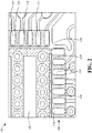
- FIG. 2 generally illustrates a cutaway top view of a printed circuit board (PCB) 104 according to the principles of the present disclosure.
- the IC 102 may be connected, via solder or other suitable thermal conductive material, to the PCB 104. It should be understood that, while only IC 102 is described as being connected to the PCB 104, additional ICs and/or other electronic components may be connected to the PCB 104. Accordingly, the principles of the present disclosure described herein apply to any suitable electronic component connected to the PCB 104.
- the IC 102 may include exposed pad 112 disposed on the surface of the IC 102 facing the PCB 104 adapted to be connected, via solder or other thermal conductive material, to a corresponding pad or a portion of a substrate on the PCB 104.
- the IC 102 includes a plurality of perimeter pads 114 disposed along a perimeter of the IC 102.
- the perimeter pads 114 are adapted to be connected, via solder or other thermal conductive material, to corresponding pads or corresponding portions of the substrate of the PCB 104.
- the perimeter pads 114 may include any suitable dimensions.
- a perimeter pad 114 may include a 0.25 millimeter width and a 0.69 millimeter length, 0.20 millimeter width and a 0.73 millimeter length, or any suitable dimensions.
- the perimeter pads 114 define channels 116 between the IC 102 and the PCB 104.
- the channels 116 may include any suitable dimensions.
- the channels 116 may include a 0.25 millimeter width, 0.30 millimeter width, or any other suitable dimension.
- the exposed pad 112 and/or the perimeter pads 114 define the stand-off gap 106 between the IC 102 and the PCB 104.
- the IC 102 includes one or more corners 118 (e.g., four corners or any suitable number of corners corresponding to a shape of the IC 102), as is illustrated in FIG. 1 .
- Each respective corner 118 of the IC 102 are proximate a corresponding gap 120.
- the gap 120 may be defined by the surface of the IC 102 facing the PCB 104, the PCB 104, and one or more perimeter pads 114 proximate the respective corner 118 corresponding to the gap 120.
- the conformal coating material may flow into the channels 116 and/or one or more gaps 120.
- the portion of conformal coating material may fill or partially fill the stand-off gap 106, the channels 116, and/or the gaps 120. This may accelerate solder fatigue of the solder connections between the IC 102 and the PCB 104 (e.g., due to physical expansion of the solder during thermal cycling).
- the PCB 104 may include one or more surface features as is generally illustrated in FIG. 3 .
- the surface features may include a solder mask material 122.
- the solder mask material 122 may include a thin lacquer-like layer of polymer or other suitable material.
- the solder mask material 122 may be applied to all or substantially of respective gaps between respective pads on the PCB 104 corresponding to the perimeter pads 114 (e.g., before the IC 102 is brought into contact with the PCB 104 to define the channels 116). Additionally, or alternatively, the solder mask material 122 may be applied to a portion of the surface of the PCB 104 corresponding to respective gaps 120.
- the solder mask material 122 may fill or substantially fill each respective channel 116 and/or each respective gap 120, as is generally illustrated in FIG. 3 .
- the solder mask material 122 by filling or substantially filling each respective channel 116 and/or each respective gap 120 may reduce the stand-off gap 106 between the IC 102 and the PCB 104 (e.g., by filling or substantially filling space within the stand-off gap 106).
- solder is then applied to the PCB 104 and the IC 102 in order to electrically connect the IC 102 to the PCB 104.
- solder flux residue accumulates proximate the solder mask material 122 that is applied to the PCB 104.
- the conformal coating material is then applied to the PCB 104 and the IC 102.
- the solder flux residue accumulated proximate the solder mask material 122 blocks the flow of conformal coating material and prevents, at least some, of the conformal coating material from flowing into the channels 116 and/or the gaps 120.
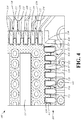
- the solder mask material 122 may be applied a portion of the respective gaps between respective pads on the PCB 104 corresponding to the perimeter pads 114 (e.g., before the IC 102 is brought into contact with the PCB 104 to define the channels 116). Additionally, or alternatively, the solder mask material 122 may be applied to a portion of the surface of the PCB 104 corresponding to respective gaps 120. When the IC 102 is seated onto the PCB 104, the solder mask material 122 may partially fill each respective channel 116 and/or each respective gap 120, as is generally illustrated in FIG. 4 .
- the solder mask material 122 by filling or substantially filling each respective channel 116 and/or each respective gap 120, may reduce the stand-off gap 106 between the IC 102 and the PCB 104 (e.g., by filling or substantially filling space within the stand-off gap 106).
- solder flux residue accumulates proximate the solder mask material 122 that is applied to the PCB 104.
- the conformal coating material is then applied to the PCB 104 and the IC 102.
- the solder flux residue accumulated proximate the solder mask material 122 partially blocks the flow of conformal coating material and prevents, at least some, of the conformal coating material from flowing into the channels 116 and/or the gaps 120, while allowing, at least some, of the conformal coating material to flow into a portion of the channels 116 and/or the gaps 120 not blocked by the solder flux residue.
- the solder mask material 122 may fill or substantially fill some of the channels 116 and may partially fill others of the channels 116. In some embodiments, the solder mask material 122 may fill or substantially fill some of the channels 116 and not others of the channels 116. In some embodiments, the solder mask material 122 may partially fill some of the channels 116 and not others of the channels 116.
- the surface features may include a solderable member 124 attached to the surface of the PCB 104.
- the solderable member 124 may include a solderable land and may comprise any suitable material, such as copper, zinc, brass, or other suitable solderable material.
- the solderable member 124 may include a straight member, a curved member, an angled member, or other suitable solderable member.
- the solderable member 124 may include an angled bracket such as a 90° or substantially 90°-angled bracket, or other suitable angled bracket.
- one or more solderable members 124 may be disposed on the surface of the PCB 104 proximate respective corners 118 of the IC 102.
- solderable members 124 may be attached to portions of the PCB 104 (e.g., before the IC 102 is brought into contact with the PCB 104, defining the gaps 120) corresponding to respective corners 118 of the IC 102.
- the PCB 104 may include one solderable member 124, two solderable members 124, three solderable members 124, four solderable members 124, or any suitable number of solderable members 124.
- the PCB 104 may include one or more solderable members 124 disposed proximate any other portion of the IC 102 other than the corners 118 and/or a combination of other portions of the IC 102 and one or more of the corners 118 of the IC 102.
- solder flux residue accumulates proximate the solderable members 124 disposed on the PCB 104.
- the conformal coating material is then applied to the PCB 104 and the IC 102.
- the solder flux residue accumulated proximate the solderable members 124 blocks the flow of conformal coating material and prevents, at least some, of the conformal coating material from flowing into the respective gaps 120 (e.g., gaps 120 corresponding to solderable members 124 disposed on the PCB 104).
- the PCB 104 may include a combination of solder mask material 122 and one or more solderable members 124.
- solder flux residue accumulates proximate the solder mask material 122 applied to the PCB 104 and proximate solderable members 124 disposed on the PCB 104.
- the conformal coating material is then applied to the PCB 104 and the IC 102.
- solder flux residue accumulated proximate the solder mask material 122 and the solderable members 124 blocks the flow of conformal coating material and prevents, at least some, of the conformal coating material from flowing into the channels 116 having solder mask material 122 partially or substantially filled with solder mask material 122 and the gaps 120 corresponding the solderable members 124 disposed on the PCB 104.
- the PCB 104 may include any combination of any amount of solder mask material 122 and any number of solder members 124.
- FIG. 5 is a flow diagram generally illustrating a conformal coating control method 200 according to the principles of the present disclosure.
- the method 200 arranges at least one conformal control surface feature on a printed circuit board.
- the conformal control surface feature may include solder mask material 122 (e.g., applied to various portions of the PCB 104 corresponding to perimeter pads 114 of the IC 102 and/or respective gaps 120) one or more solder members 124, or a combination thereof.
- the solder mask material 122 may partially fill or substantially fill the all of the channels 116, partially fill some of the channels 116 and substantially fill others of the channels 116, partially fill some of the channels 116 and not fill others of the channels 116, substantially fill some of the channels 116 and not fill others of the channels 116, or any combination thereof.
- the PCB 104 may include any suitable number of solderable members 124 disposed proximate respective corners 118 of the IC 102 and/or proximate other suitable portions of the IC 102.
- the PCB 104 includes any suitable combination of solder mask material 122 and solderable members 124.
- the method 200 solders an integrated circuit to the printed circuit board.
- the IC 102 is soldered to the PCB 104.
- solder residue flux accumulates proximate the conformal control surface features applied to the PCB 104.
- the method 200 applies conformal coating material to the printed circuit board.
- conformal coating material is applied to the IC 102 and the PCB 104.
- the solder flux residue accumulated proximate the conformal control surface features at least partially blocks or controls the flow of conformal coating material, such that the conformal coating material is restricted from flowing into the channels 116 and/or the gaps 120.
- a conformal coating control method includes arranging at least one conformal control surface feature on a surface of a printed circuit board proximate perimeter pads of an integrated circuit. The method also includes soldering, to the printed circuit board, the integrated circuit. The method also includes applying a conformal coating material to the printed circuit board, wherein the conformal coating material is at least partially restricted from flowing between the integrated circuit and the printed circuit board by solder flux residue accumulated proximate the conformal control surface feature.
- the at least one conformal control surface feature includes a solder mask material.
- the perimeter pads of the integrated circuit define channels between the integrated circuit and the printed circuit board.
- the solder mask material partially fills at least some of the channels defined by the perimeter pads of the integrated circuit.
- the solder mask material partially fills each of the channels defined by the perimeter pads of the integrated circuit.
- the at least one conformal control surface feature includes at least one solderable member arranged proximate the perimeter pads of the printed circuit board and proximate a corner of the integrated circuit.
- the at least one solderable member includes a 90 degree angle bracket.
- the integrated circuit includes a quad-flat no-leads package.
- a system for conformal coating control includes a printed circuit board and an integrated circuit disposed on a surface of the printed circuit board, wherein a solder mask material is disposed on the surface of the printed circuit board proximate perimeter pads of the integrated circuit.
- the system also includes at least one solderable member disposed on the printed circuit board proximate the integrated circuit.
- the system also includes a conformal coating material that is applied to the printed circuit board, wherein the conformal coating material is at least partially restricted from flowing between the integrated circuit and the printed circuit board by solder flux residue accumulated proximate of the solder mask material and the at least one solderable member.
- the solder mask material reduces a stand-off gap height between the integrated circuit and the printed circuit board.
- the perimeter pads of the integrated circuit define channels between the integrated circuit and the printed circuit board.
- the solder mask material partially fills at least some of the channels defined by the perimeter pads of the integrated circuit.
- the solder mask material partially fills each of the channels defined by the perimeter pads of the integrated circuit.
- the at least one solderable member is arranged proximate a corner of the integrated circuit.
- the at least one solderable member includes a 90 degree angle bracket.
- the integrated circuit includes a quad-flat no-leads package.
- a conformal coating control method includes applying a solder mask material into channels on a printed circuit board defined by an integrated circuit. The method also includes arranging, on the printed circuit board and proximate a corner of the integrated circuit, a solderable member. The method also includes soldering, to the printed circuit board, the integrated circuit, wherein soldering the integrated circuit to the printed circuit board causes solder flux residue to accumulate proximate the solder mask material and the solderable member. The method also includes applying a conformal coating material to the printed circuit board, wherein the conformal coating material is at least partially restricted, by the solder flux residue, from flowing between the integrated circuit and the printed circuit board.
- the solder mask material reduces a stand-off gap height between the integrated circuit and the printed circuit board.
- the solderable member includes a 90 degree angle bracket.
- the integrated circuit includes a quad-flat no-leads device.
- example is used herein to mean serving as an example, instance, or illustration. Any aspect or design described herein as “example” is not necessarily to be construed as preferred or advantageous over other aspects or designs. Rather, use of the word “example” is intended to present concepts in a concrete fashion.
- the term “or” is intended to mean an inclusive “or” rather than an exclusive “or”. That is, unless specified otherwise, or clear from context, "X includes A or B” is intended to mean any of the natural inclusive permutations. That is, if X includes A; X includes B; or X includes both A and B, then "X includes A or B" is satisfied under any of the foregoing instances.
- Implementations the systems, algorithms, methods, instructions, etc., described herein can be realized in hardware, software, or any combination thereof.
- the hardware can include, for example, computers, intellectual property (IP) cores, application-specific integrated circuits (ASICs), programmable logic arrays, optical processors, programmable logic controllers, microcode, microcontrollers, servers, microprocessors, digital signal processors, or any other suitable circuit.
- IP intellectual property
- ASICs application-specific integrated circuits
- programmable logic arrays optical processors
- programmable logic controllers microcode, microcontrollers
- servers microprocessors, digital signal processors, or any other suitable circuit.
- signal processors digital signal processors, or any other suitable circuit.
- module can include a packaged functional hardware unit designed for use with other components, a set of instructions executable by a controller (e.g., a processor executing software or firmware), processing circuitry configured to perform a particular function, and a self-contained hardware or software component that interfaces with a larger system.
- a module can include an application specific integrated circuit (ASIC), a Field Programmable Gate Array (FPGA), a circuit, digital logic circuit, an analog circuit, a combination of discrete circuits, gates, and other types of hardware or combination thereof.
- a module can include memory that stores instructions executable by a controller to implement a feature of the module.
- systems described herein can be implemented using a general-purpose computer or general-purpose processor with a computer program that, when executed, carries out any of the respective methods, algorithms, and/or instructions described herein.
- a special purpose computer/processor can be utilized which can contain other hardware for carrying out any of the methods, algorithms, or instructions described herein.
- implementations of the present disclosure can take the form of a computer program product accessible from, for example, a computer-usable or computer-readable medium.
- a computer-usable or computer-readable medium can be any device that can, for example, tangibly contain, store, communicate, or transport the program for use by or in connection with any processor.
- the medium can be, for example, an electronic, magnetic, optical, electromagnetic, or a semiconductor device. Other suitable mediums are also available.
Landscapes
- Engineering & Computer Science (AREA)
- Microelectronics & Electronic Packaging (AREA)
- Manufacturing & Machinery (AREA)
- Mechanical Engineering (AREA)
- Electric Connection Of Electric Components To Printed Circuits (AREA)
- Non-Metallic Protective Coatings For Printed Circuits (AREA)
Abstract
Description
- This disclosure relates to printed circuit boards, and in particular, to systems and methods for blocking conformal coating using surface-mount technology solder features.
- Surface-mount devices, such as integrated circuits (IC) (e.g., analog signal ICs, digital signal ICs, or mixed signal ICs), typically comprise a set of electronic components, such as transistors or other suitable components, inseparably integrated on a relatively small portion of semiconductor material (e.g., silicon or other suitable material). Modern ICs may integrate millions or billions of electronic components and may be used in various applications, such as desktop computers, laptop computers, mobile computing devices, tablet computing devices, home appliances, stereos, medical devices, and a plurality of other electronic devices.
- In such applications, an IC is typically connected, using surface-mount technology (SMT) (e.g., solder or other thermally conductive material applied to conductive pads disposed on a side of the IC facing the printed circuit board), to a printed circuit board (PCB) substrate, which electrically connects other ICs and electronic components on the PCB. Typically, solder and flux (e.g., a paste that promotes solder flow) are applied to the PCB (e.g., using a printing process or other suitable manufacturing process) to secure and electrically connect the IC, and other electronic components, to the PCB (e.g., typically referred to as a PCB assembly (PCBA) when the ICs and electronic components are secured and electrically connected to the PCB).
- Typically, a conformal coating material is applied to the PCB after the IC and/or other electronic components are soldered to the PCB. The conformal coating material typically includes polymers and other suitable material. The conformal coating material, when applied to the PCB, typically forms a thin layer that protects components of the PCB from moisture, dust, chemicals, and/or surface electrical changes. However, during application of the conformal coating material (e.g., such as a low viscosity conformal coating material), some of the conforming coating material may flow between the IC, or other electronic components, and the PCB. This may cause accelerated solder fatigue to solder connections that connect the IC, or other electronic components, to the PCB.
- This disclosure relates generally to conformal coating control systems and methods.
- An aspect of the disclosed embodiments is a conformal coating control method. The method includes arranging at least one conformal control surface feature on a surface of a printed circuit board proximate perimeter pads of an integrated circuit. The method also includes soldering, to the printed circuit board, the integrated circuit. The method also includes applying a conformal coating material to the printed circuit board, wherein the conformal coating material is at least partially restricted from flowing between the integrated circuit and the printed circuit board by solder flux residue accumulated proximate the conformal control surface feature.
- In the method, the at least one conformal control surface feature may include a solder mask material.
- Also in the method, the perimeter pads of the integrated circuit may define channels between the integrated circuit and the printed circuit board.
- In the method, the solder mask material may partially fill at least some of the channels defined by the perimeter pads of the integrated circuit.
- Also in the method, the solder mask material may partially fill each of the channels defined by the perimeter pads of the integrated circuit.
- In the method, the at least one conformal control surface feature may include at least one solderable member arranged proximate the perimeter pads of the printed circuit board and proximate a corner of the integrated circuit.
- Additionally in the method, the at least one solderable member may include a 90 degree angle bracket.
- Within the method, the integrated circuit may include a quad-flat no-leads package.
- Another aspect of the disclosed embodiments is a system for conformal coating control. The system includes a printed circuit board and an integrated circuit disposed on a surface of the printed circuit board, wherein a solder mask material is disposed on the surface of the printed circuit board proximate perimeter pads of the integrated circuit. The system also includes at least one solderable member disposed on the printed circuit board proximate the integrated circuit. The system also includes a conformal coating material that is applied to the printed circuit board, wherein the conformal coating material is at least partially restricted from flowing between the integrated circuit and the printed circuit board by solder flux residue accumulated proximate of the solder mask material and the at least one solderable member.
- In the system, the solder mask material may reduce a stand-off gap height between the integrated circuit and the printed circuit board.
- Within the system, the perimeter pads of the integrated circuit may define channels between the integrated circuit and the printed circuit board.
- Also within the system, the solder mask material may partially fill at least some of the channels defined by the perimeter pads of the integrated circuit.
- In the system, the solder mask material may partially fill each of the channels defined by the perimeter pads of the integrated circuit.
- Additionally in the system, the at least one solderable member may be arranged proximate a corner of the integrated circuit.
- In the system, the at least one solderable member may include a 90 degree angle bracket.
- Also in the system, the integrated circuit may include a quad-flat no-leads package.
- Another aspect of the disclosed embodiments is a conformal coating control method. The method includes applying a solder mask material into channels on a printed circuit board defined by an integrated circuit. The method also includes arranging, on the printed circuit board and proximate a corner of the integrated circuit, a solderable member. The method also includes soldering, to the printed circuit board, the integrated circuit, wherein soldering the integrated circuit to the printed circuit board causes solder flux residue to accumulate proximate the solder mask material and the solderable member. The method also includes applying a conformal coating material to the printed circuit board, wherein the conformal coating material is at least partially restricted, by the solder flux residue, from flowing between the integrated circuit and the printed circuit board.
- In the method, the solder mask material may reduce a stand-off gap height between the integrated circuit and the printed circuit board.
- Also in the method, the solderable member may include a 90 degree angle bracket.
- Additionally in the method, the integrated circuit may include a quad-flat no-leads device.
- These and other aspects of the present disclosure are provided in the following detailed description of the embodiments, the appended claims, and the accompanying figures.
- The disclosure is best understood from the following detailed description when read in conjunction with the accompanying drawings. It is emphasized that, according to common practice, the various features of the drawings are not to-scale. On the contrary, the dimensions of the various features are arbitrarily expanded or reduced for clarity.
-
FIG. 1 generally illustrates a printed circuit board assembly according to the principles of the present disclosure. -
FIG. 2 generally illustrates a cutaway top view of a printed circuit board according to the principles of the present disclosure. -
FIG. 3 generally illustrates a cutaway top view of the printed circuit board ofFIG. 2 including at least one conformal coating control surface feature. -
FIG. 4 generally illustrates a cutaway top view of the printed circuit board ofFIG. 2 including at least one conformal coating control surface feature. -
FIG. 5 is a flow diagram generally illustrating a conformal coating control method according to the principles of the present disclosure. - The following discussion is directed to various embodiments of the invention. Although one or more of these embodiments may be preferred, the embodiments disclosed should not be interpreted, or otherwise used, as limiting the scope of the disclosure, including the claims. In addition, one skilled in the art will understand that the following description has broad application, and the discussion of any embodiment is meant only to be exemplary of that embodiment, and not intended to intimate that the scope of the disclosure, including the claims, is limited to that embodiment.
- As described, surface-mount devices, such as integrated circuits (IC) (e.g., analog signal ICs, digital signal ICs, or mixed signal ICs), typically comprise a set of electronic components, such as transistors or other suitable components, inseparably integrated on a relatively small portion of semiconductor material (e.g., silicon or other suitable material). ICs may include microprocessors, microcontrollers, memory chips, application-specific integrated circuits (ASICs), field-programmable gate arrays (FPGAs), sensors, power management circuits, operation amplifiers, analog-to-digital converters, digital-to-analog converters, and the like. In some embodiments, the ICs may include a flat no-leads package, such as a quad-flat no-leads package, a dual-flat no-leads package, or other suitable no-leads package. Modern ICs may integrate millions or billions of electronic components and may be used in various applications, such as desktop computers, laptop computers, mobile computing devices, tablet computing devices, home appliances, stereos, medical devices, and a plurality of other electronic devices.
- An IC is typically connected, using surface-mount technology (e.g., solder or other thermally conductive material applied to conductive pads disposed on a side of the IC facing the printed circuit board), to the printed circuit board (PCB) substrate, which electrically connects other ICs and electronic components (e.g., resistors, capacitors, indictors, transformers, power resistors, large area passives, and the like) the PCB. For example, one or more leads of the IC may be soldered to the substrate to electrically connect the IC to the other ICs and electronic components on the PCB and/or to one another. The solder, such as a lead alloy solder or other suitable solder, provides a conductive path for electrons to flow to and from the IC via the substrate. Typically, solder and flux (e.g., a paste that promotes solder flow) are applied to the PCB (e.g., using a dipping process or other suitable manufacturing process) to secure and electrically connect the IC, and other electronic components, to the PCB (e.g., typically referred to as a PCB assembly (PCBA) when the ICs and electronic components are secured and electrically connected to the PCB).
- Typically, a conformal coating material is applied to the PCB after the IC and/or other electronic components are soldered to the PCB. The conformal coating material typically includes acrylic material, epoxy material, polyurethane material, silicone material, fluorinated poly-para-xylylene material, non-fluorinated poly-para-xylylene material, amorphous fluoropolymer material, or other suitable material. The conformal coating material may be applied to the PCB by brushing the conformal coating material onto the PCB, by spraying the conformal coating material onto the PCB, by dispensing the conformal coating material onto the PCB, by dipping the PCB in the conformal coating material, or by other suitable application processes. The conformal coating material, when applied to the PCB, typically forms a thin layer (e.g., 25 micrometers to 250 micrometers) that conforms to contours of the PCB. The conformal coating material protects components (e.g., such as ICs and other electronic components) of the PCB from moisture, dust, chemicals, and/or surface electrical changes.
- However, during application of the conformal coating material, some of the conforming coating material may flow between the IC, or other electronic components, and the PCB. For example, a stand-off gap may be defined between a surface of the IC facing the PCB and the PCB. The conformal coating material may flow into the stand-off gap during application of the conforming coating material to the PCB. This may cause accelerated solder fatigue to solder connections that connect the IC, or other electronic components, to the PCB. Accordingly, systems and methods, such as those described herein, that control the flow of conformal coating material during the application of the conformal coating material to the PCB, may be desirable. In some embodiments, as will be described, the system and methods disclosed herein include may include using surface features on the PCB that cause solder paste flux residue to accumulate proximate the IC and/or other electronic components. The solder paste flux residue may restrict the flow of conformal coating material from flowing between the IC and/or other electronic components, during application of the conformal coating material to the PCB.
-
FIG. 1 generally illustrates a printed circuit board assembly (PCBA) 100 according to the principles of the present disclosure. ThePCBA 100 may be used in any suitable application, such as a desktop computer, a laptop computer, a mobile computing device, a tablet computing device, a home appliance, a stereo, a medical device, or any other suitable electrical device. Additionally, or alternatively, thePCBA 100 may interact with a plurality of other PCBAs. - The
PCBA 100 includes an integrated circuit (IC) 102 and a printed circuit board (PCB) 104. TheIC 102 may include a plurality of electronic components inseparably integrated and/or disposed on a segment of semiconductor material, such as silicon or other suitable semiconductor material. TheIC 102 may comprise a microprocessor, a microcontroller, a memory chip, an application-specific integrated circuit (ASIC), a field-programmable gate array (FPGA), a sensor, a power management circuit, an operation amplifier, an analog-to-digital converter, a digital-to-analog converter, or other suitable IC. Additionally, or alternatively, theIC 102 may comprise an analog signal IC, a digital signal IC, or a mixed signal IC. In some embodiments, theIC 102 may include a flat no-leads package, such as a quad-flat no-leads package, a dual-flat no-leads package, or other suitable no-leads package. In some embodiments, theIC 102 may include a 5 millimeter by 5 millimeter quad-flat no-leads package, a 9 millimeter by 9 millimeter quad-flat no-leads package, 10 millimeter by 10 millimeter quad-flat no-leads package, or other suitable quad-flat no-leads package. - The
IC 102 may include an exposed pad disposed on a bottom surface of the IC 102 (e.g., a surface that faces the PCB 104). The exposed pad may include a plurality of leads adapted to be electrically connected to thePCB 104. For example, thermal conductive material such as solder, may be applied between a respective lead and a portion of a substrate on thePCB 104. It should be understood that while only theIC 102 is described herein, the principles of the present disclosure apply to any number of ICs and any suitable electronic components. For example, while not illustrated, thePCBA 100 may include one or more power resistors, one or more large area passives, other suitable electronic components, or a combination thereof. - The
PCB 104 may be adapted to mechanically support theIC 102 and/or other ICs and electronic components, and to electrically connect such components. ThePCB 104 may include, as described, substrates, pads, and other features that may be etched into one or more layers of conductive material, such as copper or other suitable conductive material. The layers of conductive material of thePCB 104 may be laminated onto or sandwiched between layers of non-conductive material. - In some embodiments, the
PCBA 100 includes one or more stand-offgaps 106. The stand-offgaps 106 may be defined by a surface of theIC 102 that faces thePCB 104 and a surface of thePCB 104 that faces theIC 102. ThePCBA 100 may include one ormore power sources 110. Thepower sources 110 may include current sources, voltage sources, or other suitable power source. Thepower sources 110 may include a power circuit comprising a voltage source, one or more resistors, one or more capacitors, and/or one or more other suitable electronic components. In some embodiments, thePCBA 100 includes a highside power source 110 and a lowside power source 110, however, thePCBA 100 may omit either of the highside power source 110 or the lowside power source 110. When power (e.g., voltage and/or current) is supplied by one of thepower sources 110, the power flows through the components of theIC 102 and into the substrate of thePCB 104 via the solder connections between theIC 102 and the substrate of thePCB 104. - In some embodiments, the
PCBA 100 may include additional or few components than illustrated and/or described herein. For example, thePCBA 100 may include a pedestal (e.g., a heat sink) and a PCBA case or housing. The PCBA housing may be configured to house or enclose theIC 102,PCB 104, and/or the pedestal. The pedestal may be disposed on a side of thePCB 104 opposite theIC 102. ThePCB 104 may be attached to the pedestal using a suitable thermal interface material (e.g., thermal glue or other thermally conductive material). The pedestal may include a heat sink configured to draw heat generated by theIC 102 away from theIC 102. - A conformal coating material may be applied to the
PCB 104 after theIC 102 and/or other electronic components are connected to thePCB 104 using solder or other suitable thermal conductive material. The conformal coating material includes acrylic material, epoxy material, polyurethane material, silicone material, fluorinated poly-para-xylylene material, non-fluorinated poly-para-xylylene material, amorphous fluoropolymer material, or other suitable material. The conformal coating material may be applied to thePCB 104 by brushing the conformal coating material onto thePCB 104, by spraying the conformal coating material onto thePCB 104, by dispensing the conformal coating material onto thePCB 104, by dipping thePCB 104 in the conformal coating material, or by other suitable application processes. The conformal coating material, when applied to thePCB 104, forms a thin layer (e.g., 25 micrometers to 250 micrometers) that conforms to contours of thePCB 104. As described, the conformal coating material protects theIC 102 and/or other electronic components connected of thePCB 104 from moisture, dust, chemicals, other contaminants, changes in temperature, and the like. As will be described, thePCB 104 may include one or more conformal control surface features configured to restrict or control flow of the conformal coating material proximate theIC 102 and/or other electronic components. -
FIG. 2 generally illustrates a cutaway top view of a printed circuit board (PCB) 104 according to the principles of the present disclosure. TheIC 102 may be connected, via solder or other suitable thermal conductive material, to thePCB 104. It should be understood that, while onlyIC 102 is described as being connected to thePCB 104, additional ICs and/or other electronic components may be connected to thePCB 104. Accordingly, the principles of the present disclosure described herein apply to any suitable electronic component connected to thePCB 104. - The
IC 102 may include exposedpad 112 disposed on the surface of theIC 102 facing thePCB 104 adapted to be connected, via solder or other thermal conductive material, to a corresponding pad or a portion of a substrate on thePCB 104. In some embodiments, theIC 102 includes a plurality ofperimeter pads 114 disposed along a perimeter of theIC 102. Theperimeter pads 114 are adapted to be connected, via solder or other thermal conductive material, to corresponding pads or corresponding portions of the substrate of thePCB 104. Theperimeter pads 114 may include any suitable dimensions. For example, aperimeter pad 114 may include a 0.25 millimeter width and a 0.69 millimeter length, 0.20 millimeter width and a 0.73 millimeter length, or any suitable dimensions. - The
perimeter pads 114 definechannels 116 between theIC 102 and thePCB 104. Thechannels 116 may include any suitable dimensions. For example, thechannels 116 may include a 0.25 millimeter width, 0.30 millimeter width, or any other suitable dimension. As described, the exposedpad 112 and/or theperimeter pads 114 define the stand-offgap 106 between theIC 102 and thePCB 104. TheIC 102 includes one or more corners 118 (e.g., four corners or any suitable number of corners corresponding to a shape of the IC 102), as is illustrated inFIG. 1 . Eachrespective corner 118 of theIC 102 are proximate acorresponding gap 120. Thegap 120 may be defined by the surface of theIC 102 facing thePCB 104, thePCB 104, and one ormore perimeter pads 114 proximate therespective corner 118 corresponding to thegap 120. - During application of the conformal coating material, a portion of the conformal coating material may flow into the
channels 116 and/or one ormore gaps 120. The portion of conformal coating material may fill or partially fill the stand-offgap 106, thechannels 116, and/or thegaps 120. This may accelerate solder fatigue of the solder connections between theIC 102 and the PCB 104 (e.g., due to physical expansion of the solder during thermal cycling). In order to control the flow of the conformal coating material (e.g., restrict, at least partially, the flow of conformal coating material into the stand-offgap 106, thechannels 116, and/or the gaps 120) during application of the conformal coating material, thePCB 104 may include one or more surface features as is generally illustrated inFIG. 3 . - In some embodiments, the surface features may include a
solder mask material 122. Thesolder mask material 122 may include a thin lacquer-like layer of polymer or other suitable material. In some embodiments, thesolder mask material 122 may be applied to all or substantially of respective gaps between respective pads on thePCB 104 corresponding to the perimeter pads 114 (e.g., before theIC 102 is brought into contact with thePCB 104 to define the channels 116). Additionally, or alternatively, thesolder mask material 122 may be applied to a portion of the surface of thePCB 104 corresponding torespective gaps 120. When theIC 102 is seated onto the PCB 104 (e.g., brought into contact with the PCB 104), thesolder mask material 122 may fill or substantially fill eachrespective channel 116 and/or eachrespective gap 120, as is generally illustrated inFIG. 3 . Thesolder mask material 122, by filling or substantially filling eachrespective channel 116 and/or eachrespective gap 120 may reduce the stand-offgap 106 between theIC 102 and the PCB 104 (e.g., by filling or substantially filling space within the stand-off gap 106). - Solder is then applied to the
PCB 104 and theIC 102 in order to electrically connect theIC 102 to thePCB 104. When the solder is applied to thePCB 104, solder flux residue accumulates proximate thesolder mask material 122 that is applied to thePCB 104. The conformal coating material is then applied to thePCB 104 and theIC 102. The solder flux residue accumulated proximate thesolder mask material 122 blocks the flow of conformal coating material and prevents, at least some, of the conformal coating material from flowing into thechannels 116 and/or thegaps 120. - In some embodiments, the
solder mask material 122 may be applied a portion of the respective gaps between respective pads on thePCB 104 corresponding to the perimeter pads 114 (e.g., before theIC 102 is brought into contact with thePCB 104 to define the channels 116). Additionally, or alternatively, thesolder mask material 122 may be applied to a portion of the surface of thePCB 104 corresponding torespective gaps 120. When theIC 102 is seated onto thePCB 104, thesolder mask material 122 may partially fill eachrespective channel 116 and/or eachrespective gap 120, as is generally illustrated inFIG. 4 . Thesolder mask material 122, by filling or substantially filling eachrespective channel 116 and/or eachrespective gap 120, may reduce the stand-offgap 106 between theIC 102 and the PCB 104 (e.g., by filling or substantially filling space within the stand-off gap 106). - When the solder is applied to the
PCB 104, solder flux residue accumulates proximate thesolder mask material 122 that is applied to thePCB 104. The conformal coating material is then applied to thePCB 104 and theIC 102. The solder flux residue accumulated proximate thesolder mask material 122 partially blocks the flow of conformal coating material and prevents, at least some, of the conformal coating material from flowing into thechannels 116 and/or thegaps 120, while allowing, at least some, of the conformal coating material to flow into a portion of thechannels 116 and/or thegaps 120 not blocked by the solder flux residue. - In some embodiments, the
solder mask material 122 may fill or substantially fill some of thechannels 116 and may partially fill others of thechannels 116. In some embodiments, thesolder mask material 122 may fill or substantially fill some of thechannels 116 and not others of thechannels 116. In some embodiments, thesolder mask material 122 may partially fill some of thechannels 116 and not others of thechannels 116. - In some embodiments, as is generally illustrated in
FIGS. 3 and4 , the surface features may include asolderable member 124 attached to the surface of thePCB 104. Thesolderable member 124 may include a solderable land and may comprise any suitable material, such as copper, zinc, brass, or other suitable solderable material. Thesolderable member 124 may include a straight member, a curved member, an angled member, or other suitable solderable member. For example, thesolderable member 124 may include an angled bracket such as a 90° or substantially 90°-angled bracket, or other suitable angled bracket. - In some embodiments, one or more
solderable members 124 may be disposed on the surface of thePCB 104 proximaterespective corners 118 of theIC 102. For example,solderable members 124 may be attached to portions of the PCB 104 (e.g., before theIC 102 is brought into contact with thePCB 104, defining the gaps 120) corresponding torespective corners 118 of theIC 102. ThePCB 104 may include onesolderable member 124, twosolderable members 124, threesolderable members 124, foursolderable members 124, or any suitable number ofsolderable members 124. In some embodiments, thePCB 104 may include one or moresolderable members 124 disposed proximate any other portion of theIC 102 other than thecorners 118 and/or a combination of other portions of theIC 102 and one or more of thecorners 118 of theIC 102. - When the solder is applied to the
PCB 104, solder flux residue accumulates proximate thesolderable members 124 disposed on thePCB 104. The conformal coating material is then applied to thePCB 104 and theIC 102. The solder flux residue accumulated proximate thesolderable members 124 blocks the flow of conformal coating material and prevents, at least some, of the conformal coating material from flowing into the respective gaps 120 (e.g.,gaps 120 corresponding tosolderable members 124 disposed on the PCB 104). - In some embodiments, the
PCB 104 may include a combination ofsolder mask material 122 and one or moresolderable members 124. When the solder is applied to thePCB 104, solder flux residue accumulates proximate thesolder mask material 122 applied to thePCB 104 and proximatesolderable members 124 disposed on thePCB 104. The conformal coating material is then applied to thePCB 104 and theIC 102. The solder flux residue accumulated proximate thesolder mask material 122 and thesolderable members 124 blocks the flow of conformal coating material and prevents, at least some, of the conformal coating material from flowing into thechannels 116 havingsolder mask material 122 partially or substantially filled withsolder mask material 122 and thegaps 120 corresponding thesolderable members 124 disposed on thePCB 104. It should be understood that thePCB 104 may include any combination of any amount ofsolder mask material 122 and any number ofsolder members 124. -
FIG. 5 is a flow diagram generally illustrating a conformalcoating control method 200 according to the principles of the present disclosure. At 202, themethod 200 arranges at least one conformal control surface feature on a printed circuit board. As described, the conformal control surface feature may include solder mask material 122 (e.g., applied to various portions of thePCB 104 corresponding toperimeter pads 114 of theIC 102 and/or respective gaps 120) one ormore solder members 124, or a combination thereof. In some embodiments, thesolder mask material 122 may partially fill or substantially fill the all of thechannels 116, partially fill some of thechannels 116 and substantially fill others of thechannels 116, partially fill some of thechannels 116 and not fill others of thechannels 116, substantially fill some of thechannels 116 and not fill others of thechannels 116, or any combination thereof. In some embodiments, thePCB 104 may include any suitable number ofsolderable members 124 disposed proximaterespective corners 118 of theIC 102 and/or proximate other suitable portions of theIC 102. In some embodiments, thePCB 104 includes any suitable combination ofsolder mask material 122 andsolderable members 124. - At 204, the
method 200 solders an integrated circuit to the printed circuit board. As described, theIC 102 is soldered to thePCB 104. When theIC 102 is soldered to thePCB 104, solder residue flux accumulates proximate the conformal control surface features applied to thePCB 104. At 206, themethod 200 applies conformal coating material to the printed circuit board. As described, conformal coating material is applied to theIC 102 and thePCB 104. When the conformal coating material is applied to theIC 102 and thePCB 104, the solder flux residue accumulated proximate the conformal control surface features at least partially blocks or controls the flow of conformal coating material, such that the conformal coating material is restricted from flowing into thechannels 116 and/or thegaps 120. - In some embodiments, a conformal coating control method includes arranging at least one conformal control surface feature on a surface of a printed circuit board proximate perimeter pads of an integrated circuit. The method also includes soldering, to the printed circuit board, the integrated circuit. The method also includes applying a conformal coating material to the printed circuit board, wherein the conformal coating material is at least partially restricted from flowing between the integrated circuit and the printed circuit board by solder flux residue accumulated proximate the conformal control surface feature.
- In some embodiments, the at least one conformal control surface feature includes a solder mask material. In some embodiments, the perimeter pads of the integrated circuit define channels between the integrated circuit and the printed circuit board. In some embodiments, the solder mask material partially fills at least some of the channels defined by the perimeter pads of the integrated circuit. In some embodiments, the solder mask material partially fills each of the channels defined by the perimeter pads of the integrated circuit. In some embodiments, the at least one conformal control surface feature includes at least one solderable member arranged proximate the perimeter pads of the printed circuit board and proximate a corner of the integrated circuit. In some embodiments, the at least one solderable member includes a 90 degree angle bracket. In some embodiments, the integrated circuit includes a quad-flat no-leads package.
- In some embodiments, a system for conformal coating control includes a printed circuit board and an integrated circuit disposed on a surface of the printed circuit board, wherein a solder mask material is disposed on the surface of the printed circuit board proximate perimeter pads of the integrated circuit. The system also includes at least one solderable member disposed on the printed circuit board proximate the integrated circuit. The system also includes a conformal coating material that is applied to the printed circuit board, wherein the conformal coating material is at least partially restricted from flowing between the integrated circuit and the printed circuit board by solder flux residue accumulated proximate of the solder mask material and the at least one solderable member.
- In some embodiments, the solder mask material reduces a stand-off gap height between the integrated circuit and the printed circuit board. In some embodiments, the perimeter pads of the integrated circuit define channels between the integrated circuit and the printed circuit board. In some embodiments, the solder mask material partially fills at least some of the channels defined by the perimeter pads of the integrated circuit. In some embodiments, the solder mask material partially fills each of the channels defined by the perimeter pads of the integrated circuit. In some embodiments, the at least one solderable member is arranged proximate a corner of the integrated circuit. In some embodiments, the at least one solderable member includes a 90 degree angle bracket. In some embodiments, the integrated circuit includes a quad-flat no-leads package.
- In some embodiments, a conformal coating control method includes applying a solder mask material into channels on a printed circuit board defined by an integrated circuit. The method also includes arranging, on the printed circuit board and proximate a corner of the integrated circuit, a solderable member. The method also includes soldering, to the printed circuit board, the integrated circuit, wherein soldering the integrated circuit to the printed circuit board causes solder flux residue to accumulate proximate the solder mask material and the solderable member. The method also includes applying a conformal coating material to the printed circuit board, wherein the conformal coating material is at least partially restricted, by the solder flux residue, from flowing between the integrated circuit and the printed circuit board.
- In some embodiments, the solder mask material reduces a stand-off gap height between the integrated circuit and the printed circuit board. In some embodiments, the solderable member includes a 90 degree angle bracket. In some embodiments, the integrated circuit includes a quad-flat no-leads device.
- The above discussion is meant to be illustrative of the principles and various embodiments of the present invention. Numerous variations and modifications will become apparent to those skilled in the art once the above disclosure is fully appreciated. It is intended that the following claims be interpreted to embrace all such variations and modifications.
- The word "example" is used herein to mean serving as an example, instance, or illustration. Any aspect or design described herein as "example" is not necessarily to be construed as preferred or advantageous over other aspects or designs. Rather, use of the word "example" is intended to present concepts in a concrete fashion. As used in this application, the term "or" is intended to mean an inclusive "or" rather than an exclusive "or". That is, unless specified otherwise, or clear from context, "X includes A or B" is intended to mean any of the natural inclusive permutations. That is, if X includes A; X includes B; or X includes both A and B, then "X includes A or B" is satisfied under any of the foregoing instances. In addition, the articles "a" and "an" as used in this application and the appended claims should generally be construed to mean "one or more" unless specified otherwise or clear from context to be directed to a singular form. Moreover, use of the term "an implementation" or "one implementation" throughout is not intended to mean the same embodiment or implementation unless described as such.
- Implementations the systems, algorithms, methods, instructions, etc., described herein can be realized in hardware, software, or any combination thereof. The hardware can include, for example, computers, intellectual property (IP) cores, application-specific integrated circuits (ASICs), programmable logic arrays, optical processors, programmable logic controllers, microcode, microcontrollers, servers, microprocessors, digital signal processors, or any other suitable circuit. In the claims, the term "processor" should be understood as encompassing any of the foregoing hardware, either singly or in combination. The terms "signal" and "data" are used interchangeably.
- As used herein, the term module can include a packaged functional hardware unit designed for use with other components, a set of instructions executable by a controller (e.g., a processor executing software or firmware), processing circuitry configured to perform a particular function, and a self-contained hardware or software component that interfaces with a larger system. For example, a module can include an application specific integrated circuit (ASIC), a Field Programmable Gate Array (FPGA), a circuit, digital logic circuit, an analog circuit, a combination of discrete circuits, gates, and other types of hardware or combination thereof. In other embodiments, a module can include memory that stores instructions executable by a controller to implement a feature of the module.
- Further, in one aspect, for example, systems described herein can be implemented using a general-purpose computer or general-purpose processor with a computer program that, when executed, carries out any of the respective methods, algorithms, and/or instructions described herein. In addition, or alternatively, for example, a special purpose computer/processor can be utilized which can contain other hardware for carrying out any of the methods, algorithms, or instructions described herein.
- Further, all or a portion of implementations of the present disclosure can take the form of a computer program product accessible from, for example, a computer-usable or computer-readable medium. A computer-usable or computer-readable medium can be any device that can, for example, tangibly contain, store, communicate, or transport the program for use by or in connection with any processor. The medium can be, for example, an electronic, magnetic, optical, electromagnetic, or a semiconductor device. Other suitable mediums are also available.
- The above-described embodiments, implementations, and aspects have been described in order to allow easy understanding of the present invention and do not limit the present invention. On the contrary, the invention is intended to cover various modifications and equivalent arrangements included within the scope of the appended claims, which scope is to be accorded the broadest interpretation so as to encompass all such modifications and equivalent structure as is permitted under the law.
Claims (20)
- A conformal coating control method (200), comprising:arranging (202) at least one conformal control surface feature (122, 124) on a surface of a printed circuit board (104) proximate perimeter pads (114) of an integrated circuit (102);soldering (204), to the printed circuit board (104), the integrated circuit (102); andapplying (206) a conformal coating material to the printed circuit board (104), wherein the conformal coating material is at least partially restricted from flowing between the integrated circuit (102) and the printed circuit board (104) by solder flux residue accumulated proximate the conformal control surface feature (122, 124).
- The method (200) of claim 1, wherein the at least one conformal control surface feature (122, 124) includes a solder mask material (122).
- The method (200) of claim 2, wherein the perimeter pads (114) of the integrated circuit (102) define channels (116) between the integrated circuit (102) and the printed circuit board (104).
- The method (200) of claim 3, wherein the solder mask material (122) partially fills at least some of the channels (116) defined by the perimeter pads (114) of the integrated circuit (102).
- The method (200) of claim 3, wherein the solder mask material (122) partially fills each of the channels (116) defined by the perimeter pads (114) of the integrated circuit (102).
- The method (200) of claim 1, wherein the at least one conformal control surface feature includes at least one solderable member (124) arranged proximate the perimeter pads (114) of the printed circuit board (104) and proximate a corner (118) of the integrated circuit (102).
- The method (200) of claim 6, wherein the at least one solderable member (124) includes a 90 degree angle bracket.
- The method (200) of claim 1, wherein the integrated circuit (102) includes a quad-flat no-leads package.
- A system for conformal coating control, the system comprising:a printed circuit board (104);an integrated circuit (102) disposed on a surface of the printed circuit board (104), wherein a solder mask material (122) is disposed on the surface of the printed circuit board (104) proximate perimeter pads (114) of the integrated circuit (102);at least one solderable member (124) disposed on the printed circuit board (104) proximate the integrated circuit (102); anda conformal coating material that is applied to the printed circuit board (104), wherein the conformal coating material is at least partially restricted from flowing between the integrated circuit (102) and the printed circuit board (104) by solder flux residue accumulated proximate of the solder mask material (122) and the at least one solderable member (124).
- The system of claim 9, wherein the solder mask material (122) reduces a stand-off gap height between the integrated circuit (102) and the printed circuit board (104).
- The system of claim 9, wherein the perimeter pads (114) of the integrated circuit (102) define channels (116) between the integrated circuit (102) and the printed circuit board (104).
- The system of claim 11, wherein the solder mask material (122) partially fills at least some of the channels (116) defined by the perimeter pads (114) of the integrated circuit (102).
- The system of claim 11, wherein the solder mask material (122) partially fills each of the channels (116) defined by the perimeter pads (114) of the integrated circuit (102).
- The system of claim 9, wherein the at least one solderable member (124) is arranged proximate a corner (118) of the integrated circuit (102).
- The system of claim 9, wherein the at least one solderable member (124) includes a 90 degree angle bracket.
- The system of claim 9, wherein the integrated circuit (102) includes a quad-flat no-leads package.
- A conformal coating control method (200), comprising:applying a solder mask material (122) into channels (116) on a printed circuit board (104) defined by an integrated circuit (102);arranging (202), on the printed circuit board (104) and proximate a corner (118) of the integrated circuit (102), a solderable member (124);soldering (204), to the printed circuit board (104), the integrated circuit (102), wherein soldering the integrated circuit (102) to the printed circuit board (104) causes solder flux residue to accumulate proximate the solder mask material (122) and the solderable member (124); andapplying (206) a conformal coating material to the printed circuit board (104), wherein the conformal coating material is at least partially restricted, by the solder flux residue, from flowing between the integrated circuit (102) and the printed circuit board (104) .
- The method (200) of claim 17, wherein the solder mask material (122) reduces a stand-off gap height between the integrated circuit (102) and the printed circuit board (104) .
- The method (200) of claim 17, wherein the solderable member (124) includes a 90 degree angle bracket.
- The method (200) of claim 17, wherein the integrated circuit (102) includes a quad-flat no-leads device.
Applications Claiming Priority (1)
| Application Number | Priority Date | Filing Date | Title |
|---|---|---|---|
| US16/366,909 US12284769B2 (en) | 2019-03-27 | 2019-03-27 | Conformal coating blockage by surface-mount technology solder features |
Publications (3)
| Publication Number | Publication Date |
|---|---|
| EP3716740A1 true EP3716740A1 (en) | 2020-09-30 |
| EP3716740B1 EP3716740B1 (en) | 2024-12-04 |
| EP3716740B8 EP3716740B8 (en) | 2025-01-08 |
Family
ID=69844476
Family Applications (1)
| Application Number | Title | Priority Date | Filing Date |
|---|---|---|---|
| EP20162987.0A Active EP3716740B8 (en) | 2019-03-27 | 2020-03-13 | Conformal coating blockage by surface-mount technology solder features |
Country Status (2)
| Country | Link |
|---|---|
| US (1) | US12284769B2 (en) |
| EP (1) | EP3716740B8 (en) |
Citations (4)
| Publication number | Priority date | Publication date | Assignee | Title |
|---|---|---|---|---|
| US20050260844A1 (en) * | 2004-05-21 | 2005-11-24 | Min-Keun Kwak | Package with barrier wall and method for manufacturing the same |
| US20130107483A1 (en) * | 2011-10-31 | 2013-05-02 | Mediatek Singapore Pte. Ltd. | Printed circuit board and electronic apparatus thereof |
| JP2015103782A (en) * | 2013-11-28 | 2015-06-04 | 株式会社東芝 | Semiconductor device |
| US20180070456A1 (en) * | 2016-09-06 | 2018-03-08 | Intel Corporation | Conformal coating of integrated circuit packages |
Family Cites Families (32)
| Publication number | Priority date | Publication date | Assignee | Title |
|---|---|---|---|---|
| US5266349A (en) | 1991-02-25 | 1993-11-30 | Specialty Coating Systems Inc. | Method of discrete conformal coating |
| JP2795788B2 (en) * | 1993-02-18 | 1998-09-10 | シャープ株式会社 | Semiconductor chip mounting method |
| US5704116A (en) * | 1996-05-03 | 1998-01-06 | Motorola, Inc. | Method of holding a component using an anhydride fluxing agent |
| US5985043A (en) * | 1997-07-21 | 1999-11-16 | Miguel Albert Capote | Polymerizable fluxing agents and fluxing adhesive compositions therefrom |
| US5796590A (en) * | 1996-11-05 | 1998-08-18 | Micron Electronics, Inc. | Assembly aid for mounting packaged integrated circuit devices to printed circuit boards |
| US6059172A (en) * | 1997-06-25 | 2000-05-09 | International Business Machines Corporation | Method for establishing electrical communication between a first object having a solder ball and a second object |
| KR100225655B1 (en) * | 1997-10-23 | 1999-10-15 | 윤종용 | Structure for mounting semiconductor ic on pcb |
| US6316736B1 (en) * | 1998-06-08 | 2001-11-13 | Visteon Global Technologies, Inc. | Anti-bridging solder ball collection zones |
| US6461881B1 (en) * | 2000-06-08 | 2002-10-08 | Micron Technology, Inc. | Stereolithographic method and apparatus for fabricating spacers for semiconductor devices and resulting structures |
| JP2003298220A (en) * | 2002-03-29 | 2003-10-17 | Hitachi Ltd | Circuit board, electronic device, and manufacturing method thereof |
| US6824041B2 (en) * | 2002-10-21 | 2004-11-30 | Agilent Technologies, Inc. | High temperature eutectic solder ball attach |
| US7028867B2 (en) | 2003-10-30 | 2006-04-18 | Nordson Corporation | Conformal coating applicator and method |
| JP2006303173A (en) * | 2005-04-20 | 2006-11-02 | Mitsubishi Electric Corp | Circuit board device and manufacturing method thereof |
| JP4251458B2 (en) * | 2005-12-21 | 2009-04-08 | Tdk株式会社 | Chip component mounting method and circuit board |
| JP2008210993A (en) * | 2007-02-26 | 2008-09-11 | Nec Corp | Printed wiring board and method of manufacturing the same |
| US20080216704A1 (en) | 2007-03-09 | 2008-09-11 | Fisher Controls International Llc | Conformal Coating |
| JP5510795B2 (en) * | 2008-01-30 | 2014-06-04 | 日本電気株式会社 | Electronic component mounting structure, electronic component mounting method, and electronic component mounting substrate |
| US8319114B2 (en) * | 2008-04-02 | 2012-11-27 | Densel Lambda K.K. | Surface mount power module dual footprint |
| TWI523127B (en) * | 2008-10-27 | 2016-02-21 | 松下知識產權經營股份有限公司 | Electronic device manufacturing method |
| CN102204420B (en) * | 2008-11-06 | 2013-11-13 | 住友电木株式会社 | Method for manufacturing electronic device and electronic device |
| US9770786B2 (en) * | 2010-06-01 | 2017-09-26 | Senju Metal Industry Co., Ltd. | Lead-free solder paste |
| JP5645592B2 (en) * | 2010-10-21 | 2014-12-24 | ルネサスエレクトロニクス株式会社 | Manufacturing method of semiconductor device |
| US9441119B2 (en) | 2011-03-28 | 2016-09-13 | Intermolecular, Inc. | Sol-gel transition control of coatings by addition of solidifiers for conformal coatings on textured glass |
| JP5218686B2 (en) * | 2011-08-08 | 2013-06-26 | Jsr株式会社 | Flux composition, method of forming electrical connection structure, electrical connection structure, and semiconductor device |
| US20130133193A1 (en) * | 2011-11-28 | 2013-05-30 | Mediatek Singapore Pte. Ltd. | Surface mount technology process for advanced quad flat no-lead package process and stencil used therewith |
| JP6586957B2 (en) * | 2014-09-19 | 2019-10-09 | ソニー株式会社 | Mounting board manufacturing method |
| AT516750B1 (en) * | 2014-12-18 | 2016-08-15 | Zizala Lichtsysteme Gmbh | Method for void reduction in solder joints |
| US10229901B2 (en) * | 2016-06-27 | 2019-03-12 | Taiwan Semiconductor Manufacturing Company, Ltd. | Immersion interconnections for semiconductor devices and methods of manufacture thereof |
| US20180332699A1 (en) * | 2017-02-21 | 2018-11-15 | Unlimiter Mfa Co., Ltd. | Printed circuit board |
| US10643938B2 (en) * | 2017-05-31 | 2020-05-05 | Intel Corporation | Standoff spacers for managing bondline thickness in microelectronic packages |
| WO2020026959A1 (en) * | 2018-07-31 | 2020-02-06 | 株式会社村田製作所 | Resin substrate, and method for manufacturing resin substrate |
| JP7142604B2 (en) * | 2019-05-15 | 2022-09-27 | 日本特殊陶業株式会社 | Wiring board and its manufacturing method |
-
2019
- 2019-03-27 US US16/366,909 patent/US12284769B2/en active Active
-
2020
- 2020-03-13 EP EP20162987.0A patent/EP3716740B8/en active Active
Patent Citations (4)
| Publication number | Priority date | Publication date | Assignee | Title |
|---|---|---|---|---|
| US20050260844A1 (en) * | 2004-05-21 | 2005-11-24 | Min-Keun Kwak | Package with barrier wall and method for manufacturing the same |
| US20130107483A1 (en) * | 2011-10-31 | 2013-05-02 | Mediatek Singapore Pte. Ltd. | Printed circuit board and electronic apparatus thereof |
| JP2015103782A (en) * | 2013-11-28 | 2015-06-04 | 株式会社東芝 | Semiconductor device |
| US20180070456A1 (en) * | 2016-09-06 | 2018-03-08 | Intel Corporation | Conformal coating of integrated circuit packages |
Also Published As
| Publication number | Publication date |
|---|---|
| US12284769B2 (en) | 2025-04-22 |
| US20200315030A1 (en) | 2020-10-01 |
| EP3716740B8 (en) | 2025-01-08 |
| EP3716740B1 (en) | 2024-12-04 |
Similar Documents
| Publication | Publication Date | Title |
|---|---|---|
| US20140029201A1 (en) | Power package module and manufacturing method thereof | |
| US10117322B2 (en) | Circuit assembly and electric junction box | |
| US8009429B1 (en) | Electrical component thermal management | |
| KR20090034889A (en) | Chip module for complete power train | |
| CN111668173A (en) | Electronic device module and method of manufacturing the same | |
| JP2015082576A (en) | Electronic device, electronic apparatus, and method of manufacturing electronic device | |
| JPWO2018181708A1 (en) | module | |
| US10506702B2 (en) | Mounting structure, method for manufacturing mounting structure, and radio device | |
| US8786064B2 (en) | Semiconductor package and method for manufacturing the same and semiconductor package module having the same | |
| EP2975640B1 (en) | Electronic device assembly | |
| CN110911362A (en) | Semiconductor device with a plurality of semiconductor chips | |
| US10433424B2 (en) | Electronic module and the fabrication method thereof | |
| EP3716740B1 (en) | Conformal coating blockage by surface-mount technology solder features | |
| US9609741B1 (en) | Printed circuit board and electronic apparatus | |
| KR20180023488A (en) | Semiconductor Package and Manufacturing Method for Semiconductor Package | |
| US20220007502A1 (en) | Electronic Module | |
| KR20210018811A (en) | Thermally conductive electronics packaging | |
| US9788425B2 (en) | Electronic package assembly | |
| US9420709B2 (en) | Coreless board for semiconductor package, method of manufacturing the same, and method of manufacturing semiconductor package using the same | |
| CN104157627B (en) | semiconductor components | |
| US20260026344A1 (en) | Integrated circuit package | |
| JPH0430566A (en) | High output power hybrid integrated circuit device | |
| KR100661653B1 (en) | Substrate Assembly | |
| JP2017168704A (en) | Semiconductor device manufacturing method and semiconductor device | |
| KR20230063269A (en) | Semiconductor package ground performance being improved efficiently |
Legal Events
| Date | Code | Title | Description |
|---|---|---|---|
| PUAI | Public reference made under article 153(3) epc to a published international application that has entered the european phase |
Free format text: ORIGINAL CODE: 0009012 |
|
| STAA | Information on the status of an ep patent application or granted ep patent |
Free format text: STATUS: THE APPLICATION HAS BEEN PUBLISHED |
|
| AK | Designated contracting states |
Kind code of ref document: A1 Designated state(s): AL AT BE BG CH CY CZ DE DK EE ES FI FR GB GR HR HU IE IS IT LI LT LU LV MC MK MT NL NO PL PT RO RS SE SI SK SM TR |
|
| AX | Request for extension of the european patent |
Extension state: BA ME |
|
| STAA | Information on the status of an ep patent application or granted ep patent |
Free format text: STATUS: REQUEST FOR EXAMINATION WAS MADE |
|
| 17P | Request for examination filed |
Effective date: 20210330 |
|
| RBV | Designated contracting states (corrected) |
Designated state(s): AL AT BE BG CH CY CZ DE DK EE ES FI FR GB GR HR HU IE IS IT LI LT LU LV MC MK MT NL NO PL PT RO RS SE SI SK SM TR |
|
| P01 | Opt-out of the competence of the unified patent court (upc) registered |
Effective date: 20230327 |
|
| GRAP | Despatch of communication of intention to grant a patent |
Free format text: ORIGINAL CODE: EPIDOSNIGR1 |
|
| STAA | Information on the status of an ep patent application or granted ep patent |
Free format text: STATUS: GRANT OF PATENT IS INTENDED |
|
| GRAJ | Information related to disapproval of communication of intention to grant by the applicant or resumption of examination proceedings by the epo deleted |
Free format text: ORIGINAL CODE: EPIDOSDIGR1 |
|
| GRAP | Despatch of communication of intention to grant a patent |
Free format text: ORIGINAL CODE: EPIDOSNIGR1 |
|
| GRAJ | Information related to disapproval of communication of intention to grant by the applicant or resumption of examination proceedings by the epo deleted |
Free format text: ORIGINAL CODE: EPIDOSDIGR1 |
|
| STAA | Information on the status of an ep patent application or granted ep patent |
Free format text: STATUS: REQUEST FOR EXAMINATION WAS MADE |
|
| GRAP | Despatch of communication of intention to grant a patent |
Free format text: ORIGINAL CODE: EPIDOSNIGR1 |
|
| STAA | Information on the status of an ep patent application or granted ep patent |
Free format text: STATUS: GRANT OF PATENT IS INTENDED |
|
| GRAJ | Information related to disapproval of communication of intention to grant by the applicant or resumption of examination proceedings by the epo deleted |
Free format text: ORIGINAL CODE: EPIDOSDIGR1 |
|
| STAA | Information on the status of an ep patent application or granted ep patent |
Free format text: STATUS: REQUEST FOR EXAMINATION WAS MADE |
|
| INTG | Intention to grant announced |
Effective date: 20240723 |
|
| GRAP | Despatch of communication of intention to grant a patent |
Free format text: ORIGINAL CODE: EPIDOSNIGR1 |
|
| INTG | Intention to grant announced |
Effective date: 20240730 |
|
| STAA | Information on the status of an ep patent application or granted ep patent |
Free format text: STATUS: GRANT OF PATENT IS INTENDED |
|
| INTC | Intention to grant announced (deleted) | ||
| INTG | Intention to grant announced |
Effective date: 20240829 |
|
| RIN1 | Information on inventor provided before grant (corrected) |
Inventor name: IHMS, DAVID W. |
|
| GRAS | Grant fee paid |
Free format text: ORIGINAL CODE: EPIDOSNIGR3 |
|
| GRAA | (expected) grant |
Free format text: ORIGINAL CODE: 0009210 |
|
| STAA | Information on the status of an ep patent application or granted ep patent |
Free format text: STATUS: THE PATENT HAS BEEN GRANTED |
|
| REG | Reference to a national code |
Ref country code: DE Ref legal event code: R081 Ref document number: 602020042354 Country of ref document: DE Owner name: BORGWARNER US TECHNOLOGIES LLC, WILMINGTON, US Free format text: FORMER OWNER: DELPHI TECHNOLOGIES IP LIMITED, SAINT MICHAEL, BB |
|
| AK | Designated contracting states |
Kind code of ref document: B1 Designated state(s): AL AT BE BG CH CY CZ DE DK EE ES FI FR GB GR HR HU IE IS IT LI LT LU LV MC MK MT NL NO PL PT RO RS SE SI SK SM TR |
|
| RAP2 | Party data changed (patent owner data changed or rights of a patent transferred) |
Owner name: BORGWARNER US TECHNOLOGIES LLC |
|
| REG | Reference to a national code |
Ref country code: CH Ref legal event code: PK Free format text: BERICHTIGUNG B8 Ref country code: CH Ref legal event code: EP |
|
| REG | Reference to a national code |
Ref country code: DE Ref legal event code: R096 Ref document number: 602020042354 Country of ref document: DE |
|
| REG | Reference to a national code |
Ref country code: IE Ref legal event code: FG4D |
|
| REG | Reference to a national code |
Ref country code: LT Ref legal event code: MG9D |
|
| REG | Reference to a national code |
Ref country code: NL Ref legal event code: MP Effective date: 20241204 |
|
| PG25 | Lapsed in a contracting state [announced via postgrant information from national office to epo] |
Ref country code: HR Free format text: LAPSE BECAUSE OF FAILURE TO SUBMIT A TRANSLATION OF THE DESCRIPTION OR TO PAY THE FEE WITHIN THE PRESCRIBED TIME-LIMIT Effective date: 20241204 |
|
| PG25 | Lapsed in a contracting state [announced via postgrant information from national office to epo] |
Ref country code: FI Free format text: LAPSE BECAUSE OF FAILURE TO SUBMIT A TRANSLATION OF THE DESCRIPTION OR TO PAY THE FEE WITHIN THE PRESCRIBED TIME-LIMIT Effective date: 20241204 |
|
| PG25 | Lapsed in a contracting state [announced via postgrant information from national office to epo] |
Ref country code: BG Free format text: LAPSE BECAUSE OF FAILURE TO SUBMIT A TRANSLATION OF THE DESCRIPTION OR TO PAY THE FEE WITHIN THE PRESCRIBED TIME-LIMIT Effective date: 20241204 |
|
| PG25 | Lapsed in a contracting state [announced via postgrant information from national office to epo] |
Ref country code: ES Free format text: LAPSE BECAUSE OF FAILURE TO SUBMIT A TRANSLATION OF THE DESCRIPTION OR TO PAY THE FEE WITHIN THE PRESCRIBED TIME-LIMIT Effective date: 20241204 |
|
| PG25 | Lapsed in a contracting state [announced via postgrant information from national office to epo] |
Ref country code: NO Free format text: LAPSE BECAUSE OF FAILURE TO SUBMIT A TRANSLATION OF THE DESCRIPTION OR TO PAY THE FEE WITHIN THE PRESCRIBED TIME-LIMIT Effective date: 20250304 |
|
| PG25 | Lapsed in a contracting state [announced via postgrant information from national office to epo] |
Ref country code: LV Free format text: LAPSE BECAUSE OF FAILURE TO SUBMIT A TRANSLATION OF THE DESCRIPTION OR TO PAY THE FEE WITHIN THE PRESCRIBED TIME-LIMIT Effective date: 20241204 Ref country code: GR Free format text: LAPSE BECAUSE OF FAILURE TO SUBMIT A TRANSLATION OF THE DESCRIPTION OR TO PAY THE FEE WITHIN THE PRESCRIBED TIME-LIMIT Effective date: 20250305 |
|
| PG25 | Lapsed in a contracting state [announced via postgrant information from national office to epo] |
Ref country code: RS Free format text: LAPSE BECAUSE OF FAILURE TO SUBMIT A TRANSLATION OF THE DESCRIPTION OR TO PAY THE FEE WITHIN THE PRESCRIBED TIME-LIMIT Effective date: 20250304 |
|
| PG25 | Lapsed in a contracting state [announced via postgrant information from national office to epo] |
Ref country code: NL Free format text: LAPSE BECAUSE OF FAILURE TO SUBMIT A TRANSLATION OF THE DESCRIPTION OR TO PAY THE FEE WITHIN THE PRESCRIBED TIME-LIMIT Effective date: 20241204 |
|
| REG | Reference to a national code |
Ref country code: AT Ref legal event code: MK05 Ref document number: 1749526 Country of ref document: AT Kind code of ref document: T Effective date: 20241204 |
|
| PG25 | Lapsed in a contracting state [announced via postgrant information from national office to epo] |
Ref country code: SM Free format text: LAPSE BECAUSE OF FAILURE TO SUBMIT A TRANSLATION OF THE DESCRIPTION OR TO PAY THE FEE WITHIN THE PRESCRIBED TIME-LIMIT Effective date: 20241204 |
|
| PG25 | Lapsed in a contracting state [announced via postgrant information from national office to epo] |
Ref country code: PL Free format text: LAPSE BECAUSE OF FAILURE TO SUBMIT A TRANSLATION OF THE DESCRIPTION OR TO PAY THE FEE WITHIN THE PRESCRIBED TIME-LIMIT Effective date: 20241204 |
|
| PG25 | Lapsed in a contracting state [announced via postgrant information from national office to epo] |
Ref country code: IS Free format text: LAPSE BECAUSE OF FAILURE TO SUBMIT A TRANSLATION OF THE DESCRIPTION OR TO PAY THE FEE WITHIN THE PRESCRIBED TIME-LIMIT Effective date: 20250404 |
|
| PG25 | Lapsed in a contracting state [announced via postgrant information from national office to epo] |
Ref country code: PT Free format text: LAPSE BECAUSE OF FAILURE TO SUBMIT A TRANSLATION OF THE DESCRIPTION OR TO PAY THE FEE WITHIN THE PRESCRIBED TIME-LIMIT Effective date: 20250404 |
|
| PG25 | Lapsed in a contracting state [announced via postgrant information from national office to epo] |
Ref country code: AT Free format text: LAPSE BECAUSE OF FAILURE TO SUBMIT A TRANSLATION OF THE DESCRIPTION OR TO PAY THE FEE WITHIN THE PRESCRIBED TIME-LIMIT Effective date: 20241204 Ref country code: RO Free format text: LAPSE BECAUSE OF FAILURE TO SUBMIT A TRANSLATION OF THE DESCRIPTION OR TO PAY THE FEE WITHIN THE PRESCRIBED TIME-LIMIT Effective date: 20241204 |
|
| PG25 | Lapsed in a contracting state [announced via postgrant information from national office to epo] |
Ref country code: SK Free format text: LAPSE BECAUSE OF FAILURE TO SUBMIT A TRANSLATION OF THE DESCRIPTION OR TO PAY THE FEE WITHIN THE PRESCRIBED TIME-LIMIT Effective date: 20241204 |
|
| PG25 | Lapsed in a contracting state [announced via postgrant information from national office to epo] |
Ref country code: CZ Free format text: LAPSE BECAUSE OF FAILURE TO SUBMIT A TRANSLATION OF THE DESCRIPTION OR TO PAY THE FEE WITHIN THE PRESCRIBED TIME-LIMIT Effective date: 20241204 |
|
| PG25 | Lapsed in a contracting state [announced via postgrant information from national office to epo] |
Ref country code: IT Free format text: LAPSE BECAUSE OF FAILURE TO SUBMIT A TRANSLATION OF THE DESCRIPTION OR TO PAY THE FEE WITHIN THE PRESCRIBED TIME-LIMIT Effective date: 20241204 |
|
| REG | Reference to a national code |
Ref country code: DE Ref legal event code: R097 Ref document number: 602020042354 Country of ref document: DE |
|
| PG25 | Lapsed in a contracting state [announced via postgrant information from national office to epo] |
Ref country code: SE Free format text: LAPSE BECAUSE OF FAILURE TO SUBMIT A TRANSLATION OF THE DESCRIPTION OR TO PAY THE FEE WITHIN THE PRESCRIBED TIME-LIMIT Effective date: 20241204 |
|
| PG25 | Lapsed in a contracting state [announced via postgrant information from national office to epo] |
Ref country code: DK Free format text: LAPSE BECAUSE OF FAILURE TO SUBMIT A TRANSLATION OF THE DESCRIPTION OR TO PAY THE FEE WITHIN THE PRESCRIBED TIME-LIMIT Effective date: 20241204 |
|
| PLBE | No opposition filed within time limit |
Free format text: ORIGINAL CODE: 0009261 |
|
| STAA | Information on the status of an ep patent application or granted ep patent |
Free format text: STATUS: NO OPPOSITION FILED WITHIN TIME LIMIT |
|
| PG25 | Lapsed in a contracting state [announced via postgrant information from national office to epo] |
Ref country code: MC Free format text: LAPSE BECAUSE OF FAILURE TO SUBMIT A TRANSLATION OF THE DESCRIPTION OR TO PAY THE FEE WITHIN THE PRESCRIBED TIME-LIMIT Effective date: 20241204 |
|
| REG | Reference to a national code |
Ref country code: CH Ref legal event code: L10 Free format text: ST27 STATUS EVENT CODE: U-0-0-L10-L00 (AS PROVIDED BY THE NATIONAL OFFICE) Effective date: 20251015 |
|
| REG | Reference to a national code |
Ref country code: CH Ref legal event code: H13 Free format text: ST27 STATUS EVENT CODE: U-0-0-H10-H13 (AS PROVIDED BY THE NATIONAL OFFICE) Effective date: 20251023 |
|
| 26N | No opposition filed |
Effective date: 20250905 |
|
| PG25 | Lapsed in a contracting state [announced via postgrant information from national office to epo] |
Ref country code: LU Free format text: LAPSE BECAUSE OF NON-PAYMENT OF DUE FEES Effective date: 20250313 |
|
| REG | Reference to a national code |
Ref country code: BE Ref legal event code: MM Effective date: 20250331 |
|
| PG25 | Lapsed in a contracting state [announced via postgrant information from national office to epo] |
Ref country code: BE Free format text: LAPSE BECAUSE OF NON-PAYMENT OF DUE FEES Effective date: 20250331 |
|
| PG25 | Lapsed in a contracting state [announced via postgrant information from national office to epo] |
Ref country code: CH Free format text: LAPSE BECAUSE OF NON-PAYMENT OF DUE FEES Effective date: 20250331 |
|
| PG25 | Lapsed in a contracting state [announced via postgrant information from national office to epo] |
Ref country code: IE Free format text: LAPSE BECAUSE OF NON-PAYMENT OF DUE FEES Effective date: 20250313 |
|
| PGFP | Annual fee paid to national office [announced via postgrant information from national office to epo] |
Ref country code: GB Payment date: 20260211 Year of fee payment: 7 |
|
| PGFP | Annual fee paid to national office [announced via postgrant information from national office to epo] |
Ref country code: DE Payment date: 20260213 Year of fee payment: 7 |
|
| PGFP | Annual fee paid to national office [announced via postgrant information from national office to epo] |
Ref country code: FR Payment date: 20260209 Year of fee payment: 7 |