EP3712943A1 - Thin-film transistor and preparation method therefor, array substrate, and display device - Google Patents
Thin-film transistor and preparation method therefor, array substrate, and display device Download PDFInfo
- Publication number
- EP3712943A1 EP3712943A1 EP18855143.6A EP18855143A EP3712943A1 EP 3712943 A1 EP3712943 A1 EP 3712943A1 EP 18855143 A EP18855143 A EP 18855143A EP 3712943 A1 EP3712943 A1 EP 3712943A1
- Authority
- EP
- European Patent Office
- Prior art keywords
- thin
- vias
- layer
- substrate
- insulating layer
- Prior art date
- Legal status (The legal status is an assumption and is not a legal conclusion. Google has not performed a legal analysis and makes no representation as to the accuracy of the status listed.)
- Withdrawn
Links
Images


Classifications
-
- H—ELECTRICITY
- H10—SEMICONDUCTOR DEVICES; ELECTRIC SOLID-STATE DEVICES NOT OTHERWISE PROVIDED FOR
- H10D—INORGANIC ELECTRIC SEMICONDUCTOR DEVICES
- H10D86/00—Integrated devices formed in or on insulating or conducting substrates, e.g. formed in silicon-on-insulator [SOI] substrates or on stainless steel or glass substrates
- H10D86/40—Integrated devices formed in or on insulating or conducting substrates, e.g. formed in silicon-on-insulator [SOI] substrates or on stainless steel or glass substrates characterised by multiple TFTs
- H10D86/451—Integrated devices formed in or on insulating or conducting substrates, e.g. formed in silicon-on-insulator [SOI] substrates or on stainless steel or glass substrates characterised by multiple TFTs characterised by the compositions or shapes of the interlayer dielectrics
-
- H—ELECTRICITY
- H10—SEMICONDUCTOR DEVICES; ELECTRIC SOLID-STATE DEVICES NOT OTHERWISE PROVIDED FOR
- H10D—INORGANIC ELECTRIC SEMICONDUCTOR DEVICES
- H10D30/00—Field-effect transistors [FET]
- H10D30/01—Manufacture or treatment
- H10D30/021—Manufacture or treatment of FETs having insulated gates [IGFET]
- H10D30/031—Manufacture or treatment of FETs having insulated gates [IGFET] of thin-film transistors [TFT]
- H10D30/0321—Manufacture or treatment of FETs having insulated gates [IGFET] of thin-film transistors [TFT] comprising silicon, e.g. amorphous silicon or polysilicon
-
- H—ELECTRICITY
- H10—SEMICONDUCTOR DEVICES; ELECTRIC SOLID-STATE DEVICES NOT OTHERWISE PROVIDED FOR
- H10D—INORGANIC ELECTRIC SEMICONDUCTOR DEVICES
- H10D30/00—Field-effect transistors [FET]
- H10D30/60—Insulated-gate field-effect transistors [IGFET]
- H10D30/67—Thin-film transistors [TFT]
- H10D30/6704—Thin-film transistors [TFT] having supplementary regions or layers in the thin films or in the insulated bulk substrates for controlling properties of the device
- H10D30/6713—Thin-film transistors [TFT] having supplementary regions or layers in the thin films or in the insulated bulk substrates for controlling properties of the device characterised by the properties of the source or drain regions, e.g. compositions or sectional shapes
-
- H—ELECTRICITY
- H10—SEMICONDUCTOR DEVICES; ELECTRIC SOLID-STATE DEVICES NOT OTHERWISE PROVIDED FOR
- H10D—INORGANIC ELECTRIC SEMICONDUCTOR DEVICES
- H10D30/00—Field-effect transistors [FET]
- H10D30/60—Insulated-gate field-effect transistors [IGFET]
- H10D30/67—Thin-film transistors [TFT]
- H10D30/6729—Thin-film transistors [TFT] characterised by the electrodes
- H10D30/673—Thin-film transistors [TFT] characterised by the electrodes characterised by the shapes, relative sizes or dispositions of the gate electrodes
- H10D30/6731—Top-gate only TFTs
-
- H—ELECTRICITY
- H10—SEMICONDUCTOR DEVICES; ELECTRIC SOLID-STATE DEVICES NOT OTHERWISE PROVIDED FOR
- H10D—INORGANIC ELECTRIC SEMICONDUCTOR DEVICES
- H10D30/00—Field-effect transistors [FET]
- H10D30/60—Insulated-gate field-effect transistors [IGFET]
- H10D30/67—Thin-film transistors [TFT]
- H10D30/6729—Thin-film transistors [TFT] characterised by the electrodes
- H10D30/6737—Thin-film transistors [TFT] characterised by the electrodes characterised by the electrode materials
- H10D30/6739—Conductor-insulator-semiconductor electrodes
-
- H—ELECTRICITY
- H10—SEMICONDUCTOR DEVICES; ELECTRIC SOLID-STATE DEVICES NOT OTHERWISE PROVIDED FOR
- H10D—INORGANIC ELECTRIC SEMICONDUCTOR DEVICES
- H10D30/00—Field-effect transistors [FET]
- H10D30/60—Insulated-gate field-effect transistors [IGFET]
- H10D30/67—Thin-film transistors [TFT]
- H10D30/674—Thin-film transistors [TFT] characterised by the active materials
- H10D30/6741—Group IV materials, e.g. germanium or silicon carbide
- H10D30/6743—Silicon
- H10D30/6745—Polycrystalline or microcrystalline silicon
-
- H—ELECTRICITY
- H10—SEMICONDUCTOR DEVICES; ELECTRIC SOLID-STATE DEVICES NOT OTHERWISE PROVIDED FOR
- H10D—INORGANIC ELECTRIC SEMICONDUCTOR DEVICES
- H10D86/00—Integrated devices formed in or on insulating or conducting substrates, e.g. formed in silicon-on-insulator [SOI] substrates or on stainless steel or glass substrates
- H10D86/40—Integrated devices formed in or on insulating or conducting substrates, e.g. formed in silicon-on-insulator [SOI] substrates or on stainless steel or glass substrates characterised by multiple TFTs
- H10D86/421—Integrated devices formed in or on insulating or conducting substrates, e.g. formed in silicon-on-insulator [SOI] substrates or on stainless steel or glass substrates characterised by multiple TFTs having a particular composition, shape or crystalline structure of the active layer
-
- H—ELECTRICITY
- H10—SEMICONDUCTOR DEVICES; ELECTRIC SOLID-STATE DEVICES NOT OTHERWISE PROVIDED FOR
- H10D—INORGANIC ELECTRIC SEMICONDUCTOR DEVICES
- H10D86/00—Integrated devices formed in or on insulating or conducting substrates, e.g. formed in silicon-on-insulator [SOI] substrates or on stainless steel or glass substrates
- H10D86/40—Integrated devices formed in or on insulating or conducting substrates, e.g. formed in silicon-on-insulator [SOI] substrates or on stainless steel or glass substrates characterised by multiple TFTs
- H10D86/60—Integrated devices formed in or on insulating or conducting substrates, e.g. formed in silicon-on-insulator [SOI] substrates or on stainless steel or glass substrates characterised by multiple TFTs wherein the TFTs are in active matrices
-
- H—ELECTRICITY
- H10—SEMICONDUCTOR DEVICES; ELECTRIC SOLID-STATE DEVICES NOT OTHERWISE PROVIDED FOR
- H10D—INORGANIC ELECTRIC SEMICONDUCTOR DEVICES
- H10D30/00—Field-effect transistors [FET]
- H10D30/01—Manufacture or treatment
- H10D30/021—Manufacture or treatment of FETs having insulated gates [IGFET]
- H10D30/031—Manufacture or treatment of FETs having insulated gates [IGFET] of thin-film transistors [TFT]
- H10D30/0312—Manufacture or treatment of FETs having insulated gates [IGFET] of thin-film transistors [TFT] characterised by the gate electrodes
Definitions
- the present disclosure belongs to the field of display technology, particularly relates to a thin-film transistor and a method for manufacturing the same, an array substrate, and a display device.
- LTPS low temperature poly silicon
- a-Si amorphous Silicon
- the present disclosure provides a thin-film transistor and a method for manufacturing the same, an array substrate, and a display device.
- the present disclosure provides a thin-film transistor comprising a substrate, and a low temperature polysilicon layer, a plurality of insulating layers and a gate on the substrate;
- At least one insulating layer which is located on the side of the low temperature polysilicon layer away from the substrate comprises organic material and has one or more via(s).
- the plurality of insulating layers include a first insulating layer having first vias, wherein the first insulating layer is arranged between the low temperature polysilicon layers and the gate and the gate is arranged on the side of the first insulating layers away from the substrate.
- the plurality of insulating layers further include a second insulating layer having second vias, wherein the second insulating layer is located on the side of the gate away from the substrate.
- the thin-film transistors further include: A source electrode and a drain electrode which are located on the side of the second insulating layer away from the substrate, and the source electrode and the drain electrode are contacted with the low-temperature polysilicon layer through the first and second vias.
- the orthographic projection of the first vias on the substrates at least partially coincides with the orthographic projection of the second vias on the substrates.
- the thin-film transistors further include: a planarization layer, a public electrode and a pixel electrode, the flat layers are located on the side of the sources and drains away from the substrates, wherein the public electrode is located on the side of the planarization layer away from the source electrode and drain electrode, and the planarization layer and the public electrode both have third vias at the location corresponding to the drain electrode through which the pixel electrode is contacted with the drain electrode through the third vias.
- the organic materials are resin materials, such as anyone or any combination of polymethyl methacrylate (PMMA), polyethylene terephthalate (PET), polycarbonate (PC), polyurethane (PU) or polyimide (PI).
- PMMA polymethyl methacrylate
- PET polyethylene terephthalate
- PC polycarbonate
- PU polyurethane
- PI polyimide
- one insulating layer has a thickness of 1.5 ⁇ m to 3.0 ⁇ min the direction perpendicular to the substrates.
- a buffer layer is provided between the substrate and the low temperature polysilicon layer.
- the present disclosure provides an array substrate including a plurality of the above-mentioned thin-film transistors arranged in an array.
- the present disclosure also provides a display device including the array substrate.
- the present disclosure also provides a method for manufacturing a thin-film transistor, including the following steps:
- forming an organic insulating layer with vias comprises the following steps:
- the first curing is carried out at vacuum degree of 20 pa to 100 pa and temperature of 80 °C to 130 °C for 90 s to 140 s; and the second curing is carried out at atmospheric pressure and temperature of 200 °C to 250 °C for 40 min to 120 min.
- Some embodiments of the present disclosure provide a thin-film transistor, as shown in Fig. 1 , comprising a substrate 1, and a low-temperature polysilicon layer 2, a plurality of insulating layers 3 and a gate 4 which are arranged on the substrate 1; wherein at least one insulating layer which is located on the side of the low temperature polysilicon layer 2 away from the substrate, are formed by organic material and has vias 5.
- the thin-film transistors according to the embodiments of the present disclosure include a plurality of insulating layers 3, wherein at least one insulating layer arranged directly above the low temperature polysilicon layer 2 is formed by organic material, thus an exposing and developing process can be used to form vias in the organic material, which can effectively avoid the over-etching of the low temperature polysilicon layer 2 caused by dry etch process.
- Some other embodiments of the present disclosure provide a thin-film transistor, as shown in Figs. 2 and 7 , comprising a substrate 1, a low-temperature polysilicon layer 2 above the substrates 1, a first insulating layer 31 formed by the organic material and a gate 4.
- the first insulating layer 31 is located on the side of the low-temperature polysilicon layer 2 away from the substrates
- the gate 4 is located on the side of the first insulating layers 31 away from the substrates, wherein, the first insulating layers 31 have first vias 51.
- the Substrate 1 can be made of transparent materials such as glass and the like.
- the low-temperature polysilicon layer 2 is doped with phosphorus or boron at some positions to form doping regions 21, so as to enhance its electronic properties.
- the gate 4 is made of at least one selected from molybdenum, molybdenum niobium, aluminum, aluminum neodymium alloy, titanium or copper.
- the first insulating layer 31 located on the side of the low temperature polysilicon layer 2 away from the substrates, also referred as an interlayer insulating layer, is formed by organic material. In this way, the first vias 51 can be formed in the organic material by an exposing and developing process, which can effectively avoid the over-etching problem of the low-temperature polysilicon layer 2 caused by dry etch process.
- the organic material may be selected from transparent polymer material, such as polymethyl methacrylate (PMMA), polyethylene terephthalate (PET), polycarbonate (PC), polyurethane (PU) and polyimide (PI). Since the above organic material is transparent, so the light transmittance of the final product would not be influenced.
- transparent polymer material such as polymethyl methacrylate (PMMA), polyethylene terephthalate (PET), polycarbonate (PC), polyurethane (PU) and polyimide (PI). Since the above organic material is transparent, so the light transmittance of the final product would not be influenced.
- the vias in the organic insulating layers could be formed by the exposure and developing process with mask plates, which not only avoids the over-etching problem of the polysilicon layer caused by the dry etch process, but also saves cost.
- the organic insulating layer has a thickness from 1.5 ⁇ m to 3.0 ⁇ min the direction perpendicular to the substrate 1.
- the first insulating layers 31 has a thickness H1 in the range from 1.5 ⁇ m to 3.0 ⁇ m.
- the organic insulation layer having a thickness H1 larger than 1.5 ⁇ m could ensure the insulating properties between the gate 4 above the organic insulation layer and the low temperature polysilicon layer 2 below the organic insulation layer.
- the organic insulating layer having a thickness H1 not more than 3.0 ⁇ m could avoid increasing the thickness of the final products and thereby being more suitable for ultra-thin displays.
- a buffer layer 91 is arranged between the substrate 1 and the low temperature polysilicon layer 2.
- the buffer layer 91 may be a single layer or a laminated layer with multiple sub-layers, and the buffer layer 91 may be formed by silicon oxide or silicon nitride.
- the insulating layers also comprise a second insulating layer 32 which is arranged on the side of the gate 4 away from the substrate and has second vias 52.
- the thin-film transistor also includes a source electrode 61 and a drain electrode 62 arranged above the second insulating layer 32, and the source electrode and the drain electrode are in contact with the low temperature polysilicon layer 2 through the first vias 51 and the second vias 52.
- the second insulating layer 32 is arranged on the gate 4, also known as an insulating layer of the gate 4.
- the second insulating layer 32 may also be formed with organic material, and the second vias 52 are formed in the second insulating layer 32 by an exposing and developing process, which could effectively avoid the over-etching of the low temperature polysilicon layer 2.
- the second vias 52 in the second insulating layer 32 are arranged at the positions corresponding to that of the first vias 51 in the first insulating layer 31, another advantage of the second insulating layer 32 formed by organic material is that the first vias 51 and the second vias 52 can be formed by one-step exposure technology, which can simplifies process and saves costs.
- the second insulating layer 32 may also be made of silicon nitride or silicon oxide instead of organic material. That is to say, only the first insulating layer 31 closed to the low temperature polysilicon layer 2 is formed by organic material, so as to avoid the over-etching of the low temperature polysilicon layer 2.
- the orthographic projections of the first vias on the substrate at least partially coincide with those of the second vias on the substrate.
- the second vias 52 in the insulating layer 32 is aligned to the first vias 51 in the insulating layer 31, so one-step exposure technology can be used to form the second vias 52 and the first vias 51 when the first insulating layer and the second insulating layer both are formed by organic material, which can simplify process and save costs.
- the thin-film transistor includes a planarization layer 7 and a public electrode 81, wherein the planarization layer 7 is located on the side of the source electrode 61 and drain electrode 62 away from the substrates; third vias 53 are arranged in the planarization layer 7 at the positons corresponding to the drain electrode, and the public electrode 81 is arranged above the planarization layer 7 and contacts with the drain electrode 62 through the third vias 53.
- Fig. 7 shows the planarization layer 7 on the side of the source electrode61 and drain electrode 62 away from the substrate.
- the third vias 53 in the planarization layer 7 and the public electrode 81 are located at the positions corresponding to the position of the drain electrode 62.
- the passivating layer 92 and the pixel electrode 82 are also shown in Fig. 7 , and the pixel electrode 82 is connected to the drain electrode 62 through the third vias and the vias in the passivating layer 92.
- the size and thickness of the structures only are schematically shown in the drawings. In fact, the projected area of each layer on the substrate 1 may be the same or different, and the desired projected area of each layer can be achieved by an etching process. Similarly, the structure shown in the drawings do not limit the geometric shapes of each layer, such as the rectangle and trapezoid shown in the drawings or other shapes.
- Some embodiments of the present disclosure also provide a method for manufacturing a thin-film transistor, comprising the following steps: S01, as shown in Fig.3 , amorphous silicon a-Si is deposited on a substrate made of transparent material such as glass, and then the amorphous silicon is crystallized to form polysilicon p-Si by "low temperature" crystallization process which makes a-Si in a depth of at least 50 Angstrom from the surface converting to p-Si.
- Two common crystallization methods are excimer laser crystallization and metal induced crystallization.
- the method of the present disclosure for converting amorphous silicon into polysilicon is not limited to the above two methods, as long as the polysilicon transformation of the active layer can be achieved.
- the buffer layer 91 is formed on the substrate 1, as shown in Fig. 2 .
- the substrate 1 is pre-cleaned prior to forming the buffer layer 91.
- the buffer layer 91 maybe a single layer or a laminated layer with multiple sub-layers. Then, the low temperature polysilicon layer 2 is formed on the buffer layer 91.
- the first insulating layer 31 is formed by organic material on the polysilicon material layer 2, and first vias 51 are formed in the first insulating layer 31.
- S02 includes the following steps:
- the second insulating layer is formed similarly according to the specific steps of S02. It should be noted that the second vias 52 in the second insulating layer 32 is formed at the positions corresponding to those of the first vias 51 in the first insulating layer 31.
- the exposing and developing process for S02 and S04 can be completed in one step, which simplifies the technological processes and saves costs. In this case, only specific steps S02a and S02b are performed in step S02 to obtain the cured first organic film.
- the second insulating layer 32 can also be made of silicon nitride or silicon oxide.
- steps S02a and S02b are performed in the S02 step to obtain the cured first organic film layers; step S03 is performed subsequently to form the gate on the cured first organic film; and then the silicon nitride or silicon oxide is deposited to form the second insulating layer.
- the vias in the second insulating layer formed by silicon nitride or silicon oxide are formed by a mask and etching process, and then the vias in the first insulating layer 31 are formed by an exposing and developing process.
- the following steps usually are included during the manufacturing of the thin-film transistor:
- the insulating layers in the method according to this embodiment are made of organic material, the vias in the insulating layers do not need to be formed by a dry etch process, but just adopt an exposing and developing process. Therefore, it can effectively avoid the over-etching problem of the low temperature polysilicon layer below the insulating layers, and it can also increase the contact area and uniformity of the drain electrode and the low temperature polysilicon layer, thereby improving the electrical conductivity.
- the exposing and developing process of the second vias in the second insulating layer and the first vias in the first insulating layer can be completed in one step, which can greatly reduce the production cycle and improve the productivity of the equipment.
- Some embodiments of the present disclosure provide an array substrate comprising a plurality of the mentioned thin-film transistors arranged in an array.
- Some embodiments of the present disclosure provide a display apparatus comprising the mentioned array substrate.
- the display apparatus maybe liquid crystal display panel, electronic paper, mobile phone, tablet computer, television, display, laptop, digital photo frame, navigation device and any other products or components with display functions.
Landscapes
- Thin Film Transistor (AREA)
- Chemical & Material Sciences (AREA)
- Engineering & Computer Science (AREA)
- Crystallography & Structural Chemistry (AREA)
- Microelectronics & Electronic Packaging (AREA)
Abstract
Description
- The present disclosure belongs to the field of display technology, particularly relates to a thin-film transistor and a method for manufacturing the same, an array substrate, and a display device.
- Technology of low temperature poly silicon (LTPS) is used to form polysilicon (p-Si) from amorphous Silicon (a-Si) films by "low temperature" crystallization process. In the transformation process from a-Si to p-Si, only a-Si in a thickness of about 50 angstrom from a surface is transformed into p-Si and thus the thickness of the formed p-Si is very thin, so that the over-etching phenomena (i.e. p-Si being etched away or too thin) frequently appears in the subsequent dry etching process, thereby resulting in a smaller contact area or uneven contact between SD and p-Si.
- To solve the problem that p-Si is easy to be over-etched in existing LTPS, the present disclosure provides a thin-film transistor and a method for manufacturing the same, an array substrate, and a display device.
- The present disclosure provides a thin-film transistor comprising a substrate, and a low temperature polysilicon layer, a plurality of insulating layers and a gate on the substrate;
- Wherein at least one insulating layer which is located on the side of the low temperature polysilicon layer away from the substrate, comprises organic material and has one or more via(s).
- Optionally, the plurality of insulating layers include a first insulating layer having first vias, wherein the first insulating layer is arranged between the low temperature polysilicon layers and the gate and the gate is arranged on the side of the first insulating layers away from the substrate.
- Optionally, the plurality of insulating layers further include a second insulating layer having second vias, wherein the second insulating layer is located on the side of the gate away from the substrate.
- Optionally, the thin-film transistors further include:
A source electrode and a drain electrode which are located on the side of the second insulating layer away from the substrate, and the source electrode and the drain electrode are contacted with the low-temperature polysilicon layer through the first and second vias. - Optionally, the orthographic projection of the first vias on the substrates at least partially coincides with the orthographic projection of the second vias on the substrates.
- Optionally, the thin-film transistors further include: a planarization layer, a public electrode and a pixel electrode, the flat layers are located on the side of the sources and drains away from the substrates, wherein the public electrode is located on the side of the planarization layer away from the source electrode and drain electrode, and the planarization layer and the public electrode both have third vias at the location corresponding to the drain electrode through which the pixel electrode is contacted with the drain electrode through the third vias.
- Optionally, the organic materials are resin materials, such as anyone or any combination of polymethyl methacrylate (PMMA), polyethylene terephthalate (PET), polycarbonate (PC), polyurethane (PU) or polyimide (PI).
- Optionally, one insulating layer has a thickness of 1.5µm to 3.0µmin the direction perpendicular to the substrates.
- Optionally, a buffer layer is provided between the substrate and the low temperature polysilicon layer.
- The present disclosure provides an array substrate including a plurality of the above-mentioned thin-film transistors arranged in an array.
- The present disclosure also provides a display device including the array substrate.
- The present disclosure also provides a method for manufacturing a thin-film transistor, including the following steps:
- Forming a low temperature polysilicon layer on a substrate;
- forming an organic insulating layer on the side of the low-temperature polysilicon layer away from the substrate and forming vias in the organic insulating layer;
- forming a first metal layer and patterning the first metal layer to obtain agate of the thin-film transistor.
- Optionally, forming an organic insulating layer with vias comprises the following steps:
- Coating organic material on the low temperature polysilicon layer to obtain a film;
- performing a first curing of the obtained film;
- exposing and developing the film after the first curing to form the vias;.
- performing a second curing of the film with the vias to form the organic insulating layer.
- Optionally, the first curing is carried out at vacuum degree of 20 pa to 100 pa and temperature of 80 °C to 130 °C for 90 s to 140 s; and the second curing is carried out at atmospheric pressure and temperature of 200 °C to 250 °C for 40 min to 120 min.
-
-
Fig. 1 is a schematic diagram of the thin-film transistor structure according to an embodiment of the present disclosure; -
Fig. 2-3 is a schematic diagram of the thin-film transistor structure according to another embodiment of the present disclosure; -
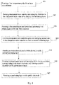
Fig. 4 is a flowchart of the method for manufacturing the thin-film transistors according to the present disclosure. - 1. Substrates; 2. Low-temperature polysilicon layers; 21. Doping region; 3. Insulating layers; 31. A first insulating layer; 32. A second insulating layer; 4. Gate; 5. Vias; 51.firstvias; 52. Second vias; 53. Third vias; 61. Source electrode; 62. Drain electrode; 7. planarization layer; 81. Public electrode; 82. Pixel electrode; 91. Buffer layer; 92. Passivation layer.
- The present invention will be further described in detail with reference to the accompanying drawings and specific embodiments in order to provide a better understanding of the technical solutions of the present invention by those skilled in the art.
- Some embodiments of the present disclosure provide a thin-film transistor, as shown in
Fig. 1 , comprising asubstrate 1, and a low-temperature polysilicon layer 2, a plurality ofinsulating layers 3 and agate 4 which are arranged on thesubstrate 1; wherein at least one insulating layer which is located on the side of the lowtemperature polysilicon layer 2 away from the substrate, are formed by organic material and hasvias 5. - The thin-film transistors according to the embodiments of the present disclosure include a plurality of
insulating layers 3, wherein at least one insulating layer arranged directly above the lowtemperature polysilicon layer 2 is formed by organic material, thus an exposing and developing process can be used to form vias in the organic material, which can effectively avoid the over-etching of the lowtemperature polysilicon layer 2 caused by dry etch process. - Some other embodiments of the present disclosure provide a thin-film transistor, as shown in
Figs. 2 and7 , comprising asubstrate 1, a low-temperature polysilicon layer 2 above thesubstrates 1, a firstinsulating layer 31 formed by the organic material and agate 4. Specifically, the firstinsulating layer 31 is located on the side of the low-temperature polysilicon layer 2 away from the substrates, and thegate 4 is located on the side of the firstinsulating layers 31 away from the substrates, wherein, the firstinsulating layers 31 havefirst vias 51. - The
Substrate 1 can be made of transparent materials such as glass and the like. As an active layer, the low-temperature polysilicon layer 2 is doped with phosphorus or boron at some positions to formdoping regions 21, so as to enhance its electronic properties. Thegate 4 is made of at least one selected from molybdenum, molybdenum niobium, aluminum, aluminum neodymium alloy, titanium or copper. The first insulatinglayer 31 located on the side of the lowtemperature polysilicon layer 2 away from the substrates, also referred as an interlayer insulating layer, is formed by organic material. In this way, thefirst vias 51 can be formed in the organic material by an exposing and developing process, which can effectively avoid the over-etching problem of the low-temperature polysilicon layer 2 caused by dry etch process. - The organic material may be selected from transparent polymer material, such as polymethyl methacrylate (PMMA), polyethylene terephthalate (PET), polycarbonate (PC), polyurethane (PU) and polyimide (PI). Since the above organic material is transparent, so the light transmittance of the final product would not be influenced.
- Particularly, since the above organic material is used as the insulating layers, the vias in the organic insulating layers could be formed by the exposure and developing process with mask plates, which not only avoids the over-etching problem of the polysilicon layer caused by the dry etch process, but also saves cost.
- Specifically, the organic insulating layer has a thickness from 1.5 µm to 3.0µmin the direction perpendicular to the
substrate 1. In other words, as shown inFig. 2 , the first insulatinglayers 31 has a thickness H1 in the range from 1.5µm to 3.0µm. - The organic insulation layer having a thickness H1 larger than 1.5µm could ensure the insulating properties between the
gate 4 above the organic insulation layer and the lowtemperature polysilicon layer 2 below the organic insulation layer. The organic insulating layer having a thickness H1 not more than 3.0µm could avoid increasing the thickness of the final products and thereby being more suitable for ultra-thin displays. - In an embodiment of the present disclosure, as shown in
fig. 2 , abuffer layer 91 is arranged between thesubstrate 1 and the lowtemperature polysilicon layer 2. Thebuffer layer 91 may be a single layer or a laminated layer with multiple sub-layers, and thebuffer layer 91 may be formed by silicon oxide or silicon nitride. - In another embodiment of the present disclosure, the insulating layers also comprise a second insulating
layer 32 which is arranged on the side of thegate 4 away from the substrate and hassecond vias 52. - In yet another embodiment of the present disclosure, the thin-film transistor also includes a
source electrode 61 and adrain electrode 62 arranged above the second insulatinglayer 32, and the source electrode and the drain electrode are in contact with the lowtemperature polysilicon layer 2 through thefirst vias 51 and thesecond vias 52. - As shown in
fig. 7 ,the second insulatinglayer 32 is arranged on thegate 4, also known as an insulating layer of thegate 4. The second insulatinglayer 32 may also be formed with organic material, and thesecond vias 52 are formed in the second insulatinglayer 32 by an exposing and developing process, which could effectively avoid the over-etching of the lowtemperature polysilicon layer 2. - In addition, since the
second vias 52 in the second insulatinglayer 32 are arranged at the positions corresponding to that of thefirst vias 51 in the first insulatinglayer 31, another advantage of the second insulatinglayer 32 formed by organic material is that thefirst vias 51 and thesecond vias 52 can be formed by one-step exposure technology, which can simplifies process and saves costs. - It is understood that the second insulating
layer 32 may also be made of silicon nitride or silicon oxide instead of organic material. That is to say, only the first insulatinglayer 31 closed to the lowtemperature polysilicon layer 2 is formed by organic material, so as to avoid the over-etching of the lowtemperature polysilicon layer 2. - Optionally, the orthographic projections of the first vias on the substrate at least partially coincide with those of the second vias on the substrate.
- In other words, in the direction perpendicular to the substrate, the
second vias 52 in the insulatinglayer 32 is aligned to thefirst vias 51 in the insulatinglayer 31, so one-step exposure technology can be used to form thesecond vias 52 and thefirst vias 51 when the first insulating layer and the second insulating layer both are formed by organic material, which can simplify process and save costs. - In an embodiment of the present disclosure, the thin-film transistor includes a
planarization layer 7 and apublic electrode 81, wherein theplanarization layer 7 is located on the side of thesource electrode 61 anddrain electrode 62 away from the substrates;third vias 53 are arranged in theplanarization layer 7 at the positons corresponding to the drain electrode, and thepublic electrode 81 is arranged above theplanarization layer 7 and contacts with thedrain electrode 62 through thethird vias 53. -
Fig. 7 shows theplanarization layer 7 on the side of the source electrode61 and drainelectrode 62 away from the substrate. Thethird vias 53 in theplanarization layer 7 and thepublic electrode 81 are located at the positions corresponding to the position of thedrain electrode 62. In addition, thepassivating layer 92 and thepixel electrode 82 are also shown inFig. 7 , and thepixel electrode 82 is connected to thedrain electrode 62 through the third vias and the vias in thepassivating layer 92. The size and thickness of the structures only are schematically shown in the drawings. In fact, the projected area of each layer on thesubstrate 1 may be the same or different, and the desired projected area of each layer can be achieved by an etching process. Similarly, the structure shown in the drawings do not limit the geometric shapes of each layer, such as the rectangle and trapezoid shown in the drawings or other shapes. - Some embodiments of the present disclosure also provide a method for manufacturing a thin-film transistor, comprising the following steps:
S01, as shown inFig.3 , amorphous silicon a-Si is deposited on a substrate made of transparent material such as glass, and then the amorphous silicon is crystallized to form polysilicon p-Si by "low temperature" crystallization process which makes a-Si in a depth of at least 50 Angstrom from the surface converting to p-Si. - Two common crystallization methods are excimer laser crystallization and metal induced crystallization. However, the method of the present disclosure for converting amorphous silicon into polysilicon is not limited to the above two methods, as long as the polysilicon transformation of the active layer can be achieved.
- Optionally, before the deposition of amorphous silicon, silicon oxide or silicon nitride is used to form the
buffer layer 91 on thesubstrate 1, as shown inFig. 2 . Thesubstrate 1 is pre-cleaned prior to forming thebuffer layer 91. Thebuffer layer 91 maybe a single layer or a laminated layer with multiple sub-layers. Then, the lowtemperature polysilicon layer 2 is formed on thebuffer layer 91. - S02, as shown in
Fig. 4 , the first insulatinglayer 31 is formed by organic material on thepolysilicon material layer 2, andfirst vias 51 are formed in the first insulatinglayer 31. - Specifically, S02 includes the following steps:
- S02a. The first organic film is formed by coating organic material on the polysilicon material layer. The organic material may be a transparent resin, such as anyone or any combination of polymethyl methacrylate (PMMA), polyethylene terephthalate (PET), polycarbonate (PC), polyurethane (PU), and polyimide (PI). It should be noted that the coated organic material maybe multilayer or monolayer or the coated organic material may be prepolymer of the above-mentioned polymers or a mixture solution of monomers of these polymers. Herein, PMMA prepolymer is used as an example in the detailed description for the subsequent steps, and other transparent resins are similar with PMMA.
- S02b, the first organic film (PMMA film) is cured at vacuum degree of 20 to 100 Pa, heating temperature of 80 to 130 °C for 90 s to 140 s;
- S02c, the first organic film obtained in S02b is exposed and developed with a mask at exposure energy of 150 to 300 MJ to form the first vias51.
- S02d,the first organic film obtained in S02c is further cured at atmospheric pressure and heating temperature of 200 °C to 250 °C for 40 min to 120 min to get the first insulating
layer 31. The first insulating layer has a thickness of 1.5µm to 3.0µm. - S03, as shown in
Fig. 5 , a first metal layer is formed and patterned to obtain thegate 4 of the thin-film transistor. Material for the Gate includes but not limited to one or more of Al, Mo, Cu, Ag, Cr, Ti, AINi, MoTi and the like. The gate has a thickness of 1500 to 6000 angstrom. - S04, as shown in
Fig. 6 , a second insulatinglayer 32 made of the organic material withsecond vias 52 are formed on thegate 4. - The second insulating layer is formed similarly according to the specific steps of S02. It should be noted that the
second vias 52 in the second insulatinglayer 32 is formed at the positions corresponding to those of thefirst vias 51 in the first insulatinglayer 31. Thus, the exposing and developing process for S02 and S04 can be completed in one step, which simplifies the technological processes and saves costs. In this case, only specific steps S02a and S02b are performed in step S02 to obtain the cured first organic film. - As mentioned above, the second insulating
layer 32 can also be made of silicon nitride or silicon oxide. In this case, only specific steps S02a and S02b are performed in the S02 step to obtain the cured first organic film layers; step S03 is performed subsequently to form the gate on the cured first organic film; and then the silicon nitride or silicon oxide is deposited to form the second insulating layer. - The vias in the second insulating layer formed by silicon nitride or silicon oxide are formed by a mask and etching process, and then the vias in the first insulating
layer 31 are formed by an exposing and developing process. - In addition to the above steps, the following steps usually are included during the manufacturing of the thin-film transistor:
- S05, a
source electrode 61 and adrain electrode 62 are formed on the second insulatinglayer 32. Specifically, thesource electrode 61 anddrain electrode 62 can be made of at least one of molybdenum, molybdenum niobium alloy, aluminum, aluminum neodymium alloy, titanium or copper. More specifically, the source and drain electrodes can be formed as metal films by puttering, thermal evaporation, plasma enhanced chemical vapor deposition (PECVD), low pressure chemical vapor deposition (LPCVD) and atmospheric pressure chemical vapor deposition (APCVD)or electron cyclotron resonance chemical vapor deposition (ECR-CVD). Then, a pattern including thesource electrode 61 anddrain electrode 62 is formed simultaneously by patterning process (film formation, exposure, development, wet etch or dry etch) with half tone mask (HTM) or gray tone mask (GTM). - S06, a
planarization layer 7 and apublic electrode 81 are formed on thesource electrode 61 anddrain electrode 62, and thethird vias 53 are formed in theplanarization layer 7 and thepublic electrode 81 at the positions corresponding to the position of thedrain electrode 62. Theplanarization layer 7 is mainly used to make the upper surface of the product planar, so as to deposit the electrode on the planar surface. - S07, a
passivating layer 92 is formed on thepubic electrode 81, and vias are formed in thepassivating layer 92. Thepassivating layer 92 may be a single layer or a laminated layer with multiple sub-layers, which may be formed by silicon oxide, silicon nitride, hafnium oxide or aluminum oxide. - S08, a
pixel electrode 82 is formed on thepassivating layer 92, and thepixel electrode 82 is connected with thedrain electrode 62 through the vias in the passivating layers 92 and thethird vias 53. - The insulating layers in the method according to this embodiment are made of organic material, the vias in the insulating layers do not need to be formed by a dry etch process, but just adopt an exposing and developing process. Therefore, it can effectively avoid the over-etching problem of the low temperature polysilicon layer below the insulating layers, and it can also increase the contact area and uniformity of the drain electrode and the low temperature polysilicon layer, thereby improving the electrical conductivity. In addition, the exposing and developing process of the second vias in the second insulating layer and the first vias in the first insulating layer can be completed in one step, which can greatly reduce the production cycle and improve the productivity of the equipment.
- Some embodiments of the present disclosure provide an array substrate comprising a plurality of the mentioned thin-film transistors arranged in an array.
- Some embodiments of the present disclosure provide a display apparatus comprising the mentioned array substrate. The display apparatus maybe liquid crystal display panel, electronic paper, mobile phone, tablet computer, television, display, laptop, digital photo frame, navigation device and any other products or components with display functions.
- Obviously, there can be many variations and improvements in the specific implementation conditions of the above embodiments, for example the specific parameters of each process step can be adjusted according to the require, and the specific steps of different products can be changed according to the actual situation.
- It is understood that the above embodiments are only exemplary ones used to illustrate the principles of the present disclosure, but the present disclosure is not limited to these. For ordinary technical personnel in this field, various variations and improvements can be made without breaking away from the spirit and essence of the present disclosure, and these variations and improvements are also regarded as the scope of protection of the present disclosure.
Claims (13)
- A thin-film transistor including a substrate, and a low temperature polysilicon layer, a plurality of insulating layers and a gate disposed on the substrate;
Wherein at least one of the plurality of insulating layers which contact with the side of the low temperature polysilicon layers away from the substrate, comprises organic material and has vias. - The thin-film transistor according to claim 1, wherein the insulating layers include a first insulating layer with first vias; the first insulating layer is arranged between the low temperature polysilicon layer and the gate; and the gate is located on the side of the first insulating layer away from the substrate.
- The thin-film transistors according to claim 2, wherein the insulating layers also include a second insulating layer with second vias and the second insulating layer is located on the side of the gate away from the substrate.
- The thin-film transistors according to claim 3, further comprising a source electrode and a drain electrode, wherein the source electrode and the drain electrode are located on the side of the second insulating layer away from the substrate and the source electrode and the drain electrode are in contact with the low temperature polysilicon layer through the first and second vias.
- The thin-film transistors according to claim 4, wherein the orthographic projections of the first vias on the substrate at least partially coincide with the orthographic projections of the second vias on the substrate.
- The thin-film transistors according to claim 4, further comprising: a planarization layer, a public electrode and a pixel electrode,
wherein the planarization layer is located on the side of the source and drain electrodes away from the substrate;
the planarization layer and the public electrode have third vias at a position corresponding to the drain electrode; and
the pixel electrode are in connect with the drain electrode through the third vias. - The thin-film transistors according to claim 1, wherein the organic material is anyone or any combination of polymethyl methacrylate, polyethylene terephthalate, polycarbonate, polyurethane and polyimide.
- The thin-film transistors according to claim 1, wherein the insulting layer has a thickness of 1.5µm to 3.0µm in the direction perpendicular to the substrate.
- An array substrate including a plurality of thin-film transistors arranged in an array, and the plurality of thin-film transistors include the thin-film transistor according to anyone of claims 1-8.
- A display device including the array substrate according to claim 9.
- A method for manufacturing a thin-film transistor comprising the following steps:forming a low temperature polysilicon layer on a substrate;forming an organic insulating layer on the side of the low temperature polysilicon layer away from the substrate, and forming vias in the organic insulating layer;forming a first metal layer and patterning it to obtain agate of the thin-film transistor.
- The method for manufacturing a thin-film transistor according to claim 11, where informing an organic insulating layer with vias comprises the following steps:coating organic material on the low temperature polysilicon layer to form a film;performing a first curing of the obtained film;exposing and developing the film after the first curing to form the vias;.performing a second curing of the film with the vias to form the organic insulating layer.
- The method for manufacturing a thin-film transistor according to claim 12, wherein the first curing is carried out at vacuum degree of 20 Pa to 100 Pa and heating temperature of 80 °C to 130 °C for 90 s to 140 s and the second curing is carried out at atmospheric pressure and heating temperature of 200 °C to 250 °C for 40 min to 120 min.
Applications Claiming Priority (2)
| Application Number | Priority Date | Filing Date | Title |
|---|---|---|---|
| CN201711137106.6A CN109801923A (en) | 2017-11-16 | 2017-11-16 | A kind of thin film transistor (TFT) and preparation method thereof, array substrate, display device |
| PCT/CN2018/107269 WO2019095857A1 (en) | 2017-11-16 | 2018-09-25 | Thin-film transistor and preparation method therefor, array substrate, and display device |
Publications (2)
| Publication Number | Publication Date |
|---|---|
| EP3712943A1 true EP3712943A1 (en) | 2020-09-23 |
| EP3712943A4 EP3712943A4 (en) | 2021-08-11 |
Family
ID=66539971
Family Applications (1)
| Application Number | Title | Priority Date | Filing Date |
|---|---|---|---|
| EP18855143.6A Withdrawn EP3712943A4 (en) | 2017-11-16 | 2018-09-25 | THIN-FILM TRANSISTOR AND MANUFACTURING METHOD FOR IT, ARRAY SUBSTRATE AND DISPLAY DEVICE |
Country Status (4)
| Country | Link |
|---|---|
| US (1) | US11588055B2 (en) |
| EP (1) | EP3712943A4 (en) |
| CN (1) | CN109801923A (en) |
| WO (1) | WO2019095857A1 (en) |
Family Cites Families (14)
| Publication number | Priority date | Publication date | Assignee | Title |
|---|---|---|---|---|
| DE19712233C2 (en) | 1996-03-26 | 2003-12-11 | Lg Philips Lcd Co | Liquid crystal display and manufacturing method therefor |
| US8941569B2 (en) * | 2010-02-24 | 2015-01-27 | Sharp Kabushiki Kaisha | Liquid crystal display device, television receiver and display method employed in liquid crystal display device |
| KR101097344B1 (en) | 2010-03-09 | 2011-12-23 | 삼성모바일디스플레이주식회사 | Method of manufacturing flexible display apparatus |
| KR101963229B1 (en) * | 2011-12-05 | 2019-03-29 | 삼성전자주식회사 | Folderble thin film transistor |
| KR102175285B1 (en) * | 2013-08-14 | 2020-11-09 | 삼성디스플레이 주식회사 | Display panel and method of manufacturing the same |
| CN103456745B (en) * | 2013-09-10 | 2016-09-07 | 北京京东方光电科技有限公司 | A kind of array base palte and preparation method thereof, display device |
| CN103779360B (en) * | 2014-02-12 | 2017-02-15 | 鄂尔多斯市源盛光电有限责任公司 | Display substrate and manufacturing method and display device of display substrate |
| CN103985637B (en) | 2014-04-30 | 2017-02-01 | 京东方科技集团股份有限公司 | Low-temperature polycrystalline silicon thin film transistor, manufacturing method thereof and display device |
| CN104103646A (en) * | 2014-06-30 | 2014-10-15 | 京东方科技集团股份有限公司 | Low temperature poly-silicon thin film transistor array substrate and fabrication method thereof and display device |
| KR102285384B1 (en) * | 2014-09-15 | 2021-08-04 | 삼성디스플레이 주식회사 | Thin film transistor array substrate and manufacturing method for the same and display |
| KR102245394B1 (en) * | 2015-03-27 | 2021-04-28 | 도레이 카부시키가이샤 | Photosensitive resin composition for a thin film transistor, a cured film, a thin film transistor, a liquid crystal display device or an organic electroluminescent display device, a method of manufacturing a cured film, a method of manufacturing a thin film transistor, and a method of manufacturing a liquid crystal display device or an organic electroluminescent display device |
| US9502435B2 (en) * | 2015-04-27 | 2016-11-22 | International Business Machines Corporation | Hybrid high electron mobility transistor and active matrix structure |
| TWI616792B (en) * | 2017-05-03 | 2018-03-01 | 友達光電股份有限公司 | Touch display device manufacturing method |
| CN207367976U (en) * | 2017-11-16 | 2018-05-15 | 京东方科技集团股份有限公司 | A kind of thin film transistor (TFT), array base palte, display device |
-
2017
- 2017-11-16 CN CN201711137106.6A patent/CN109801923A/en active Pending
-
2018
- 2018-09-25 EP EP18855143.6A patent/EP3712943A4/en not_active Withdrawn
- 2018-09-25 US US16/335,065 patent/US11588055B2/en active Active
- 2018-09-25 WO PCT/CN2018/107269 patent/WO2019095857A1/en not_active Ceased
Also Published As
| Publication number | Publication date |
|---|---|
| CN109801923A (en) | 2019-05-24 |
| US20210328073A1 (en) | 2021-10-21 |
| EP3712943A4 (en) | 2021-08-11 |
| US11588055B2 (en) | 2023-02-21 |
| WO2019095857A1 (en) | 2019-05-23 |
Similar Documents
| Publication | Publication Date | Title |
|---|---|---|
| CN106057827B (en) | array substrate, preparation method thereof and display device | |
| KR101533098B1 (en) | Thin film transistor and method of manufacturing thereof | |
| US10128281B2 (en) | Array substrate, fabrication method thereof and display device | |
| US8962404B2 (en) | Method for manufacturing fan-out lines on array substrate | |
| US10381382B2 (en) | Array substrate, method for manufacturing the same and display device | |
| US7755708B2 (en) | Pixel structure for flat panel display | |
| CN105070684B (en) | Preparation method of array substrate, array substrate and display device | |
| US20150221669A1 (en) | Thin FilmTransistor, Array Substrate, And Manufacturing Method Thereof | |
| JP2019537282A (en) | Array substrate, method of manufacturing the same, and display device | |
| EP2709159B1 (en) | Fabricating method of thin film transistor, fabricating method of array substrate and display device | |
| US20170110587A1 (en) | Array substrate and manufacturing method thereof, display panel, display device | |
| TW201225279A (en) | Organic light-emitting display device and method of manufacturing the same | |
| US8551822B2 (en) | Method for manufacturing array substrate | |
| EP3627543A1 (en) | Method for manufacturing tft substrate | |
| CN104133313A (en) | Array substrate, manufacturing method thereof and liquid crystal display device | |
| US20210066504A1 (en) | Thin film transistor and manufacturing method thereof and display device | |
| WO2015010404A1 (en) | Thin film transistor, manufacturing method thereof, array substrate and display device | |
| CN107134497B (en) | Thin film transistor, method for manufacturing the same, and display substrate | |
| US10622387B2 (en) | Method for manufacturing active array switch | |
| CN100483233C (en) | Pixel structure of flat panel display and manufacturing method thereof | |
| US11588055B2 (en) | Thin-film transistor and method for manufacturing the same, array substrates, display devices | |
| EP3163620B1 (en) | Low temperature poly-silicon thin film transistor array substrate and manufacturing method therefor and display device | |
| WO2014117444A1 (en) | Array substrate and manufacturing method thereof, display device | |
| CN102931139A (en) | Array substrate and manufacture method and display device thereof | |
| CN207367976U (en) | A kind of thin film transistor (TFT), array base palte, display device |
Legal Events
| Date | Code | Title | Description |
|---|---|---|---|
| STAA | Information on the status of an ep patent application or granted ep patent |
Free format text: STATUS: UNKNOWN |
|
| STAA | Information on the status of an ep patent application or granted ep patent |
Free format text: STATUS: THE INTERNATIONAL PUBLICATION HAS BEEN MADE |
|
| PUAI | Public reference made under article 153(3) epc to a published international application that has entered the european phase |
Free format text: ORIGINAL CODE: 0009012 |
|
| STAA | Information on the status of an ep patent application or granted ep patent |
Free format text: STATUS: REQUEST FOR EXAMINATION WAS MADE |
|
| 17P | Request for examination filed |
Effective date: 20190320 |
|
| AK | Designated contracting states |
Kind code of ref document: A1 Designated state(s): AL AT BE BG CH CY CZ DE DK EE ES FI FR GB GR HR HU IE IS IT LI LT LU LV MC MK MT NL NO PL PT RO RS SE SI SK SM TR |
|
| AX | Request for extension of the european patent |
Extension state: BA ME |
|
| DAV | Request for validation of the european patent (deleted) | ||
| DAX | Request for extension of the european patent (deleted) | ||
| A4 | Supplementary search report drawn up and despatched |
Effective date: 20210709 |
|
| RIC1 | Information provided on ipc code assigned before grant |
Ipc: H01L 27/12 20060101AFI20210705BHEP Ipc: H01L 29/786 20060101ALI20210705BHEP Ipc: H01L 21/336 20060101ALI20210705BHEP Ipc: H01L 29/49 20060101ALI20210705BHEP |
|
| STAA | Information on the status of an ep patent application or granted ep patent |
Free format text: STATUS: EXAMINATION IS IN PROGRESS |
|
| STAA | Information on the status of an ep patent application or granted ep patent |
Free format text: STATUS: THE APPLICATION HAS BEEN WITHDRAWN |
|
| 17Q | First examination report despatched |
Effective date: 20240521 |
|
| 18W | Application withdrawn |
Effective date: 20240606 |