EP3712936A1 - Flexible base design for chipset heat sink - Google Patents
Flexible base design for chipset heat sink Download PDFInfo
- Publication number
- EP3712936A1 EP3712936A1 EP19188769.4A EP19188769A EP3712936A1 EP 3712936 A1 EP3712936 A1 EP 3712936A1 EP 19188769 A EP19188769 A EP 19188769A EP 3712936 A1 EP3712936 A1 EP 3712936A1
- Authority
- EP
- European Patent Office
- Prior art keywords
- heat sink
- heat
- chipset
- central cylinder
- contact
- Prior art date
- Legal status (The legal status is an assumption and is not a legal conclusion. Google has not performed a legal analysis and makes no representation as to the accuracy of the status listed.)
- Granted
Links
Images

Classifications
-
- H—ELECTRICITY
- H10—SEMICONDUCTOR DEVICES; ELECTRIC SOLID-STATE DEVICES NOT OTHERWISE PROVIDED FOR
- H10W—GENERIC PACKAGES, INTERCONNECTIONS, CONNECTORS OR OTHER CONSTRUCTIONAL DETAILS OF DEVICES COVERED BY CLASS H10
- H10W40/00—Arrangements for thermal protection or thermal control
- H10W40/60—Securing means for detachable heating or cooling arrangements, e.g. clamps
- H10W40/611—Bolts or screws
-
- H—ELECTRICITY
- H10—SEMICONDUCTOR DEVICES; ELECTRIC SOLID-STATE DEVICES NOT OTHERWISE PROVIDED FOR
- H10W—GENERIC PACKAGES, INTERCONNECTIONS, CONNECTORS OR OTHER CONSTRUCTIONAL DETAILS OF DEVICES COVERED BY CLASS H10
- H10W40/00—Arrangements for thermal protection or thermal control
- H10W40/70—Fillings or auxiliary members in containers or in encapsulations for thermal protection or control
- H10W40/77—Auxiliary members characterised by their shape
- H10W40/774—Pistons, e.g. spring-loaded members
-
- H—ELECTRICITY
- H10—SEMICONDUCTOR DEVICES; ELECTRIC SOLID-STATE DEVICES NOT OTHERWISE PROVIDED FOR
- H10W—GENERIC PACKAGES, INTERCONNECTIONS, CONNECTORS OR OTHER CONSTRUCTIONAL DETAILS OF DEVICES COVERED BY CLASS H10
- H10W40/00—Arrangements for thermal protection or thermal control
- H10W40/20—Arrangements for cooling
- H10W40/22—Arrangements for cooling characterised by their shape, e.g. having conical or cylindrical projections
-
- F—MECHANICAL ENGINEERING; LIGHTING; HEATING; WEAPONS; BLASTING
- F28—HEAT EXCHANGE IN GENERAL
- F28D—HEAT-EXCHANGE APPARATUS, NOT PROVIDED FOR IN ANOTHER SUBCLASS, IN WHICH THE HEAT-EXCHANGE MEDIA DO NOT COME INTO DIRECT CONTACT
- F28D15/00—Heat-exchange apparatus with the intermediate heat-transfer medium in closed tubes passing into or through the conduit walls ; Heat-exchange apparatus employing intermediate heat-transfer medium or bodies
- F28D15/02—Heat-exchange apparatus with the intermediate heat-transfer medium in closed tubes passing into or through the conduit walls ; Heat-exchange apparatus employing intermediate heat-transfer medium or bodies in which the medium condenses and evaporates, e.g. heat pipes
-
- F—MECHANICAL ENGINEERING; LIGHTING; HEATING; WEAPONS; BLASTING
- F28—HEAT EXCHANGE IN GENERAL
- F28F—DETAILS OF HEAT-EXCHANGE AND HEAT-TRANSFER APPARATUS, OF GENERAL APPLICATION
- F28F3/00—Plate-like or laminated elements; Assemblies of plate-like or laminated elements
-
- H—ELECTRICITY
- H10—SEMICONDUCTOR DEVICES; ELECTRIC SOLID-STATE DEVICES NOT OTHERWISE PROVIDED FOR
- H10W—GENERIC PACKAGES, INTERCONNECTIONS, CONNECTORS OR OTHER CONSTRUCTIONAL DETAILS OF DEVICES COVERED BY CLASS H10
- H10W40/00—Arrangements for thermal protection or thermal control
- H10W40/20—Arrangements for cooling
- H10W40/25—Arrangements for cooling characterised by their materials
- H10W40/258—Metallic materials
-
- H—ELECTRICITY
- H10—SEMICONDUCTOR DEVICES; ELECTRIC SOLID-STATE DEVICES NOT OTHERWISE PROVIDED FOR
- H10W—GENERIC PACKAGES, INTERCONNECTIONS, CONNECTORS OR OTHER CONSTRUCTIONAL DETAILS OF DEVICES COVERED BY CLASS H10
- H10W40/00—Arrangements for thermal protection or thermal control
- H10W40/40—Arrangements for thermal protection or thermal control involving heat exchange by flowing fluids
- H10W40/43—Arrangements for thermal protection or thermal control involving heat exchange by flowing fluids by flowing gases, e.g. forced air cooling
-
- H—ELECTRICITY
- H10—SEMICONDUCTOR DEVICES; ELECTRIC SOLID-STATE DEVICES NOT OTHERWISE PROVIDED FOR
- H10W—GENERIC PACKAGES, INTERCONNECTIONS, CONNECTORS OR OTHER CONSTRUCTIONAL DETAILS OF DEVICES COVERED BY CLASS H10
- H10W40/00—Arrangements for thermal protection or thermal control
- H10W40/70—Fillings or auxiliary members in containers or in encapsulations for thermal protection or control
- H10W40/73—Fillings or auxiliary members in containers or in encapsulations for thermal protection or control for cooling by change of state
-
- H—ELECTRICITY
- H10—SEMICONDUCTOR DEVICES; ELECTRIC SOLID-STATE DEVICES NOT OTHERWISE PROVIDED FOR
- H10W—GENERIC PACKAGES, INTERCONNECTIONS, CONNECTORS OR OTHER CONSTRUCTIONAL DETAILS OF DEVICES COVERED BY CLASS H10
- H10W40/00—Arrangements for thermal protection or thermal control
- H10W40/70—Fillings or auxiliary members in containers or in encapsulations for thermal protection or control
- H10W40/77—Auxiliary members characterised by their shape
-
- H—ELECTRICITY
- H10—SEMICONDUCTOR DEVICES; ELECTRIC SOLID-STATE DEVICES NOT OTHERWISE PROVIDED FOR
- H10W—GENERIC PACKAGES, INTERCONNECTIONS, CONNECTORS OR OTHER CONSTRUCTIONAL DETAILS OF DEVICES COVERED BY CLASS H10
- H10W40/00—Arrangements for thermal protection or thermal control
- H10W40/70—Fillings or auxiliary members in containers or in encapsulations for thermal protection or control
- H10W40/77—Auxiliary members characterised by their shape
- H10W40/772—Bellows
-
- H—ELECTRICITY
- H10—SEMICONDUCTOR DEVICES; ELECTRIC SOLID-STATE DEVICES NOT OTHERWISE PROVIDED FOR
- H10W—GENERIC PACKAGES, INTERCONNECTIONS, CONNECTORS OR OTHER CONSTRUCTIONAL DETAILS OF DEVICES COVERED BY CLASS H10
- H10W40/00—Arrangements for thermal protection or thermal control
- H10W40/20—Arrangements for cooling
- H10W40/231—Arrangements for cooling characterised by their places of attachment or cooling paths
-
- H—ELECTRICITY
- H10—SEMICONDUCTOR DEVICES; ELECTRIC SOLID-STATE DEVICES NOT OTHERWISE PROVIDED FOR
- H10W—GENERIC PACKAGES, INTERCONNECTIONS, CONNECTORS OR OTHER CONSTRUCTIONAL DETAILS OF DEVICES COVERED BY CLASS H10
- H10W40/00—Arrangements for thermal protection or thermal control
- H10W40/60—Securing means for detachable heating or cooling arrangements, e.g. clamps
-
- H—ELECTRICITY
- H10—SEMICONDUCTOR DEVICES; ELECTRIC SOLID-STATE DEVICES NOT OTHERWISE PROVIDED FOR
- H10W—GENERIC PACKAGES, INTERCONNECTIONS, CONNECTORS OR OTHER CONSTRUCTIONAL DETAILS OF DEVICES COVERED BY CLASS H10
- H10W40/00—Arrangements for thermal protection or thermal control
- H10W40/60—Securing means for detachable heating or cooling arrangements, e.g. clamps
- H10W40/625—Clamping parts not primarily conducting heat
Definitions
- This disclosure pertains to heat sinks that provide improved thermal contact with a chipset.
- Heat sinks are a common thermal solution for removing heat from chipsets. In operation, heat transfer between the chipset and the heat sink is best performed by conduction. It is therefore important to keep good contact between the base of the heat sink and the chipset. Factors that influence contact status include: (1) sufficient surface flatness of the heat sink base and chipset surface; (2) using thermal interface material in the contact area between the heat sink and the chipset; and (3) appropriate loading force to maintain contact between the heat sink and the chipset.
- chipsets may have a defect in that their surface configuration can deviate from the desired surface flatness required for intimate contact with the base of the heat sink. Even if originally manufactured with an acceptable flatness, the chipset may develop an upper surface with a concave profile. The chipset will not be flat during use because of the accumulative stress of manufacturing temperature cycles and also from stress caused by heat from the systems printed circuit board ("PCB").
- a typical base for a heat sink is one formed from a good heat conducting metal, such as copper. While the copper heat sink base will maintain its flatness, the periphery (or at least some edges of the chipset) may grow to form a concave profile while the copper base of the heat sink remains flat.
- conductive heat sink bases are formed of a metal in a manner that will flex to allow the heat sink base to contour itself to the surface of the chipset with which it is associated.
- the metal can be selected from a highly heat conductive metal, such as copper.
- a heat sink base is made flexible by providing a series of concentric rings in the form of valleys or depressions on the side of the heat sink base, opposite the contact side of the heat sink base with the chipset.
- a heat sink base is made flexible by providing a series of concentric rings in the form of valleys or depressions on the side of the heat sink base, opposite the contact side of the heat sink base with the chipset.
- the heat sink base is made flexible by further providing a cylinder of heat conductive metal at the center of the concentric rings.
- At least the central cylinder will remain in contact with at least one fin when the heat sink base is flexed to transfer heat by conduction between the heat sink and the fin.
- the flexible heat sink base is provided with a biasing device, such as a spring, exerting force on the cylinder to cause the heat sink base to deform.
- a biasing device such as a spring
- the spring may be H-shaped, including a central portion having four arms extending from the central portion. Screws may be employed to align the spring, the fin and the heat sink base, and exert a force towards a chipset.
- a heat sink base that is made flexible by providing a series of concentric rings in the form of valleys or depressions on the side of the heat sink base, opposite the contact side of the heat sink base with the chipset.
- the heat sink base is made flexible by further providing a plurality of depressions in addition to the series of concentric rings, into which depressions are placed at least one heat pipe.
- a combination of a flexible heat sink formed of a heat conductive metal in a first, flat configuration, is placed into position so as to face a source of heat, such as a concave surface of a chipset.
- the heat sink base is flexed without breaking, into a second, convex configuration, such that the heat sink base will more closely conform to the concave surface of the chipset in order to transfer heat by conduction between the chipset and the heat sink.
- a series of concentric grooves in a surface of the heat sink base opposite the surface contacting the chipset is provided with a metal cylinder at the center of the concentric grooves. The cylinder remains in contact with at least one fin in both the first and second configurations.
- a spring such as an H-shaped spring, may provide a biasing force on the cylinder to flex the heat sink into the second configuration.
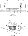
- FIG. 1 illustrates a typical heat sink assembly 10 in contact with a chipset 12.
- Chipset 12 is connected to a printed circuit board (PCB) 14.
- PCB printed circuit board
- Chipset 12 may be any collection or grouping of integrated circuits, such as a switch, audio or graphics chip, the so-called north bridge and south bridge chips on a motherboard and similar devices. The specific configuration or use of the chipset is not limited by these examples.
- An upper surface 13 of chipset 12 was designed to be flat to contact the flat surface 15 of heat sink base 11.
- the heat sink base 11 is in contact with at least one fin 17 to dissipate the heat transferred to heat sink base 11.
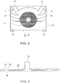
- FIG. 2 is a perspective view of a heat base 24, according to the present disclosure.
- Heat base 24 may be formed of a highly heat conductive metal having a heat conductivity in the range of 0.50-0.99 (cal/sec)/ (cm 2 C/cm), such as copper and aluminum, in a manner similar to the materials used as heat sinks in the past.
- the metal is provided with a series of concentric grooves 26 in the surface 25 opposite the surface intended to contact the chipset 12.
- a metal cylinder 27 is provided at the center of the series of concentric grooves 26.
- Metal cylinder 27 is formed of a highly heat conductive metal such as copper, and in one embodiment, is integral with heat base 24.
- a plurality of depressions 28, 29, 30, 31 may also be formed in surface 25 of heat base 24 to accommodate heat pipes 32, 33, 34, 35 (shown in FIG. 6 ).
- a plurality of apertures 40, 41, 42, 43 are provided in heat base 24 to accommodate fasteners, such as screws (as described below).
- FIG. 4 illustrates, in side view, the cross-sectional shape of the series of grooves 26.
- Grooves 26 do not extend to the lower surface 36 of heat sink base 24 such that lower surface 36 comprises an uninterrupted surface of highly heat conductive metal.
- Lower surface 36 of heat sink base 24 is designed to come into contact with chipset 12. While we have illustrated the concentric series of grooves 26 having a quadrilateral shape, such is by way of example only.
- the groove shape and depth may be of any shape and depth provided that the function and purpose of the series of concentric grooves 26 allows the lower surface 36 of heat sink base 24 to be continuous and uninterrupted and flex as described below.
- a metal spring 37 as shown in FIG. 5 is provided to create a biasing force to flex lower surface 36 of heat sink base 24 ( FIG 4 ).
- Metal spring 37 is illustrated in the form of an H-shape, having a central portion 38 and four arms 44, 45, 46, 47, extending from the central portion 38. Each of the arms 44, 45, 46 and 47 are held against fin 48 by screws. While we have illustrated spring 37 as H-shaped, it will be readily seen by those skilled in the art that other spring shapes, such as those that can create geometric center force to press central metal cylinder 27, such as X-shaped springs and even star-shaped and other multi-armed springs can be employed to create the geometric center force to press central cylinder 27.
- FIG. 6 illustrates, in a side, cross-sectional, view the assembled heat sink 50 of the disclosure.
- Screws 51, 52 hold metal spring 37 in place such that the central portion 38 of spring 37 overlies the circular cylinder 27.
- the spring 37 will provide a bias upon circular cylinder 27 to provide an outwardly bowing of lower surface 36 of heat sink base 24.
- the series of concentric grooves 26 will permit the upper surface 25 of heat sink base 24 to absorb the flex of lower surface 36, without stressing the highly heat conductive metal forming the heat sink base 24 to the point of breaking.
- at least one fin 48 is provided to remove heat from the heat sink by convection.
- central cylinder 27 It is important that the central cylinder 27 remain in contact with the at least one fin 48 in order to maintain conductive heat transfer between the heat base 24 and at least one fin 48. By maintaining the central cylinder 27 and the at least one fin 48 in contact with each other, conductive heat transfer will be maintained, even though lower surface 36 may reduce its contact with the at least one fin 48 as shown in FIG. 7 .
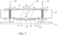
- FIG. 7 illustrates the heat sink 50 assembled against the chipset 12 having a concave upper surface.
- the screws 51, 52 when tightened provide a loading force in the direction of arrows 62, 63 against the arms 45, 46 of the H-shaped spring 37.
- the central portion 38 of spring 37 bears upon the central cylinder 27 imposing a downwardly directed force in the direction of arrow 53.
- This downwardly directed force on central cylinder 27 causes central cylinder 27 to flex the upper surface 25 as well as the lower surface 36 of heat sink base 24 to form a convex or smiley shape 55 conforming closely to the concave shape of upper surface 13 of chipset 12.
- the flexing of lower surface 36 of heat base 24 reduces or eliminates the air gap 19 and restores contact between heat sink base 24 and chipset 12 to promote conductive cooling.
- a thermal interface material 65 may be inserted between the concave upper surface 13 of chipset 12 and the flexed surface lower surface 36 of heat sink base 24.
- Central cylinder 27 will remain in contact with the at least one fin 48, even when surface 25 of heat base 24 is flexed into reduced contact with the at least one fin 48 to continue to transfer heat from heat base 24 to the at least one fin 48 through central cylinder 27.
- the at least one fin 48 will remove heat by convective cooling, usually with the aid of at least one fan (not shown) blowing, or drawing a cooling stream of air over the at least one fin 48.
- the design of the at least one fin 48 is outside the scope of this disclosure as known designs of cooling fins can be substituted for the at least one fin 48.
Landscapes
- Engineering & Computer Science (AREA)
- Physics & Mathematics (AREA)
- Thermal Sciences (AREA)
- Mechanical Engineering (AREA)
- General Engineering & Computer Science (AREA)
- Life Sciences & Earth Sciences (AREA)
- Sustainable Development (AREA)
- Cooling Or The Like Of Semiconductors Or Solid State Devices (AREA)
- Cooling Or The Like Of Electrical Apparatus (AREA)
Abstract
Description
- This disclosure pertains to heat sinks that provide improved thermal contact with a chipset.
- Heat sinks are a common thermal solution for removing heat from chipsets. In operation, heat transfer between the chipset and the heat sink is best performed by conduction. It is therefore important to keep good contact between the base of the heat sink and the chipset. Factors that influence contact status include: (1) sufficient surface flatness of the heat sink base and chipset surface; (2) using thermal interface material in the contact area between the heat sink and the chipset; and (3) appropriate loading force to maintain contact between the heat sink and the chipset.
- However, chipsets may have a defect in that their surface configuration can deviate from the desired surface flatness required for intimate contact with the base of the heat sink. Even if originally manufactured with an acceptable flatness, the chipset may develop an upper surface with a concave profile. The chipset will not be flat during use because of the accumulative stress of manufacturing temperature cycles and also from stress caused by heat from the systems printed circuit board ("PCB"). A typical base for a heat sink is one formed from a good heat conducting metal, such as copper. While the copper heat sink base will maintain its flatness, the periphery (or at least some edges of the chipset) may grow to form a concave profile while the copper base of the heat sink remains flat. This growth along the periphery of the chipset will cause an air gap to form between the concave surface of the chipset (intermediate its periphery) and the flat base of the heat sink. The contact between chipset and heat sink is reduced, as well as the conduction between these elements. Thus, reduced contact between chipset and base of the heat sink reduces conductive heat transfer between the base of the heat sink and the chipset.
- Thus, there is a need for an improved heat sink base that will accommodate changes in the flatness of the chip set.
- According to one embodiment of this disclosure, conductive heat sink bases are formed of a metal in a manner that will flex to allow the heat sink base to contour itself to the surface of the chipset with which it is associated. The metal can be selected from a highly heat conductive metal, such as copper.
- According to another embodiment of this disclosure, a heat sink base is made flexible by providing a series of concentric rings in the form of valleys or depressions on the side of the heat sink base, opposite the contact side of the heat sink base with the chipset.
- According to a still further embodiment of this disclosure, a heat sink base is made flexible by providing a series of concentric rings in the form of valleys or depressions on the side of the heat sink base, opposite the contact side of the heat sink base with the chipset. The heat sink base is made flexible by further providing a cylinder of heat conductive metal at the center of the concentric rings.
- According to a still further embodiment of this disclosure, at least the central cylinder will remain in contact with at least one fin when the heat sink base is flexed to transfer heat by conduction between the heat sink and the fin.
- According to a still further embodiment of this disclosure, the flexible heat sink base is provided with a biasing device, such as a spring, exerting force on the cylinder to cause the heat sink base to deform. The spring may be H-shaped, including a central portion having four arms extending from the central portion. Screws may be employed to align the spring, the fin and the heat sink base, and exert a force towards a chipset.
- According to a still further embodiment of this disclosure, a heat sink base that is made flexible by providing a series of concentric rings in the form of valleys or depressions on the side of the heat sink base, opposite the contact side of the heat sink base with the chipset. The heat sink base is made flexible by further providing a plurality of depressions in addition to the series of concentric rings, into which depressions are placed at least one heat pipe.
- In a further embodiment, a combination of a flexible heat sink, formed of a heat conductive metal in a first, flat configuration, is placed into position so as to face a source of heat, such as a concave surface of a chipset. The heat sink base is flexed without breaking, into a second, convex configuration, such that the heat sink base will more closely conform to the concave surface of the chipset in order to transfer heat by conduction between the chipset and the heat sink. A series of concentric grooves in a surface of the heat sink base opposite the surface contacting the chipset is provided with a metal cylinder at the center of the concentric grooves. The cylinder remains in contact with at least one fin in both the first and second configurations. A spring, such as an H-shaped spring, may provide a biasing force on the cylinder to flex the heat sink into the second configuration.
- A method of utilizing the above-described heat sink to conductively transfer heat from the chipset to the heat sink is also described.
- The above summary is not intended to represent each embodiment or every aspect of the present disclosure. Rather, the foregoing summary merely provides an example of some of the novel aspects and features set forth herein. The above features and advantages, and other features and advantages of the present disclosure, will be readily apparent from the following detailed description of representative embodiments and modes for carrying out the present invention, when taken in connection with the accompanying drawings and the appended claims.
- The disclosure, and its advantages and drawings, will be better understood from the following description of exemplary embodiments together with reference to the accompanying drawings. These drawings depict only exemplary embodiments, and are therefore not to be considered as limitations on the scope of the various embodiments or claims.
-
FIG. 1 (Prior Art) is a schematic illustration of a chipset that has a developed a concave profile in its upper surface and is causing an air gap to form between the chipset and the base of a heat sink. -
FIG. 2 is a schematic, perspective view of a heat sink base formed according to the present disclosure. -
FIG. 3 is a top view ofFIG. 2 . -
FIG. 4 is a side view, in cross-section, ofFIG. 3 . -
FIG. 5 is a perspective view of a metal spring to provide a biasing force on the heat sink base ofFIG. 4 . -
FIG. 6 is a side view in cross-section of the heat sink of the present disclosure. -
FIG. 7 is a side view of the heat sink ofFIG. 6 in contact with a chipset having a concave upper surface. - The present inventions can be embodied in many different forms. Representative embodiments are shown in the drawings, and will herein be described in detail. These embodiments are examples or illustrations of the principles of the disclosure but are not intended to limit its broad aspects. To that extent, elements and limitations that are disclosed, for example, in the Abstract, Summary, and Detailed Description sections, but not explicitly set forth in the claims, should not be incorporated into the claims, singly or collectively, by implication, inference, or otherwise. For purposes of the present detailed description, unless specifically disclaimed, the singular includes the plural and vice versa; and the word "including" means "including without limitation." Moreover, words of approximation, such as "about," "almost," "substantially," "approximately," and the like, can be used herein to mean "at," "near," or "nearly at," or "within 3-5% of," or "within acceptable manufacturing tolerances," or any logical combination thereof, for example. For the convenience of the reader, like elements in the various views of the drawings will be similarly numbered.
-
FIG. 1 (Prior Art) illustrates a typicalheat sink assembly 10 in contact with achipset 12.Chipset 12 is connected to a printed circuit board (PCB) 14.Chipset 12 may be any collection or grouping of integrated circuits, such as a switch, audio or graphics chip, the so-called north bridge and south bridge chips on a motherboard and similar devices. The specific configuration or use of the chipset is not limited by these examples. Anupper surface 13 ofchipset 12 was designed to be flat to contact theflat surface 15 ofheat sink base 11. Theheat sink base 11 is in contact with at least onefin 17 to dissipate the heat transferred to heatsink base 11. However, the stresses caused by manufacturing and use of thechipset 12 frequently cause theupper surface 13 ofchipset 12 to deform, here illustrated assides upper surface 13 inchipset 12. This concave upper surface forms anair gap 19 betweenlower surface 15 ofheat sink base 11 and theupper surface 13 ofchipset 12. Thisair gap 19 reduces the conductive heat transfer betweenchipset 12 andheat sink base 11, thereby reducing the overall thermal cooling ofheat sink assembly 10.Screws arrows heat sink base 11 andchipset 12. Further, increasing the loading force might damagechipset 12. -
FIG. 2 is a perspective view of aheat base 24, according to the present disclosure.Heat base 24 may be formed of a highly heat conductive metal having a heat conductivity in the range of 0.50-0.99 (cal/sec)/ (cm2 C/cm), such as copper and aluminum, in a manner similar to the materials used as heat sinks in the past. Here however, the metal is provided with a series ofconcentric grooves 26 in thesurface 25 opposite the surface intended to contact thechipset 12. Ametal cylinder 27 is provided at the center of the series ofconcentric grooves 26.Metal cylinder 27 is formed of a highly heat conductive metal such as copper, and in one embodiment, is integral withheat base 24. A plurality ofdepressions surface 25 ofheat base 24 to accommodateheat pipes FIG. 6 ). A plurality ofapertures heat base 24 to accommodate fasteners, such as screws (as described below). - In the top view of
heat base 24, illustrated inFIG. 3 , the relationship between the series ofconcentric grooves 26 and the plurality ofdepressions depressions heat base 24 so as to accommodate theheat pipes Central metal cylinder 27 is also illustrated in relation to the series ofconcentric grooves 26. While we have illustrated nine concentric grooves in the series ofconcentric grooves 26, the number of such concentric grooves may be lesser or greater than nine - provided that the function and purpose of the number of grooves allows theheat sink base 24 to flex as described below. -
FIG. 4 illustrates, in side view, the cross-sectional shape of the series ofgrooves 26.Grooves 26 do not extend to thelower surface 36 ofheat sink base 24 such thatlower surface 36 comprises an uninterrupted surface of highly heat conductive metal.Lower surface 36 ofheat sink base 24 is designed to come into contact withchipset 12. While we have illustrated the concentric series ofgrooves 26 having a quadrilateral shape, such is by way of example only. The groove shape and depth may be of any shape and depth provided that the function and purpose of the series ofconcentric grooves 26 allows thelower surface 36 ofheat sink base 24 to be continuous and uninterrupted and flex as described below. - A
metal spring 37 as shown inFIG. 5 is provided to create a biasing force to flexlower surface 36 of heat sink base 24 (FIG 4 ).Metal spring 37 is illustrated in the form of an H-shape, having acentral portion 38 and fourarms central portion 38. Each of thearms fin 48 by screws. While we have illustratedspring 37 as H-shaped, it will be readily seen by those skilled in the art that other spring shapes, such as those that can create geometric center force to presscentral metal cylinder 27, such as X-shaped springs and even star-shaped and other multi-armed springs can be employed to create the geometric center force to presscentral cylinder 27. -
FIG. 6 illustrates, in a side, cross-sectional, view the assembledheat sink 50 of the disclosure.Screws hold metal spring 37 in place such that thecentral portion 38 ofspring 37 overlies thecircular cylinder 27. Thespring 37 will provide a bias uponcircular cylinder 27 to provide an outwardly bowing oflower surface 36 ofheat sink base 24. The series ofconcentric grooves 26 will permit theupper surface 25 ofheat sink base 24 to absorb the flex oflower surface 36, without stressing the highly heat conductive metal forming theheat sink base 24 to the point of breaking. As with other heat sinks, at least onefin 48 is provided to remove heat from the heat sink by convection. It is important that thecentral cylinder 27 remain in contact with the at least onefin 48 in order to maintain conductive heat transfer between theheat base 24 and at least onefin 48. By maintaining thecentral cylinder 27 and the at least onefin 48 in contact with each other, conductive heat transfer will be maintained, even thoughlower surface 36 may reduce its contact with the at least onefin 48 as shown inFIG. 7 . -
FIG. 7 illustrates theheat sink 50 assembled against thechipset 12 having a concave upper surface. Thescrews arrows arms spring 37. Thecentral portion 38 ofspring 37 bears upon thecentral cylinder 27 imposing a downwardly directed force in the direction ofarrow 53. This downwardly directed force oncentral cylinder 27 causescentral cylinder 27 to flex theupper surface 25 as well as thelower surface 36 ofheat sink base 24 to form a convex orsmiley shape 55 conforming closely to the concave shape ofupper surface 13 ofchipset 12. The flexing oflower surface 36 ofheat base 24 reduces or eliminates theair gap 19 and restores contact betweenheat sink base 24 andchipset 12 to promote conductive cooling. Optionally, athermal interface material 65 may be inserted between the concaveupper surface 13 ofchipset 12 and the flexed surfacelower surface 36 ofheat sink base 24.Central cylinder 27 will remain in contact with the at least onefin 48, even whensurface 25 ofheat base 24 is flexed into reduced contact with the at least onefin 48 to continue to transfer heat fromheat base 24 to the at least onefin 48 throughcentral cylinder 27. The at least onefin 48 will remove heat by convective cooling, usually with the aid of at least one fan (not shown) blowing, or drawing a cooling stream of air over the at least onefin 48. The design of the at least onefin 48 is outside the scope of this disclosure as known designs of cooling fins can be substituted for the at least onefin 48. - While various embodiments of the present invention have been described above, it should be understood that they have been presented by way of example only, and not limitation. Numerous changes to the disclosed embodiments can be made in accordance with the disclosure herein, without departing from the scope of the invention. Thus, the breadth and scope of the present invention should not be limited by any of the above described embodiments. Rather, the scope of the invention should be defined in accordance with the following claims and their equivalents.
- Although the invention has been illustrated and described with respect to one or more implementations, equivalent alterations and modifications will occur or be known to others skilled in the art upon the reading and understanding of this specification and the annexed drawings. In addition, while a particular feature of the invention may have been disclosed with respect to only one of several implementations, such feature may be combined with one or more other features of the other implementations as may be desired and advantageous for any given or particular application.
- The terminology used herein is for the purpose of describing particular embodiments only, and is not intended to be limiting of the invention. As used herein, the singular forms "a," "an," and "the" are intended to include the plural forms as well, unless the context clearly indicates otherwise. Furthermore, to the extent that the terms "including," "includes," "having," "has," "with," or variants thereof, are used in either the detailed description and/or the claims, such terms are intended to be inclusive in a manner similar to the term "comprising."
- Unless otherwise defined, all terms (including technical and scientific terms) used herein have the same meaning as commonly understood by one of ordinary skill in the art. Furthermore, terms, such as those defined in commonly used dictionaries, should be interpreted as having a meaning that is consistent with their meaning in the context of the relevant art, and will not be interpreted in an idealized or overly formal sense unless expressly so defined herein.
Claims (15)
- A flexible heat sink, the heat sink comprising:a heat conductive metal, the metal comprising a first surface designed to contact a heat source and a second surface opposite the first surface; andthe second surface comprising a series of concentric grooves permitting the first surface to flex without breaking.
- The flexible heat sink of claim 1, further comprising a central cylinder; the central cylinder being located at the center of the concentric grooves.
- The flexible heat sink of claim 2, wherein the central cylinder is integral with the heat conductive metal.
- The flexible heat sink of claim 2, further comprising a spring to apply a biasing force to the central cylinder.
- The flexible heat sink of claim 4, further comprising at least one fin in contact with the spring and the central cylinder, or further comprising at least one fin in contact with the spring and the central cylinder, and, further comprising a plurality of screws, each screw passing through the spring, the fin, and the heat sink.
- The flexible heat sink of claim 2, further comprising a plurality of depressions on said second surface in addition to the series of concentric grooves.
- The flexible heat sink of claim 6, further comprising at least one heat pipe in the plurality of depressions.
- The flexible heat sink of any of the previous claims, wherein the heat conductive metal comprises copper.
- The combination of a heat source and a flexible heat sink, wherein the heat source comprises a concave upper surface; and the flexible heat sink comprises:a heat conductive metal, the metal comprising a first surface designed to contact a heat source and a second surface opposite the first surface; andthe second surface comprising a series of concentric grooves that permit the first surface to flex without breaking.
- The combination of claim 9, wherein the first surface is flat in a first configuration and convex in a second configuration.
- The combination of claim 10, wherein the heat source is a chipset.
- The combination of claim 10, further comprising at least one fin, the at least one fin remaining in contact with a central cylinder when the first surface is in the second configuration.
- The combination of the previous claim, further comprising a spring to bias the central cylinder and cause the first surface to enter the second configuration, or further comprising a spring to bias the central cylinder and cause the first surface to enter the second configuration, wherein the spring is H-shaped, comprising four arms connected to a central portion, and the central portion is in contact with the central cylinder.
- A method for conductively transferring heat from a chipset to a heat sink; wherein the chipset has a concave upper surface and the heat sink has a flexible surface, the method comprising:providing a heat sink comprising a heat conductive metal, the metal comprising a first surface designed to contact a heat source and a second surface opposite the first surface; andthe second surface comprising a series of concentric grooves permitting the first surface to flex without breaking;the heat sink further comprising a central cylinder; the central cylinder being located at the center of the concentric grooves;applying a biasing force on the central cylinder thereby flexing the first surface of the heat sink into a convex shape so as to contact the concave upper surface of the chipset, and transfer heat between the chipset and the heat sink by conduction,
- The method of claim 14, further comprising providing a spring as the biasing force.
Applications Claiming Priority (1)
| Application Number | Priority Date | Filing Date | Title |
|---|---|---|---|
| US16/358,250 US11049793B2 (en) | 2019-03-19 | 2019-03-19 | Flexible base design for chipset heat sink |
Publications (2)
| Publication Number | Publication Date |
|---|---|
| EP3712936A1 true EP3712936A1 (en) | 2020-09-23 |
| EP3712936B1 EP3712936B1 (en) | 2023-01-18 |
Family
ID=67658244
Family Applications (1)
| Application Number | Title | Priority Date | Filing Date |
|---|---|---|---|
| EP19188769.4A Active EP3712936B1 (en) | 2019-03-19 | 2019-07-29 | Flexible base design for chipset heat sink |
Country Status (5)
| Country | Link |
|---|---|
| US (1) | US11049793B2 (en) |
| EP (1) | EP3712936B1 (en) |
| JP (1) | JP6901546B2 (en) |
| CN (1) | CN111725155B (en) |
| TW (1) | TWI708545B (en) |
Families Citing this family (1)
| Publication number | Priority date | Publication date | Assignee | Title |
|---|---|---|---|---|
| CN117794155A (en) * | 2022-09-21 | 2024-03-29 | 技嘉科技股份有限公司 | Cooling device |
Citations (3)
| Publication number | Priority date | Publication date | Assignee | Title |
|---|---|---|---|---|
| JPH01227461A (en) * | 1988-03-08 | 1989-09-11 | Fujitsu Ltd | Cooling structure of semiconductor element |
| JPH01245550A (en) * | 1988-03-28 | 1989-09-29 | Hitachi Ltd | Cooling structure for semiconductor device |
| US20150145118A1 (en) * | 2011-12-21 | 2015-05-28 | Intel Corporation | Ridged integrated heat spreader |
Family Cites Families (10)
| Publication number | Priority date | Publication date | Assignee | Title |
|---|---|---|---|---|
| US4415025A (en) * | 1981-08-10 | 1983-11-15 | International Business Machines Corporation | Thermal conduction element for semiconductor devices |
| US5168348A (en) | 1991-07-15 | 1992-12-01 | International Business Machines Corporation | Impingment cooled compliant heat sink |
| DE19520938C2 (en) | 1995-06-02 | 1999-06-10 | Hartmann & Braun Gmbh & Co Kg | Arrangement for thermal coupling |
| TWM254642U (en) * | 2003-01-24 | 2005-01-01 | Jiun-Fu Liou | Ring-type heat sink fin module |
| JP3599057B2 (en) * | 2003-07-28 | 2004-12-08 | 株式会社デンソー | Semiconductor device |
| JP4715231B2 (en) * | 2005-02-22 | 2011-07-06 | 日本電気株式会社 | Heat sink mounting structure |
| JP4910922B2 (en) * | 2007-07-18 | 2012-04-04 | 株式会社デンソー | Electronic device and manufacturing method thereof |
| JP2010121867A (en) * | 2008-11-20 | 2010-06-03 | Sony Corp | Heat transport device, electronic equipment and method of manufacturing the heat transport device |
| CN201392499Y (en) * | 2009-05-03 | 2010-01-27 | 张长宏 | Computer air-cooled radiator |
| CN203118931U (en) * | 2013-04-02 | 2013-08-07 | 金杰 | Simple wafer radiator |
-
2019
- 2019-03-19 US US16/358,250 patent/US11049793B2/en active Active
- 2019-06-11 TW TW108120008A patent/TWI708545B/en active
- 2019-07-02 CN CN201910588400.1A patent/CN111725155B/en active Active
- 2019-07-29 EP EP19188769.4A patent/EP3712936B1/en active Active
- 2019-12-23 JP JP2019231159A patent/JP6901546B2/en active Active
Patent Citations (3)
| Publication number | Priority date | Publication date | Assignee | Title |
|---|---|---|---|---|
| JPH01227461A (en) * | 1988-03-08 | 1989-09-11 | Fujitsu Ltd | Cooling structure of semiconductor element |
| JPH01245550A (en) * | 1988-03-28 | 1989-09-29 | Hitachi Ltd | Cooling structure for semiconductor device |
| US20150145118A1 (en) * | 2011-12-21 | 2015-05-28 | Intel Corporation | Ridged integrated heat spreader |
Also Published As
| Publication number | Publication date |
|---|---|
| JP2020155767A (en) | 2020-09-24 |
| US20200303283A1 (en) | 2020-09-24 |
| TWI708545B (en) | 2020-10-21 |
| JP6901546B2 (en) | 2021-07-14 |
| CN111725155B (en) | 2022-06-21 |
| EP3712936B1 (en) | 2023-01-18 |
| CN111725155A (en) | 2020-09-29 |
| US11049793B2 (en) | 2021-06-29 |
| TW202037257A (en) | 2020-10-01 |
Similar Documents
| Publication | Publication Date | Title |
|---|---|---|
| US5653280A (en) | Heat sink assembly and method of affixing the same to electronic devices | |
| US7753109B2 (en) | Heat dissipation device with heat pipes | |
| US9196564B2 (en) | Apparatus and method for a back plate for heat sink mounting | |
| US4483389A (en) | Telescoping thermal conduction element for semiconductor devices | |
| US5014117A (en) | High conduction flexible fin cooling module | |
| EP2053912A2 (en) | Thermal dissipating device | |
| US7495919B2 (en) | Heat sink assembly having a locking device assembly | |
| US20040188062A1 (en) | Pin retention for thermal transfer interfaces, and associated methods | |
| US7746651B2 (en) | Heat sink assembly having a clip | |
| US20080068805A1 (en) | Heat sink assembly for multiple electronic components | |
| JP2005533377A (en) | Workpiece chuck with thermal control assembly having interlayer spacers to create gaps for thermoelectric modules | |
| CN105446437A (en) | Disk array cooling device | |
| US11049793B2 (en) | Flexible base design for chipset heat sink | |
| KR100597556B1 (en) | Heat dissipation device with load centering mechanism | |
| US20120222835A1 (en) | Heat dissipating device | |
| US20160284623A1 (en) | Cooling device and device | |
| US7694718B2 (en) | Heat sink with heat pipes | |
| US7487825B2 (en) | Heat dissipation device | |
| US20060023423A1 (en) | Expandable heat sink | |
| US20090166007A1 (en) | Heat dissipation device with a heat pipe | |
| US11355411B2 (en) | Heat sink and assembly method for heat sink | |
| KR102580054B1 (en) | Heat sink that can respond flexibly to heat dissipation efficiency and curved surfaces | |
| US20100288470A1 (en) | Heat dissipation device | |
| US20180288901A1 (en) | Heat dissipation device having compact vapor chamber | |
| KR200285745Y1 (en) | Heat exchanger unit |
Legal Events
| Date | Code | Title | Description |
|---|---|---|---|
| PUAI | Public reference made under article 153(3) epc to a published international application that has entered the european phase |
Free format text: ORIGINAL CODE: 0009012 |
|
| STAA | Information on the status of an ep patent application or granted ep patent |
Free format text: STATUS: THE APPLICATION HAS BEEN PUBLISHED |
|
| AK | Designated contracting states |
Kind code of ref document: A1 Designated state(s): AL AT BE BG CH CY CZ DE DK EE ES FI FR GB GR HR HU IE IS IT LI LT LU LV MC MK MT NL NO PL PT RO RS SE SI SK SM TR |
|
| AX | Request for extension of the european patent |
Extension state: BA ME |
|
| STAA | Information on the status of an ep patent application or granted ep patent |
Free format text: STATUS: REQUEST FOR EXAMINATION WAS MADE |
|
| 17P | Request for examination filed |
Effective date: 20201009 |
|
| RBV | Designated contracting states (corrected) |
Designated state(s): AL AT BE BG CH CY CZ DE DK EE ES FI FR GB GR HR HU IE IS IT LI LT LU LV MC MK MT NL NO PL PT RO RS SE SI SK SM TR |
|
| STAA | Information on the status of an ep patent application or granted ep patent |
Free format text: STATUS: EXAMINATION IS IN PROGRESS |
|
| 17Q | First examination report despatched |
Effective date: 20210409 |
|
| GRAP | Despatch of communication of intention to grant a patent |
Free format text: ORIGINAL CODE: EPIDOSNIGR1 |
|
| STAA | Information on the status of an ep patent application or granted ep patent |
Free format text: STATUS: GRANT OF PATENT IS INTENDED |
|
| INTG | Intention to grant announced |
Effective date: 20220912 |
|
| GRAS | Grant fee paid |
Free format text: ORIGINAL CODE: EPIDOSNIGR3 |
|
| GRAA | (expected) grant |
Free format text: ORIGINAL CODE: 0009210 |
|
| STAA | Information on the status of an ep patent application or granted ep patent |
Free format text: STATUS: THE PATENT HAS BEEN GRANTED |
|
| AK | Designated contracting states |
Kind code of ref document: B1 Designated state(s): AL AT BE BG CH CY CZ DE DK EE ES FI FR GB GR HR HU IE IS IT LI LT LU LV MC MK MT NL NO PL PT RO RS SE SI SK SM TR |
|
| REG | Reference to a national code |
Ref country code: GB Ref legal event code: FG4D |
|
| REG | Reference to a national code |
Ref country code: DE Ref legal event code: R096 Ref document number: 602019024485 Country of ref document: DE |
|
| REG | Reference to a national code |
Ref country code: CH Ref legal event code: EP |
|
| REG | Reference to a national code |
Ref country code: AT Ref legal event code: REF Ref document number: 1545153 Country of ref document: AT Kind code of ref document: T Effective date: 20230215 Ref country code: IE Ref legal event code: FG4D |
|
| REG | Reference to a national code |
Ref country code: LT Ref legal event code: MG9D |
|
| REG | Reference to a national code |
Ref country code: NL Ref legal event code: MP Effective date: 20230118 |
|
| REG | Reference to a national code |
Ref country code: AT Ref legal event code: MK05 Ref document number: 1545153 Country of ref document: AT Kind code of ref document: T Effective date: 20230118 |
|
| PG25 | Lapsed in a contracting state [announced via postgrant information from national office to epo] |
Ref country code: NL Free format text: LAPSE BECAUSE OF FAILURE TO SUBMIT A TRANSLATION OF THE DESCRIPTION OR TO PAY THE FEE WITHIN THE PRESCRIBED TIME-LIMIT Effective date: 20230118 |
|
| PG25 | Lapsed in a contracting state [announced via postgrant information from national office to epo] |
Ref country code: RS Free format text: LAPSE BECAUSE OF FAILURE TO SUBMIT A TRANSLATION OF THE DESCRIPTION OR TO PAY THE FEE WITHIN THE PRESCRIBED TIME-LIMIT Effective date: 20230118 Ref country code: PT Free format text: LAPSE BECAUSE OF FAILURE TO SUBMIT A TRANSLATION OF THE DESCRIPTION OR TO PAY THE FEE WITHIN THE PRESCRIBED TIME-LIMIT Effective date: 20230518 Ref country code: NO Free format text: LAPSE BECAUSE OF FAILURE TO SUBMIT A TRANSLATION OF THE DESCRIPTION OR TO PAY THE FEE WITHIN THE PRESCRIBED TIME-LIMIT Effective date: 20230418 Ref country code: LV Free format text: LAPSE BECAUSE OF FAILURE TO SUBMIT A TRANSLATION OF THE DESCRIPTION OR TO PAY THE FEE WITHIN THE PRESCRIBED TIME-LIMIT Effective date: 20230118 Ref country code: LT Free format text: LAPSE BECAUSE OF FAILURE TO SUBMIT A TRANSLATION OF THE DESCRIPTION OR TO PAY THE FEE WITHIN THE PRESCRIBED TIME-LIMIT Effective date: 20230118 Ref country code: HR Free format text: LAPSE BECAUSE OF FAILURE TO SUBMIT A TRANSLATION OF THE DESCRIPTION OR TO PAY THE FEE WITHIN THE PRESCRIBED TIME-LIMIT Effective date: 20230118 Ref country code: ES Free format text: LAPSE BECAUSE OF FAILURE TO SUBMIT A TRANSLATION OF THE DESCRIPTION OR TO PAY THE FEE WITHIN THE PRESCRIBED TIME-LIMIT Effective date: 20230118 Ref country code: AT Free format text: LAPSE BECAUSE OF FAILURE TO SUBMIT A TRANSLATION OF THE DESCRIPTION OR TO PAY THE FEE WITHIN THE PRESCRIBED TIME-LIMIT Effective date: 20230118 |
|
| PG25 | Lapsed in a contracting state [announced via postgrant information from national office to epo] |
Ref country code: SE Free format text: LAPSE BECAUSE OF FAILURE TO SUBMIT A TRANSLATION OF THE DESCRIPTION OR TO PAY THE FEE WITHIN THE PRESCRIBED TIME-LIMIT Effective date: 20230118 Ref country code: PL Free format text: LAPSE BECAUSE OF FAILURE TO SUBMIT A TRANSLATION OF THE DESCRIPTION OR TO PAY THE FEE WITHIN THE PRESCRIBED TIME-LIMIT Effective date: 20230118 Ref country code: IS Free format text: LAPSE BECAUSE OF FAILURE TO SUBMIT A TRANSLATION OF THE DESCRIPTION OR TO PAY THE FEE WITHIN THE PRESCRIBED TIME-LIMIT Effective date: 20230518 Ref country code: GR Free format text: LAPSE BECAUSE OF FAILURE TO SUBMIT A TRANSLATION OF THE DESCRIPTION OR TO PAY THE FEE WITHIN THE PRESCRIBED TIME-LIMIT Effective date: 20230419 Ref country code: FI Free format text: LAPSE BECAUSE OF FAILURE TO SUBMIT A TRANSLATION OF THE DESCRIPTION OR TO PAY THE FEE WITHIN THE PRESCRIBED TIME-LIMIT Effective date: 20230118 |
|
| REG | Reference to a national code |
Ref country code: DE Ref legal event code: R097 Ref document number: 602019024485 Country of ref document: DE |
|
| PG25 | Lapsed in a contracting state [announced via postgrant information from national office to epo] |
Ref country code: SM Free format text: LAPSE BECAUSE OF FAILURE TO SUBMIT A TRANSLATION OF THE DESCRIPTION OR TO PAY THE FEE WITHIN THE PRESCRIBED TIME-LIMIT Effective date: 20230118 Ref country code: RO Free format text: LAPSE BECAUSE OF FAILURE TO SUBMIT A TRANSLATION OF THE DESCRIPTION OR TO PAY THE FEE WITHIN THE PRESCRIBED TIME-LIMIT Effective date: 20230118 Ref country code: EE Free format text: LAPSE BECAUSE OF FAILURE TO SUBMIT A TRANSLATION OF THE DESCRIPTION OR TO PAY THE FEE WITHIN THE PRESCRIBED TIME-LIMIT Effective date: 20230118 Ref country code: DK Free format text: LAPSE BECAUSE OF FAILURE TO SUBMIT A TRANSLATION OF THE DESCRIPTION OR TO PAY THE FEE WITHIN THE PRESCRIBED TIME-LIMIT Effective date: 20230118 Ref country code: CZ Free format text: LAPSE BECAUSE OF FAILURE TO SUBMIT A TRANSLATION OF THE DESCRIPTION OR TO PAY THE FEE WITHIN THE PRESCRIBED TIME-LIMIT Effective date: 20230118 |
|
| PLBE | No opposition filed within time limit |
Free format text: ORIGINAL CODE: 0009261 |
|
| STAA | Information on the status of an ep patent application or granted ep patent |
Free format text: STATUS: NO OPPOSITION FILED WITHIN TIME LIMIT |
|
| PG25 | Lapsed in a contracting state [announced via postgrant information from national office to epo] |
Ref country code: SK Free format text: LAPSE BECAUSE OF FAILURE TO SUBMIT A TRANSLATION OF THE DESCRIPTION OR TO PAY THE FEE WITHIN THE PRESCRIBED TIME-LIMIT Effective date: 20230118 |
|
| 26N | No opposition filed |
Effective date: 20231019 |
|
| PG25 | Lapsed in a contracting state [announced via postgrant information from national office to epo] |
Ref country code: SI Free format text: LAPSE BECAUSE OF FAILURE TO SUBMIT A TRANSLATION OF THE DESCRIPTION OR TO PAY THE FEE WITHIN THE PRESCRIBED TIME-LIMIT Effective date: 20230118 |
|
| PG25 | Lapsed in a contracting state [announced via postgrant information from national office to epo] |
Ref country code: MC Free format text: LAPSE BECAUSE OF FAILURE TO SUBMIT A TRANSLATION OF THE DESCRIPTION OR TO PAY THE FEE WITHIN THE PRESCRIBED TIME-LIMIT Effective date: 20230118 |
|
| PG25 | Lapsed in a contracting state [announced via postgrant information from national office to epo] |
Ref country code: MC Free format text: LAPSE BECAUSE OF FAILURE TO SUBMIT A TRANSLATION OF THE DESCRIPTION OR TO PAY THE FEE WITHIN THE PRESCRIBED TIME-LIMIT Effective date: 20230118 |
|
| REG | Reference to a national code |
Ref country code: CH Ref legal event code: PL |
|
| REG | Reference to a national code |
Ref country code: BE Ref legal event code: MM Effective date: 20230731 |
|
| PG25 | Lapsed in a contracting state [announced via postgrant information from national office to epo] |
Ref country code: LU Free format text: LAPSE BECAUSE OF NON-PAYMENT OF DUE FEES Effective date: 20230729 |
|
| PG25 | Lapsed in a contracting state [announced via postgrant information from national office to epo] |
Ref country code: LU Free format text: LAPSE BECAUSE OF NON-PAYMENT OF DUE FEES Effective date: 20230729 |
|
| REG | Reference to a national code |
Ref country code: IE Ref legal event code: MM4A |
|
| PG25 | Lapsed in a contracting state [announced via postgrant information from national office to epo] |
Ref country code: CH Free format text: LAPSE BECAUSE OF NON-PAYMENT OF DUE FEES Effective date: 20230731 |
|
| PG25 | Lapsed in a contracting state [announced via postgrant information from national office to epo] |
Ref country code: IT Free format text: LAPSE BECAUSE OF FAILURE TO SUBMIT A TRANSLATION OF THE DESCRIPTION OR TO PAY THE FEE WITHIN THE PRESCRIBED TIME-LIMIT Effective date: 20230118 Ref country code: BE Free format text: LAPSE BECAUSE OF NON-PAYMENT OF DUE FEES Effective date: 20230731 |
|
| PG25 | Lapsed in a contracting state [announced via postgrant information from national office to epo] |
Ref country code: IE Free format text: LAPSE BECAUSE OF NON-PAYMENT OF DUE FEES Effective date: 20230729 |
|
| PG25 | Lapsed in a contracting state [announced via postgrant information from national office to epo] |
Ref country code: IE Free format text: LAPSE BECAUSE OF NON-PAYMENT OF DUE FEES Effective date: 20230729 |
|
| PG25 | Lapsed in a contracting state [announced via postgrant information from national office to epo] |
Ref country code: BG Free format text: LAPSE BECAUSE OF FAILURE TO SUBMIT A TRANSLATION OF THE DESCRIPTION OR TO PAY THE FEE WITHIN THE PRESCRIBED TIME-LIMIT Effective date: 20230118 |
|
| PG25 | Lapsed in a contracting state [announced via postgrant information from national office to epo] |
Ref country code: BG Free format text: LAPSE BECAUSE OF FAILURE TO SUBMIT A TRANSLATION OF THE DESCRIPTION OR TO PAY THE FEE WITHIN THE PRESCRIBED TIME-LIMIT Effective date: 20230118 |
|
| PGFP | Annual fee paid to national office [announced via postgrant information from national office to epo] |
Ref country code: GB Payment date: 20250605 Year of fee payment: 7 |
|
| PGFP | Annual fee paid to national office [announced via postgrant information from national office to epo] |
Ref country code: FR Payment date: 20250610 Year of fee payment: 7 |
|
| PG25 | Lapsed in a contracting state [announced via postgrant information from national office to epo] |
Ref country code: CY Free format text: LAPSE BECAUSE OF FAILURE TO SUBMIT A TRANSLATION OF THE DESCRIPTION OR TO PAY THE FEE WITHIN THE PRESCRIBED TIME-LIMIT; INVALID AB INITIO Effective date: 20190729 |
|
| PG25 | Lapsed in a contracting state [announced via postgrant information from national office to epo] |
Ref country code: HU Free format text: LAPSE BECAUSE OF FAILURE TO SUBMIT A TRANSLATION OF THE DESCRIPTION OR TO PAY THE FEE WITHIN THE PRESCRIBED TIME-LIMIT; INVALID AB INITIO Effective date: 20190729 |
|
| PGFP | Annual fee paid to national office [announced via postgrant information from national office to epo] |
Ref country code: DE Payment date: 20250604 Year of fee payment: 7 |
|
| REG | Reference to a national code |
Ref country code: DE Ref legal event code: R079 Ref document number: 602019024485 Country of ref document: DE Free format text: PREVIOUS MAIN CLASS: H01L0023433000 Ipc: H10W0040770000 |
|
| PG25 | Lapsed in a contracting state [announced via postgrant information from national office to epo] |
Ref country code: TR Free format text: LAPSE BECAUSE OF FAILURE TO SUBMIT A TRANSLATION OF THE DESCRIPTION OR TO PAY THE FEE WITHIN THE PRESCRIBED TIME-LIMIT Effective date: 20230118 |