EP3709774A1 - Display device - Google Patents
Display device Download PDFInfo
- Publication number
- EP3709774A1 EP3709774A1 EP18876173.8A EP18876173A EP3709774A1 EP 3709774 A1 EP3709774 A1 EP 3709774A1 EP 18876173 A EP18876173 A EP 18876173A EP 3709774 A1 EP3709774 A1 EP 3709774A1
- Authority
- EP
- European Patent Office
- Prior art keywords
- layer
- quantum dots
- light emitting
- electrode
- transport layer
- Prior art date
- Legal status (The legal status is an assumption and is not a legal conclusion. Google has not performed a legal analysis and makes no representation as to the accuracy of the status listed.)
- Pending
Links
Images







Classifications
-
- C—CHEMISTRY; METALLURGY
- C09—DYES; PAINTS; POLISHES; NATURAL RESINS; ADHESIVES; COMPOSITIONS NOT OTHERWISE PROVIDED FOR; APPLICATIONS OF MATERIALS NOT OTHERWISE PROVIDED FOR
- C09K—MATERIALS FOR MISCELLANEOUS APPLICATIONS, NOT PROVIDED FOR ELSEWHERE
- C09K11/00—Luminescent materials, e.g. electroluminescent or chemiluminescent
- C09K11/02—Use of particular materials as binders, particle coatings or suspension media therefor
-
- C—CHEMISTRY; METALLURGY
- C09—DYES; PAINTS; POLISHES; NATURAL RESINS; ADHESIVES; COMPOSITIONS NOT OTHERWISE PROVIDED FOR; APPLICATIONS OF MATERIALS NOT OTHERWISE PROVIDED FOR
- C09K—MATERIALS FOR MISCELLANEOUS APPLICATIONS, NOT PROVIDED FOR ELSEWHERE
- C09K11/00—Luminescent materials, e.g. electroluminescent or chemiluminescent
- C09K11/08—Luminescent materials, e.g. electroluminescent or chemiluminescent containing inorganic luminescent materials
-
- C—CHEMISTRY; METALLURGY
- C09—DYES; PAINTS; POLISHES; NATURAL RESINS; ADHESIVES; COMPOSITIONS NOT OTHERWISE PROVIDED FOR; APPLICATIONS OF MATERIALS NOT OTHERWISE PROVIDED FOR
- C09K—MATERIALS FOR MISCELLANEOUS APPLICATIONS, NOT PROVIDED FOR ELSEWHERE
- C09K11/00—Luminescent materials, e.g. electroluminescent or chemiluminescent
- C09K11/08—Luminescent materials, e.g. electroluminescent or chemiluminescent containing inorganic luminescent materials
- C09K11/56—Luminescent materials, e.g. electroluminescent or chemiluminescent containing inorganic luminescent materials containing sulfur
- C09K11/562—Chalcogenides
- C09K11/565—Chalcogenides with zinc cadmium
-
- C—CHEMISTRY; METALLURGY
- C09—DYES; PAINTS; POLISHES; NATURAL RESINS; ADHESIVES; COMPOSITIONS NOT OTHERWISE PROVIDED FOR; APPLICATIONS OF MATERIALS NOT OTHERWISE PROVIDED FOR
- C09K—MATERIALS FOR MISCELLANEOUS APPLICATIONS, NOT PROVIDED FOR ELSEWHERE
- C09K11/00—Luminescent materials, e.g. electroluminescent or chemiluminescent
- C09K11/08—Luminescent materials, e.g. electroluminescent or chemiluminescent containing inorganic luminescent materials
- C09K11/70—Luminescent materials, e.g. electroluminescent or chemiluminescent containing inorganic luminescent materials containing phosphorus
-
- C—CHEMISTRY; METALLURGY
- C09—DYES; PAINTS; POLISHES; NATURAL RESINS; ADHESIVES; COMPOSITIONS NOT OTHERWISE PROVIDED FOR; APPLICATIONS OF MATERIALS NOT OTHERWISE PROVIDED FOR
- C09K—MATERIALS FOR MISCELLANEOUS APPLICATIONS, NOT PROVIDED FOR ELSEWHERE
- C09K11/00—Luminescent materials, e.g. electroluminescent or chemiluminescent
- C09K11/08—Luminescent materials, e.g. electroluminescent or chemiluminescent containing inorganic luminescent materials
- C09K11/88—Luminescent materials, e.g. electroluminescent or chemiluminescent containing inorganic luminescent materials containing selenium, tellurium or unspecified chalcogen elements
- C09K11/881—Chalcogenides
- C09K11/883—Chalcogenides with zinc or cadmium
-
- G—PHYSICS
- G09—EDUCATION; CRYPTOGRAPHY; DISPLAY; ADVERTISING; SEALS
- G09F—DISPLAYING; ADVERTISING; SIGNS; LABELS OR NAME-PLATES; SEALS
- G09F9/00—Indicating arrangements for variable information in which the information is built-up on a support by selection or combination of individual elements
- G09F9/30—Indicating arrangements for variable information in which the information is built-up on a support by selection or combination of individual elements in which the desired character or characters are formed by combining individual elements
- G09F9/33—Indicating arrangements for variable information in which the information is built-up on a support by selection or combination of individual elements in which the desired character or characters are formed by combining individual elements being semiconductor devices, e.g. diodes
-
- G—PHYSICS
- G09—EDUCATION; CRYPTOGRAPHY; DISPLAY; ADVERTISING; SEALS
- G09F—DISPLAYING; ADVERTISING; SIGNS; LABELS OR NAME-PLATES; SEALS
- G09F9/00—Indicating arrangements for variable information in which the information is built-up on a support by selection or combination of individual elements
- G09F9/30—Indicating arrangements for variable information in which the information is built-up on a support by selection or combination of individual elements in which the desired character or characters are formed by combining individual elements
- G09F9/33—Indicating arrangements for variable information in which the information is built-up on a support by selection or combination of individual elements in which the desired character or characters are formed by combining individual elements being semiconductor devices, e.g. diodes
- G09F9/335—Indicating arrangements for variable information in which the information is built-up on a support by selection or combination of individual elements in which the desired character or characters are formed by combining individual elements being semiconductor devices, e.g. diodes being organic light emitting diodes [OLED]
-
- H—ELECTRICITY
- H10—SEMICONDUCTOR DEVICES; ELECTRIC SOLID-STATE DEVICES NOT OTHERWISE PROVIDED FOR
- H10D—INORGANIC ELECTRIC SEMICONDUCTOR DEVICES
- H10D86/00—Integrated devices formed in or on insulating or conducting substrates, e.g. formed in silicon-on-insulator [SOI] substrates or on stainless steel or glass substrates
- H10D86/40—Integrated devices formed in or on insulating or conducting substrates, e.g. formed in silicon-on-insulator [SOI] substrates or on stainless steel or glass substrates characterised by multiple TFTs
- H10D86/60—Integrated devices formed in or on insulating or conducting substrates, e.g. formed in silicon-on-insulator [SOI] substrates or on stainless steel or glass substrates characterised by multiple TFTs wherein the TFTs are in active matrices
-
- H—ELECTRICITY
- H10—SEMICONDUCTOR DEVICES; ELECTRIC SOLID-STATE DEVICES NOT OTHERWISE PROVIDED FOR
- H10K—ORGANIC ELECTRIC SOLID-STATE DEVICES
- H10K50/00—Organic light-emitting devices
- H10K50/10—OLEDs or polymer light-emitting diodes [PLED]
- H10K50/11—OLEDs or polymer light-emitting diodes [PLED] characterised by the electroluminescent [EL] layers
- H10K50/115—OLEDs or polymer light-emitting diodes [PLED] characterised by the electroluminescent [EL] layers comprising active inorganic nanostructures, e.g. luminescent quantum dots
-
- H—ELECTRICITY
- H10—SEMICONDUCTOR DEVICES; ELECTRIC SOLID-STATE DEVICES NOT OTHERWISE PROVIDED FOR
- H10K—ORGANIC ELECTRIC SOLID-STATE DEVICES
- H10K59/00—Integrated devices, or assemblies of multiple devices, comprising at least one organic light-emitting element covered by group H10K50/00
- H10K59/10—OLED displays
- H10K59/12—Active-matrix OLED [AMOLED] displays
- H10K59/121—Active-matrix OLED [AMOLED] displays characterised by the geometry or disposition of pixel elements
- H10K59/1213—Active-matrix OLED [AMOLED] displays characterised by the geometry or disposition of pixel elements the pixel elements being TFTs
-
- H—ELECTRICITY
- H10—SEMICONDUCTOR DEVICES; ELECTRIC SOLID-STATE DEVICES NOT OTHERWISE PROVIDED FOR
- H10K—ORGANIC ELECTRIC SOLID-STATE DEVICES
- H10K59/00—Integrated devices, or assemblies of multiple devices, comprising at least one organic light-emitting element covered by group H10K50/00
- H10K59/30—Devices specially adapted for multicolour light emission
- H10K59/35—Devices specially adapted for multicolour light emission comprising red-green-blue [RGB] subpixels
-
- H—ELECTRICITY
- H10—SEMICONDUCTOR DEVICES; ELECTRIC SOLID-STATE DEVICES NOT OTHERWISE PROVIDED FOR
- H10K—ORGANIC ELECTRIC SOLID-STATE DEVICES
- H10K71/00—Manufacture or treatment specially adapted for the organic devices covered by this subclass
- H10K71/10—Deposition of organic active material
- H10K71/12—Deposition of organic active material using liquid deposition, e.g. spin coating
-
- H—ELECTRICITY
- H10—SEMICONDUCTOR DEVICES; ELECTRIC SOLID-STATE DEVICES NOT OTHERWISE PROVIDED FOR
- H10K—ORGANIC ELECTRIC SOLID-STATE DEVICES
- H10K71/00—Manufacture or treatment specially adapted for the organic devices covered by this subclass
- H10K71/10—Deposition of organic active material
- H10K71/16—Deposition of organic active material using physical vapour deposition [PVD], e.g. vacuum deposition or sputtering
-
- H—ELECTRICITY
- H10—SEMICONDUCTOR DEVICES; ELECTRIC SOLID-STATE DEVICES NOT OTHERWISE PROVIDED FOR
- H10K—ORGANIC ELECTRIC SOLID-STATE DEVICES
- H10K77/00—Constructional details of devices covered by this subclass and not covered by groups H10K10/80, H10K30/80, H10K50/80 or H10K59/80
- H10K77/10—Substrates, e.g. flexible substrates
- H10K77/111—Flexible substrates
-
- H—ELECTRICITY
- H10—SEMICONDUCTOR DEVICES; ELECTRIC SOLID-STATE DEVICES NOT OTHERWISE PROVIDED FOR
- H10D—INORGANIC ELECTRIC SEMICONDUCTOR DEVICES
- H10D30/00—Field-effect transistors [FET]
- H10D30/60—Insulated-gate field-effect transistors [IGFET]
- H10D30/67—Thin-film transistors [TFT]
- H10D30/674—Thin-film transistors [TFT] characterised by the active materials
- H10D30/6755—Oxide semiconductors, e.g. zinc oxide, copper aluminium oxide or cadmium stannate
-
- H—ELECTRICITY
- H10—SEMICONDUCTOR DEVICES; ELECTRIC SOLID-STATE DEVICES NOT OTHERWISE PROVIDED FOR
- H10D—INORGANIC ELECTRIC SEMICONDUCTOR DEVICES
- H10D62/00—Semiconductor bodies, or regions thereof, of devices having potential barriers
- H10D62/80—Semiconductor bodies, or regions thereof, of devices having potential barriers characterised by the materials
-
- H—ELECTRICITY
- H10—SEMICONDUCTOR DEVICES; ELECTRIC SOLID-STATE DEVICES NOT OTHERWISE PROVIDED FOR
- H10D—INORGANIC ELECTRIC SEMICONDUCTOR DEVICES
- H10D62/00—Semiconductor bodies, or regions thereof, of devices having potential barriers
- H10D62/80—Semiconductor bodies, or regions thereof, of devices having potential barriers characterised by the materials
- H10D62/875—Semiconductor bodies, or regions thereof, of devices having potential barriers characterised by the materials being semiconductor metal oxide, e.g. InGaZnO
-
- H—ELECTRICITY
- H10—SEMICONDUCTOR DEVICES; ELECTRIC SOLID-STATE DEVICES NOT OTHERWISE PROVIDED FOR
- H10D—INORGANIC ELECTRIC SEMICONDUCTOR DEVICES
- H10D86/00—Integrated devices formed in or on insulating or conducting substrates, e.g. formed in silicon-on-insulator [SOI] substrates or on stainless steel or glass substrates
- H10D86/40—Integrated devices formed in or on insulating or conducting substrates, e.g. formed in silicon-on-insulator [SOI] substrates or on stainless steel or glass substrates characterised by multiple TFTs
- H10D86/421—Integrated devices formed in or on insulating or conducting substrates, e.g. formed in silicon-on-insulator [SOI] substrates or on stainless steel or glass substrates characterised by multiple TFTs having a particular composition, shape or crystalline structure of the active layer
- H10D86/423—Integrated devices formed in or on insulating or conducting substrates, e.g. formed in silicon-on-insulator [SOI] substrates or on stainless steel or glass substrates characterised by multiple TFTs having a particular composition, shape or crystalline structure of the active layer comprising semiconductor materials not belonging to the Group IV, e.g. InGaZnO
-
- H—ELECTRICITY
- H10—SEMICONDUCTOR DEVICES; ELECTRIC SOLID-STATE DEVICES NOT OTHERWISE PROVIDED FOR
- H10K—ORGANIC ELECTRIC SOLID-STATE DEVICES
- H10K2102/00—Constructional details relating to the organic devices covered by this subclass
- H10K2102/301—Details of OLEDs
- H10K2102/302—Details of OLEDs of OLED structures
- H10K2102/3023—Direction of light emission
- H10K2102/3026—Top emission
-
- H—ELECTRICITY
- H10—SEMICONDUCTOR DEVICES; ELECTRIC SOLID-STATE DEVICES NOT OTHERWISE PROVIDED FOR
- H10K—ORGANIC ELECTRIC SOLID-STATE DEVICES
- H10K2102/00—Constructional details relating to the organic devices covered by this subclass
- H10K2102/301—Details of OLEDs
- H10K2102/311—Flexible OLED
-
- H—ELECTRICITY
- H10—SEMICONDUCTOR DEVICES; ELECTRIC SOLID-STATE DEVICES NOT OTHERWISE PROVIDED FOR
- H10K—ORGANIC ELECTRIC SOLID-STATE DEVICES
- H10K59/00—Integrated devices, or assemblies of multiple devices, comprising at least one organic light-emitting element covered by group H10K50/00
- H10K59/10—OLED displays
- H10K59/12—Active-matrix OLED [AMOLED] displays
-
- H—ELECTRICITY
- H10—SEMICONDUCTOR DEVICES; ELECTRIC SOLID-STATE DEVICES NOT OTHERWISE PROVIDED FOR
- H10K—ORGANIC ELECTRIC SOLID-STATE DEVICES
- H10K71/00—Manufacture or treatment specially adapted for the organic devices covered by this subclass
- H10K71/10—Deposition of organic active material
- H10K71/12—Deposition of organic active material using liquid deposition, e.g. spin coating
- H10K71/13—Deposition of organic active material using liquid deposition, e.g. spin coating using printing techniques, e.g. ink-jet printing or screen printing
- H10K71/135—Deposition of organic active material using liquid deposition, e.g. spin coating using printing techniques, e.g. ink-jet printing or screen printing using ink-jet printing
-
- H—ELECTRICITY
- H10—SEMICONDUCTOR DEVICES; ELECTRIC SOLID-STATE DEVICES NOT OTHERWISE PROVIDED FOR
- H10K—ORGANIC ELECTRIC SOLID-STATE DEVICES
- H10K71/00—Manufacture or treatment specially adapted for the organic devices covered by this subclass
- H10K71/10—Deposition of organic active material
- H10K71/12—Deposition of organic active material using liquid deposition, e.g. spin coating
- H10K71/15—Deposition of organic active material using liquid deposition, e.g. spin coating characterised by the solvent used
-
- H—ELECTRICITY
- H10—SEMICONDUCTOR DEVICES; ELECTRIC SOLID-STATE DEVICES NOT OTHERWISE PROVIDED FOR
- H10K—ORGANIC ELECTRIC SOLID-STATE DEVICES
- H10K71/00—Manufacture or treatment specially adapted for the organic devices covered by this subclass
- H10K71/60—Forming conductive regions or layers, e.g. electrodes
- H10K71/611—Forming conductive regions or layers, e.g. electrodes using printing deposition, e.g. ink jet printing
-
- Y—GENERAL TAGGING OF NEW TECHNOLOGICAL DEVELOPMENTS; GENERAL TAGGING OF CROSS-SECTIONAL TECHNOLOGIES SPANNING OVER SEVERAL SECTIONS OF THE IPC; TECHNICAL SUBJECTS COVERED BY FORMER USPC CROSS-REFERENCE ART COLLECTIONS [XRACs] AND DIGESTS
- Y02—TECHNOLOGIES OR APPLICATIONS FOR MITIGATION OR ADAPTATION AGAINST CLIMATE CHANGE
- Y02E—REDUCTION OF GREENHOUSE GAS [GHG] EMISSIONS, RELATED TO ENERGY GENERATION, TRANSMISSION OR DISTRIBUTION
- Y02E10/00—Energy generation through renewable energy sources
- Y02E10/50—Photovoltaic [PV] energy
- Y02E10/549—Organic PV cells
Definitions
- the present invention relates to a display device using quantum dots.
- JP 2017-045650 A discloses an invention relating to organic electro-luminescence (EL).
- An organic EL device has a structure in which an anode, a hole injection layer, a hole transport layer, an emitting layer, an electron transport layer, an electron injection layer, and a cathode are stacked on a substrate.
- Such an organic EL device is formed from an organic compound and emits light from excitons formed by the recombination of electrons and holes injected into the organic compound.
- Quantum dots are nanoparticles made of around several hundreds to several thousands of atoms, each having a particle diameter of around several nanometers to several tens of nanometers. Quantum dots are also referred to as fluorescent nanoparticles, semiconductor nanoparticles, or nanocrystals. The emission wavelength of quantum dots may be variously changed depending on the particle diameter and the composition of the nanoparticles. As with an organic EL device, a light emitting device using quantum dots makes it possible to obtain a thinner device and surface emission.
- the present invention is made in consideration of the above, and seeks to provide a display device having a light emitting device that includes quantum dots.
- a display device includes a display area.
- the display area has a light emitting device in which a first electrode, a layer between the first electrode and an emitting layer, the emitting layer, a layer between the emitting layer and a second electrode, and the second electrode are stacked in this order on a substrate.
- the emitting layer is formed of an inorganic layer containing quantum dots, and the light emitting device is a top emission device.
- a thin film transistor connected to the light emitting device is preferably an n-ch TFT.
- an oxide semiconductor of the thin film transistor is preferably an In-Ga-Zn-O-based semiconductor.
- the display device is preferably flexible.
- the quantum dots preferably have a structure in which a surface of a core is not covered by a shell.
- At least one of the layer between the first electrode and the emitting layer, the emitting layer, and the layer between the emitting layer and the second electrode is formed by an inkjet process.
- the layer between the first electrode and the emitting layer, and the emitting layer are preferably formed by coating; and the layer between the emitting layer and the second electrode is preferably formed by vapor deposition or coating.
- the layered structure of light emitting devices containing quantum dots, used in a display device can be optimized. Further, in the present invention, all the layers from the cathode to the anode can be formed of inorganic layers.
- Embodiments of the present invention (hereinafter simply referred to as “embodiments") will now be described in detail. Note that the present invention is not limited to the following embodiments, and various modifications may be made without departing from the spirit of the present invention.
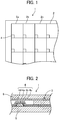
- a plurality of display areas 2 are arranged in a matrix in the display device 1.
- the display areas 2 fall into three types: red emission regions 2a emitting red light, green emission regions 2b emitting green light, and blue emission regions 2c emitting blue light. These three emission regions 2a, 2b, and 2c are for example arranged in a row direction to form a set constituting one pixel for color display.
- a light emitting device 3 is formed in each of the emission regions 2a, 2b, and 2c.
- the layer structure of the light emitting device 3 will be described below.
- a thin film transistor (TFT) 4 is connected to each light emitting device 3.
- the light emitting devices 3 are top emission devices.
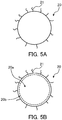
- the thin film transistor 4 illustrated in FIG. 2 is an n-ch TFT, which is built in such a manner that a gate electrode 4a, a channel layer 4b, a gate insulating film (not shown), a drain electrode 4c, a source electrode 4d, etc. are stacked on a substrate 5.
- the channel layer 4b is formed from an N-type semiconductor; preferably, an oxide semiconductor is used. However, the material of the layer is not limited to this.
- an In-Ga-Zn-O-based semiconductor is preferably used.
- An In-Ga-Zn-O-based semiconductor has high mobility and causes low leakage current, and thus can be suitably used in the thin film transistor.
- Poly-Si can be preferably used.
- the thin film transistor 4 depicted in FIG. 2 has a top-contact bottom-gate configuration; alternatively, the thin film transistor 4 may have a bottom-contact bottom-gate configuration.
- the source electrode 4d is connected to a power supply line, and the drain electrode 4c is connected to the light emitting device 3.
- the thin film transistor 4 may have a top-gate configuration depicted in FIG. 3 .
- the channel layer 4b is formed on the substrate 5, and the surface of the channel layer 4 is covered with the gate insulating film 4e.
- the gate electrode 4a is formed on the surface of the gate insulating film 4e.
- the surface of the gate electrode 4a is covered with an insulating film 4f.
- a plurality of through holes extending through the gate insulating film 4e and the insulating film 4f to reach the channel layer 4b, and the drain electrode 4c and the source electrode 4d are formed in the respective through holes.
- the surfaces of the drain electrode 4c and the source electrode 4d are covered with a protective film 7.
- a transparent electrode connected to the drain electrode 4c and the source electrode 4d is formed on the surface of the protective film 7.
- the transparent electrode 8 depicted in FIG. 3 is connected to the drain electrode 4c.
- the channel layer 4b of the thin film transistor 4 shown in FIG. 3 is an N-type semiconductor, and an oxide semiconductor is preferably used.
- an oxide semiconductor is preferably used.
- an In-Ga-Zn-O-based semiconductor is preferably used.
- the display device 1 has a structure in which the thin film transistor 4 and the light emitting device 3 are interposed between a pair of substrates 5 and 6, and, although not shown, sealing resin is provided in a frame pattern between the substrates 5 and 6 so that the substrates 5 and 6 are connected with the sealing resin therebetween.
- FIG. 4A is a cross-sectional view of a light emitting device of Embodiment 1
- FIG. 4B is an energy level diagram of each layer in a display device of Embodiment 1.
- the light emitting device 3 is configured to have a substrate 10, a cathode 15 formed on the substrate, an electron transport layer (ETL) 14 formed on the cathode 15, an emitting layer (EML) 13 formed on the electron transport layer 14, a hole transport layer (HTL) 12 formed on the emitting layer 13, and an anode 11 formed on the hole transport layer 12.
- ETL electron transport layer
- EML emitting layer
- HTL hole transport layer
- FIG. 4B shows the energy level models of the hole transport layer 12, the emitting layer 13, and the electron transport layer 14.
- holes transported through the hole transport layer 12 are injected from the HOMO level of the hole transport layer 12 into the HOMO level of the emitting layer 13.
- electrons transported through the electron transport layer 14 are injected from the LUMO level of the electron transport layer 14 into the LUMO level of the emitting layer 13. The holes and electrons are recombined in the emitting layer 13, which promotes quantum dots in the emitting layer 13 to the excited state, thus light emission from the excited quantum dots can be achieved.
- the emitting layer 13 is formed of an inorganic layer containing quantum dots.
- quantum dots in this embodiment are nanoparticles having a particle diameter of around several nanometers to several tens of nanometers; however, the structure and the material of the quantum dots are not limited to those.
- quantum dots are formed from CdS, CdSe, ZnS, ZnSe, ZnSeS, ZnTe, ZnTeS, InP, (Zn)AgInS 2 , (Zn)CuInS 2 , etc. Because of the toxicity of Cd, the use of Cd is restricted in many countries; thus, quantum dots are preferably free of Cd.
- organic ligands 21 are preferably placed on the surface of a quantum dot 20. This can inhibit aggregation of quantum dots 20, resulting in the target optical properties.
- the ligands available for the reaction are not particularly limited; for example, the following ligands can be given as typical examples.
- Aliphatic primary amines oleylamine: C 18 H 35 NH 2 , stearyl(octadecyl)amine: C 18 H 37 NH 2 , dodecyl(lauryl)amine: C 12 H 25 NH 2 , decylamine: C 10 H 21 NH 2 , octylamine: C 8 H 17 NH 2
- Aliphatic acids oleic acid: C 17 H 33 COOH, stearic acid: C 17 H 35 COOH, palmitic acid: C 15 H 31 COOH, myristic acid: C 13 H 27 COOH, lauric (dodecanoic) acid: C 11 H 23 COOH, decanoic acid: C 9 H 19 COOH, octanoic acid: C 7 H 15 COOH
- Thiols octadecanethiol: C 18 H 37 SH, hexadecanethiol: C 16 H 33 SH, tetradecanethiol: C
- a quantum dot 20 depicted in FIG. 5B has a core-shell structure having a core 20a and a shell 20b covering the surface of the core 20a. As shown in FIG. 5B , many organic ligands 21 are preferably placed on the surface of the quantum dot 20.
- the core 20a of the quantum dot 20 shown in FIG. 5B is the nanoparticle shown in FIG. 5A . Accordingly, the core 20a is formed for example from the materials listed above.
- the shell 20b is formed from, for example, zinc sulfide (ZnS); however, the material of the shell 20b is not limited to this. As with the core 20a, the shell 20b is preferably free of cadmium (Cd).
- the shell 20b may be in a condition of being a solid solution on the surface of the core 20a.
- the boundary between the core 20a and the shell 20b is indicated by a dotted line, and this means that the boundary between the core 20a and the shell 20b may or may not be identified by an analysis.
- the emitting layer 13 may be formed from the above-mentioned quantum dots alone; alternatively, the emitting layer 13 may contain the quantum dots and another luminescent material other than the quantum dots. Further, the emitting layer 13 may be formed by applying quantum dots dissolved in a solvent, for example, by the inkjet process. Here, a slight amount of the solvent component may be left in the emitting layer 13.
- Red quantum dots emitting red light are contained in the emitting layer 13 of the light emitting devices 3 formed in the red emission regions 2a depicted in FIG. 1 . Further, green quantum dots emitting green light are contained in the emitting layer 13 in the light emitting devices 3 formed in the green emission regions 2b depicted in FIG. 1 . Further, blue quantum dots emitting blue light are contained in the emitting layer 13 in the light emitting devices 3 formed in the blue emission regions 2c depicted in FIG. 1 .
- the wavelength of blue emission is preferably around 450 nm.
- health risks can be reduced by adjustments such that light of a wavelength shorter than 450 nm is not emitted can.
- the emitting layer 13 can be formed by an existing thin film formation method such as the inkjet process and vacuum deposition mentioned above.
- the hole transport layer 12 is made from an inorganic material or an organic material having hole transporting functions.
- the hole transport layer 12 is preferably made from an inorganic material, for example, is preferably formed from an inorganic oxide such as NiO or WO 3 .
- the hole transport layer 12 is preferably formed from nanoparticles of NiO.
- Al 2 O 3 or the like may be mixed in NiO.
- a metal oxide may be doped with Li, Mg, Al, etc.
- the hole transport layer 12 may be of an inorganic material other than inorganic oxides.
- the hole transport layer 12 can be formed by a printing process such as the inkjet process, or may be formed by an existing thin film technique such as vacuum deposition.
- the electron transport layer 14 is made from an inorganic material or an organic material having electron transporting functions.
- the electron transport layer 14 is preferably made from an inorganic material, for example, is preferably formed from an inorganic oxide such as ZnOx, Ti-O, Sn-O, V-Ox, or Mo-O. Two or more of these materials may be selected as materials.
- the electron transport layer 14 is preferably formed from nanoparticles of ZnOx.
- a metal oxide may be doped with Li, Mg, Al, Mn, etc.
- the electron transport layer 14 may be of an inorganic material (for example, CsPbBr 3 etc.) other than inorganic oxides.
- X is, but not limited to, around 0.8 to 1.2.
- the electron transport layer 14 can be formed by applying a solvent containing nanoparticles by a printing process such as the inkjet process, or may be formed by an existing thin film technique such as vacuum deposition.
- the material for forming the anode 11 is preferably for example, but not limited to, a metal such as Au or Ag, a conductive transparent material such as CuISnO 2 or ZnOx, or a compound oxide of indium-tin (ITO). Of those, the anode 11 is preferably formed from ITO.
- the anode 11 can be formed as a thin film of the electrode material on the substrate 10 by a method such as vapor deposition or sputtering.
- the anode 11 since a structure in which light is given off from the anode 11 side is used, the anode 11 needs to be transparent, and is preferably a thin metal film of Ag etc. that is excellent in transparency, or one of the metal oxides excellent in transparency that are mentioned above.
- a compound oxide of indium-tin (ITO), a metal, an alloy, an electrically conductive compound, or a mixture of those can be used as an electrode material of the cathode 15; however, the material of the cathode 15 is not limited to those.
- the cathode 15 is formed from ITO.
- the cathode 15 is, for example, formed on an opaque metal layer formed on the substrate 10.
- the light emitting device 3 is obtained as a top emission device.
- the cathode 15 can be formed as a thin film of the electrode material by a method such as vapor deposition or sputtering.
- the substrate 10 can be formed of, for example, glass or plastic; however, the material of the substrate 10 is not limited to these. Specifically, the substrate 10 is formed of, for example, glass, quartz, or a transparent resin film.
- the substrate 10 may either be a rigid substrate or a flexible substrate; when a flexible substrate is used, a flexible device can be obtained.
- the material of the transparent film include, for example, polyethylene terephthalate (PET), polyethylene naphthalate (PEN), polyester, polyethylene, polypropylene, cellophane, cellulose diacetate, and cellulose triacetate (TAC).
- the display device 1 in FIG. 2 using flexible substrates for the substrates 5 and 6, the display device 1 can be flexible. Note that the substrates 5 and 6 can also be formed using a similar material to that of the substrate 10. The substrate 5 can also serve as the substrate 10.
- all the layers from the cathode 15 to the anode 11, that is, all the cathode 15, the electron transport layer 14, the emitting layer 13, the hole transport layer 12, and the anode 11 can each be formed of an inorganic layer. Forming all the layers from inorganic layers allow all the layers to be formed using the same coating/drying apparatuses, etc. and facilitates the production process. Further, the high-low relationships of the HOMO levels of the anode 11, the hole transport layer 12, and the emitting layer 13 can be optimized; the high-low relationships of the LUMO levels of the cathode 15, the electron transport layer 14, and the emitting layer 13 can be optimized. This improves the carrier balance as compared with the case of using organic compounds.
- a hole injection layer and an electron injection layer are not formed separately from the transport layers, thus the number of the layers can be reduced.
- the transport layers also serve as injection layers.
- a hole injection layer and an electron injection layer made of an inorganic material may be interposed between the electrodes and the transport layers.
- FIG. 6A is a cross-sectional view of a light emitting device of Embodiment 2.
- the cathode 15, the electron transport layer 14, the emitting layer 13, the hole transport layer 12, a hole injection layer (HIL) 16, and the anode 11 are stacked in this order on the substrate 10.
- the hole injection layer 16 is placed between the anode 11 and the hole transport layer 12.
- FIG. 6B is a cross-sectional view of a light emitting device of Embodiment 3.
- the cathode 15, an electron injection layer (EIL) 18, the electron transport layer 14, the emitting layer 13, the hole transport layer 12, and the anode 11 are stacked in this order on the substrate 10.
- the electron injection layer 18 is placed between the electron transport layer 14 and the cathode 15.
- FIG. 6C is a cross-sectional view of a light emitting device of Embodiment 4.
- the cathode 15, the electron injection layer 18, the electron transport layer 14, the emitting layer 13, the hole transport layer 12, the hole injection layer 16, and the anode 11 are stacked in this order on the substrate 10.
- the hole injection layer 16 is placed between the anode 11 and the hole transport layer 12, and in addition, the electron injection layer 18 is placed between the electron transport layer 14 and the cathode 15.
- the material of the hole injection layer 16 and the electron injection layer 18 may be either an inorganic material or an organic material. Forming the hole injection layer 16 and the electron injection layer 18 from inorganic layers is preferred because all the layers from the anode 11 to the cathode 15 can each be formed of an inorganic layer. However, the material of the injection layers is not limited to this. The material of the hole injection layer 16 and the electron injection layer 18 is selected from various kinds of materials depending on the energy level models.
- the layer between the cathode 15 and the light emitting layer 13 is preferably a layer serving as the electron transport layer 14, the electron injection layer 18, or both the electron injection layer and the electron transport layer; or a layer in which the electron transport layer 14 and the electron injection layer 18 are stacked.
- the layer between the anode 11 and the emitting layer 13 is preferably a layer serving as the hole transport layer 12, the hole injection layer 16, or both the hole injection layer and the hole transport layer; or a layer in which the hole transport layer 12 and the hole injection layer 16 are stacked.
- the thin film transistor 4 has, for example, a bottom-gate configuration, and the drain electrode 4c is connected to the cathode 15 of the light emitting device 3.
- the drain electrode 4c can be made to serve as the cathode 15 without forming the cathode 15 superposed on the drain electrode 4c. This allows the light emitting device 3 to be suitably connected with the thin film transistor 4 and the ground line.
- the hole transport layer 12, the emitting layer 13, and the electron transport layer 14 can all be inorganic layers formed from nanoparticles.
- each layer can be formed by printing by the inkjet process or the like, thus the layers can be formed easily and formed to be uniform in thickness. This can effectively improve emission efficiency.
- the energy level diagram presented in FIG. 7A is obtained, and the energy level of the shell would be as a barrier to the recombination of holes and electrons.
- a quantum dot of which surface is not covered with a shell (the surface of the core is exposed, or the material forming the quantum dot is uniform from the center of the quantum dot to the surface thereof) as shown in FIG. 7B is preferably used.
- the organic ligands 21 are preferably placed on the surface of each quantum dot 20 as illustrated in FIG. 5A .
- the light emitting device 3 may be configured to have the substrate 10, the anode 11 formed on the substrate, the hole transport layer (HTL) 12 formed on the anode 11, the emitting layer (EML) 13 formed on the hole transport layer 12, the electron transport layer (ETL) 14 formed on the emitting layer 13, and the cathode 15 formed on the electron transport layer 14.
- HTL hole transport layer
- EML emitting layer
- ETL electron transport layer
- the cathode 15 forms a second electrode. Since the light emitting device 3 of this embodiment is a top emission device, the cathode 15 is preferably formed of a very thin transparent material such as Ag, and the anode 11 is preferably made of ITO, for example, on an opaque metal layer. This allows light to be reflected at the anode 11 and light to be given off from the surface side on the cathode 15 side (opposite to the thin film transistor side).
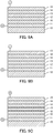
- FIG. 9A is a cross-sectional view of a light emitting device according to a different embodiment from FIG. 8A .
- the anode 11, the hole injection layer (HIL) 16, the hole transport layer 12, the emitting layer 13, the electron transport layer 14, and the cathode 15 are stacked in this order on the substrate 10.
- the hole injection layer 16 is placed between the anode 11 and the hole transport layer 12.
- FIG. 9B is a cross-sectional view of a light emitting device according to a different embodiment from FIG. 8A .
- the anode 11, the hole transport layer 12, the emitting layer 13, the electron transport layer 14, the electron injection layer (EIL) 18, and the cathode 15 are stacked in this order on the substrate 10.
- the electron injection layer 18 is placed between the electron transport layer 14 and the cathode 15.
- FIG. 9C is a cross-sectional view of a light emitting device according to Embodiment 4.
- the anode 11, the hole injection layer 16, the hole transport layer 12, the emitting layer 13, the electron transport layer 14, the electron injection layer 18, and the cathode 15 are stacked in this order on the substrate 10.
- the hole injection layer 16 is placed between the anode 11 and the hole transport layer 12, and in addition, the electron injection layer 18 is placed between the electron transport layer 14 and the cathode 15.
- the energy level diagram presented in FIG. 10A is obtained, and the energy level of the shell would be as a barrier to the recombination of holes and electrons. Accordingly, using quantum dots in which the surface of the core is not covered with a shell as depicted in FIG. 10B eliminates the energy barrier to the recombination of hole and electrons, and allows holes and electrons to be efficiently recombined, thus the light emission efficiency can be improved.
- the organic ligands 21 are preferably placed on the surface of each quantum dot 20 as illustrated in FIG. 5A .
- the light emitting devices of the embodiments shown in FIG. 8A to FIG. 9C are conventional EL devices, and the light emitting devices of the embodiments in FIGS. 4A and 4B and FIGS. 6A to 6C have layered structures opposite to that of the Conventional EL devices.
- the thin film transistor is preferably a p-ch TFT; accordingly, the channel layer is preferably formed from a P-type semiconductor.
- At least one of the layer between the cathode 15 and the emitting layer 13, the emitting layer 13, and the layer between the emitting layer 13 and the anode 11 can be formed by the inkjet process.
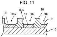
- a mask 30 is placed on the substrate 10, and an inorganic layer 31 is printed in a plurality of application regions 30a provided in the mask 30 by the inkjet process.
- the surfaces of the sidewalls 30b of the rises of the mask 30 are, for example, subjected to fluorination to impart water repellency to the sidewalls 30b. This can reduce the affinity of the surface of the sidewalls 30b for ink and prevents defects such as dents in the surface of the printed inorganic layer 31, and thus can increase the flatness of the surface of the inorganic layer 31.
- This embodiment involves top emission devices, and can improve the carrier balance in the inverted EL light emitting devices 3 depicted in FIGS. 4A and 4B and FIGS. 6A to 6C .
- the layers between the cathode 15 and the light emitting layer 13 (the electron transport layer 14 or both the electron transport layer 14 and the electron injection layer 18) and the light emitting layer 13 can be formed by coating.
- the layers between the light emitting layer 13 and the anode 11 can be formed by vapor deposition or coating. This can facilitate the production process of the light emitting devices.
- the display device 1 depicted in FIG. 1 is an example, and the arrangement of the red emission regions 2a, the green emission regions 2b, and the blue emission regions 2c may be different from that in FIG. 1 . Further, of the red emission regions 2a, the green emission regions 2b, and the blue emission regions 2c, only the emission regions of one color or the emission regions of two colors may be included in the display device.
- the quantum dots can be used to build either a point light source or a surface light source, and a curved light source or a flexible product may also be obtained by selecting a suitable substrate.
- distinctive products such as lightings producing a mixture of colors comparable to that of sunlight which has been hardly obtained, lightings producing light easy on the eyes, and lightings optimized for plant factories can be developed.
- display devices using quantum dots provide a high degree of flexibility in the design; for example, the devices can be formed to be thin, lightweight, and curved. Further, the devices can produce natural light not dazzling in the eyes that produces less shadows. In addition, the devices consume less power and have a long life. For example, display devices using quantum dots of this embodiment are superior to organic EL display devices in terms of color rendering properties, emission properties, product life, and product price.
- a display device using quantum dots of this embodiment can be used as a PL emitter as well as an EL emitter. Further, for a display device using quantum dots, a hybrid light emitting device in which an EL emitter and a PL emitter are stacked can be obtained. For example, a PL emitter is superposed on a surface of an EL emitter, and the emission wavelength of the light emitted by excited quantum dots in the EL emitter can be changed using the quantum dots contained in the PL emitter.
- the EL emitter is a light emitting device having a layered structure described above, and the PL emitter is, for example, a sheet-like wavelength converting member in which a plurality of quantum dots are dispersed in a resin. Such a hybrid structure can be obtained with the use of quantum dots.
- the inkjet printing process, the spin coating process, or the dispensing process is preferably used as a method for applying the quantum dots.
- Table 1 shows that IPA and propylene glycol were not preferred as the solvent for zinc oxide nanoparticles, and another solvent had to be used.
- the solvents corresponding to the "+" signs in the "drop” column shown in Table 1 can be appropriately used; however, hydrophilic solvents are preferred.
- a hydrophilic solvent an alcohol-based solvent can be used.
- EPDM ethylene propylene diene monomer rubber
- the shell thickness was, but not limited to, 0.1 nm or more and 4.0 nm or less, preferably 0.5 nm or more and 3.5 nm or less, more preferably 1.0 nm or more and 3.0 nm or less, still more preferably 1.3 nm or more and 2.5 nm or less.
- the quantum dot thickness was, but not limited to, 5 nm or more and 50 nm or less, preferably 10 nm or more and 45 nm or less, more preferably 15 nm or more and 40 nm or less, still more preferably 20 nm or more and 40 nm or less, yet more preferably 25 nm or more and 40 nm or less.
- Cd-based green quantum dots were subjected to PYS measurements.
- the circle marks represent experimental data of the quantum dots each constituted by a core alone in Example 1
- the square marks represent experimental data of the quantum dots constituted by a core coated with a shell in Example 2.
- the photo-electron yield spectroscopy can measure the ionization potential.
- the measurement can be performed using a system named AC-2/AC-3 manufactured by RIKEN KEIKI CO., LTD.
- Example 2 As shown in FIG. 13 , the energy of the rising edge in Example 1 was found to be different from that in Example 2. The energy rose at approximately 6.1 eV in Example 1, and the energy rose at approximately 7.1 eV in Example 2.
- FIG. 14 shows the PYS measurement results of the Cd-based green quantum dots with different shell thicknesses in Example 3 and Example 4.
- the shell thickness was larger in Example 4 than in Example 3.
- the energy of the rising edge in Example 3 was found to be different from that in Example 4.
- FIG. 15 is an energy level diagram of each layer in the light emitting device used in an experiment.
- FIG. 16 is a graph illustrating the relationship between the current value and the EQE of an EL emitter and a PL emitter using red quantum dots; Further, FIG. 17 shows plots illustrating the relationship between the current value and the EQE of an EL emitter and a PL emitter using red quantum dots; and a plot illustrating the relationship between the current value and the EQE of an EL emitter using blue quantum dots.
- the shell thicknesses in Example 5 and Example 6 in FIG. 16 were different. The shell thickness was larger in Example 5 than in Example 6. Further, in FIG. 17 , the shell thickness was largest in Example 7, and the shell thickness was smaller in Example 8 and Example 9 in this order.
- the EQE increased to the point around 20 mA.
- the EQE increased even when the current value was 20 mA or more.
- a larger shell thickness resulted in a larger increase in the EQE.
- FIG. 18 presents a graph illustrating the energy band gap Eg of each layer in the light emitting device used in an experiment, the energy E CB at the bottom of the conduction band, and the energy E CB at the top of the conduction band, and an energy level diagram of the layers.
- ZnO X (Li) was used as L1 or L2 in FIG. 18 .
- Li may or may not be added.
- X is, but not limited to, around 0.8 to 1.2.
- FIG. 18 it was found that use of ZnO X (Li) as ZnO X used for the electron injection layer (ETL) and the electron transport layer increased the band gap.
- ZnO X (Li) is presumed to have an effect of reducing the particle diameter.
- PVK shown in FIG. 18 corresponds to a hole injection layer
- B1, B2, G(H), G(I3), and R(F) correspond to emitting layers (EL layers);
- ZnO X , L2, and L4 correspond to electron injection layers.
- B1 or B2 is used for the emitting layer
- ZnO X can be used for the electron injection layer; however, it was found that when G(H), G(I3), or R(F) was used for the emitting layer, L2 or L4 was preferably used for the electron injection layer.
- L2 and L4 are ZnO X (Li).
- ZnO X (Li) can be, but not exclusively, prepared by stirring a zinc acetate-ethanol solution at a predetermined temperature for a predetermined time, and then mixing and stirring a LiOH ⁇ 4H 2 O-ethanol solution, followed by centrifugal separation, cleaning, etc.
- FIG. 19 to FIG. 21 show the UV (band gap), the PL spectra, and the PYS data of ZnO X (Li) and ZnO X (K) used for the electron injection layer (ETL).
- ZnO X (K) was produced using KOH catalytically and was not doped with K or Li.
- ZnO X (Li) and ZnO X (K) were found to show differences in the UV data and the PL data.
- the PYS data of ZnO X (Li) and ZnO X (K) hardly differed, and the rising edge energies were almost the same.
- ZnO X of which band gap is controlled by selecting from different particle diameters to be used for an electron injection/transport layer of an EL device using quantum dots, and doped ZnO X for which defects are controlled and the band gap is controlled by adding doping species can be proposed.
- hole blocking functions are preferably added by interposing a thick insulating layer between the EL layer and the electron injection layer or integrating ZnOx with molecules thereby adjusting the balance.
- the integrated layer involves the integration of, for example, ZnO X with T2T (2,4,6-tris(biphenyl-3-yl)-1,3,5-triazine).
- X is, but not limited to, around 0.8 to 1.2.
- ZnO X is known to have functions suitable for use in not only the electron injection/transport layer but also in a hole injection/transportation layer by performing ozone treatment or the like. Specifically, performing ozone treatment on ZnOx was found to improve the hole transporting performance.
- a light emitting device containing quantum dots can be used for a display device, and excellent emission properties can be obtained.
Landscapes
- Chemical & Material Sciences (AREA)
- Engineering & Computer Science (AREA)
- Physics & Mathematics (AREA)
- Inorganic Chemistry (AREA)
- Materials Engineering (AREA)
- Organic Chemistry (AREA)
- Optics & Photonics (AREA)
- Nanotechnology (AREA)
- Crystallography & Structural Chemistry (AREA)
- Microelectronics & Electronic Packaging (AREA)
- Geometry (AREA)
- General Physics & Mathematics (AREA)
- Theoretical Computer Science (AREA)
- Manufacturing & Machinery (AREA)
- Electroluminescent Light Sources (AREA)
- Devices For Indicating Variable Information By Combining Individual Elements (AREA)
- Optical Filters (AREA)
Abstract
Description
- The present invention relates to a display device using quantum dots.
-
JP 2017-045650 A - An organic EL device has a structure in which an anode, a hole injection layer, a hole transport layer, an emitting layer, an electron transport layer, an electron injection layer, and a cathode are stacked on a substrate. Such an organic EL device is formed from an organic compound and emits light from excitons formed by the recombination of electrons and holes injected into the organic compound.
- PTL 1:
JP 2017-045650 A - In recent years, light emitting devices using quantum dots are being developed. Quantum dots are nanoparticles made of around several hundreds to several thousands of atoms, each having a particle diameter of around several nanometers to several tens of nanometers. Quantum dots are also referred to as fluorescent nanoparticles, semiconductor nanoparticles, or nanocrystals. The emission wavelength of quantum dots may be variously changed depending on the particle diameter and the composition of the nanoparticles. As with an organic EL device, a light emitting device using quantum dots makes it possible to obtain a thinner device and surface emission.
- However, the layered structure of top emission light emitting devices using quantum dots, and the structure of display devices using such light emitting devices have not yet been established.
- The present invention is made in consideration of the above, and seeks to provide a display device having a light emitting device that includes quantum dots.
- A display device according to the present invention includes a display area. The display area has a light emitting device in which a first electrode, a layer between the first electrode and an emitting layer, the emitting layer, a layer between the emitting layer and a second electrode, and the second electrode are stacked in this order on a substrate. The emitting layer is formed of an inorganic layer containing quantum dots, and the light emitting device is a top emission device.
- In an aspect of the present invention, a thin film transistor connected to the light emitting device is preferably an n-ch TFT.
- In another aspect of the present invention, an oxide semiconductor of the thin film transistor is preferably an In-Ga-Zn-O-based semiconductor.
- In yet another aspect of the present invention, the display device is preferably flexible.
- In yet another aspect of the present invention, the quantum dots preferably have a structure in which a surface of a core is not covered by a shell.
- In yet another aspect of the present invention, at least one of the layer between the first electrode and the emitting layer, the emitting layer, and the layer between the emitting layer and the second electrode is formed by an inkjet process.
- In yet another aspect of the present invention, the layer between the first electrode and the emitting layer, and the emitting layer are preferably formed by coating; and the layer between the emitting layer and the second electrode is preferably formed by vapor deposition or coating.
- In a display device of the present invention, the layered structure of light emitting devices containing quantum dots, used in a display device can be optimized. Further, in the present invention, all the layers from the cathode to the anode can be formed of inorganic layers.
- In the accompanying drawings:
-
FIG. 1 is a partial plan view of a display device according to one embodiment; -
FIG. 2 is a partial enlarged cross-sectional view illustrating one of display areas of the display device depicted inFIG. 1 that is enlarged; -
FIG. 3 is a cross-sectional view illustrating the structure of a thin film transistor different from one inFIG. 2 ; -
FIG. 4A is a cross-sectional view of a light emitting device ofEmbodiment 1, andFIG. 4B is an energy level diagram of each layer in a display device ofEmbodiment 1; -
FIG. 5 is a schematic view of a quantum dot according to one embodiment; -
FIGS. 6A to 6C are cross-sectional views each illustrating a light emitting device according to an embodiment different from that inFIG. 1 ; -
FIG. 7A is an energy level diagram in the case of using quantum dots having a core-shell structure, andFIG. 7B is an energy level diagram in the case of using quantum dots having a structure in which a core is not covered by a shell; -
FIG. 8A is a cross-sectional view of a light emitting device different from one inFIG. 4 , andFIG. 8B is an energy level diagram of each layer in the light emitting device ofFIG. 8A ; -
FIGS. 9A to 9C are cross-sectional views each illustrating a light emitting device according to an embodiment different from that inFIG. 8 ; -
FIG. 10A is an energy level diagram in the case of using quantum dots having a core-shell structure, andFIG. 10B is an energy level diagram in the case of using quantum dots having a structure in which a core is not covered by a shell; -
FIG. 11 is a schematic view illustrating a step of forming an inorganic layer by the inkjet process; -
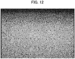
FIG. 12 is a photograph showing an application in Examples; -
FIG. 13 shows PYS measurement data of Cd-based green quantum dots; -
FIG. 14 shows PYS measurement data; -
FIG. 15 is an energy level diagram of each layer in the light emitting device used in an experiment; -
FIG. 16 is a graph illustrating the relationship between the current value and the EQE of an EL emitter and a PL emitter using green quantum dots; -
FIG. 17 shows plots illustrating the relationship between the current value and the EQE of an EL emitter and a PL emitter using red quantum dots; and a plot illustrating the relationship between the current value and the EQE of an EL emitter using blue quantum dots; -
FIG. 18 presents a graph illustrating the energy band gap Eg of each layer in the light emitting device used in an experiment, the energy ECB at the bottom of the conduction band, and the energy ECB at the top of the conduction band, and an energy level diagram of the layers; -
FIG. 19 shows the UV data of ZnOX(Li) and ZnOX(K) used in an electron transport layer (ETL); -
FIG. 20 shows the PL data of ZnOX(Li) and ZnOX(K) used in an electron transport layer (ETL); and -
FIG. 21 shows the PYS data of ZnOX(Li) and ZnOX(K) used in an electron transport layer (ETL). - Embodiments of the present invention (hereinafter simply referred to as "embodiments") will now be described in detail. Note that the present invention is not limited to the following embodiments, and various modifications may be made without departing from the spirit of the present invention.
- As illustrated in
FIG. 1 , a plurality ofdisplay areas 2 are arranged in a matrix in thedisplay device 1. Thedisplay areas 2 fall into three types:red emission regions 2a emitting red light,green emission regions 2b emitting green light, andblue emission regions 2c emitting blue light. These threeemission regions - In each of the
emission regions light emitting device 3 is formed. The layer structure of thelight emitting device 3 will be described below. A thin film transistor (TFT) 4 is connected to each light emittingdevice 3. Thelight emitting devices 3 are top emission devices. - The
thin film transistor 4 illustrated inFIG. 2 is an n-ch TFT, which is built in such a manner that agate electrode 4a, achannel layer 4b, a gate insulating film (not shown), adrain electrode 4c, asource electrode 4d, etc. are stacked on asubstrate 5. Thechannel layer 4b is formed from an N-type semiconductor; preferably, an oxide semiconductor is used. However, the material of the layer is not limited to this. As the oxide semiconductor, an In-Ga-Zn-O-based semiconductor is preferably used. An In-Ga-Zn-O-based semiconductor has high mobility and causes low leakage current, and thus can be suitably used in the thin film transistor. Alternatively, Poly-Si can be preferably used. Thethin film transistor 4 depicted inFIG. 2 has a top-contact bottom-gate configuration; alternatively, thethin film transistor 4 may have a bottom-contact bottom-gate configuration. - The
source electrode 4d is connected to a power supply line, and thedrain electrode 4c is connected to thelight emitting device 3. - Further, the
thin film transistor 4 may have a top-gate configuration depicted inFIG. 3 . As illustrated inFIG. 3 , thechannel layer 4b is formed on thesubstrate 5, and the surface of thechannel layer 4 is covered with the gate insulating film 4e. Thegate electrode 4a is formed on the surface of the gate insulating film 4e. As illustrated inFIG. 3 , the surface of thegate electrode 4a is covered with an insulatingfilm 4f. Further, a plurality of through holes extending through the gate insulating film 4e and the insulatingfilm 4f to reach thechannel layer 4b, and thedrain electrode 4c and thesource electrode 4d are formed in the respective through holes. Further, the surfaces of thedrain electrode 4c and thesource electrode 4d are covered with aprotective film 7. Further, a transparent electrode connected to thedrain electrode 4c and thesource electrode 4d is formed on the surface of theprotective film 7. Thetransparent electrode 8 depicted inFIG. 3 is connected to thedrain electrode 4c. - The
channel layer 4b of thethin film transistor 4 shown inFIG. 3 is an N-type semiconductor, and an oxide semiconductor is preferably used. As the oxide semiconductor, an In-Ga-Zn-O-based semiconductor is preferably used. - As illustrated in
FIG. 2 , thedisplay device 1 has a structure in which thethin film transistor 4 and thelight emitting device 3 are interposed between a pair ofsubstrates substrates substrates - Hereinafter, the structure of the
light emitting device 3 will be described.FIG. 4A is a cross-sectional view of a light emitting device ofEmbodiment 1, andFIG. 4B is an energy level diagram of each layer in a display device ofEmbodiment 1. - As shown in
FIG. 4A , thelight emitting device 3 is configured to have asubstrate 10, acathode 15 formed on the substrate, an electron transport layer (ETL) 14 formed on thecathode 15, an emitting layer (EML) 13 formed on theelectron transport layer 14, a hole transport layer (HTL) 12 formed on the emittinglayer 13, and ananode 11 formed on thehole transport layer 12. - When a voltage is applied to between the electrodes of the
light emitting device 3 in this embodiment, holes are injected from theanode 11, and electrons are injected from thecathode 15.FIG. 4B shows the energy level models of thehole transport layer 12, the emittinglayer 13, and theelectron transport layer 14. As shown inFIG. 4B , holes transported through thehole transport layer 12 are injected from the HOMO level of thehole transport layer 12 into the HOMO level of the emittinglayer 13. On the other hand, electrons transported through theelectron transport layer 14 are injected from the LUMO level of theelectron transport layer 14 into the LUMO level of the emittinglayer 13. The holes and electrons are recombined in the emittinglayer 13, which promotes quantum dots in the emittinglayer 13 to the excited state, thus light emission from the excited quantum dots can be achieved. - In this embodiment, the emitting
layer 13 is formed of an inorganic layer containing quantum dots. - For example, quantum dots in this embodiment are nanoparticles having a particle diameter of around several nanometers to several tens of nanometers; however, the structure and the material of the quantum dots are not limited to those.
- For example, quantum dots are formed from CdS, CdSe, ZnS, ZnSe, ZnSeS, ZnTe, ZnTeS, InP, (Zn)AgInS2, (Zn)CuInS2, etc. Because of the toxicity of Cd, the use of Cd is restricted in many countries; thus, quantum dots are preferably free of Cd.
- As shown in
FIG. 5A , manyorganic ligands 21 are preferably placed on the surface of aquantum dot 20. This can inhibit aggregation ofquantum dots 20, resulting in the target optical properties. The ligands available for the reaction are not particularly limited; for example, the following ligands can be given as typical examples.
Aliphatic primary amines: oleylamine: C18H35NH2, stearyl(octadecyl)amine: C18H37NH2, dodecyl(lauryl)amine: C12H25NH2, decylamine: C10H21NH2, octylamine: C8H17NH2
Aliphatic acids: oleic acid: C17H33COOH, stearic acid: C17H35COOH, palmitic acid: C15H31COOH, myristic acid: C13H27COOH, lauric (dodecanoic) acid: C11H23COOH, decanoic acid: C9H19COOH, octanoic acid: C7H15COOH Thiols: octadecanethiol: C18H37SH, hexadecanethiol: C16H33SH, tetradecanethiol: C14H29SH, dodecanethiol: C12H25SH, decanethiol: C10H21SH, octanethiol: C8H17SH
Phosphines: trioctylphosphine: (C8H17)3P, triphenylphosphine: (C6H5)3P, tributylphosphine: (C4H9)3P
Phosphine oxides: trioctylphosphine oxide: (C8H17)3P=O, triphenylphosphine oxide: (C6H5)3P=O, tributylphosphine oxide: (C4H9)3P=O - A
quantum dot 20 depicted inFIG. 5B has a core-shell structure having acore 20a and ashell 20b covering the surface of thecore 20a. As shown inFIG. 5B , manyorganic ligands 21 are preferably placed on the surface of thequantum dot 20. The core 20a of thequantum dot 20 shown inFIG. 5B is the nanoparticle shown inFIG. 5A . Accordingly, thecore 20a is formed for example from the materials listed above. Theshell 20b is formed from, for example, zinc sulfide (ZnS); however, the material of theshell 20b is not limited to this. As with thecore 20a, theshell 20b is preferably free of cadmium (Cd). - The
shell 20b may be in a condition of being a solid solution on the surface of thecore 20a. InFIG. 5B , the boundary between the core 20a and theshell 20b is indicated by a dotted line, and this means that the boundary between the core 20a and theshell 20b may or may not be identified by an analysis. - The emitting
layer 13 may be formed from the above-mentioned quantum dots alone; alternatively, the emittinglayer 13 may contain the quantum dots and another luminescent material other than the quantum dots. Further, the emittinglayer 13 may be formed by applying quantum dots dissolved in a solvent, for example, by the inkjet process. Here, a slight amount of the solvent component may be left in the emittinglayer 13. - Red quantum dots emitting red light are contained in the emitting
layer 13 of thelight emitting devices 3 formed in thered emission regions 2a depicted inFIG. 1 . Further, green quantum dots emitting green light are contained in the emittinglayer 13 in thelight emitting devices 3 formed in thegreen emission regions 2b depicted inFIG. 1 . Further, blue quantum dots emitting blue light are contained in the emittinglayer 13 in thelight emitting devices 3 formed in theblue emission regions 2c depicted inFIG. 1 . - Note that the wavelength of blue emission is preferably around 450 nm. Thus, health risks can be reduced by adjustments such that light of a wavelength shorter than 450 nm is not emitted can.
- The emitting
layer 13 can be formed by an existing thin film formation method such as the inkjet process and vacuum deposition mentioned above. - The
hole transport layer 12 is made from an inorganic material or an organic material having hole transporting functions. Thehole transport layer 12 is preferably made from an inorganic material, for example, is preferably formed from an inorganic oxide such as NiO or WO3. In particular, thehole transport layer 12 is preferably formed from nanoparticles of NiO. Further, for use in thehole transport layer 12, for example, Al2O3 or the like may be mixed in NiO. And, a metal oxide may be doped with Li, Mg, Al, etc. Further, thehole transport layer 12 may be of an inorganic material other than inorganic oxides. - As with the emitting
layer 13, thehole transport layer 12 can be formed by a printing process such as the inkjet process, or may be formed by an existing thin film technique such as vacuum deposition. - The
electron transport layer 14 is made from an inorganic material or an organic material having electron transporting functions. Theelectron transport layer 14 is preferably made from an inorganic material, for example, is preferably formed from an inorganic oxide such as ZnOx, Ti-O, Sn-O, V-Ox, or Mo-O. Two or more of these materials may be selected as materials. In particular, theelectron transport layer 14 is preferably formed from nanoparticles of ZnOx. And, a metal oxide may be doped with Li, Mg, Al, Mn, etc. Further, theelectron transport layer 14 may be of an inorganic material (for example, CsPbBr3 etc.) other than inorganic oxides. X is, but not limited to, around 0.8 to 1.2. - As with the emitting
layer 13, theelectron transport layer 14 can be formed by applying a solvent containing nanoparticles by a printing process such as the inkjet process, or may be formed by an existing thin film technique such as vacuum deposition. - In this embodiment, the material for forming the
anode 11 is preferably for example, but not limited to, a metal such as Au or Ag, a conductive transparent material such as CuISnO2 or ZnOx, or a compound oxide of indium-tin (ITO). Of those, theanode 11 is preferably formed from ITO. Theanode 11 can be formed as a thin film of the electrode material on thesubstrate 10 by a method such as vapor deposition or sputtering. - In this embodiment, since a structure in which light is given off from the
anode 11 side is used, theanode 11 needs to be transparent, and is preferably a thin metal film of Ag etc. that is excellent in transparency, or one of the metal oxides excellent in transparency that are mentioned above. - In this embodiment, for example, a compound oxide of indium-tin (ITO), a metal, an alloy, an electrically conductive compound, or a mixture of those can be used as an electrode material of the
cathode 15; however, the material of thecathode 15 is not limited to those. For example, thecathode 15 is formed from ITO. Thecathode 15 is, for example, formed on an opaque metal layer formed on thesubstrate 10. Thus, thelight emitting device 3 is obtained as a top emission device. - The
cathode 15 can be formed as a thin film of the electrode material by a method such as vapor deposition or sputtering. - In this embodiment, the
substrate 10 can be formed of, for example, glass or plastic; however, the material of thesubstrate 10 is not limited to these. Specifically, thesubstrate 10 is formed of, for example, glass, quartz, or a transparent resin film. - The
substrate 10 may either be a rigid substrate or a flexible substrate; when a flexible substrate is used, a flexible device can be obtained. Examples of the material of the transparent film include, for example, polyethylene terephthalate (PET), polyethylene naphthalate (PEN), polyester, polyethylene, polypropylene, cellophane, cellulose diacetate, and cellulose triacetate (TAC). - In the
display device 1 inFIG. 2 , using flexible substrates for thesubstrates display device 1 can be flexible. Note that thesubstrates substrate 10. Thesubstrate 5 can also serve as thesubstrate 10. - In this embodiment, all the layers from the
cathode 15 to theanode 11, that is, all thecathode 15, theelectron transport layer 14, the emittinglayer 13, thehole transport layer 12, and theanode 11 can each be formed of an inorganic layer. Forming all the layers from inorganic layers allow all the layers to be formed using the same coating/drying apparatuses, etc. and facilitates the production process. Further, the high-low relationships of the HOMO levels of theanode 11, thehole transport layer 12, and the emittinglayer 13 can be optimized; the high-low relationships of the LUMO levels of thecathode 15, theelectron transport layer 14, and the emittinglayer 13 can be optimized. This improves the carrier balance as compared with the case of using organic compounds. - In
Embodiment 1 illustrated inFIG. 4 , a hole injection layer and an electron injection layer are not formed separately from the transport layers, thus the number of the layers can be reduced. Namely, the transport layers also serve as injection layers. Note however that in this embodiment, a hole injection layer and an electron injection layer made of an inorganic material may be interposed between the electrodes and the transport layers. -
FIG. 6A is a cross-sectional view of a light emitting device ofEmbodiment 2. InFIG. 6A , thecathode 15, theelectron transport layer 14, the emittinglayer 13, thehole transport layer 12, a hole injection layer (HIL) 16, and theanode 11 are stacked in this order on thesubstrate 10. Unlike inFIG. 4A , inFIG. 6A , thehole injection layer 16 is placed between theanode 11 and thehole transport layer 12. -
FIG. 6B is a cross-sectional view of a light emitting device ofEmbodiment 3. InFIG. 6B , thecathode 15, an electron injection layer (EIL) 18, theelectron transport layer 14, the emittinglayer 13, thehole transport layer 12, and theanode 11 are stacked in this order on thesubstrate 10. Unlike inFIG. 4A , inFIG. 6B , theelectron injection layer 18 is placed between theelectron transport layer 14 and thecathode 15. -
FIG. 6C is a cross-sectional view of a light emitting device ofEmbodiment 4. InFIG. 6C , thecathode 15, theelectron injection layer 18, theelectron transport layer 14, the emittinglayer 13, thehole transport layer 12, thehole injection layer 16, and theanode 11 are stacked in this order on thesubstrate 10. Unlike inFIG. 4A , inFIG. 6C , thehole injection layer 16 is placed between theanode 11 and thehole transport layer 12, and in addition, theelectron injection layer 18 is placed between theelectron transport layer 14 and thecathode 15. - The material of the
hole injection layer 16 and theelectron injection layer 18 may be either an inorganic material or an organic material. Forming thehole injection layer 16 and theelectron injection layer 18 from inorganic layers is preferred because all the layers from theanode 11 to thecathode 15 can each be formed of an inorganic layer. However, the material of the injection layers is not limited to this. The material of thehole injection layer 16 and theelectron injection layer 18 is selected from various kinds of materials depending on the energy level models. - In this embodiment, the layer between the
cathode 15 and thelight emitting layer 13 is preferably a layer serving as theelectron transport layer 14, theelectron injection layer 18, or both the electron injection layer and the electron transport layer; or a layer in which theelectron transport layer 14 and theelectron injection layer 18 are stacked. - In this embodiment, the layer between the
anode 11 and the emittinglayer 13 is preferably a layer serving as thehole transport layer 12, thehole injection layer 16, or both the hole injection layer and the hole transport layer; or a layer in which thehole transport layer 12 and thehole injection layer 16 are stacked. - Note that in the structure of the
display device 1 depicted inFIG. 2 , thethin film transistor 4 has, for example, a bottom-gate configuration, and thedrain electrode 4c is connected to thecathode 15 of thelight emitting device 3. Here, thedrain electrode 4c can be made to serve as thecathode 15 without forming thecathode 15 superposed on thedrain electrode 4c. This allows thelight emitting device 3 to be suitably connected with thethin film transistor 4 and the ground line. - In this embodiment, the
hole transport layer 12, the emittinglayer 13, and theelectron transport layer 14 can all be inorganic layers formed from nanoparticles. In such a case, each layer can be formed by printing by the inkjet process or the like, thus the layers can be formed easily and formed to be uniform in thickness. This can effectively improve emission efficiency. - When the quantum dots used in the emitting
layer 13 of this embodiment have a core-shell structure, the energy level diagram presented inFIG. 7A is obtained, and the energy level of the shell would be as a barrier to the recombination of holes and electrons. Accordingly, a quantum dot of which surface is not covered with a shell (the surface of the core is exposed, or the material forming the quantum dot is uniform from the center of the quantum dot to the surface thereof) as shown inFIG. 7B is preferably used. Using such quantum dots eliminates the energy barrier to the recombination of hole and electrons, and allows holes and electrons to be efficiently recombined, thus the light emission efficiency can be improved. With a view to improving the electron transportation efficiency and the hole transportation efficiency, theorganic ligands 21 are preferably placed on the surface of eachquantum dot 20 as illustrated inFIG. 5A . - Further, in this embodiment, as illustrated in
FIG. 8A , thelight emitting device 3 may be configured to have thesubstrate 10, theanode 11 formed on the substrate, the hole transport layer (HTL) 12 formed on theanode 11, the emitting layer (EML) 13 formed on thehole transport layer 12, the electron transport layer (ETL) 14 formed on the emittinglayer 13, and thecathode 15 formed on theelectron transport layer 14. - The materials of the layers are as described above. Note that in
FIG. 8A , theanode 11 forms a first electrode, and thecathode 15 forms a second electrode. Since thelight emitting device 3 of this embodiment is a top emission device, thecathode 15 is preferably formed of a very thin transparent material such as Ag, and theanode 11 is preferably made of ITO, for example, on an opaque metal layer. This allows light to be reflected at theanode 11 and light to be given off from the surface side on thecathode 15 side (opposite to the thin film transistor side). -
FIG. 9A is a cross-sectional view of a light emitting device according to a different embodiment fromFIG. 8A . InFIG. 9A , theanode 11, the hole injection layer (HIL) 16, thehole transport layer 12, the emittinglayer 13, theelectron transport layer 14, and thecathode 15 are stacked in this order on thesubstrate 10. Unlike inFIG. 8A , inFIG. 9A , thehole injection layer 16 is placed between theanode 11 and thehole transport layer 12. -
FIG. 9B is a cross-sectional view of a light emitting device according to a different embodiment fromFIG. 8A . InFIG. 9B , theanode 11, thehole transport layer 12, the emittinglayer 13, theelectron transport layer 14, the electron injection layer (EIL) 18, and thecathode 15 are stacked in this order on thesubstrate 10. Unlike inFIG. 8A , inFIG. 9B , theelectron injection layer 18 is placed between theelectron transport layer 14 and thecathode 15. -
FIG. 9C is a cross-sectional view of a light emitting device according toEmbodiment 4. InFIG. 9C , theanode 11, thehole injection layer 16, thehole transport layer 12, the emittinglayer 13, theelectron transport layer 14, theelectron injection layer 18, and thecathode 15 are stacked in this order on thesubstrate 10. Unlike inFIG. 8A , inFIG. 9C , thehole injection layer 16 is placed between theanode 11 and thehole transport layer 12, and in addition, theelectron injection layer 18 is placed between theelectron transport layer 14 and thecathode 15. - When the quantum dots used in the emitting
layer 13 of the embodiments inFIG. 8A to FIG. 9C have a core-shell structure, the energy level diagram presented inFIG. 10A is obtained, and the energy level of the shell would be as a barrier to the recombination of holes and electrons. Accordingly, using quantum dots in which the surface of the core is not covered with a shell as depicted inFIG. 10B eliminates the energy barrier to the recombination of hole and electrons, and allows holes and electrons to be efficiently recombined, thus the light emission efficiency can be improved. With a view to improving the electron transportation efficiency and the hole transportation efficiency, theorganic ligands 21 are preferably placed on the surface of eachquantum dot 20 as illustrated inFIG. 5A . - The light emitting devices of the embodiments shown in
FIG. 8A to FIG. 9C are conventional EL devices, and the light emitting devices of the embodiments inFIGS. 4A and 4B andFIGS. 6A to 6C have layered structures opposite to that of the Conventional EL devices. In the light emitting devices of the embodiments shown inFIG. 8A to FIG. 9C , the thin film transistor is preferably a p-ch TFT; accordingly, the channel layer is preferably formed from a P-type semiconductor. - In this embodiment, at least one of the layer between the
cathode 15 and the emittinglayer 13, the emittinglayer 13, and the layer between the emittinglayer 13 and theanode 11 can be formed by the inkjet process. As illustrated inFIG. 11 , amask 30 is placed on thesubstrate 10, and aninorganic layer 31 is printed in a plurality ofapplication regions 30a provided in themask 30 by the inkjet process. Here, the surfaces of the sidewalls 30b of the rises of themask 30 are, for example, subjected to fluorination to impart water repellency to the sidewalls 30b. This can reduce the affinity of the surface of the sidewalls 30b for ink and prevents defects such as dents in the surface of the printedinorganic layer 31, and thus can increase the flatness of the surface of theinorganic layer 31. - This embodiment involves top emission devices, and can improve the carrier balance in the inverted EL light emitting
devices 3 depicted inFIGS. 4A and 4B andFIGS. 6A to 6C . In addition, the layers between thecathode 15 and the light emitting layer 13 (theelectron transport layer 14 or both theelectron transport layer 14 and the electron injection layer 18) and thelight emitting layer 13 can be formed by coating. Further, the layers between the light emittinglayer 13 and the anode 11 (thehole transport layer 12 or both thehole transport layer 12 and the hole injection layer 16) can be formed by vapor deposition or coating. This can facilitate the production process of the light emitting devices. - The
display device 1 depicted inFIG. 1 is an example, and the arrangement of thered emission regions 2a, thegreen emission regions 2b, and theblue emission regions 2c may be different from that inFIG. 1 . Further, of thered emission regions 2a, thegreen emission regions 2b, and theblue emission regions 2c, only the emission regions of one color or the emission regions of two colors may be included in the display device. - As in this embodiment, in a display device using quantum dots, the quantum dots can be used to build either a point light source or a surface light source, and a curved light source or a flexible product may also be obtained by selecting a suitable substrate.
- Further, according to this embodiment, distinctive products such as lightings producing a mixture of colors comparable to that of sunlight which has been hardly obtained, lightings producing light easy on the eyes, and lightings optimized for plant factories can be developed.
- Thus, display devices using quantum dots provide a high degree of flexibility in the design; for example, the devices can be formed to be thin, lightweight, and curved. Further, the devices can produce natural light not dazzling in the eyes that produces less shadows. In addition, the devices consume less power and have a long life. For example, display devices using quantum dots of this embodiment are superior to organic EL display devices in terms of color rendering properties, emission properties, product life, and product price.
- A display device using quantum dots of this embodiment can be used as a PL emitter as well as an EL emitter. Further, for a display device using quantum dots, a hybrid light emitting device in which an EL emitter and a PL emitter are stacked can be obtained. For example, a PL emitter is superposed on a surface of an EL emitter, and the emission wavelength of the light emitted by excited quantum dots in the EL emitter can be changed using the quantum dots contained in the PL emitter. The EL emitter is a light emitting device having a layered structure described above, and the PL emitter is, for example, a sheet-like wavelength converting member in which a plurality of quantum dots are dispersed in a resin. Such a hybrid structure can be obtained with the use of quantum dots.
- Note that in this embodiment, in order to both increase the area of the display device using quantum dots and reduce the production cost, the inkjet printing process, the spin coating process, or the dispensing process is preferably used as a method for applying the quantum dots.
- The effects of the present invention will be described using Examples of the present invention. Note that the embodiments of the present invention are not limited to the following examples in any way.
- The samples shown in Table 1 below were prepared to investigate the drop characteristics in the inkjet process. Note that in Table 1, "Abs10" refers to a sample exhibiting an absorbance of 10 % with the quantum dots being dispersed, and "Abs20" refers to a sample exhibiting an absorbance of 20 % with the quantum dots being dispersed.
[Table 1] Sample Solvent SG Viscosity (mPa·s) R.T. (°C) Ejection number Mass (g) Mass/drop (g) Volume/drop (pL) Drop Adverse effect on EPDM Notes Green QD Abs10 Cyclododecene 0.87 23.5 10 million 0.0407 4.07E-09 4.68 + Red QD Abs20 Cyclododecene 0.87 25.6 10 million 0.0397 3.97E-09 4.56 + Red QD Abs20 Tetradecane 0.77 26.1 10 million 0.0303 3.03E-09 3.94 + Cap deformation Head clogged Green QD Abs10 Tetradecane 10 million Cancelled + Green QD Abs10 Octadecene 0.79 3.12 25.0 10 million 0.0447 4.47E-09 5.66 + Red QD Abs20 Octadecene 0.79 2.97 26.7 10 million 0.0449 4.49E-09 5.68 + Previous head replacement Polyvinylcarbazole Dimethoxybenzene 1.08 26.7 10 million 0.0579 5.79E-09 5.34 + Head replacement twice Clogging after ethanol cleaning/ Clogging of damper filter Polyvinylcarbazole Dimethoxybenzene: Cyclohexylbenzene 1:1 - Malformation of drops (2 drops) Polyvinylcarbazole Dimethoxybenzene: Cyclohexylbenzene 2:1 1.13 26.5 10 million 0.0527 5.27E-09 4.66 + Zinc oxide nanoparticles IPA:Propylene glycol 1:1 - Defective drops Possibly high viscosity Solvent only Tetradecane 0.77 1.60 23.8 1 million 0.0040 4.00E-09 4.60 + Tetradecane 3 million 0.0126 420E-09 4.83 + Tetradecane 0.0109 3.63E-09 4.18 + Tetradecane 10 million 0.0362 3.62E-09 4.16 + Solvent only ODE(1-Octadecene) 0.79 3.10 23.0 10 million 0.0385 3.85E-09 4.87 + Cap deformation Solvent only Decahydronaphthalene 0.88 2.20 23.0 10 million 0.0430 4.30E-09 4.89 + Affected Solvent only Cyclododecene 0.87 420 23.0 10 million 0.0514 5.14E-09 5.91 + Solvent only Ethylene glycol 1.10 20.50 21.7 Failed - - - - Not affected Solvent only Ethylene glycol 1 : IPA 1 0.94 7.40 25.0 10 million 0.0500 5.00E-09 5.32 + Not affected IPA specific gravity: 0.78 Solvent only Ethylene glycol 3 : IPA 1 1.02 12.80 22.7 10 million 0.0481 4.81E-09 4.72 + Not affected Solvent only Ethylene glycol 3 : IPA 2 0.97 10.30 22.3 10 million 0.0500 5.00E-09 5.15 + Not affected Solvent only Phenylcyclohexane 0.94 2.29 26.3 10 million 0.0444 4.44E-09 4.72 + Solvent only Dichlorobenzene 1.30 1.62 25.5 Failed - - - - Affected Solvent only n-Octane 0.70 Unmeasurable 24.3 Failed - - - - Cap deformation - The "+" signs shown in the "drop" column in Table 1 correspond to the samples that had been appropriately dropped and the "-" signs correspond to the samples that were failed to be appropriately dropped.
- In Table 1, the samples of "Red QD" and "Green QD" are used in emitting layers. Further, the samples of "polyvinylcarbazole" are used in hole injection layers. The sample of "Zinc oxide nanoparticles" is used in an electron transport layer or an electron injection layer.
- Table 1 shows that IPA and propylene glycol were not preferred as the solvent for zinc oxide nanoparticles, and another solvent had to be used. The solvents corresponding to the "+" signs in the "drop" column shown in Table 1 can be appropriately used; however, hydrophilic solvents are preferred. For example, as a hydrophilic solvent, an alcohol-based solvent can be used.
-
FIG. 12 is a photograph showing a state where the application was performed by the inkjet process using ZnOx dissolved in ethoxyethanol:EG = 7:3 as a solvent. As shown inFIG. 12 , a good application state was achieved. - Further, adverse effects on ethylene propylene diene monomer rubber (EPDM) inside an inkjet head was also investigated. As shown in Table 1, in some samples, cap deformation occurred or EPDM was adversely affected. This demonstrated that the effect on EPDM was preferably considered in the case of using EPDM.
- In this experiment, quantum dots (green QDs) of the samples shown in Table 2 were prepared. For a bottom emission display device including the light emitting device using the quantum dots in
FIG. 4A , the relationship between the shell thickness and the external quantum efficiency (EQE) was investigated.[Table 2] No. Core Coating 1 Coating 2Coating 3Shell total (nm) CV (%) EQE (%) QY (%) FWHM QD layer thickness 1 GC_A I_A II_A III_A Thick 1 1.8 17.2 - 86 38 - 2 GC_A I_A II_A III_A Thick 2 2.4 18.8 4.5 80 39 37 3 GC_A I_A II_A III_A Thick 3 3.1 15.2 0.9 43 39 23 4 GC_A I_A II_A - 1.2 12.4 0.5 85 30 15 5 GC_A I_A II_B - 1.8 21.9 2 88 32 25 6 GC_A I_A II_C - 2 18.9 1.2 82 38 27 7 GC_A - - - Reference 10.3 - 13 30 8 GC_A I_B Thin - - 0.2 16.8 10 38 9 GC_A I_B Thin - - 0.9 12.5 91 34 10 GC_A I_B - - 1.3 12.9 6 86 33 36 11 GC_A I_B II_D - 1.4 14.5 6 93 33 31 - As shown in Table 2, a correlation was found between the shell thickness and the EQE. The shell thickness was, but not limited to, 0.1 nm or more and 4.0 nm or less, preferably 0.5 nm or more and 3.5 nm or less, more preferably 1.0 nm or more and 3.0 nm or less, still more preferably 1.3 nm or more and 2.5 nm or less.
- Further, the relationship between the quantum dot thickness (diameter) and the EQE was investigated, and the EQE was found to tend to be higher when the quantum dots had a certain level of thickness. The quantum dot thickness was, but not limited to, 5 nm or more and 50 nm or less, preferably 10 nm or more and 45 nm or less, more preferably 15 nm or more and 40 nm or less, still more preferably 20 nm or more and 40 nm or less, yet more preferably 25 nm or more and 40 nm or less.
- Further, Cd-based green quantum dots were subjected to PYS measurements. In
FIG. 13 , the circle marks represent experimental data of the quantum dots each constituted by a core alone in Example 1, and the square marks represent experimental data of the quantum dots constituted by a core coated with a shell in Example 2. - The photo-electron yield spectroscopy (PYS) can measure the ionization potential. For example, the measurement can be performed using a system named AC-2/AC-3 manufactured by RIKEN KEIKI CO., LTD.
- As shown in
FIG. 13 , the energy of the rising edge in Example 1 was found to be different from that in Example 2. The energy rose at approximately 6.1 eV in Example 1, and the energy rose at approximately 7.1 eV in Example 2. -
FIG. 14 shows the PYS measurement results of the Cd-based green quantum dots with different shell thicknesses in Example 3 and Example 4. The shell thickness was larger in Example 4 than in Example 3. The energy of the rising edge in Example 3 was found to be different from that in Example 4. The energy rose at approximately 7.1 eV in Example 3, and the energy rose at approximately 8.1 eV in Example 4. -
FIG. 15 is an energy level diagram of each layer in the light emitting device used in an experiment.FIG. 16 is a graph illustrating the relationship between the current value and the EQE of an EL emitter and a PL emitter using red quantum dots; Further,FIG. 17 shows plots illustrating the relationship between the current value and the EQE of an EL emitter and a PL emitter using red quantum dots; and a plot illustrating the relationship between the current value and the EQE of an EL emitter using blue quantum dots. The shell thicknesses in Example 5 and Example 6 inFIG. 16 were different. The shell thickness was larger in Example 5 than in Example 6. Further, inFIG. 17 , the shell thickness was largest in Example 7, and the shell thickness was smaller in Example 8 and Example 9 in this order. - As shown in
FIG. 16 and FIG. 17 , for the EL emitter and the PL emitter, the EQE increased to the point around 20 mA. On the other hand, in the red emission device, the EQE increased even when the current value was 20 mA or more. As shown inFIG. 16 and FIG. 17 , a larger shell thickness resulted in a larger increase in the EQE. -
FIG. 18 presents a graph illustrating the energy band gap Eg of each layer in the light emitting device used in an experiment, the energy ECB at the bottom of the conduction band, and the energy ECB at the top of the conduction band, and an energy level diagram of the layers. ZnOX(Li) was used as L1 or L2 inFIG. 18 . Here, Li may or may not be added. X is, but not limited to, around 0.8 to 1.2. As shown inFIG. 18 , it was found that use of ZnOX(Li) as ZnOX used for the electron injection layer (ETL) and the electron transport layer increased the band gap. ZnOX(Li) is presumed to have an effect of reducing the particle diameter. PVK shown inFIG. 18 corresponds to a hole injection layer; B1, B2, G(H), G(I3), and R(F) correspond to emitting layers (EL layers); and ZnOX, L2, and L4 correspond to electron injection layers. When B1 or B2 is used for the emitting layer, ZnOX can be used for the electron injection layer; however, it was found that when G(H), G(I3), or R(F) was used for the emitting layer, L2 or L4 was preferably used for the electron injection layer. L2 and L4 are ZnOX(Li). - In particular, when an emitting layer (EL layer) with a shallow conduction band is used, it is advantageous to use ZnOX(Li) for the electron injection layer or the electron transport layer.
- ZnOX(Li) can be, but not exclusively, prepared by stirring a zinc acetate-ethanol solution at a predetermined temperature for a predetermined time, and then mixing and stirring a LiOH·4H2O-ethanol solution, followed by centrifugal separation, cleaning, etc.
-
FIG. 19 to FIG. 21 show the UV (band gap), the PL spectra, and the PYS data of ZnOX(Li) and ZnOX(K) used for the electron injection layer (ETL). ZnOX(K) was produced using KOH catalytically and was not doped with K or Li. ZnOX(Li) and ZnOX(K) were found to show differences in the UV data and the PL data. On the other hand, the PYS data of ZnOX(Li) and ZnOX(K) hardly differed, and the rising edge energies were almost the same. - Thus, ZnOX of which band gap is controlled by selecting from different particle diameters to be used for an electron injection/transport layer of an EL device using quantum dots, and doped ZnOX for which defects are controlled and the band gap is controlled by adding doping species can be proposed.
- When the recombination of electrons and holes for producing light cannot still be brought into balance, hole blocking functions are preferably added by interposing a thick insulating layer between the EL layer and the electron injection layer or integrating ZnOx with molecules thereby adjusting the balance. Here, the integrated layer involves the integration of, for example, ZnOX with T2T (2,4,6-tris(biphenyl-3-yl)-1,3,5-triazine). X is, but not limited to, around 0.8 to 1.2.
- Further, ZnOX is known to have functions suitable for use in not only the electron injection/transport layer but also in a hole injection/transportation layer by performing ozone treatment or the like. Specifically, performing ozone treatment on ZnOx was found to improve the hole transporting performance.
- According to the present invention, a light emitting device containing quantum dots can be used for a display device, and excellent emission properties can be obtained.
- This application is based on Japanese patent application No.
2017-215801 filed on November 8, 2017
Claims (7)
- A display device comprising a display area,
the display area having a light emitting device in which a first electrode, a layer between the first electrode and an emitting layer, the emitting layer, a layer between the emitting layer and a second electrode, and the second electrode are stacked in this order on a substrate,
wherein the emitting layer is formed of an inorganic layer containing quantum dots, and the light emitting device is a top emission device. - The display device according to Claim 1, wherein a thin film transistor connected to the light emitting device is an n-ch TFT.
- The display device according to Claim 2, wherein an oxide semiconductor of the thin film transistor is an In-Ga-Zn-O-based semiconductor.
- The display device according to any one of Claim 1 to Claim 3, which is flexible.
- The display device according to any one of Claim 1 to Claim 4, wherein the quantum dots have a structure in which a surface of a core is not covered by a shell.
- The display device according to any one of Claim 1 to Claim 5, wherein at least one of the layer between the first electrode and the emitting layer, the emitting layer, and the layer between the emitting layer and the second electrode is formed by an inkjet process.
- The display device according to any one of Claim 1 to Claim 6, wherein the layer between the first electrode and the emitting layer, and the emitting layer are formed by coating; and the layer between the emitting layer and the second electrode is preferably formed by vapor deposition or coating.
Applications Claiming Priority (2)
| Application Number | Priority Date | Filing Date | Title |
|---|---|---|---|
| JP2017215801 | 2017-11-08 | ||
| PCT/JP2018/041260 WO2019093346A1 (en) | 2017-11-08 | 2018-11-07 | Display device |
Publications (2)
| Publication Number | Publication Date |
|---|---|
| EP3709774A1 true EP3709774A1 (en) | 2020-09-16 |
| EP3709774A4 EP3709774A4 (en) | 2021-08-18 |
Family
ID=66438429
Family Applications (1)
| Application Number | Title | Priority Date | Filing Date |
|---|---|---|---|
| EP18876173.8A Pending EP3709774A4 (en) | 2017-11-08 | 2018-11-07 | DISPLAY DEVICE |
Country Status (8)
| Country | Link |
|---|---|
| US (3) | US11672135B2 (en) |
| EP (1) | EP3709774A4 (en) |
| JP (3) | JPWO2019093346A1 (en) |
| KR (2) | KR20200085275A (en) |
| CN (2) | CN111279794B (en) |
| AU (1) | AU2018363926A1 (en) |
| TW (1) | TW201923433A (en) |
| WO (1) | WO2019093346A1 (en) |
Families Citing this family (5)
| Publication number | Priority date | Publication date | Assignee | Title |
|---|---|---|---|---|
| WO2019093346A1 (en) * | 2017-11-08 | 2019-05-16 | Nsマテリアルズ株式会社 | Display device |
| CN112970130B (en) * | 2018-10-30 | 2024-02-09 | 夏普株式会社 | Light-emitting element and method for manufacturing light-emitting element |
| WO2021117076A1 (en) * | 2019-12-09 | 2021-06-17 | シャープ株式会社 | Light emitting device, and method for manufacturing light emitting device |
| US20230292541A1 (en) * | 2020-06-22 | 2023-09-14 | Sharp Kabushiki Kaisha | Display device |
| JP2022036685A (en) * | 2020-08-24 | 2022-03-08 | 日本放送協会 | Quantum dot light emitting element and display |
Family Cites Families (22)
| Publication number | Priority date | Publication date | Assignee | Title |
|---|---|---|---|---|
| US8222116B2 (en) * | 2006-03-03 | 2012-07-17 | Semiconductor Energy Laboratory Co., Ltd. | Method for manufacturing semiconductor device |
| US7952105B2 (en) * | 2007-01-29 | 2011-05-31 | Global Oled Technology, Llc. | Light-emitting display device having improved efficiency |
| JP4931858B2 (en) * | 2008-05-13 | 2012-05-16 | パナソニック株式会社 | Method for manufacturing organic electroluminescent device |
| JP2011076770A (en) * | 2009-09-29 | 2011-04-14 | Hoya Corp | Electroluminescent element and method of manufacturing the same |
| WO2011081037A1 (en) * | 2009-12-28 | 2011-07-07 | 独立行政法人産業技術総合研究所 | Fluorescent particle, with semiconductor nanoparticles dispersed therein, fabricated by the sol-gel process |
| KR101274068B1 (en) * | 2010-05-25 | 2013-06-12 | 서울대학교산학협력단 | Quantum Dot Light Emitting Diode Device and Display Using the Same |
| JP6237619B2 (en) * | 2012-04-20 | 2017-11-29 | コニカミノルタ株式会社 | ORGANIC ELECTROLUMINESCENT ELEMENT AND METHOD FOR PRODUCING ORGANIC ELECTROLUMINESCENT ELEMENT |
| JP5994551B2 (en) * | 2012-10-10 | 2016-09-21 | コニカミノルタ株式会社 | Electroluminescence device |
| JP6225912B2 (en) * | 2012-10-10 | 2017-11-08 | コニカミノルタ株式会社 | Electroluminescence element |
| KR102093628B1 (en) * | 2013-10-10 | 2020-03-26 | 엘지디스플레이 주식회사 | Organic electro luminescent device and method of fabricating the same |
| EP2918701A1 (en) | 2014-03-14 | 2015-09-16 | Nederlandse Organisatie voor toegepast- natuurwetenschappelijk onderzoek TNO | Method of manufacturing a stacked organic light emitting diode, stacked OLED device, and apparatus for manufacturing thereof |
| CN103904178B (en) * | 2014-04-11 | 2016-08-17 | 浙江大学 | Quantum dot light emitting device |
| KR102543330B1 (en) * | 2015-02-25 | 2023-06-14 | 가부시키가이샤 한도오따이 에네루기 켄큐쇼 | Light-emitting element, display element, display device, electronic device, and lighting device |
| FR3034097A1 (en) * | 2015-03-23 | 2016-09-30 | Commissariat Energie Atomique | PROCESS FOR INCREASING THE INTERNAL QUANTUM PERFORMANCE OF PHOTOLUMINESCENCE OF NANOCRYSTALS, PARTICULARLY AGINS2-ZNS NANOCRYSTALS |
| JP2017045650A (en) | 2015-08-27 | 2017-03-02 | 株式会社カネカ | White light emitting organic EL element and white light emitting organic EL panel including the same |
| US20170062749A1 (en) * | 2015-09-01 | 2017-03-02 | Semiconductor Energy Laboratory Co., Ltd. | Light-Emitting Element, Light-Emitting Device, Electronic Device, and Lighting Device |
| EP3419070B1 (en) * | 2016-02-18 | 2022-04-13 | BOE Technology Group Co., Ltd. | Quantum dot light-emitting device |
| JP2017215801A (en) | 2016-05-31 | 2017-12-07 | キヤノン株式会社 | Information processing apparatus, information processing method, and program |
| CN106549109A (en) * | 2016-10-25 | 2017-03-29 | Tcl集团股份有限公司 | A kind of QLED devices based on p i n structures and preparation method thereof |
| CN107293647A (en) * | 2017-06-13 | 2017-10-24 | 苏州大学 | A kind of light emitting diode with quantum dots and preparation method thereof |
| US11124703B2 (en) | 2017-10-12 | 2021-09-21 | Ns Materials Inc. | Quantum dot and method of producing the same; and wavelength converting member, lighting member, back light unit, and display device using quantum dot |
| WO2019093346A1 (en) * | 2017-11-08 | 2019-05-16 | Nsマテリアルズ株式会社 | Display device |
-
2018
- 2018-11-07 WO PCT/JP2018/041260 patent/WO2019093346A1/en not_active Ceased
- 2018-11-07 KR KR1020207012489A patent/KR20200085275A/en not_active Ceased
- 2018-11-07 JP JP2019552823A patent/JPWO2019093346A1/en active Pending
- 2018-11-07 CN CN201880070018.5A patent/CN111279794B/en active Active
- 2018-11-07 KR KR1020257042706A patent/KR20260006067A/en active Pending
- 2018-11-07 AU AU2018363926A patent/AU2018363926A1/en not_active Abandoned
- 2018-11-07 CN CN202410334502.1A patent/CN118450742A/en active Pending
- 2018-11-07 EP EP18876173.8A patent/EP3709774A4/en active Pending
- 2018-11-07 US US16/759,105 patent/US11672135B2/en active Active
- 2018-11-08 TW TW107139693A patent/TW201923433A/en unknown
-
2023
- 2023-04-07 US US18/132,160 patent/US12069878B2/en active Active
- 2023-11-15 JP JP2023194460A patent/JP7715182B2/en active Active
-
2024
- 2024-07-10 US US18/768,915 patent/US12570895B2/en active Active
-
2025
- 2025-07-16 JP JP2025119334A patent/JP2025157388A/en active Pending
Also Published As
| Publication number | Publication date |
|---|---|
| CN111279794B (en) | 2024-04-19 |
| US11672135B2 (en) | 2023-06-06 |
| KR20200085275A (en) | 2020-07-14 |
| US20210399249A1 (en) | 2021-12-23 |
| US12069878B2 (en) | 2024-08-20 |
| US12570895B2 (en) | 2026-03-10 |
| JP2024014954A (en) | 2024-02-01 |
| CN118450742A (en) | 2024-08-06 |
| US20230247849A1 (en) | 2023-08-03 |
| CN111279794A (en) | 2020-06-12 |
| TW201923433A (en) | 2019-06-16 |
| AU2018363926A1 (en) | 2020-05-14 |
| JP7715182B2 (en) | 2025-07-30 |
| JP2025157388A (en) | 2025-10-15 |
| KR20260006067A (en) | 2026-01-12 |
| US20240365576A1 (en) | 2024-10-31 |
| JPWO2019093346A1 (en) | 2020-12-17 |
| EP3709774A4 (en) | 2021-08-18 |
| WO2019093346A1 (en) | 2019-05-16 |
Similar Documents
| Publication | Publication Date | Title |
|---|---|---|
| US12069878B2 (en) | Display device | |
| Jang et al. | Quantum dot light-emitting diodes | |
| EP3709773A1 (en) | Display device | |
| EP2283342B1 (en) | Method for preparing a light-emitting device including quantum dots | |
| US20170141336A1 (en) | Device including quantum dots and method for making same | |
| US10790411B2 (en) | Quantum dot LED with spacer particles | |
| US12200953B2 (en) | Light-emitting device | |
| US12484374B2 (en) | Light-emitting element and light-emitting device | |
| US20230006162A1 (en) | Light emitting device, and method for manufacturing light emitting device | |
| EP3700305A1 (en) | Light emitting element and illuminating apparatus | |
| Kadim | Zinc selenide quantum dots light emitting devices (ZnSe QDs-LEDs) with different organic polymers | |
| CN121925947A (en) | Display device, nanomaterial and dispersion liquid, and method for manufacturing red display device | |
| Neshataeva et al. | Light-Emitting Devices Based on Direct Band Gap Semiconductor Nanoparticles | |
| JP2022036685A (en) | Quantum dot light emitting element and display | |
| 정희영 | White quantum dot light-emtting diodes based on inverted device structure |
Legal Events
| Date | Code | Title | Description |
|---|---|---|---|
| STAA | Information on the status of an ep patent application or granted ep patent |
Free format text: STATUS: THE INTERNATIONAL PUBLICATION HAS BEEN MADE |
|
| PUAI | Public reference made under article 153(3) epc to a published international application that has entered the european phase |
Free format text: ORIGINAL CODE: 0009012 |
|
| STAA | Information on the status of an ep patent application or granted ep patent |
Free format text: STATUS: REQUEST FOR EXAMINATION WAS MADE |
|
| 17P | Request for examination filed |
Effective date: 20200505 |
|
| AK | Designated contracting states |
Kind code of ref document: A1 Designated state(s): AL AT BE BG CH CY CZ DE DK EE ES FI FR GB GR HR HU IE IS IT LI LT LU LV MC MK MT NL NO PL PT RO RS SE SI SK SM TR |
|
| AX | Request for extension of the european patent |
Extension state: BA ME |
|
| DAV | Request for validation of the european patent (deleted) | ||
| DAX | Request for extension of the european patent (deleted) | ||
| A4 | Supplementary search report drawn up and despatched |
Effective date: 20210716 |
|
| RIC1 | Information provided on ipc code assigned before grant |
Ipc: H05B 33/14 20060101AFI20210712BHEP Ipc: G09F 9/30 20060101ALI20210712BHEP Ipc: H01L 27/32 20060101ALI20210712BHEP Ipc: H05B 33/02 20060101ALI20210712BHEP Ipc: C09K 11/02 20060101ALI20210712BHEP Ipc: C09K 11/56 20060101ALI20210712BHEP Ipc: C09K 11/70 20060101ALI20210712BHEP Ipc: C09K 11/88 20060101ALI20210712BHEP Ipc: H01L 51/50 20060101ALI20210712BHEP |
|
| RAP1 | Party data changed (applicant data changed or rights of an application transferred) |
Owner name: TOPPAN INC. |
|
| STAA | Information on the status of an ep patent application or granted ep patent |
Free format text: STATUS: EXAMINATION IS IN PROGRESS |
|
| 17Q | First examination report despatched |
Effective date: 20250526 |