EP3709179A1 - Semiconductor device and semiconductor system including same - Google Patents
Semiconductor device and semiconductor system including same Download PDFInfo
- Publication number
- EP3709179A1 EP3709179A1 EP18873832.2A EP18873832A EP3709179A1 EP 3709179 A1 EP3709179 A1 EP 3709179A1 EP 18873832 A EP18873832 A EP 18873832A EP 3709179 A1 EP3709179 A1 EP 3709179A1
- Authority
- EP
- European Patent Office
- Prior art keywords
- packet
- semiconductor device
- transmission line
- semiconductor
- data
- Prior art date
- Legal status (The legal status is an assumption and is not a legal conclusion. Google has not performed a legal analysis and makes no representation as to the accuracy of the status listed.)
- Granted
Links
Images







Classifications
-
- G—PHYSICS
- G06—COMPUTING OR CALCULATING; COUNTING
- G06F—ELECTRIC DIGITAL DATA PROCESSING
- G06F13/00—Interconnection of, or transfer of information or other signals between, memories, input/output devices or central processing units
- G06F13/38—Information transfer, e.g. on bus
- G06F13/42—Bus transfer protocol, e.g. handshake; Synchronisation
- G06F13/4247—Bus transfer protocol, e.g. handshake; Synchronisation on a daisy chain bus
-
- G—PHYSICS
- G06—COMPUTING OR CALCULATING; COUNTING
- G06F—ELECTRIC DIGITAL DATA PROCESSING
- G06F13/00—Interconnection of, or transfer of information or other signals between, memories, input/output devices or central processing units
- G06F13/38—Information transfer, e.g. on bus
-
- G—PHYSICS
- G06—COMPUTING OR CALCULATING; COUNTING
- G06T—IMAGE DATA PROCESSING OR GENERATION, IN GENERAL
- G06T1/00—General purpose image data processing
- G06T1/20—Processor architectures; Processor configuration, e.g. pipelining
-
- G—PHYSICS
- G06—COMPUTING OR CALCULATING; COUNTING
- G06T—IMAGE DATA PROCESSING OR GENERATION, IN GENERAL
- G06T1/00—General purpose image data processing
- G06T1/60—Memory management
Definitions
- Embodiments of the present disclosure relate to a semiconductor device and a semiconductor system including the same.
- the third semiconductor device 30 may transmit a first packet (PKT3) to the first transmission line L1 on the basis of third destination information of the third packet (PKT3) received through the third transmission line L3.
- PTT3 third destination information of the third packet
- ID an identifier
- the third semiconductor device 30 may transmit the third packet (PKT3) to a data processor contained in the third semiconductor device 30.
- the data processor may process the third packet (PKT3).
- the third semiconductor device 30 may transmit the third packet (PKT3) to the first transmission line L1.
- the second packet (PKT2) received from the second transmission line L2 may be transmitted to any one of the second semiconductor device 20, the third semiconductor device 30, and the first semiconductor device 10.
- the third packet (PKT3) received from the third transmission line L3 may be transmitted to any one of the third semiconductor device 30, the first semiconductor device 10, and the second semiconductor device 20.
- FIG. 3 is a block diagram illustrating a representation of an example of a packet 3 according to an embodiment of the present disclosure.
- Data (DATA) may be included in the remaining part other than the header region and the tail region of each of the flits FLIT1 to FLITn.
- Data (DATA) may sequentially include the range from the next part (i.e., 65-th bit (Bit64) of the first flit (FLIT1)) of the header region to a previous part (i.e., 64-th bit (Bit63) of the last flit (FLITn)) of the tail region. That is, the 65-th bit (Bit64) of the first flit (FLIT1) may include a Least Significant Bit (LSB), and the 64-th bit (Bit63) of the last flit (FLITn) may include a Most Significant Bit (MSB).
- LSB Least Significant Bit
- MSB Most Significant Bit
- the image input device 44 may correspond to the second semiconductor device 20 of FIG. 1 , may receive image data from the external part, and may output the received image data in the form of digital data.
- the image input device 44 may include a CIS (CMOS Image Sensor) 441, an Image Signal Processor (ISP) 442, and a memory controller (MC) 443.
- the memory controller (MC) 443 may receive packet-shaped data from the memory controller (MC) 433 of the system memory 43, and may transmit the received packet data to the GPU 45 according to destination information contained in the packet.
- the memory controller (MC) 443 may include a receiver 100, a destination decision circuit 110, an internal packet generation circuit 130, a selection signal generation circuit 140, a packet selection circuit 150, and a transmitter 160 illustrated in FIG. 2 .
- the ISP 442 may correspond to the data processor 120 of FIG. 2 .
- the operations of the semiconductor system 41 are as follows.
- data stored in the system memory 43 may be transmitted to the GPU 45_k+1 after passing through the image input device 44 and the GPUs (45_1 to 45_k, where 1 ⁇ k ⁇ n-2) along the transmission line Lc, and data processed by the GPU 45_k+1 may be stored in the system memory 43 after passing through the GPUs 45_k+2 to 45_n along the transmission line Lc.
- data stored in the system memory 43 may be transmitted to the GPU 45_n after passing through the image input device 44 and the GPUs 45_1 to 45_n-1 along the transmission line Lc, and data processed by the GPU 45_n may be stored in the system memory 43 through the transmission line Lc.
- the system agent 52 may store a GPU calculation command stored in the system memory 53 in the LLC 552 of the GPU 55.
- the GPU body 551 may construct a primitive data storage for storing primitive data, a rendered data storage for storing rendered data, and a frame buffer for storing frame buffer data in the data storage region 571 of the system memory 57, and may then perform image calculation using the constructed storages.
- the completely-processed image data may be stored in the frame buffer.
- the frame buffer data stored in the frame buffer may be constructed in the form of a packet, and may then be transmitted to the image output device 56 along the transmission line Lf.
- the memory controller 563 of the image output device 56 may transmit the packet to the display controller 561, and the display controller 561 may output frame buffer data contained in the packet to the display device 562.
Landscapes
- Engineering & Computer Science (AREA)
- Theoretical Computer Science (AREA)
- Physics & Mathematics (AREA)
- General Physics & Mathematics (AREA)
- General Engineering & Computer Science (AREA)
- Multi Processors (AREA)
- Image Processing (AREA)
- Semiconductor Integrated Circuits (AREA)
- Data Exchanges In Wide-Area Networks (AREA)
Abstract
Description
- Embodiments of the present disclosure relate to a semiconductor device and a semiconductor system including the same.
- In recent times, with rapid development of various technologies, for example, autonomous driving, big data processing, artificial intelligence, etc., much more information needs to be simultaneously processed. Specifically, in order to recognize peripheral environmental information in an autonomous driving technology, many cameras need to be installed at many spots. In order to process image data received from the cameras as well as to provide not only direct/indirect information related to vehicle driving but also entertainment information to a vehicle driver, much more information must be processed at once. For this purpose, many developers and companies are conducting intensive research into technology for improving processing performances of various processors, for example, a Central Processing Unit (CPU), a Graphics Processing Unit (GPU), an Image Signal Processor (ISP), and a Display Signal Processor (DSP), while simultaneously increasing memory storage capacity. However, the increasing of processing performance or memory storage capacity is not easy and has disadvantages in terms of production costs, such that technology capable of using a plurality of processors or a plurality of memories has been widely used to perform respective functions.
- Various embodiments of the present disclosure are directed to providing a semiconductor device and a semiconductor system including the same that substantially obviate one or more problems due to limitations and disadvantages of the related art.
- The embodiment of the present disclosure relates to a semiconductor system capable of easily increasing the number of semiconductor devices such as processors or memories.
- In accordance with an embodiment of the present disclosure, a semiconductor system includes: a first semiconductor device coupled to a first transmission line, and configured to transmit a first packet to a second transmission line on the basis of first destination information of the first packet received through the first transmission line; a second semiconductor device coupled to the first semiconductor device through the second transmission line, and configured to transmit a second packet to a third transmission line on the basis of second destination information of the second packet received through the second transmission line; and a third semiconductor device coupled to the second semiconductor device through the third transmission line, coupled to the first semiconductor device through the first transmission line, and configured to transmit a third packet to the first transmission line on the basis of third destination information of the third packet received through the third transmission line.
- In accordance with another embodiment of the present disclosure, a semiconductor device includes: a receiver configured to receive a packet; a packet generation circuit configured to generate an internal packet having internal destination information and internal data; a packet selection circuit configured to transmit any one of the received packet and the internal packet; and a destination decision circuit configured to transmit the received packet to the packet selection circuit on the basis of destination information of the received packet.
- In accordance with still another embodiment of the present disclosure, a semiconductor system including a plurality of semiconductor devices coupled to a loop-shaped transmission line, the semiconductor system includes each of the plurality of semiconductor devices. Each semiconductor device includes a data processor; a destination decision circuit configured to transmit the received packet to the data processor on the basis of destination information of the received packet; an internal packet generation circuit configured to generate an internal packet using internal data; and a transmission circuit configured to transmit the internal packet to the loop-shaped transmission line.
- It is to be understood that both the foregoing general description and the following detailed description of the present disclosure are exemplary and explanatory and are intended to provide further explanation of the invention as claimed.
- As is apparent from the above description, the embodiments of the present disclosure may easily increase the number of semiconductor devices contained in the semiconductor system, resulting in increase extensibility.
- The above and other features and advantages of the present disclosure will become readily apparent by reference to the following detailed description when considered in conjunction with the accompanying drawings wherein:
-
FIG. 1 is a conceptual diagram illustrating a representation of an example of a semiconductor system according to an embodiment of the present disclosure. -
FIG. 2 is a block diagram illustrating a representation of an example of a semiconductor device according to an embodiment of the present disclosure. -
FIG. 3 is a block diagram illustrating a representation of an example of a packet according to an embodiment of the present disclosure. -
FIGS. 4 to 8 are schematic diagrams illustrating representation of examples of semiconductor devices according to an embodiment of the present disclosure. -
FIGS. 9 to 11 are schematic diagrams illustrating representation of examples of semiconductor systems according to an embodiment of the present disclosure. -
FIG. 12 is a schematic diagram illustrating a semiconductor system according to an embodiment of the present disclosure. -
FIG. 13 is a conceptual diagram illustrating a representation of an example of a semiconductor system according to an embodiment of the present disclosure. -
FIG. 14 is a block diagram illustrating a representation of an example of a semiconductor device according to an embodiment of the present disclosure. -
FIG. 15 is a block diagram illustrating a representation of an example of a semiconductor system according to an embodiment of the present disclosure. -
FIG. 16 is a block diagram illustrating a representation of an example of a semiconductor system according to an embodiment of the present disclosure. - In accordance with an embodiment of the present disclosure, a semiconductor system includes: a first semiconductor device coupled to a first transmission line, and configured to transmit a first packet to a second transmission line on the basis of first destination information of the first packet received through the first transmission line; a second semiconductor device coupled to the first semiconductor device through the second transmission line, and configured to transmit a second packet to a third transmission line on the basis of second destination information of the second packet received through the second transmission line; and a third semiconductor device coupled to the second semiconductor device through the third transmission line, coupled to the first semiconductor device through the first transmission line, and configured to transmit a third packet to the first transmission line on the basis of third destination information of the third packet received through the third transmission line.
- Reference will now be made in detail to the embodiments of the present disclosure, examples of which are illustrated in the accompanying drawings. Wherever possible, the same reference numbers will be used throughout the drawings to refer to the same or like parts.
-
FIG. 1 is a conceptual diagram illustrating a representation of an example of a semiconductor system according to an embodiment of the present disclosure. - Referring to
FIG. 1 , the semiconductor system may include first to third transmission lines L1, L2, and L3, and first tothird semiconductor devices third semiconductor devices third semiconductor device 30 may be coupled to thefirst semiconductor device 10 through the first transmission line L1, thefirst semiconductor device 10 may be coupled to thesecond semiconductor device 20 through the second transmission line L2, and thesemiconductor device 20 may be coupled to thethird semiconductor device 30 through the third transmission line L3. - The
first semiconductor device 10 may transmit a first packet (PKT1) to the second transmission line L2 on the basis of first destination information of the first packet (PKT1) received through the first transmission line L1. When the first destination information of the first packet (PKT1) is identical to an identifier (ID) of thefirst semiconductor device 10, thefirst semiconductor device 10 may transmit the first packet (PKT1) to a data processor contained in thefirst semiconductor device 10. The data processor may process the first packet (PKT1). When the first destination information of the first packet (PKT1) is not identical to the ID of thefirst semiconductor device 10, thefirst semiconductor device 10 may transmit the first packet (PKT1) to the second transmission line L2. - The
second semiconductor device 20 may transmit a second packet (PKT2) to the third transmission line L3 on the basis of second destination information of the second packet (PKT2) received through the second transmission line L2. When the second destination information of the second packet (PKT2) is identical to an identifier (ID) of thesecond semiconductor device 20, thesecond semiconductor device 20 may transmit the second packet (PKT2) to a data processor contained in thesecond semiconductor device 20. The data processor may process the second packet (PKT2). When the second destination information of the second packet (PKT2) is not identical to the ID of thesecond semiconductor device 20, thesecond semiconductor device 20 may transmit the second packet (PKT2) to the third transmission line L3. - The
third semiconductor device 30 may transmit a first packet (PKT3) to the first transmission line L1 on the basis of third destination information of the third packet (PKT3) received through the third transmission line L3. When the third destination information of the third packet (PKT3) is identical to an identifier (ID) of thethird semiconductor device 30, thethird semiconductor device 30 may transmit the third packet (PKT3) to a data processor contained in thethird semiconductor device 30. The data processor may process the third packet (PKT3). When the third destination information of the third packet (PKT3) is not identical to the ID of thethird semiconductor device 30, thethird semiconductor device 30 may transmit the third packet (PKT3) to the first transmission line L1. - The ID of the
first semiconductor device 10, the ID of thesecond semiconductor device 20, and the ID of thethird semiconductor device 30 may be different from one another. - In accordance with one embodiment, the first packet (PKT1) may be processed in the
first semiconductor device 10, or may be transmitted to thesecond semiconductor device 20. In addition, the first packet (PKT1) transmitted to thesecond semiconductor device 20 may be processed in thesecond semiconductor device 20, or may be transmitted to thethird semiconductor device 30. That is, the first packet (PKT1) received from the transmission line L1 may be transmitted to any one of thefirst semiconductor device 10, thesecond semiconductor device 20, and thethird semiconductor device 30. - Likewise, the second packet (PKT2) received from the second transmission line L2 may be transmitted to any one of the
second semiconductor device 20, thethird semiconductor device 30, and thefirst semiconductor device 10. In addition, the third packet (PKT3) received from the third transmission line L3 may be transmitted to any one of thethird semiconductor device 30, thefirst semiconductor device 10, and thesecond semiconductor device 20. -
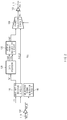
FIG. 2 is a block diagram illustrating a representation of an example of a semiconductor device according to an embodiment of the present disclosure. - The semiconductor device may correspond to any one of the first to
third semiconductor devices FIG. 1 . In the case of using thefirst semiconductor device 10 ofFIG. 1 , a reception-end transmission line L_R may correspond to the first transmission line L1. In the case of using thesecond semiconductor device 20 ofFIG. 1 , a reception-end transmission line L_R may correspond to the second transmission line L2. In the case of using thethird semiconductor device 30 ofFIG. 1 , a reception-end transmission line L_R may correspond to the third transmission line L3. In the case of using thefirst semiconductor device 10 ofFIG. 1 , a transmission-end transmission line L_T may correspond to the second transmission line L2. In the case of using thesecond semiconductor device 20 ofFIG. 1 , a transmission-end transmission line L_T may correspond to the third transmission line L3. In the case of using thethird semiconductor device 30 ofFIG. 1 , a transmission-end transmission line L_T may correspond to the first transmission line L1. - Referring to
FIG. 2 , the semiconductor device may include areceiver 100, adestination decision circuit 110, adata processor 120, an internalpacket generation circuit 130, a selectionsignal generation circuit 140, apacket selection circuit 150, and atransmitter 160. - The
receiver 100 may receive a packet (PKT_R) through the transmission line L_R. - The
destination decision circuit 110 may compare destination information of the packet (PKT_R) with ID information of the semiconductor device 2, and may transmit the packet (PKT_R) to thedata processor 120 or thepacket selection circuit 150 on the basis of the result of comparison. In accordance with one embodiment, when the destination information of the packet (PKT_R) is identical to the ID information of the semiconductor device 2, thedestination decision circuit 110 may transmit the packet (PKT_R) to thedata processor 120. When the destination information of the packet (PKT_R) is not identical to the ID information of the semiconductor device 2, thedestination decision circuit 110 may transmit the packet (PKT_R) to thepacket selection circuit 150. - The
data processor 120 may process the packet (PKT_R) received from thedestination decision circuit 110. - The internal
packet generation circuit 130 may generate an internal packet (IPKT). The internal packet (IPKT) may include data (IDTA) and a header having destination information (IDST). In accordance with one embodiment, the destination information (IDST) contained in the internal packet (IPKT) and the data (IDTA) may be received from thedata processor 120. The destination information (IDST) and the data (IDTA) may be generated on the basis of the processed result of the packet (PKT_R), and may also be generated irrespective of the packet (PKT_R). - The selection
signal generation circuit 140 may activate a selection signal (SEL) upon receiving a packet (PKT_R). The selectionsignal generation circuit 140 may deactivate the selection signal (SEL) when the packet (PKT_R) is not received. - The
packet selection circuit 150 may select any one of the packet (PKT_R) and the internal packet (IPKT), and may transmit the selected packet (PKT_T) to the transmission line (L_T). In accordance with one embodiment, thepacket selection circuit 150 may select the packet (PKT_R) when the selection signal (SEL) is activated. In addition, thepacket selection circuit 150 may select the internal packet (IPKT) when the selection signal (SEL) is deactivated. - The
transmitter 160 may output the selected packet (PKT_T) to the transmission line (L_T). -
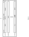
FIG. 3 is a block diagram illustrating a representation of an example of apacket 3 according to an embodiment of the present disclosure. - The
packet 3 inFIG. 3 may correspond to at least one of a first packet (PKT1), a second packet (PKT2), and a third packet (PKT3) illustrated inFIG. 1 , or may correspond to at least one of the packet (PKT_R), the internal packet (IPKT), and the selected packet (PKT_T) illustrated inFIG. 2 . - Referring to
FIG. 3 , thepacket 3 may include a plurality of flits (FLIT1∼FLITn). Each of the respective flits (FLIT1∼FLITn) may be a bitstream having a predetermined length (the number of bits, for example, 128 bits). The first flit (FLIT1) may include a header region, and the last flit (FLITn) may include a tail region. Each of destination information and source information may be included in at least one of the header region and the tail region. - Data (DATA) may be included in the remaining part other than the header region and the tail region of each of the flits FLIT1 to FLITn. Data (DATA) may sequentially include the range from the next part (i.e., 65-th bit (Bit64) of the first flit (FLIT1)) of the header region to a previous part (i.e., 64-th bit (Bit63) of the last flit (FLITn)) of the tail region. That is, the 65-th bit (Bit64) of the first flit (FLIT1) may include a Least Significant Bit (LSB), and the 64-th bit (Bit63) of the last flit (FLITn) may include a Most Significant Bit (MSB).
- Although the
packet 3 ofFIG. 3 includes a plurality of flits FLIT1 to FLITn for convenience of description, thepacket 3 may also include only one flit as necessary. In this case, only one flit includes a header, data (DATA), and a tail. - Although the header of
FIG. 3 is composed of 64 bits and the tail ofFIG. 3 is composed of 64 bits for convenience of description, it should be noted that the number of bits contained in the header and the number of bits contained in the tail are not limited thereto. -
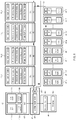
FIGS. 4 to 8 are schematic diagrams illustrating representations of examples of semiconductor systems according to an embodiment of the present disclosure. - In each of
FIGS. 4 to 8 , only one transmission line La, Lb, Lc, Ld, or Le is illustrated for convenience of description and better understanding of the present disclosure. However, the scope or spirit of the present disclosure is not limited thereto, each of the transmission lines (La∼Le) shown inFIGS. 4 to 8 may denote a data transmission direction. Each of the transmission lines (La∼Le) may include a plurality of segments to interconnect a plurality of devices in the form of a loop as shown inFIG. 1 . - Referring to
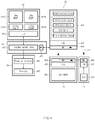
FIG. 4 , a semiconductor system may include aCPU 41, asystem agent 42, asystem memory 43, animage input device 44, aGPU 45, and animage output device 46. InFIG. 4 , thefirst semiconductor device 10 ofFIG. 1 may correspond to thesystem memory 43, thesecond semiconductor device 20 ofFIG. 1 may correspond to theimage input device 44, and thethird semiconductor device 30 ofFIG. 1 may correspond to theGPU 45. - The
CPU 41 may includeCPU bodies L2 caches CPU bodies L2 caches CPU bodies CPU bodies system memory 44, and may store the received command and data. TheLLC 413 may be a cache memory that has lower operation speed and larger capacity as compared to the L1/L2 caches LLC 413 may be coupled to the L1/L2 caches CPU bodies - Although the embodiment has exemplarily disclosed that two
CPU bodies L2 caches - The
system agent 42 may be coupled to theCPU 41, thesystem memory 43, and theimage output device 46, and may control data communication among theCPU 41, thesystem memory 44, and theimage output device 46. Thesystem agent 42 may include asystem agent body 421 and a memory controller (MC) 422. The memory controller (MC) 422 may control data transmission/reception when transmitting/receiving data to/from thesystem memory 43. - The
system memory 43 may correspond to thefirst semiconductor device 10 ofFIG. 1 , may be coupled to the memory controller (MC) 422 of thesystem agent 42, and may be coupled to theimage input device 44 and theGPU 45 in the form of a loop shape. Thesystem memory 43 may include adata storage region 431, acalculation logic circuit 432, and amemory controller 433. Thesystem memory 43 may be implemented as a DRAM. Thedata storage region 431 may store an application code for system calculation, primitive data for image processing in theGPU 45, rendered data, CMOS Image Sensor (CIS) data, and frame buffer data. A calculation logic circuit (CAL) 432 may perform calculation (e.g., data compression) of input data received through the memory controller (MC) 433, and may store the calculation result in thestorage region 431. The memory controller (MC) 433 may receive data from the memory controller (MC) 422 of thesystem agent 42, may transmit the received data to theCAL 432, and may store the resultant data in thedata storage region 431. In addition, the memory controller (MC) 433 may receive packet-shaped data from the memory controller (MC) 453 of theGPU 45, and may transmit the received data to theimage input device 44 according to destination information contained in the packet. The memory controller (MC) 433 may include areceiver 100, adestination decision circuit 110, an internalpacket generation circuit 130, a selectionsignal generation circuit 140, apacket selection circuit 150, and atransmitter 160 as illustrated inFIG. 2 . TheCAL 432 and/or thedata storage region 431 may correspond to thedata processor 120 ofFIG. 2 . - The
image input device 44 may correspond to thesecond semiconductor device 20 ofFIG. 1 , may receive image data from the external part, and may output the received image data in the form of digital data. Theimage input device 44 may include a CIS (CMOS Image Sensor) 441, an Image Signal Processor (ISP) 442, and a memory controller (MC) 443. The memory controller (MC) 443 may receive packet-shaped data from the memory controller (MC) 433 of thesystem memory 43, and may transmit the received packet data to theGPU 45 according to destination information contained in the packet. The memory controller (MC) 443 may include areceiver 100, adestination decision circuit 110, an internalpacket generation circuit 130, a selectionsignal generation circuit 140, apacket selection circuit 150, and atransmitter 160 illustrated inFIG. 2 . TheISP 442 may correspond to thedata processor 120 ofFIG. 2 . - The
GPU 45 may correspond to thethird semiconductor device 30 ofFIG. 1 , and may be a calculation device specialized for image data processing. TheGPU 45 may include aGPU body 451, anLLC 452, and a memory controller (MC) 453. Thememory controller 453 may receive packet-shaped data from thememory controller 443 of theimage input device 44, and may transmit the received packet data to the memory controller (MC) 433 of thesystem memory 43 according to destination information contained in the packet. Thememory controller 453 may include areceiver 100, adestination decision circuit 110, an internalpacket generation circuit 130, a selectionsignal generation circuit 140, apacket selection circuit 150, and atransmitter 160 illustrated inFIG. 2 . TheGPU body 451 and/or theLLC 452 may correspond to thedata processor 120 ofFIG. 2 . - The
image output device 46 may include adisplay controller 461 and adisplay device 462. Thedisplay controller 461 may be coupled to thesystem agent 42, may receive frame buffer data from thesystem memory 43 through thesystem agent 42, and may display the received frame buffer data on thedisplay device 462. - The operations of the
semiconductor system 41 are as follows. - Upon receiving a command from the user, the
system agent 42 may store an application code in thedata storage region 431 of thesystem memory 43. TheCPU bodies LLC 413, and may store a portion of the stored application code parts in the L1/L2 caches CPU body 411a may receive a necessary application code from the L1/L2 cache 412a, and theCPU body 411b may receive a necessary application code from the L1/L2 cache 412b, such that theCPU bodies - When image calculation is needed, the
system agent 42 may store a GPU calculation command in thedata storage region 431 of thesystem memory 43. The GPU calculation command stored in thesystem memory 43 may be transmitted to theGPU 45 after passing through theimage input device 44 along the loop-shaped transmission line La, and may then be stored in theLLC 452. TheGPU body 451 may construct a primitive data storage for storing primitive data, a rendered data storage for storing rendered data, and a frame buffer for storing frame buffer data in thedata storage region 431 of thesystem memory 43 along the loop-shaped transmission line La, and may then perform image calculation using the constructed storages. The completely-processed image data may be stored in the frame buffer. Thesystem agent 42 may read frame buffer data stored in the frame buffer, and may transmit the read frame buffer data to thedisplay controller 461. Thedisplay controller 461 may output frame buffer data to thedisplay device 462. - The
ISP 442 of theimage input device 44 may allow CIS data received from theCIS 441 to pass through theGPU 45 along the loop-shaped transmission line (La), and may store the resultant CIS data in a CIS data storage of thedata storage region 431 of thesystem memory 43. The calculation logic circuit (CAL) 431 of thesystem memory 43 may compress image data received from the imagedata input circuit 45, and may store the compressed image data in thedata storage region 451. TheGPU 45 may receive CIS data stored in the CIS data storage along the loop-shaped transmission line La, and may process the received CIS data. In this case, the image data is compressed and stored, resulting in reduction of the amount of transmission data on the transmission line La. In accordance with one embodiment, theCAL 432 of thesystem memory 43 may perform some parts of image calculation to be performed by theGPU 45. In this case, load of theGPU 45 may be reduced. - In accordance with one embodiment, the
CPU 41, thesystem memory 43, and theimage output device 46 may be coupled to thesystem agent 42. Thesystem memory 43, theimage input device 44, and theGPU 45 may be interconnected through the transmission line La in the form of a loop shape. Accordingly, theimage input device 44 and theGPU 45 may be coupled to thesystem memory 43 without passing through thesystem agent 42, such that load of thesystem agent 42 is reduced, resulting in improvement of overall system performance. -
FIGS. 5 to 8 are schematic diagrams illustrating representations of examples of semiconductor systems according to an embodiment of the present disclosure. The semiconductor systems shown inFIGS. 5 to 8 may be obtained by modification of some structures of the semiconductor system ofFIG. 4 . - Referring to
FIG. 5 , the semiconductor system may include a plurality of image input devices 44_1 to 44_n. Thesystem memory 43, the plurality of image input devices 44_1 to 44_n, and theGPU 45 may be coupled to one another through the transmission line Lb in the form of a loop shape. TheCPU 41, thesystem agent 42, thesystem memory 43, theGPU 45, and theimage output device 46 ofFIG. 5 may be identical to those ofFIG. 4 , and as such a detailed description thereof will herein be omitted for convenience of description and better understanding of the present disclosure. - The respective structures of the image input devices 44_1 to 44_n may correspond to the
image input device 44 ofFIG. 4 . However, image data received from the image input device 44_1 may be stored in thesystem memory 43 after passing through the image input devices 44_2 to 44_n and theGPU 45. Image data received from the image input device 44_2 may be stored in thesystem memory 43 after passing through the image input devices 44_3 to 44_n and theGPU 45 through the transmission line Lb. Image data received from the image input device (44_k, where 1≤k≤n-1) may be stored in thesystem memory 43 after passing through the image input devices 44_k+1 to 44_n and theGPU 45 along the transmission line Lb. Image data received through the image input device 44_n may be stored in thesystem memory 43 after passing through theGPU 45 along the transmission line Lb. - The
GPU 45 may receive image data stored in thesystem memory 43 through the image input devices 44_1 to 44_n so as to perform image data processing. - Referring to
FIG. 6 , the semiconductor system may include a plurality of GPUs 45_1 to 45_n. Thesystem memory 43, theimage input device 44, and the plurality of GPUs 45_1 to 45_n may be coupled to one another through the transmission line Lc in the form of a loop shape. TheCPU 41, thesystem agent 42, thesystem memory 43, theimage input device 44, and theimage output device 46 ofFIG. 6 are identical to those ofFIG. 4 , and as such a detailed description thereof will herein be omitted for convenience of description. - The respective structures of the GPUs 45_1 to 45_n may correspond to the
GPU 45 ofFIG. 4 . However, data stored in thesystem memory 43 may be transmitted to the GPU 45_1 after passing through theimage input device 44 along the transmission line Lc, and data processed by the GPU 45_1 may be stored in thesystem memory 43 after passing through the GPUs 45_2 to 45_n through the transmission line Lc. In addition, data stored in thesystem memory 43 may be transmitted to the GPU 45_2 after passing through theimage input device 44 and the GPU 45_1 along the transmission line Lc, and data processed by the GPU 45_2 may be stored in thesystem memory 43 after passing through the GPUs 45_3 to 45_n along the transmission line Lc. Likewise, data stored in thesystem memory 43 may be transmitted to the GPU 45_k+1 after passing through theimage input device 44 and the GPUs (45_1 to 45_k, where 1≤k≤n-2) along the transmission line Lc, and data processed by the GPU 45_k+1 may be stored in thesystem memory 43 after passing through the GPUs 45_k+2 to 45_n along the transmission line Lc. In addition, data stored in thesystem memory 43 may be transmitted to the GPU 45_n after passing through theimage input device 44 and the GPUs 45_1 to 45_n-1 along the transmission line Lc, and data processed by the GPU 45_n may be stored in thesystem memory 43 through the transmission line Lc. - Referring to
FIG. 7 , the semiconductor system may include a plurality of image input devices 44_1 to 44_m and a plurality of GPUs 45_1 to 45_n. Thesystem memory 43, the plurality of image input devices 44_1 to 44_m, and a plurality of GPUs 45_1 to 45_n may be coupled to one another through the transmission line Ld in the form of a loop shape. TheCPU 41, thesystem agent 42, thesystem memory 43, theGPU 45, and theimage output device 46 ofFIG. 7 are identical to those ofFIG. 4 , and as such a detailed description thereof will herein be omitted for convenience of description. - In
FIG. 7 , CIS data received through any one of the image input devices 44_1 to 44_m may be stored in thesystem memory 43 after passing through at least one left image input device (e.g., the image input device 44_1 may not pass through other image input devices) and the plurality of GPUs 45_1 to 45_n in the arrow direction ofFIG. 7 . Image data processed by any one of the GPUs 45_1 to 45_n may be stored in thesystem memory 43 after passing through at least one left GPU (e.g., the GPU 45_1 may not pass through other GPUs) in the arrow direction ofFIG. 7 . Data stored in thesystem memory 43 may be transmitted to any one of the GPUs 45_1 to 45_n after passing through the plurality of image input devices 44_1 to 44_m and at least one right GPU (e.g., the GPU 45_1 may not pass through other GPUs) in the arrow direction ofFIG. 7 . - Referring to
FIG. 8 , the semiconductor system may include a plurality of system memories 43_1 to 43_I, a plurality of image input devices 44_1 to 44_m, and a plurality of GPUs 45_1 to 45_n. The plurality of system memories 43_1 to 43_I, the plurality of image input devices 44_1 to 44_m, and the plurality of GPUs 45_1 to 45_n may be coupled to one another through the transmission line Le in the form of a loop shape. TheCPU 41, thesystem agent 42, and theimage output device 46 ofFIG. 8 are identical to those ofFIG. 4 , and as such a detailed description thereof will herein be omitted for convenience of description. - A data transmission scheme for use in the loop formed by the plurality of system memories 43_1 to 43_I, the plurality of image input devices 44_1 to 44_m, and the plurality of GPUs 45_1 to 45_n may be similar to those of
FIGS. 4A to 4D . In more detail, in order to store CIS data received from any one of the plurality of image input devices 44_1 to 44_m in any one of the plurality of system memories 43_1 to 43_I, the CIS data must pass through a plurality of devices disposed between a corresponding image input device and a corresponding system memory in the arrow direction. In order to transmit data from any one of the GPUs 45_1∼45_n to any one of the system memories 43_1∼43_I, the data may pass through a plurality of devices disposed between a corresponding GPU and a corresponding system memory in the arrow direction. -
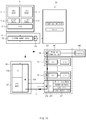
FIGS. 9 to 11 are schematic diagrams illustrating representation of examples of semiconductor systems according to an embodiment of the present disclosure. Only one transmission line Lf is exemplarily shown inFIG. 9 , only one transmission line Lg is exemplarily shown inFIG. 10 , and only one transmission line Lh is exemplarily shown inFIG. 11 . Each transmission line Lf, Lg, or Lh may indicate a data transmission direction. Each transmission line Lf, Lg, or Lh may be composed of a plurality of segments so as to interconnect a plurality of devices in the form of a loop shape as shown inFIG. 1 . - Referring to
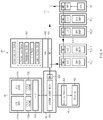
FIG. 9 , the semiconductor system may include aCPU 51, asystem agent 52, asystem memory 53, animage input device 54, aGPU 55, animage output device 56, and agraphics memory 57. InFIG. 9 , thefirst semiconductor device 10 ofFIG. 1 may correspond to thegraphics memory 57, thesecond semiconductor device 20 ofFIG. 1 may correspond to theimage output device 56, and thethird semiconductor device 30 ofFIG. 1 may correspond to theimage input device 54. InFIG. 9 , the same constituent elements as inFIG. 4 will herein be omitted for convenience of description. - The
CPU 51 may correspond to theCPU 41 ofFIG. 4 , and as such a detailed description thereof will herein be omitted for convenience of description. - The
system agent 52 may correspond to thesystem agent 42 ofFIG. 4 , may be coupled to theCPU 51, thesystem memory 53, and theGPU 55, such that thesystem agent 52 may control data communication among theCPU 51, thesystem memory 53, and theGPU 55. - The
system memory 53 may be coupled to the memory controller 532 of thesystem agent 52. Thesystem memory 53 may store an application code and data needed for system calculation. - The
graphics memory 57 may correspond to thefirst semiconductor device 10 ofFIG. 1 , and may store data associated with the image calculation operation of theGPU 55. Thegraphics memory 57 may be implemented as a High Bandwidth Memory (HBM). Thegraphics memory 57 may be coupled to theimage output device 56 and theimage input device 54 through the transmission line (Lf) in the form of a loop shape. Thegraphics memory 57 may include adata storage region 571, a calculation logic circuit (CAL) 572, and amemory controller 573. Thedata storage region 571 may store primitive data for image processing in theGPU 55, rendered data, CIS data, and frame buffer data. TheCAL 572 may perform calculation operation (e.g., compression operation) for data received through the memory controller (MC) 573, and may store the calculated (or compressed) data in thedata storage region 571. In accordance with one embodiment, theCAL 572 may also perform some parts of the image calculation operation of theGPU 55. The memory controller (MC) 573 may communicate with the memory controller (MC) 553 of theGPU 55. In addition, the memory controller (MC) 573 may receive packet-shaped data from the memory controller (MC) 543 of theimage input device 54, and may transmit the received data to theimage output device 56 according to destination information contained in the packet. Thememory controller 573 may include areceiver 100, adestination decision circuit 110, an internalpacket generation circuit 130, a selectionsignal generation circuit 140, apacket selection circuit 150, and atransmitter 160. TheCAL 572 and/or thedata storage region 571 may correspond to thedata processor 120 ofFIG. 2 . - The
image output device 56 may correspond to thesecond semiconductor device 20 ofFIG. 1 , and may be coupled to theimage input device 54 and thegraphics memory 57 through the transmission line Lf in the form of a loop shape. Theimage output device 56 may include adisplay controller 561, adisplay device 562, and amemory controller 563. The memory controller (MC) 563 may receive packet-shaped data from the memory controller (MC) 573 of thegraphics memory 57, and may transmit the received data to theimage input device 54 according to destination information contained in the packet. The memory controller (MC) 563 may include areceiver 100, adestination decision circuit 110, an internalpacket generation circuit 130, a selectionsignal generation circuit 140, apacket selection circuit 150, and atransmitter 150 ofFIG. 2 . Thedisplay controller 561 may correspond to thedata processor 120 ofFIG. 2 . - The
image input device 54 may correspond to thethird semiconductor device 30 ofFIG. 1 , and may be coupled to thegraphics memory 57 and theimage output device 56 through the transmission line (Lf) in the form of a loop shape. Theimage input device 54 may include aCIS 541, anISP 542, and a memory controller (MC) 543. The memory controller (MC) 543 may receive packet-shaped data from the memory controller (MC) 563 of theimage output device 56, and may transmit the received data to thegraphics memory 57 according to destination information contained in the packet. The memory controller (MC) 543 may include areceiver 100, adestination decision circuit 110, an internalpacket generation circuit 130, a selectionsignal generation circuit 140, apacket selection circuit 150, and atransmitter 160 ofFIG. 2 . TheISP 542 may correspond to thedata processor 120 ofFIG. 2 . - The
GPU 55 may include aGPU body 551, anLLC 552, and a memory controller (MC) 553. TheGPU body 551 may perform calculation related to image processing. TheLLC 552 may store some parts of the application code needed to operate theGPU body 551. Thememory controller 553 may control data communication between theGPU body 551 and thegraphics memory 57. - The operations of the semiconductor system will hereinafter be described in detail.
- Upon receiving a command from the user, the
system agent 52 may store an application code in thesystem memory 53. TheCPU bodies LLC 513, and may store some parts of the stored application code parts in the L1/L2 caches CPU body 511a may read a necessary application code from the L1/L2 cache 512a, and theCPU body 511b may read a necessary application code from the L1/L2 cache 512b, such that theCPU bodies - When image calculation is needed, the
system agent 52 may store a GPU calculation command stored in thesystem memory 53 in theLLC 552 of theGPU 55. TheGPU body 551 may construct a primitive data storage for storing primitive data, a rendered data storage for storing rendered data, and a frame buffer for storing frame buffer data in thedata storage region 571 of thesystem memory 57, and may then perform image calculation using the constructed storages. The completely-processed image data may be stored in the frame buffer. The frame buffer data stored in the frame buffer may be constructed in the form of a packet, and may then be transmitted to theimage output device 56 along the transmission line Lf. Thememory controller 563 of theimage output device 56 may transmit the packet to thedisplay controller 561, and thedisplay controller 561 may output frame buffer data contained in the packet to thedisplay device 562. - The
ISP 542 of theimage input device 54 may store CIS data received from theCIS 541 in the CIS data storage of thedata storage region 571 of thegraphics memory 57 along the transmission line Lf. TheCAL 572 of thegraphics memory 57 may compress CIS data received from the imagedata input circuit 54, and may store the compressed CIS data in thedata storage region 571. TheGPU 55 may receive image data stored in the CIS data storage, and may process the received image data. In this case, since image data is compressed and stored, the amount of data transmission on the transmission line Lf may be reduced. - The semiconductor systems will hereinafter be described with reference to
FIGS. 10 and11 . The semiconductor systems may be obtained by modification of some structures of the semiconductor system ofFIG. 9 . -
FIG. 10 is a schematic diagram illustrating a representation of an example of the semiconductor system according to an embodiment of the present disclosure. - Referring to
FIG. 10 , the semiconductor system may include aCPU 51, asystem agent 52, asystem memory 53, a plurality of image input devices 54_1 to 54_p, aGPU 55, animage output device 56, and agraphics memory 57. TheGPU 55, theimage output device 56, the plurality of image input devices 54_1 to 54_p, and thegraphics memory 57 may be coupled to one another through the transmission line Lg in the form of a loop shape. - The
memory controller 553 of theGPU 55 may receive packet-shaped data from the memory controller (MC) 573 of thegraphics memory 57, and may transmit the received data to theimage output device 56 according to destination information contained in the packet. Thememory controller 553 may include areceiver 100, adestination decision circuit 110, an internalpacket generation circuit 130, a selectionsignal generation circuit 140, apacket selection circuit 150, and atransmitter 160 illustrated inFIG. 2 . TheGPU body 551 may correspond to thedata processor 120 ofFIG. 2 . - Image data generated from any one of the plurality of image input devices 54_1 to 54_p may be stored in the
graphics memory 57 after passing through at least one of other image input devices located in a lower part ofFIG. 10 . However, image data generated from the image input device 54_p located at the lowest part ofFIG. 10 may be stored in thegraphics memory 57 without passing through other image input devices. - Image data stored in the
graphics memory 57 may be transmitted to theGPU 55 through the transmission line Lg. In accordance with one embodiment, a transmission line for coupling thegraphics memory 57 to theGPU 55 may be used, separately from the transmission line Lg. In this case, a bandwidth between thegraphics memory 57 and theGPU 55 may be increased so that a data transfer rate may be increased. The image data processed by theGPU 55 may be transmitted or output to theimage output device 56 along the arrow direction, and may be stored in thegraphics memory 57 after passing through theimage output device 56 and the plurality of image input devices 54_1 to 54_p. -
FIG. 11 is a schematic diagram illustrating a representation of an example of the semiconductor system according to an embodiment of the present disclosure. - Referring to
FIG. 11 , the semiconductor system may include asystem agent 52, asystem memory 53, a plurality of image input devices 54_1 to 54_p, aGPU 55, a plurality of image output devices 56_1 to 56_q and agraphics memory 57. TheGPU 55, the plurality of image output devices 56_1 to 56_q, the plurality of image input devices 54_1 to 54_p, and thegraphics memory 57 may be coupled to one another through the transmission line Lh in the form of a loop shape. - Any one of the plurality of image output devices 56_1 to 56_q may receive frame buffer data stored in the
graphics memory 57, after passing through theGPU 55 and at least one of other image output devices located at an upper part ofFIG. 11 in the arrow direction. However, the image output device 56_1 located at the highest part ofFIG. 11 may receive frame buffer data after passing through only theGPU 55. -
FIG. 12 is a schematic diagram illustrating a semiconductor system according to an embodiment of the present disclosure.FIG. 12 illustrates a System In Package (SIP) in which a dotted part of the semiconductor system ofFIG. 9 and theGPU 55 are implemented as a single package. - Referring to
FIG. 12 , the semiconductor system 6 may include asubstrate 610, aGPU 65, agraphics memory 67, animage output device 66, and animage input device 64. TheGPU 65, thegraphics memory 67, theimage output device 66, and theimage input device 64 may respectively correspond to theGPU 55, thegraphics memory 57, theimage output device 56, and theimage input device 54 ofFIG. 9 . - The
graphics memory 67 may include a stacked structure of a plurality of dies D0 to D4. The first die D0 may include a memory controller MC, a calculation logic circuit CAL, and a physical layer PHY. The memory controller MC and the CAL of the first die D0 may respectively correspond to thememory controller MC 573 and theCAL 572 ofFIG. 9 . The physical layer PHY may control data transmission along with the physical layer PHY of theGPU 65. The second to third dies D1 to D4 may correspond to thedata storage region 571 of thegraphics memory 57 shown inFIG. 9 . The second to fifth dies D1, D2, D3, and D4 may respectively include a first core (Core1), a second core (Core2), a third core (Core3), and a fourth core (Core4). A first channel CH1, a second channel CH2, a third channel CH3, and a fourth channel CH4 may be respectively allocated to the first core (Core1), the second core (Core2), the third core (Core3), and the fourth core (Core4), and the respective channels (CH1∼CH4) may be read or written independently from each other. - Each of the
GPU 55, thegraphics memory 57, theimage output device 56, and theimage input device 55 may be coupled to thesubstrate 610 through an interposer. Thegraphics memory 57, theimage output device 56, and theimage input device 55 may be coupled to one another through the transmission line Lf in the form of a loop shape. Although not shown inFIG. 12 , theimage output device 56 and thegraphics memory 57 may be coupled to each other through the transmission line Lf. TheGPU 55 and thegraphics memory 57 may communicate with each other at high speed through each physical layer PHY. - Although the
GPU 55 and the dotted part ofFIG. 9 are implemented as a System In Package (SIP) for convenience of description and better understanding of the present disclosure, the scope or spirit of the present disclosure is not limited thereto. TheGPU 55 and the dotted part ofFIG. 10 may be implemented as a System In Package (SIP), or theGPU 55 and the dotted part ofFIG. 11 may be implemented as a System In Package (SIP). In addition, theGPU 55 and thegraphics memory 57 ofFIG. 9 may be implemented as a first SIP, and theimage output device 56 and theimage input device 54 may be implemented as a second SIP, such that the first SIP and the second SIP may be respectively attached to a front surface and a rear surface of the substrate (e.g., PCB) as necessary. -
FIG. 13 is a conceptual diagram illustrating a representation of an example of a semiconductor system according to an embodiment of the present disclosure. - Referring to
FIG. 13 , the semiconductor system may include a loop-shaped transmission line L, and fourth tosixth semiconductor devices FIG. 13 exemplarily discloses threesemiconductor devices FIG. 13 may also include at least two semiconductor devices without departing from the scope or spirit of the present disclosure. - Each of the
respective semiconductor devices semiconductor devices -
FIG. 14 is a block diagram illustrating a representation of an example of a semiconductor device according to an embodiment of the present disclosure. - The semiconductor device may correspond to at least one of the fourth to
sixth semiconductor devices FIG. 13 . - Referring to
FIG. 14 , the semiconductor device may include areceiver 800, adestination decision circuit 810, adata processor 820, an internalpacket generation circuit 830, atransmission circuit 840, and atransmitter 850. InFIG. 14 , the transmission line L may correspond to the loop-shaped transmission line (L) ofFIG. 13 . - The
receiver 800 may detect the packet (PKT) on the transmission line L, and may transmit the detected packet (PKT) to thedestination decision circuit 810. - The
destination decision circuit 810 may transmit the packet (PKT) to thedata processor 820 on the basis of destination information of the packet (PKT). The packet (PKT) may have the structure of thepacket 3 shown inFIG. 3 . Thedestination decision circuit 810 may compare destination information of the packet (PKT) with ID information of the semiconductor device. When the destination information of the packet (PKT) is identical to ID information of the semiconductor device, thedestination decision circuit 810 may transmit the packet (PKT) to thedata processor 820. When the destination information of the packet (PKT) is not identical to ID information of the semiconductor device, thedestination decision circuit 810 may not transmit the packet (PKT) to thedata processor 820. - The
data processor 820 may process the packet (PKT). Thedata processor 820 may generate internal destination information (IDST) and internal data (IDTA). The internal destination information (IDST) and the internal data (IDTA) may be generated on the basis of the processing result of the packet (PKT), and may also be generated irrespective of the packet (PKT). - The internal
packet generation circuit 830 may generate the internal packet (IPKT) using the internal destination information (IDST) and the internal data (IDTA). The internal packet (IPKT) may have the structure of thepacket 3 shown inFIG. 3 . The internal packet (IPKT) may correspond to one of the packets (PKT4∼PKT6) ofFIG. 13 . - The
transmission circuit 840 may transmit the internal packet (IPKT) to the transmission line L. Thetransmission circuit 840 may detect the presence or absence of a standby state of the transmission line L, and may transmit the internal packet (IPKT) to the transmission line L according to the result of detection. For example, when a voltage of the transmission line L is equal to or higher than a predetermined level, this means that the transmission line L is currently used and enters a standby mode. When the voltage of the transmission line L is less than the predetermined level, this means that the transmission line L is in the standby mode such that the transmission line L may transmit the internal packet (IPKT). Thetransmission circuit 840 may detect the voltage of the transmission line L at intervals of a predetermined time. - The
transmitter 850 may transmit the internal packet (IPKT) received from thetransmission circuit 840 to the transmission line L. -
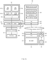
FIG. 15 is a block diagram illustrating a representation of an example of a semiconductor system according to an embodiment of the present disclosure. - The semiconductor system of
FIG. 15 may correspond to the semiconductor system ofFIG. 4 . Whereas thesystem memory 43, theimage input device 44, and theGPU 45 ofFIG. 4 are coupled to one another through the transmission line La in the form of a loop shape, the semiconductor system may enables asystem memory 93, animage input device 94, and aGPU 95 to be coupled to the loop-shaped transmission line Li. - The
system memory 93, theimage input device 94, and theGPU 95 may respectively correspond to thefourth semiconductor device 40, thefifth semiconductor device 50, and thesixth semiconductor device 60 ofFIG. 13 . Each of anMC 933 of thesystem memory 93, anMC 943 of theimage input device 94, and anMC 953 of theGPU 95 may include areceiver 800, adestination decision circuit 810, an internalpacket generation circuit 830, atransmission circuit 840, and atransmitter 850 ofFIG. 14 . ACAL 932 and/or adata storage region 931 of thesystem memory 93, anISP 942 of theimage input device 94, aGPU body 951 and/or anLLC 952 of theGPU 95 may correspond to thedata processor 820 ofFIG. 14 . - The basic operations of the above-mentioned constituent elements are identical to those of the semiconductor system of
FIG. 4 . However, data communication between thesystem memory 93, theimage input device 94, and theGPU 95 may be achieved through the loop-shaped transmission line (Li) as shown inFIGS. 13 and14 . -
FIG. 16 is a block diagram illustrating a representation of an example of a semiconductor system according to an embodiment of the present disclosure. The semiconductor system ofFIG. 16 may correspond to the semiconductor system ofFIG. 9 . Whereas thegraphics memory 57, theimage output device 56, and theimage input device 54 ofFIG. 9 are coupled to one another through the transmission line Lf in the form of a loop shape, the semiconductor system may enables agraphics memory 1070, animage output device 1060, and animage input device 1040 to be coupled to the loop-shaped transmission line Lj. - The
graphics memory 1070, theimage output device 1060, and theimage input device 1040 may respectively correspond to thefourth semiconductor device 40, thefifth semiconductor device 50, and thesixth semiconductor device 60 ofFIG. 13 . Each of anMC 1073 of thegraphics memory 1070, anMC 1063 of theimage output device 1060, and anMC 1043 of theimage input device 1040 may include areceiver 800, adestination decision circuit 810, an internalpacket generation circuit 830, atransmission circuit 840, and atransmitter 850 ofFIG. 14 . ACAL 1072 and/or adata storage region 1071 of thegraphics memory 1070, adisplay controller 1061 of theimage output device 1060, and anISP 1042 of theimage input device 1040 may correspond to thedata processor 820 ofFIG. 14 . - The basic operations of the above-mentioned constituent elements are identical to those of the semiconductor system of
FIG. 9 . However, data communication between thegraphics memory 1070, theimage output device 1060, and theimage input device 1040 may be achieved through the loop-shaped transmission line (Lj) as shown inFIGS. 13 and14 . - Although
FIGS. 15 and16 have been exemplarily disclosed as examples of the semiconductor system, the scope or spirit of the present disclosure is not limited thereto. For example, as shown inFIGS. 5 to 6 , the semiconductor system according to the embodiment of the present disclosure may include multiple system memories or multiple image input devices or multiple GPUs. At least one system memory, at least one image input device, and at least one GPU may be coupled to the loop-shaped transmission line. - Referring to
FIGS. 10 and11 , the semiconductor system according to an embodiment may include a graphics memory, a GPU, at least one image output device, and at least one image input device. The graphics memory, the GPU, the at least one image output device, and the at least one image input device may be coupled to the loop-shaped transmission line. - When the same kinds of devices (for example, the plurality of image input devices, the plurality of GPUs, the plurality of system memories, and the plurality of image output devices) are used as shown in
FIGS. 5 to 8 ,10 , and11 ,FIGS. 5 to 8 ,10 , and11 have exemplarily disclosed that the same kinds of devices are coupled contiguous to one another. However, the scope or spirit of the present disclosure is not limited thereto, and the same kinds of devices may be located contiguous to one another or may also be arranged with a different type of device interposed therebetween. - Those skilled in the art will appreciate that the invention may be carried out in other specific ways than those set forth herein without departing from the spirit and essential characteristics of the invention. The above embodiments are therefore to be construed in all aspects as illustrative and not restrictive. The scope of the invention should be determined by the appended claims and their legal equivalents, not by the above description. Further, all changes coming within the meaning and equivalency range of the appended claims are intended to be embraced therein. In addition, it is obvious to those skilled in the art that claims that are not explicitly cited in each other in the appended claims may be presented in combination as an embodiment of the invention or included as a new claim by a subsequent amendment after the application is filed.
- The embodiments of the present disclosure may easily increase the number of semiconductor devices contained in the semiconductor system, resulting in increase extensibility.
Claims (20)
- A semiconductor system comprising:a first semiconductor device coupled to a first transmission line, and configured to transmit a first packet to a second transmission line on the basis of first destination information of the first packet received through the first transmission line;a second semiconductor device coupled to the first semiconductor device through the second transmission line, and configured to transmit a second packet to a third transmission line on the basis of second destination information of the second packet received through the second transmission line; anda third semiconductor device coupled to the second semiconductor device through the third transmission line, coupled to the first semiconductor device through the first transmission line, and configured to transmit a third packet to the first transmission line on the basis of third destination information of the third packet received through the third transmission line.
- The semiconductor system according to claim 1, wherein the first semiconductor device includes:
a first destination decision circuit configured to transmit the first packet to the second transmission line on the basis of the result of comparison between the first destination information and identification (ID) information of the first semiconductor device. - The semiconductor system according to claim 2, wherein the first semiconductor device further includes:a first data processor,wherein, when the first destination information is identical to ID information of the first semiconductor device, the first destination decision circuit transmits the first packet to the first data processor.
- The semiconductor system according to claim 1, wherein the first semiconductor device includes:a first internal packet generation circuit configured to generate an internal packet having internal destination information and internal data; anda first packet selection circuit configured to select any one of the first packet and the internal packet, and transmit the selected packet to the second transmission line.
- The semiconductor system according to claim 4, wherein the first semiconductor device further includes:
a first selection signal generation circuit configured to activate a selection signal upon receiving the first packet. - The semiconductor system according to claim 5, wherein the first packet selection circuit selects the first packet when the selection signal is activated.
- The semiconductor system according to claim 1, further comprising:a central processing unit (CPU); anda system agent,wherein the first semiconductor device is a system memory for transmitting/receiving data to/from the central processing unit (CPU) through the system agent,the second semiconductor device is an image input device, andthe third semiconductor device is a graphics processing unit (GPU).
- The semiconductor system according to claim 1, further comprising:a central processing unit (CPU);a system agent; anda system memory configured to transmit/receive data to/from the central processing unit (CPU) through the system agent,wherein the first semiconductor device is a graphics memory,the second semiconductor device is an image output device, andthe third semiconductor device is an image input device.
- The semiconductor system according to claim 1, further comprising:a central processing unit (CPU);a system agent; anda system memory configured to transmit/receive data to/from the central processing unit (CPU) through the system agent,wherein the first semiconductor device is a graphics processing unit (GPU) for transmitting/receiving data to/from the central processing unit (CPU) through the system agent,the second semiconductor device is an image input/output(I/O) device, andthe third semiconductor device is a graphics memory.
- The semiconductor system according to claim 1, further comprising:a graphics processing unit (GPU),wherein the first semiconductor device is a graphics memory,the second semiconductor device is an image output device,the third semiconductor device is an image input device, andthe graphics processing unit (GPU), the first semiconductor device, the second semiconductor device, and the third semiconductor device are grouped into one package.
- A semiconductor device comprising:a receiver configured to receive a packet;a packet generation circuit configured to generate an internal packet having internal destination information and internal data;a packet selection circuit configured to transmit any one of the received packet and the internal packet; anda destination decision circuit configured to transmit the received packet to the packet selection circuit on the basis of destination information of the received packet.
- The semiconductor device according to claim 11, wherein the destination decision circuit transmits the received packet to the packet selection circuit on the basis of the result of comparison between the destination information of the received packet and identification (ID) information of the semiconductor device.
- The semiconductor device according to claim 12, further comprising:a data processor,wherein, when the destination information of the received packet is identical to the ID information of the semiconductor device, the destination decision circuit transmits the received packet to the data processor.
- The semiconductor device according to claim 11, further comprising:
a selection signal generation circuit configured to activate a selection signal upon receiving the packet. - The semiconductor device according to claim 14, wherein the packet selection circuit selects the packet when the selection signal is activated.
- A semiconductor system including a plurality of semiconductor devices coupled to a loop-shaped transmission line, the semiconductor system comprising:
each of the plurality of semiconductor devices including:a data processor;a destination decision circuit configured to transmit the received packet to the data processor on the basis of destination information of the received packet;an internal packet generation circuit configured to generate an internal packet using internal data; anda transmission circuit configured to transmit the internal packet to the loop-shaped transmission line. - The semiconductor system according to claim 16, wherein the internal packet includes destination information and the internal data.
- The semiconductor system according to claim 16, wherein the transmission circuit detects whether the loop-shaped transmission line is in a standby state, and transmits the internal packet to the loop-shaped transmission line.
- The semiconductor system according to claim 16, further comprising:a central processing unit (CPU); anda system agent,wherein the plurality of semiconductor devices include a system memory for transmitting/receiving data to/from the central processing unit (CPU) through the system agent, an image input device, and a graphics processing unit (GPU).
- The semiconductor system according to claim 16, further comprising:a central processing unit (CPU);a system agent; anda system memory configured to transmit/receive data to/from the central processing unit (CPU) through the system agent,wherein the plurality of semiconductor devices include a graphics processing unit (GPU) for transmitting/receiving data to/from the central processing unit (CPU) through the system agent, an image input/output (I/O) device, and a graphics memory.
Applications Claiming Priority (2)
| Application Number | Priority Date | Filing Date | Title |
|---|---|---|---|
| KR1020170146481A KR102433101B1 (en) | 2017-11-06 | 2017-11-06 | Semiconductor device and semiconductor system including thereof |
| PCT/KR2018/006692 WO2019088390A1 (en) | 2017-11-06 | 2018-06-14 | Semiconductor device and semiconductor system including same |
Publications (3)
| Publication Number | Publication Date |
|---|---|
| EP3709179A1 true EP3709179A1 (en) | 2020-09-16 |
| EP3709179A4 EP3709179A4 (en) | 2021-07-28 |
| EP3709179B1 EP3709179B1 (en) | 2023-05-31 |
Family
ID=66332046
Family Applications (1)
| Application Number | Title | Priority Date | Filing Date |
|---|---|---|---|
| EP18873832.2A Active EP3709179B1 (en) | 2017-11-06 | 2018-06-14 | Semiconductor device and semiconductor system including same |
Country Status (4)
| Country | Link |
|---|---|
| US (1) | US11455703B2 (en) |
| EP (1) | EP3709179B1 (en) |
| KR (1) | KR102433101B1 (en) |
| WO (1) | WO2019088390A1 (en) |
Family Cites Families (16)
| Publication number | Priority date | Publication date | Assignee | Title |
|---|---|---|---|---|
| US6891828B2 (en) | 2001-03-12 | 2005-05-10 | Network Excellence For Enterprises Corp. | Dual-loop bus-based network switch using distance-value or bit-mask |
| WO2003083680A1 (en) | 2002-03-22 | 2003-10-09 | Deering Michael F | Scalable high performance 3d graphics |
| US7254665B2 (en) * | 2004-06-16 | 2007-08-07 | Microsoft Corporation | Method and system for reducing latency in transferring captured image data by utilizing burst transfer after threshold is reached |
| WO2007093218A1 (en) | 2006-02-17 | 2007-08-23 | Mentor Graphics Corp. | Ring bus in an emulation environment |
| US20070280141A1 (en) * | 2006-05-01 | 2007-12-06 | Seagate Technology, Llc | Hardware implementation of loop initialization protocol |
| DE102006051136A1 (en) * | 2006-10-30 | 2008-05-08 | Qimonda Ag | Adapter card for use with memory module system i.e. fully buffered-dual in-line memory module system, has memory plug contact for connecting adapter card to memory module e.g. unregistered dual in-line memory module |
| US7801141B2 (en) | 2008-07-25 | 2010-09-21 | Micrel, Inc. | True ring networks with gateway connections using MAC source address filtering |
| JP5539101B2 (en) | 2010-08-18 | 2014-07-02 | キヤノン株式会社 | Information processing apparatus, information processing method, and program |
| KR101150928B1 (en) | 2010-08-26 | 2012-05-29 | 한국과학기술원 | Network architecture and method for processing packet data using the same |
| JP5932242B2 (en) * | 2011-05-20 | 2016-06-08 | キヤノン株式会社 | Information processing apparatus, communication method, and program |
| WO2015074239A1 (en) | 2013-11-22 | 2015-05-28 | Intel Corporation | Method and apparatus to improve performance of chained tasks on a graphics processing unit |
| KR101543671B1 (en) | 2014-04-25 | 2015-08-12 | 송암시스콤 주식회사 | Packet processing method and apparatus in ring network |
| KR102466160B1 (en) | 2016-01-08 | 2022-11-14 | 삼성전자주식회사 | System on chip and integrated chip performing data loopback operation, and mobile device having the same |
| US10061523B2 (en) * | 2016-01-15 | 2018-08-28 | Samsung Electronics Co., Ltd. | Versioning storage devices and methods |
| US10042806B2 (en) | 2016-02-02 | 2018-08-07 | Xilinx, Inc. | System-level interconnect ring for a programmable integrated circuit |
| US20170358132A1 (en) * | 2016-06-12 | 2017-12-14 | Apple Inc. | System And Method For Tessellation In An Improved Graphics Pipeline |
-
2017
- 2017-11-06 KR KR1020170146481A patent/KR102433101B1/en active Active
-
2018
- 2018-06-14 EP EP18873832.2A patent/EP3709179B1/en active Active
- 2018-06-14 WO PCT/KR2018/006692 patent/WO2019088390A1/en not_active Ceased
- 2018-06-14 US US16/769,877 patent/US11455703B2/en active Active
Also Published As
| Publication number | Publication date |
|---|---|
| US11455703B2 (en) | 2022-09-27 |
| US20210183006A1 (en) | 2021-06-17 |
| EP3709179B1 (en) | 2023-05-31 |
| KR102433101B1 (en) | 2022-08-18 |
| EP3709179A4 (en) | 2021-07-28 |
| KR20190051148A (en) | 2019-05-15 |
| WO2019088390A1 (en) | 2019-05-09 |
Similar Documents
| Publication | Publication Date | Title |
|---|---|---|
| US7215561B2 (en) | Semiconductor memory system having multiple system data buses | |
| US20240004419A1 (en) | Computer Architecture Having Selectable Parallel and Serial Communication Channels Between Processors and Memory | |
| US8826101B2 (en) | Memory system and method using a memory device die stacked with a logic die using data encoding, and system using the memory system | |
| US7979629B2 (en) | Memory module and control method of serial peripheral interface using address cache | |
| US6381293B1 (en) | Apparatus and method for serial data communication between plurality of chips in a chip set | |
| US20070150687A1 (en) | Memory system with both single and consolidated commands | |
| US10805392B2 (en) | Distributed gather/scatter operations across a network of memory nodes | |
| US20240403236A1 (en) | Devices using chiplet based storage architectures | |
| US11902706B2 (en) | Method for transmitting high bandwidth camera data through SerDes links | |
| CN111884952B (en) | Multichannel calculation accelerating equipment based on FPGA | |
| EP3709179B1 (en) | Semiconductor device and semiconductor system including same | |
| CN101950279A (en) | Method and bus system for balancing data information flow and decoder | |
| US8854088B2 (en) | Multi-chip system and semiconductor package | |
| CN101004674B (en) | Data processing system and high-definition TV including the data processing system | |
| CN111857817B (en) | Data reading method, data reading device and data reading system | |
| US11636061B2 (en) | On-demand packetization for a chip-to-chip interface | |
| CN112446474B (en) | Chip, multichip system, electronic equipment and data transmission method | |
| US10366646B2 (en) | Devices including first and second buffers, and methods of operating devices including first and second buffers | |
| CN108024033B (en) | Video image sending circuit based on ARINC818 protocol | |
| US7523250B2 (en) | Semiconductor memory system and semiconductor memory chip | |
| TWI760970B (en) | Wireless communication apparatus having memory sharing mechanism and memory sharing method of the same | |
| CN114726925B (en) | Wireless communication device with memory sharing mechanism and memory sharing method thereof | |
| CN214278936U (en) | MCBSP and USB conversion control board card | |
| US20260072866A1 (en) | Bandwidth maximization | |
| KR100248151B1 (en) | Universal receiver transmitter |
Legal Events
| Date | Code | Title | Description |
|---|---|---|---|
| STAA | Information on the status of an ep patent application or granted ep patent |
Free format text: STATUS: THE INTERNATIONAL PUBLICATION HAS BEEN MADE |
|
| PUAI | Public reference made under article 153(3) epc to a published international application that has entered the european phase |
Free format text: ORIGINAL CODE: 0009012 |
|
| STAA | Information on the status of an ep patent application or granted ep patent |
Free format text: STATUS: REQUEST FOR EXAMINATION WAS MADE |
|
| 17P | Request for examination filed |
Effective date: 20200527 |
|
| AK | Designated contracting states |
Kind code of ref document: A1 Designated state(s): AL AT BE BG CH CY CZ DE DK EE ES FI FR GB GR HR HU IE IS IT LI LT LU LV MC MK MT NL NO PL PT RO RS SE SI SK SM TR |
|
| AX | Request for extension of the european patent |
Extension state: BA ME |
|
| DAV | Request for validation of the european patent (deleted) | ||
| DAX | Request for extension of the european patent (deleted) | ||
| REG | Reference to a national code |
Ref country code: DE Ref legal event code: R079 Ref document number: 602018050572 Country of ref document: DE Free format text: PREVIOUS MAIN CLASS: G06F0013380000 Ipc: G06T0001200000 |
|
| A4 | Supplementary search report drawn up and despatched |
Effective date: 20210630 |
|
| RIC1 | Information provided on ipc code assigned before grant |
Ipc: G06T 1/20 20060101AFI20210624BHEP Ipc: G06T 15/00 20110101ALI20210624BHEP Ipc: G06F 13/42 20060101ALI20210624BHEP |
|
| GRAP | Despatch of communication of intention to grant a patent |
Free format text: ORIGINAL CODE: EPIDOSNIGR1 |
|
| STAA | Information on the status of an ep patent application or granted ep patent |
Free format text: STATUS: GRANT OF PATENT IS INTENDED |
|
| INTG | Intention to grant announced |
Effective date: 20221213 |
|
| GRAS | Grant fee paid |
Free format text: ORIGINAL CODE: EPIDOSNIGR3 |
|
| GRAA | (expected) grant |
Free format text: ORIGINAL CODE: 0009210 |
|
| STAA | Information on the status of an ep patent application or granted ep patent |
Free format text: STATUS: THE PATENT HAS BEEN GRANTED |
|
| AK | Designated contracting states |
Kind code of ref document: B1 Designated state(s): AL AT BE BG CH CY CZ DE DK EE ES FI FR GB GR HR HU IE IS IT LI LT LU LV MC MK MT NL NO PL PT RO RS SE SI SK SM TR |
|
| REG | Reference to a national code |
Ref country code: GB Ref legal event code: FG4D Ref country code: CH Ref legal event code: EP |
|
| REG | Reference to a national code |
Ref country code: AT Ref legal event code: REF Ref document number: 1571394 Country of ref document: AT Kind code of ref document: T Effective date: 20230615 Ref country code: DE Ref legal event code: R096 Ref document number: 602018050572 Country of ref document: DE |
|
| REG | Reference to a national code |
Ref country code: IE Ref legal event code: FG4D |
|
| REG | Reference to a national code |
Ref country code: LT Ref legal event code: MG9D |
|
| REG | Reference to a national code |
Ref country code: NL Ref legal event code: MP Effective date: 20230531 |
|
| REG | Reference to a national code |
Ref country code: AT Ref legal event code: MK05 Ref document number: 1571394 Country of ref document: AT Kind code of ref document: T Effective date: 20230531 |
|
| PG25 | Lapsed in a contracting state [announced via postgrant information from national office to epo] |
Ref country code: SE Free format text: LAPSE BECAUSE OF FAILURE TO SUBMIT A TRANSLATION OF THE DESCRIPTION OR TO PAY THE FEE WITHIN THE PRESCRIBED TIME-LIMIT Effective date: 20230531 Ref country code: NO Free format text: LAPSE BECAUSE OF FAILURE TO SUBMIT A TRANSLATION OF THE DESCRIPTION OR TO PAY THE FEE WITHIN THE PRESCRIBED TIME-LIMIT Effective date: 20230831 Ref country code: ES Free format text: LAPSE BECAUSE OF FAILURE TO SUBMIT A TRANSLATION OF THE DESCRIPTION OR TO PAY THE FEE WITHIN THE PRESCRIBED TIME-LIMIT Effective date: 20230531 Ref country code: AT Free format text: LAPSE BECAUSE OF FAILURE TO SUBMIT A TRANSLATION OF THE DESCRIPTION OR TO PAY THE FEE WITHIN THE PRESCRIBED TIME-LIMIT Effective date: 20230531 |
|
| PG25 | Lapsed in a contracting state [announced via postgrant information from national office to epo] |
Ref country code: RS Free format text: LAPSE BECAUSE OF FAILURE TO SUBMIT A TRANSLATION OF THE DESCRIPTION OR TO PAY THE FEE WITHIN THE PRESCRIBED TIME-LIMIT Effective date: 20230531 Ref country code: PL Free format text: LAPSE BECAUSE OF FAILURE TO SUBMIT A TRANSLATION OF THE DESCRIPTION OR TO PAY THE FEE WITHIN THE PRESCRIBED TIME-LIMIT Effective date: 20230531 Ref country code: NL Free format text: LAPSE BECAUSE OF FAILURE TO SUBMIT A TRANSLATION OF THE DESCRIPTION OR TO PAY THE FEE WITHIN THE PRESCRIBED TIME-LIMIT Effective date: 20230531 Ref country code: LV Free format text: LAPSE BECAUSE OF FAILURE TO SUBMIT A TRANSLATION OF THE DESCRIPTION OR TO PAY THE FEE WITHIN THE PRESCRIBED TIME-LIMIT Effective date: 20230531 Ref country code: LT Free format text: LAPSE BECAUSE OF FAILURE TO SUBMIT A TRANSLATION OF THE DESCRIPTION OR TO PAY THE FEE WITHIN THE PRESCRIBED TIME-LIMIT Effective date: 20230531 Ref country code: IS Free format text: LAPSE BECAUSE OF FAILURE TO SUBMIT A TRANSLATION OF THE DESCRIPTION OR TO PAY THE FEE WITHIN THE PRESCRIBED TIME-LIMIT Effective date: 20230930 Ref country code: HR Free format text: LAPSE BECAUSE OF FAILURE TO SUBMIT A TRANSLATION OF THE DESCRIPTION OR TO PAY THE FEE WITHIN THE PRESCRIBED TIME-LIMIT Effective date: 20230531 Ref country code: GR Free format text: LAPSE BECAUSE OF FAILURE TO SUBMIT A TRANSLATION OF THE DESCRIPTION OR TO PAY THE FEE WITHIN THE PRESCRIBED TIME-LIMIT Effective date: 20230901 |
|
| PG25 | Lapsed in a contracting state [announced via postgrant information from national office to epo] |
Ref country code: FI Free format text: LAPSE BECAUSE OF FAILURE TO SUBMIT A TRANSLATION OF THE DESCRIPTION OR TO PAY THE FEE WITHIN THE PRESCRIBED TIME-LIMIT Effective date: 20230531 |
|
| PG25 | Lapsed in a contracting state [announced via postgrant information from national office to epo] |
Ref country code: SK Free format text: LAPSE BECAUSE OF FAILURE TO SUBMIT A TRANSLATION OF THE DESCRIPTION OR TO PAY THE FEE WITHIN THE PRESCRIBED TIME-LIMIT Effective date: 20230531 |
|
| PG25 | Lapsed in a contracting state [announced via postgrant information from national office to epo] |
Ref country code: SM Free format text: LAPSE BECAUSE OF FAILURE TO SUBMIT A TRANSLATION OF THE DESCRIPTION OR TO PAY THE FEE WITHIN THE PRESCRIBED TIME-LIMIT Effective date: 20230531 Ref country code: SK Free format text: LAPSE BECAUSE OF FAILURE TO SUBMIT A TRANSLATION OF THE DESCRIPTION OR TO PAY THE FEE WITHIN THE PRESCRIBED TIME-LIMIT Effective date: 20230531 Ref country code: RO Free format text: LAPSE BECAUSE OF FAILURE TO SUBMIT A TRANSLATION OF THE DESCRIPTION OR TO PAY THE FEE WITHIN THE PRESCRIBED TIME-LIMIT Effective date: 20230531 Ref country code: PT Free format text: LAPSE BECAUSE OF FAILURE TO SUBMIT A TRANSLATION OF THE DESCRIPTION OR TO PAY THE FEE WITHIN THE PRESCRIBED TIME-LIMIT Effective date: 20231002 Ref country code: EE Free format text: LAPSE BECAUSE OF FAILURE TO SUBMIT A TRANSLATION OF THE DESCRIPTION OR TO PAY THE FEE WITHIN THE PRESCRIBED TIME-LIMIT Effective date: 20230531 Ref country code: DK Free format text: LAPSE BECAUSE OF FAILURE TO SUBMIT A TRANSLATION OF THE DESCRIPTION OR TO PAY THE FEE WITHIN THE PRESCRIBED TIME-LIMIT Effective date: 20230531 Ref country code: CZ Free format text: LAPSE BECAUSE OF FAILURE TO SUBMIT A TRANSLATION OF THE DESCRIPTION OR TO PAY THE FEE WITHIN THE PRESCRIBED TIME-LIMIT Effective date: 20230531 |
|
| REG | Reference to a national code |
Ref country code: CH Ref legal event code: PL |
|
| REG | Reference to a national code |
Ref country code: BE Ref legal event code: MM Effective date: 20230630 |
|
| PG25 | Lapsed in a contracting state [announced via postgrant information from national office to epo] |
Ref country code: MC Free format text: LAPSE BECAUSE OF FAILURE TO SUBMIT A TRANSLATION OF THE DESCRIPTION OR TO PAY THE FEE WITHIN THE PRESCRIBED TIME-LIMIT Effective date: 20230531 |
|
| PG25 | Lapsed in a contracting state [announced via postgrant information from national office to epo] |
Ref country code: MC Free format text: LAPSE BECAUSE OF FAILURE TO SUBMIT A TRANSLATION OF THE DESCRIPTION OR TO PAY THE FEE WITHIN THE PRESCRIBED TIME-LIMIT Effective date: 20230531 |
|
| PG25 | Lapsed in a contracting state [announced via postgrant information from national office to epo] |
Ref country code: LU Free format text: LAPSE BECAUSE OF NON-PAYMENT OF DUE FEES Effective date: 20230614 |
|
| REG | Reference to a national code |
Ref country code: DE Ref legal event code: R097 Ref document number: 602018050572 Country of ref document: DE |
|
| REG | Reference to a national code |
Ref country code: IE Ref legal event code: MM4A |
|
| PG25 | Lapsed in a contracting state [announced via postgrant information from national office to epo] |
Ref country code: LU Free format text: LAPSE BECAUSE OF NON-PAYMENT OF DUE FEES Effective date: 20230614 |
|
| PLBE | No opposition filed within time limit |
Free format text: ORIGINAL CODE: 0009261 |
|
| STAA | Information on the status of an ep patent application or granted ep patent |
Free format text: STATUS: NO OPPOSITION FILED WITHIN TIME LIMIT |
|
| PG25 | Lapsed in a contracting state [announced via postgrant information from national office to epo] |
Ref country code: IE Free format text: LAPSE BECAUSE OF NON-PAYMENT OF DUE FEES Effective date: 20230614 |
|
| GBPC | Gb: european patent ceased through non-payment of renewal fee |
Effective date: 20230831 |
|
| PG25 | Lapsed in a contracting state [announced via postgrant information from national office to epo] |
Ref country code: IE Free format text: LAPSE BECAUSE OF NON-PAYMENT OF DUE FEES Effective date: 20230614 Ref country code: CH Free format text: LAPSE BECAUSE OF NON-PAYMENT OF DUE FEES Effective date: 20230630 |
|
| PG25 | Lapsed in a contracting state [announced via postgrant information from national office to epo] |
Ref country code: SI Free format text: LAPSE BECAUSE OF FAILURE TO SUBMIT A TRANSLATION OF THE DESCRIPTION OR TO PAY THE FEE WITHIN THE PRESCRIBED TIME-LIMIT Effective date: 20230531 |
|
| 26N | No opposition filed |
Effective date: 20240301 |
|
| PG25 | Lapsed in a contracting state [announced via postgrant information from national office to epo] |
Ref country code: SI Free format text: LAPSE BECAUSE OF FAILURE TO SUBMIT A TRANSLATION OF THE DESCRIPTION OR TO PAY THE FEE WITHIN THE PRESCRIBED TIME-LIMIT Effective date: 20230531 Ref country code: IT Free format text: LAPSE BECAUSE OF FAILURE TO SUBMIT A TRANSLATION OF THE DESCRIPTION OR TO PAY THE FEE WITHIN THE PRESCRIBED TIME-LIMIT Effective date: 20230531 Ref country code: FR Free format text: LAPSE BECAUSE OF NON-PAYMENT OF DUE FEES Effective date: 20230731 Ref country code: BE Free format text: LAPSE BECAUSE OF NON-PAYMENT OF DUE FEES Effective date: 20230630 |
|
| PG25 | Lapsed in a contracting state [announced via postgrant information from national office to epo] |
Ref country code: GB Free format text: LAPSE BECAUSE OF NON-PAYMENT OF DUE FEES Effective date: 20230831 |
|
| PG25 | Lapsed in a contracting state [announced via postgrant information from national office to epo] |
Ref country code: GB Free format text: LAPSE BECAUSE OF NON-PAYMENT OF DUE FEES Effective date: 20230831 |
|
| PG25 | Lapsed in a contracting state [announced via postgrant information from national office to epo] |
Ref country code: BG Free format text: LAPSE BECAUSE OF FAILURE TO SUBMIT A TRANSLATION OF THE DESCRIPTION OR TO PAY THE FEE WITHIN THE PRESCRIBED TIME-LIMIT Effective date: 20230531 |
|
| PG25 | Lapsed in a contracting state [announced via postgrant information from national office to epo] |
Ref country code: BG Free format text: LAPSE BECAUSE OF FAILURE TO SUBMIT A TRANSLATION OF THE DESCRIPTION OR TO PAY THE FEE WITHIN THE PRESCRIBED TIME-LIMIT Effective date: 20230531 |
|
| PGFP | Annual fee paid to national office [announced via postgrant information from national office to epo] |
Ref country code: DE Payment date: 20250407 Year of fee payment: 8 |
|
| PG25 | Lapsed in a contracting state [announced via postgrant information from national office to epo] |
Ref country code: CY Free format text: LAPSE BECAUSE OF FAILURE TO SUBMIT A TRANSLATION OF THE DESCRIPTION OR TO PAY THE FEE WITHIN THE PRESCRIBED TIME-LIMIT; INVALID AB INITIO Effective date: 20180614 |
|
| PG25 | Lapsed in a contracting state [announced via postgrant information from national office to epo] |
Ref country code: HU Free format text: LAPSE BECAUSE OF FAILURE TO SUBMIT A TRANSLATION OF THE DESCRIPTION OR TO PAY THE FEE WITHIN THE PRESCRIBED TIME-LIMIT; INVALID AB INITIO Effective date: 20180614 |
|
| PG25 | Lapsed in a contracting state [announced via postgrant information from national office to epo] |
Ref country code: TR Free format text: LAPSE BECAUSE OF FAILURE TO SUBMIT A TRANSLATION OF THE DESCRIPTION OR TO PAY THE FEE WITHIN THE PRESCRIBED TIME-LIMIT Effective date: 20230531 |