EP3709098A1 - Watch component, watch movement and watch - Google Patents
Watch component, watch movement and watch Download PDFInfo
- Publication number
- EP3709098A1 EP3709098A1 EP20162809.6A EP20162809A EP3709098A1 EP 3709098 A1 EP3709098 A1 EP 3709098A1 EP 20162809 A EP20162809 A EP 20162809A EP 3709098 A1 EP3709098 A1 EP 3709098A1
- Authority
- EP
- European Patent Office
- Prior art keywords
- layer
- silicon oxide
- watch
- silicon
- oxide layer
- Prior art date
- Legal status (The legal status is an assumption and is not a legal conclusion. Google has not performed a legal analysis and makes no representation as to the accuracy of the status listed.)
- Granted
Links
Images








Classifications
-
- G—PHYSICS
- G04—HOROLOGY
- G04B—MECHANICALLY-DRIVEN CLOCKS OR WATCHES; MECHANICAL PARTS OF CLOCKS OR WATCHES IN GENERAL; TIME PIECES USING THE POSITION OF THE SUN, MOON OR STARS
- G04B15/00—Escapements
- G04B15/14—Component parts or constructional details, e.g. construction of the lever or the escape wheel
-
- G—PHYSICS
- G04—HOROLOGY
- G04B—MECHANICALLY-DRIVEN CLOCKS OR WATCHES; MECHANICAL PARTS OF CLOCKS OR WATCHES IN GENERAL; TIME PIECES USING THE POSITION OF THE SUN, MOON OR STARS
- G04B1/00—Driving mechanisms
- G04B1/10—Driving mechanisms with mainspring
- G04B1/16—Barrels; Arbors; Barrel axles
-
- G—PHYSICS
- G04—HOROLOGY
- G04B—MECHANICALLY-DRIVEN CLOCKS OR WATCHES; MECHANICAL PARTS OF CLOCKS OR WATCHES IN GENERAL; TIME PIECES USING THE POSITION OF THE SUN, MOON OR STARS
- G04B13/00—Gearwork
- G04B13/02—Wheels; Pinions; Spindles; Pivots
-
- G—PHYSICS
- G04—HOROLOGY
- G04B—MECHANICALLY-DRIVEN CLOCKS OR WATCHES; MECHANICAL PARTS OF CLOCKS OR WATCHES IN GENERAL; TIME PIECES USING THE POSITION OF THE SUN, MOON OR STARS
- G04B13/00—Gearwork
- G04B13/02—Wheels; Pinions; Spindles; Pivots
- G04B13/021—Wheels; Pinions; Spindles; Pivots elastic fitting with a spindle, axis or shaft
- G04B13/022—Wheels; Pinions; Spindles; Pivots elastic fitting with a spindle, axis or shaft with parts made of hard material, e.g. silicon, diamond, sapphire, quartz and the like
-
- G—PHYSICS
- G04—HOROLOGY
- G04B—MECHANICALLY-DRIVEN CLOCKS OR WATCHES; MECHANICAL PARTS OF CLOCKS OR WATCHES IN GENERAL; TIME PIECES USING THE POSITION OF THE SUN, MOON OR STARS
- G04B17/00—Mechanisms for stabilising frequency
- G04B17/04—Oscillators acting by spring tension
- G04B17/06—Oscillators with hairsprings, e.g. balance
- G04B17/063—Balance construction
-
- G—PHYSICS
- G04—HOROLOGY
- G04B—MECHANICALLY-DRIVEN CLOCKS OR WATCHES; MECHANICAL PARTS OF CLOCKS OR WATCHES IN GENERAL; TIME PIECES USING THE POSITION OF THE SUN, MOON OR STARS
- G04B45/00—Time pieces of which the indicating means or cases provoke special effects, e.g. aesthetic effects
- G04B45/0015—Light-, colour-, line- or spot-effects caused by or on stationary parts
-
- B—PERFORMING OPERATIONS; TRANSPORTING
- B81—MICROSTRUCTURAL TECHNOLOGY
- B81C—PROCESSES OR APPARATUS SPECIALLY ADAPTED FOR THE MANUFACTURE OR TREATMENT OF MICROSTRUCTURAL DEVICES OR SYSTEMS
- B81C3/00—Assembling of devices or systems from individually processed components
- B81C3/001—Bonding of two components
-
- B—PERFORMING OPERATIONS; TRANSPORTING
- B81—MICROSTRUCTURAL TECHNOLOGY
- B81C—PROCESSES OR APPARATUS SPECIALLY ADAPTED FOR THE MANUFACTURE OR TREATMENT OF MICROSTRUCTURAL DEVICES OR SYSTEMS
- B81C3/00—Assembling of devices or systems from individually processed components
- B81C3/002—Aligning microparts
- B81C3/005—Passive alignment, i.e. without a detection of the position of the elements or using only structural arrangements or thermodynamic forces
Definitions
- the present disclosure relates to a watch component, a watch movement, and a watch.
- While watch components have been formed by machining a metal material in the related art, a base member containing silicon has been used in recent years as a material for watch components from the perspective of weight reduction and processability.
- JP-A-2016-114407 discloses a watch having a see-through structure that allows for external visual recognition of a watch component disposed inside the case from the dial side or from the case back side.
- a watch component of the present disclosure includes: a base member including a first surface and a second surface opposite the first surface, the base member being mainly composed of silicon; and a light reflecting layer provided at the first surface of the base member, the light reflecting layer having a three-layer structure in which a first silicon oxide layer, a silicon layer, and a second silicon oxide layer are layered in this order.
- an average thickness of the second silicon oxide layer may be smaller than an average thickness of the first silicon oxide layer.
- an average thickness of the silicon layer may be from 66nm to 86nm.
- an average thickness of the first silicon oxide layer may be from 100nm to 400nm.
- a light reflecting layer having a three-layer structure in which a first silicon oxide layer, a silicon layer, and a second silicon oxide layer are layered in this order may be further provided at the second surface of the base member.
- a light reflecting layer having a three-layer structure in which a first silicon oxide layer, a silicon layer, and a second silicon oxide layer are layered in this order may be further provided at a side surface where the first surface and the second surface are coupled.
- a maximum reflectance for light having a wavelength in a range from 400nm to 780nm when the light is incident on the light reflecting layer at an incident angle of 0° may be 50% or greater.
- the watch component may be at least one selected from the group consisting of a barrel, a wheel, an escape wheel, an anchor, and a balance.
- a method for manufacturing a watch component of the present disclosure includes forming a light reflecting layer at a first surface of a base member including the first surface and a second surface opposite the first surface, the base member being mainly composed of silicon, the light reflecting layer having a three-layer structure in which a first silicon oxide layer, a silicon layer, and a second silicon oxide layer are layered in this order.
- At least one of the first silicon oxide layer and the second silicon oxide layer may be formed by a thermal oxidation method.
- the silicon layer may be formed by a low-pressure CVD method.
- a watch movement of the present disclosure includes the above-mentioned watch component.
- a watch of the present disclosure includes the above-mentioned watch component.
- the watch of the present disclosure may be a mechanical watch having a see-through structure.
- a watch component of the present disclosure is a concept that includes a watch interior component, and a screw for securing watch components, in addition to a watch exterior component exposed to the outside of a watch.
- Examples of the watch exterior part include a watch case, a watch band, a dial, a watch hand, a bezel, a crown, a button, a cover glass, a glass edge, a dial ring, a panel cover and a packing.
- Examples of the watch case include a body, a case back, and a one-piece case where the body and the case back are integrated.
- Examples of the watch band include a band clasp, a part used for attaching and detaching the band, and a part used for attaching and detaching a bangle.
- Examples of the bezel include a rotating bezel.
- Examples of the crown include a thread-locking crown.
- Examples of the watch interior component include a barrel, a wheel, an escape wheel, an anchor, a balance and a mainspring.
- the watch component is preferably a watch interior component, more preferably at least one selected from the group consisting of a barrel, a wheel, an escape wheel, an anchor, and a balance.
- the watch component is preferably mounted in a watch of a see-through structure whose inner mechanism is visible.
- an escape gear wheel part constituting an escape wheel is described as an example of a watch component.
- a mechanical watch is described as an example of a watch provided with the escape gear wheel part.
- FIG. 1 is a plan view illustrating a mechanical watch 1 according to the first embodiment as viewed from the dial side.
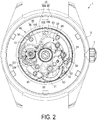
- FIG. 2 is a plan view of the mechanical watch 1 according to the first embodiment as viewed from the case back side. Note that, regarding screws 90 for securing the components of the watch, only some of them are designated with the reference sign.
- the mechanical watch 1 has a see-through structure in which a part of a movement 40 is visible from the dial side or the case back side.
- a plan view of the mechanical watch 1 as viewed from the dial side is described with reference to FIGS. 1 and 2 .
- the mechanical watch 1 includes a cylindrical outer case 5, and a disk-shaped dial 3 is disposed on an inner circumferential side of the outer case 5.
- a window 48A is provided in the dial 3.
- the mechanical watch 1 is configured such that a part of the movement 40 is visible through the window 48A.
- the opening on the front side is covered with a cover glass, and a case back 35 is attached to the opening on the rear side.
- the mechanical watch 1 includes a movement 40 housed in the outer case 5, an hour hand 44A that indicates time information, a minute hand 44B, a power reserve hand 44C that indicates mainspring duration, and a small second 44D.
- the watch hand 44A, the minute hand 44B, the power reserve needle 44C, and the small second 44D are attached to a hand shaft of the movement 40 and are driven by the movement 40.
- a crown 7 is provided on a side surface of the outer case 5. By operating the crown 7, an input corresponding to the operation can be made.
- an escape wheel 101 In FIG. 1 , an escape wheel 101, an anchor 28, a balance wheel 27, a balance spring 29 and the like that constitute a part of the movement 40 are visible from the dial side through the window 48A provided in the dial 3.
- the escape wheel 101 includes a shaft member 102 and the escape gear wheel part 100 as the watch component according to the first embodiment.
- FIGS. 1 and 2 A plan view of the mechanical watch 1 as viewed from the case back side is described with reference to FIGS. 1 and 2 .
- the case back 35 is composed of a ring-shaped frame material 46 defining an outer peripheral portion, and a window 48B made of a transparent member fitted to the frame material 46.
- the movement 40 includes a wheel train 45, a balance bridge 13, a manual winding mechanism 60, an automatic winding mechanism 50, and the like.
- the wheel train 45 includes a barrel 21, a center wheel, a third wheel, a fourth wheel 51, the escape wheel 101, the anchor 28, the balance wheel 27 and the like provided on the case back side of the main plate.
- FIG. 2 illustrates the barrel 21, the fourth wheel 51, the escape wheel 101, the anchor 28 and the balance wheel 27.
- the escape wheel 101 and the anchor 28 constitute an escapement 80, and the balance wheel 27 and the balance spring 29 constitute a speed governor 70.
- the manual winding mechanism 60 includes a stem, a winding wheel, a clutch wheel, a crown wheel 61, a ratchet transmission wheel 62, a ratchet wheel 63, and the like.
- FIG. 2 illustrates the crown wheel 61, the ratchet transmission wheel 62, and the ratchet wheel 63.
- the automatic winding mechanism 50 includes a rotation weight, a bearing, an eccentric wheel, a claw lever, a transmission wheel 52, and the like.
- FIG. 2 illustrates the transmission wheel 52.
- the barrel 21, the escape wheel 101, the anchor 28, the balance wheel 27, the crown wheel 61, the ratchet transmission wheel 62, the ratchet wheel 63, the eccentric wheel, the transmission wheel 52 and the like that constitute a part of the movement 40 are visible from the case back side through the window 48B provided in the case back 35.
- the aspect for visual recognition of components of the movement 40 from the dial side or the case back side is not limited to the above-described aspect.
- the design, size, arrangement position, number of windows, and the like of the windows 48A and 48B may be appropriately changed such that desired components of the movement 40 are visible.
- the entirety of the dial 3 may be formed with a transparent member such that the entirety of the movement 40 is visible from the dial side
- the entirety of the case back 35 may be formed with a transparent member such that the entirety of the movement 40 is visible from the case back side.
- FIG. 3 is a plan view of the escape gear wheel part 100 according to the first embodiment.
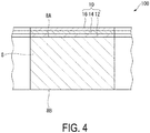
- FIG. 4 is a partial cross-sectional view taken along the line A-A of FIG. 3 .
- the escape gear wheel part 100 of the first embodiment includes a base member 8 mainly composed of silicon.
- the base member 8 includes a first surface 8A and a second surface 8B opposite the first surface 8A.
- a light reflecting layer 10 having a three-layer structure in which a first silicon oxide layer 12, a silicon layer 14, and a second silicon oxide layer 16 are layered in this order is provided on the first surface 8A of the base member 8.
- the first surface of the base member means a surface on the side from which the watch component is visible when the watch component is mounted in the watch.
- the first surface of the base member means the surface located on the case back side of the watch. Note that, in the case where the watch component is visible from both the case back side and the dial side of the watch, the first surface of the base member is the surface located on the dial side of the watch.
- the escape gear wheel part 100 as the watch component is visible from both the case back side and the dial side of the mechanical watch 1, and therefore the first surface 8A of the base member 8 is the surface located on the dial side, and the second surface 8B of the base member 8 is the surface located on the case back side.
- the base member means a watch component of a state in which no light reflecting layer is formed.
- the base member 8 means an escape gear wheel part of a state in which the light reflecting layer 10 is not formed.
- mainly composed of silicon means that the content of silicon of the entire base member is 80 mass% or greater.
- the content of the silicon is preferably 90 mass% or greater, more preferably 95 mass% or greater.
- the base member 8 mainly composed of silicon may be referred to as the base member 8 made of silicon.
- the base member 8 is mainly composed of silicon.
- the type of silicon is not limited, and may be appropriately selected from the perspective of processability.
- Examples of the silicon include monocrystalline silicon and polycrystalline silicon. They may be used alone or in combination.
- the base member 8 made of silicon can be manufactured by, for example, a photolithography technique and an etching technique, and thus a complex shape can be formed.
- the light reflecting layer 10 has a three-layer structure in which the first silicon oxide layer 12, the silicon layer 14, and the second silicon oxide layer 16 are layered in this order on the first surface 8A of the base member 8.
- the light reflecting layer 10 has a function of freely adjusting transmission and/or reflection of light at least at one of a surface of the second silicon oxide layer 16 opposite the silicon layer 14, an interface between the second silicon oxide layer 16 and the silicon layer 14, an interface between the silicon layer 14 and the first silicon oxide layer 12, and the first surface 8A of the base member 8.
- the outermost layer of the light reflecting layer 10 is the second silicon oxide layer 16.
- the protection of the escape gear wheel part 100 is enhanced.
- the average thickness of the light reflecting layer 10 is adjusted in accordance with the coloring, the average thickness is preferably from 265nm to 885nm from the perspective of productivity.
- a first silicon oxide layer 12 is provided on the first surface 8A of the base member 8.
- the average thickness of the first silicon oxide layer 12 is adjusted in accordance with the coloring, the average thickness of the first silicon oxide layer 12 is typically from 100nm to 450nm, and is preferably from 100nm to 400nm. When the average thickness of the first silicon oxide layer 12 is 100nm or greater, the thickness can be easily controlled. When the average thickness of the first silicon oxide layer 12 is 400nm or smaller, the film formation time can be shortened, and as a result the productivity is improved.
- the average thickness of the first silicon oxide layer 12 is preferably from 20nm to 100nm, or from 180nm to 290nm, or, 330nm or greater, more preferably from 210nm to 280nm.
- the upper limit value is preferably 450nm or smaller from the perspective of productivity.
- a proper range of the average thickness of the first silicon oxide layer 12 can be calculated, for example, by the optical calculation described in the Examples described later.
- the first silicon oxide layer 12 is preferably a thermally oxidized silicon layer formed by a thermal oxidation method.
- a thermal oxidation method When the thermally oxidized silicon layer 12 is formed by a thermal oxidation method, a silicon layer with high uniformity can be easily obtained. Thus, the escape gear wheel part 100 is more easily colored with the same color.
- the silicon layer 14 is provided on the first silicon oxide layer 12.
- the average thickness of the silicon layer 14 is preferably from 66nm to 86nm.
- the average thickness of the silicon layer 14 is from 66nm to 86nm, the color is easily controlled.
- the average thickness of the silicon layer 14 is more preferably from 70nm to 84nm from the perspective of suppressing the coloring difference depending on the observation angle.
- a preferred range of the average thickness of the silicon layer 14 can be calculated, for example, by the optical calculation described in the Examples described later.
- the silicon layer 14 may be an amorphous layer or a polysilicon layer, the silicon layer 14 is preferably a polysilicon layer.
- the second silicon oxide layer 16 is provided on the silicon layer 14.
- the average thickness of the second silicon oxide layer 16 is from 100nm to 200nm, or from 250nm to 360nm, or, 400nm or greater, more preferably, from 130nm to 200nm, or from 310nm to 360nm from the perspective of reducing the coloring difference depending on the observation angle.
- the upper limit value is preferably 500nm or smaller from the perspective of productivity.
- a proper range of the average thickness of the second silicon oxide layer 16 can be calculated, for example, by the optical calculation described in the Examples described later.
- the second silicon oxide layer 16 is preferably a thermally oxidized silicon layer formed by a thermal oxidation method. Since the thermally oxidized silicon layer typically has a mechanical property superior to the silicon oxide layer formed by a vapor deposition method, the protecting property of the base member 8 is further enhanced when the second silicon oxide layer 16 is composed of a thermally oxidized silicon layer. In particular, it is particularly desirable for a gear, such as the escape gear wheel part 100, having a portion that makes contact with other parts since the mechanical strength of the contact portion is enhanced.
- the average thickness of the second silicon oxide layer 16 is adjusted in accordance with the coloring, the average thickness of the second silicon oxide layer 16 is preferably smaller than the average thickness of the first silicon oxide layer 12.
- a silicon layer formed prior to formation of the second silicon oxide layer 16 is oxidized to form the second silicon oxide layer 16, for example.
- the silicon layer is composed of an amorphous layer or a polysilicon layer, it is difficult to control the thickness of the second silicon oxide layer 16.
- the layer thickness of the second silicon oxide layer 16 is preferably thin since the smaller the layer thickness, the easier the layer thickness control. Therefore, the average thickness of the second silicon oxide layer 16 is preferably smaller than the average thickness of the first silicon oxide layer 12.
- the average thicknesses of the first silicon oxide layer 12, the silicon layer 14, and the second silicon oxide layer 16 can be measured by the following method.
- a portion of the escape gear wheel part 100 as a watch component is cut out and used as a test piece.
- the cross section of the test piece is observed using a SEM (scanning electron microscope), the thickness of the measurement object layer is measured at arbitrary ten points, and the average value thereof is used as the "average thickness of the measurement object layer".
- the measurement object layer is any of the first silicon oxide layer 12, the silicon layer 14, and the second silicon oxide layer 16.
- the escape gear wheel part 100 of the first embodiment includes the light reflecting layer 10 in which a silicon oxide layer, which is a relatively low refractive index layer, and a silicon layer, which is a relatively high refractive index layer, are alternately stacked in three layers on the first surface 8A of the base member 8 made of silicon, and thus can be decorated with favorable coloring in comparison with the case where one silicon oxide layer is layered on the first surface 8A of the base member 8. As a result, the escape gear wheel part 100 having excellent decorativeness is achieved.
- each layer of the light reflecting layer 10 is composed of a material including silicon in the escape gear wheel part 100, the adhesion between the base member 8 and the first silicon oxide layer 12 and the adhesion between each layer of the light reflecting layer 10 are conceivably favorable. As a result, the adhesive layer that is typically provided between the base member 8 and the light reflecting layer 10 is unnecessary, and the durability of the structure is improved in its entirety.
- the escape gear wheel part 100 has a structure in which the protective property of the base member 8 is enhanced.
- a physically and chemically stable second silicon oxide layer 16 can also provide a function as a protective material for the base member 8.
- All of the base member 8 and the light reflecting layer 10 include silicon and the escape gear wheel part 100 can be decorated with favorable coloring, and thus, the escape gear wheel part 100 has a configuration that does not exist in the related art.
- a desired color can be given to the escape gear wheel part 100 of the first embodiment by adjusting the average thickness of each layer of the light reflecting layer 10.
- Examples of the desired color include, but not limited to, blue, green, red, yellow, pink, blue-green, and other mixed colors.
- the maximum reflectance in the range from 400nm to 780nm with light incident on the light reflecting layer 10 at an incident angle of 0° is preferably 50% or greater, more preferably 60% or greater, still more preferably 70% or greater.
- the incident angle of 0° is the angle of the incident light with respect to the direction of the normal to the light reflecting layer.
- the maximum reflectance of the escape gear wheel part 100 can be measured using a test piece under the following condition.
- the escape gear wheel part 100 itself or a piece of the escape gear wheel part 100 cut into a measurable size may be used as the test piece in accordance with the specification of the measurement device.
- the maximum reflectance in the case where the escape gear wheel part 100 is colored blue is preferably 50% or greater, more preferably 60% or greater, still more preferably 70% or greater in the range from 400nm to 550nm.
- the maximum reflectance in the case where the escape gear wheel part 100 is colored red is preferably 50% or greater, more preferably 60% or greater, still more preferably 70% or greater in the range of 600nm to 800nm.
- the maximum reflectance in the case where the escape gear wheel part 100 is colored green is preferably 50% or greater, more preferably 60% or greater, still more preferably 70% or greater in the range from 400nm to 600nm.
- the escape gear wheel part 100 be colored a mixed color such as a blue green color and a pink color.
- the method for manufacturing the escape gear wheel part 100 of the first embodiment includes forming the light reflecting layer 10 having a three-layer structure in which the first silicon oxide layer 12, the silicon layer 14, and the second silicon oxide layer 16 are layered in this order on the first surface 8A of the base member 8 made of silicon.
- the escape gear wheel part 100 having excellent decorativeness is manufactured.
- the step of forming the light reflecting layer 10 includes a step of forming the first silicon oxide layer 12 on the first surface 8A of the base member 8, a step of forming the silicon layer 14 on the first silicon oxide layer 12, and a step of forming the second silicon oxide layer 16 on the silicon layer 14.
- the base member 8 may be manufactured, or may be an available product.
- the base member 8 can be manufactured by, for example, a photolithography technique and an etching technique.
- the base member 8 made of silicon the weight reduction of the escape gear wheel part 100 is achieved in comparison with the case where a metal base member is used.
- complex shapes can be formed by a photolithography technique and an etching technique.
- Examples of the method of forming the first silicon oxide layer 12 include a thermal oxidation method, a physical vapor deposition (PVD) method, a chemical vapor deposition (CVD) method, and combinations thereof.
- thermal oxidation method examples include a wet oxidation method using water and a dry oxidation method using oxygen.
- Examples of the PVD method include a sputtering method, an ion plating method, and a vacuum deposition method.
- Examples of the CVD method include a plasma chemical vapor deposition method, a thermal chemical vapor deposition method, and a photochemical vapor deposition method.
- the method of forming the first silicon oxide layer 12 is preferably a thermal oxidation method using water or a dry oxidation method using oxygen.
- the first silicon oxide layer 12 is formed by a thermal oxidation method
- a vertical or a horizontal thermal oxidation furnace is preferably used from the perspective of productivity.
- the forming condition of the first silicon oxide layer 12 are appropriately adjusted in accordance with the shape of the base member 8, the intended thickness, and the like.
- Examples of the method of forming the silicon layer 14 include a PVD method, a CVD method, and combinations thereof.
- Examples of the PVD method and the CVD method include methods similar to those described for the step of forming the first silicon oxide layer 12.
- the silicon layer 14 is preferably formed by a low-pressure CVD method.
- the silicon layer 14 can be formed at least on the first surface 8A of the base member 8 by feeding monosilane gas under low pressure while controlling the deposition temperature at a temperature from 500°C to 700°C.
- the layer quality of the silicon layer can be controlled from amorphous silicon to polysilicon in accordance with the deposition temperature.
- a vertical or horizontal low-pressure CVD furnace is preferably used from the perspective of productivity.
- the forming conditions of the silicon layer 14 are appropriately adjusted in accordance with the shape of the base member 8, the intended thickness, and the like.
- Examples of the method of forming the second silicon oxide layer 16 include methods similar to the methods of forming the first silicon oxide layer 12, and the same applies to the preferable method thereof.
- the second silicon oxide layer 16 is preferably formed by thermally oxidizing a portion of the silicon layer 14, as in Example 7 described later. As a result, conceivably, the function as a protective material of the second silicon oxide layer 16 is further presented.
- the forming conditions of the second silicon oxide layer 16 are appropriately adjusted in accordance with the shape of the base member 8, the intended thickness, and the like.
- the manufacturing method of the first embodiment it is preferable to form at least one of the first silicon oxide layer 12 and the second silicon oxide layer 16 by a thermal oxidation method, and it is more preferable to form both the first silicon oxide layer 12 and the second silicon oxide layer 16 by a thermal oxidation method.
- An escape gear wheel part according to the second embodiment is the same as the escape gear wheel part 100 according to the first embodiment except that a light reflecting layer having a three-layer structure in which a first silicon oxide layer, a silicon layer, and a second silicon oxide layer are layered in this order is provided on the second surface of the base member.
- FIG. 5 is a partial cross-sectional view of an escape gear wheel part 200 according to the second embodiment, and specifically is a partial cross-sectional view taken along the line A-A on the assumption that the light reflecting layer 10 is provided also on the second surface 8B of the base member 8 in the escape gear wheel part 100 of FIG. 3 .
- the escape gear wheel part 200 includes the light reflecting layers 10 and 20 having three-layer structures in which the first silicon oxide layers 12 and 22, the silicon layers 14 and 24, and the second silicon oxide layers 16 and 26 are layered in this order on the first surface 8A and the second surface 8B of the base member 8.
- the average thicknesses of the first silicon oxide layer 22, the silicon layer 24, and the second silicon oxide layer 26 in the second embodiment may be identical to or different from the first silicon oxide layer 12, the silicon layer 14, and the second silicon oxide layer 16, respectively, the average thicknesses are preferably identical from the perspective of reducing the distortion of the base member 8 due to the layer stresses of the light reflecting layers 10 and 20.
- the stress of the stacked layer often causes problems.
- the thickness of the base member is of the order of 100 ⁇ m in a gear such as the escape gear wheel part, and as such, in the case where the light reflecting layer is formed on only one surface of the gear, the gear may distort due to the stress of the light reflecting layer.
- the escape gear wheel part 200 of the second embodiment reduces the distortion of the base member 8 due to the layer stresses of the light reflecting layers 10 and 20.
- the second silicon oxide layers 16 and 26 provided at the outermost layer enhance the protective property of each of the first surface 8A and the second surface 8B of the base member 8. As a result, the escape gear wheel part 200 with more excellent durability is achieved.
- the escape gear wheel part 200 is mounted in the mechanical watch 1 having a see-through structure such as that illustrated in FIGS. 1 and 2 , the escape gear wheel part 200 is visible from both the case back side and the dial side, and thus the decorativeness of the mechanical watch 1 can be further improved.
- the escape gear wheel part 200 of the second embodiment is effective in enhancing the decorativeness of the mechanical watch 1.
- the method for manufacturing the escape gear wheel part 200 of the second embodiment is the same as the manufacturing method of the first embodiment except that a step of forming the light reflecting layer 20 is further provided in addition to the manufacturing method of the first embodiment.
- the light reflecting layer 20 can be formed in the same manner as the light reflecting layer 10 in the first embodiment.
- the escape gear wheel part 200 of the second embodiment is preferably manufactured by simultaneously forming the first silicon oxide layers 12 and 22 on the first surface 8A and the second surface 8B of the base member 8, and then simultaneously forming the silicon layers 14 and 24, and then, simultaneously forming the second silicon oxide layers 16 and 26.
- Examples of the simultaneous forming method include a method the layers of the light reflecting layers 10 and 20 are simultaneously formed while only the outer periphery of the base member 8 is placed on a boat in a vertical or horizontal furnace.
- the average thicknesses of the first silicon oxide layers 12 and 22, the silicon layers 14 and 24, and the second silicon oxide layers 16 and 26 are set to substantially the same average thickness, and thus the escape gear wheel part 200 that suppresses the distortion of the base member 8 due to the layer stress of the light reflecting layers 10 and 20 is obtained.
- the escape gear wheel part 200 using the base member 8 made of silicon tends to be brittle in comparison with an escape gear wheel part using a metal base member, and therefore it is generally difficult to form the light reflecting layers 10 and 20 on the first surface 8A and the second surface 8B of the base member 8 in terms of device conveyance and handleability.
- the base member 8 when a vertical or horizontal furnace is used to form the light reflecting layers 10 and 20, the base member 8 can be set by hand insertion, and therefore, even when the base member 8 is brittle, each of the first silicon oxide layers 12 and 22, the silicon layers 14 and 24, and the second silicon oxide layers 16 and 26 can be formed on the first surface 8A and the second surface 8B of the base member 8 in a single formation. In addition, this method can reduce the number of steps by one-half.
- At least one of the first silicon oxide layers 12 and 22 and the second silicon oxide layers 16 and 26 is preferably formed by a thermal oxidation method, and the silicon layers 14 and 24 is preferably formed by a low-pressure CVD method.
- An escape gear wheel part according to the third embodiment is the same as the escape gear wheel part 200 according to the second embodiment except that a light reflecting layer having a three-layer structure in which a first silicon oxide layer, a silicon layer, and a second silicon oxide layer are layered in this order on the side surface where the first surface and the second surface of the base member are coupled.
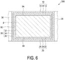
- FIG. 6 is a partial cross-sectional view of an escape gear wheel part 300 according to the third embodiment, and specifically is a partial cross-sectional view taken along the line A-A on the assumption that the light reflecting layer 10 is provided also on the second surface 8B and a side surface 8C of the base member 8 in the escape gear wheel part 100 illustrated in FIG. 3 .
- the escape gear wheel part 300 includes the light reflecting layers 10, 20 and 30 having a three-layer structures in which first silicon oxide layers 12, 22 and 32, silicon layers 14, 24 and 34, and second silicon oxide layers 16, 26 and 36 are layered in this order on the first surface 8A, the second surface 8B, and the side surface 8C of the base member 8.
- the light reflecting layers 10, 20 and 30 are provided on the first surface 8A, the second surface 8B, and the side surface 8C of the base member 8, or in other words, the light reflecting layers 10, 20 and 30 are provided on the entire surface of the base member 8, the distortion of the base member 8 is further suppressed and the protective property of the base member 8 in its entirety is enhanced. As a result, the escape gear wheel part 300 with more excellent durability is achieved.
- the contact portion is protected by the light reflecting layer 30 covering the side surface 8C of the base member 8, and thus the breaking resistance of the gear can be improved.
- the method for manufacturing the escape gear wheel part 300 of the third embodiment is the same as the manufacturing method of the second embodiment except that a step of forming the light reflecting layer 30 is further provided in addition to the manufacturing method of the second embodiment.
- the light reflecting layer 30 can be formed in the same manner as the light reflecting layer 10 in the first embodiment.
- the escape gear wheel part 300 of the third embodiment is preferably manufactured by simultaneously forming the first silicon oxide layers 12, 22 and 32 on the first surface 8A, the second surface 8B, and the side surface 8C of the base member 8, and then simultaneously forming the silicon layers 14, 24 and 34, and then, simultaneously forming the second silicon oxide layers 16, 26 and 36.
- Examples of the simultaneous forming method include a method in which the layers of the light reflecting layers 10, 20 and 30 are simultaneously formed while only the outer periphery of the base member 8 is placed on a boat in a vertical or horizontal furnace in the same manner as the second embodiment.
- the average thicknesses of the first silicon oxide layers 12, 22 and 32, the silicon layers 14, 24 and 34, and the second silicon oxide layers 16, 26 and 36 are set to substantially the same average thickness, and thus the escape gear wheel part 300 that suppresses the distortion of the base member 8 due to the layer stress of the light reflecting layers 10, 20 and 30 is obtained.
- At least one of the first silicon oxide layers 12, 22 and 32 and the second silicon oxide layers 16, 26 and 36 is preferably formed by a thermal oxidation method, and the silicon layers 14 and 24, 36 is preferably formed by a low-pressure CVD method.
- escape gear wheel part 100 as a watch component and the mechanical watch 1 provided with the escape gear wheel part 100 are described in the above-described embodiments, the present disclosure is not limited thereto.
- the mechanical watch 1 according to the first embodiment is provided with at least one watch component of the present disclosure.
- the escape gear wheel part 100 may have an antistatic layer or a soil-resistant layer having transparency at the outermost layer to the extent that the decorativeness is not impaired.
- a soil-resistant function or an antistatic function is provided to the escape gear wheel part 100.
- any desired step can be added as necessary.
- an intermediate process such as washing may be performed between each step.
- a step of forming a soil-resistant layer or a step of forming an anti-static layer may be performed.
- a preprocess such as cutting, grinding, polishing, and honing may be provided to the base member.
- the watch movement according to this embodiment includes at least one of the watch components according to the above-described embodiments. According to this embodiment, a watch movement with excellent decorativeness and high design property is achieved.
- the watch according to this embodiment includes at least one of the watch components according to the above-described embodiments.
- the watch is not limited, and examples of the watch include a quartz watch, a mechanical watch, and an electronically controlled mechanical watch. Among them, from the perspective of presenting more decorativeness of the watch component, it is preferable that the watch be a mechanical watch with a see-through structure.
- the reflection spectrum with a change in thickness of the first silicon oxide layer was determined by calculation using the refractive index n and the extinction coefficient k of each of the silicon base member and the first silicon oxide layer at a wavelength from 400nm to 800nm.
- the reflectance R ( ⁇ ) and the color-matching function illustrated in FIG. 7 were converted to the three stimulus values XYZ by using the following Equations (1A) to (1C) and Equation (2), and then converted to RGB values of a 256-level gradation by using the following Equation (3) and Equations (4A) to (4C).
- a graph of the relationship between the thickness of the silicon oxide layer and the gradation was created based on the RGB value.
- the created graph is illustrated in FIG. 8 .
- a silicon base member may be referred to as an "Si base member", a first silicon oxide layer as a “first SiO 2 layer”, a silicon layer as an “Si layer”, and a second silicon oxide layer as a "second SiO 2 layer”.
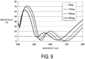
- a laminate in which a light reflecting layer including a first silicon oxide layer of 220nm, a silicon layer of 76nm, and a second silicon oxide layer of 140nm is formed on the silicon base member was used as the watch component 1.
- the observation angle was changed to 0°, 15°, 30° and 45°, and the reflection spectrum was determined for each observation angle.
- the determined reflection spectrum was converted to an RGB value of the 256-level gradation in the above-described method.
- the reflection spectrum in the case where the thicknesses of the first SiO 2 layer, the Si layer, and the second SiO 2 layer were changed was calculated using the refractive index n and the extinction coefficient k of each of the Si base member, the first SiO 2 layer, the Si layer, and the second SiO 2 layer at a wavelength from 400nm to 800nm (see FIG. 9 ). Subsequently, the reflection spectrum was converted to an RGB gradation of the 256-level gradation in a manner similar to the above-described method.
- FIG. 9 is a graph of the relationship between the wavelength and the reflectance of the watch component 1.
- a reflectance of 70% at maximum is indicated in a blue region of a wavelength from 400nm to 550nm, and that the reflectance can be limited to approximately 20% in a wavelength region of approximately from 550nm to 750nm.
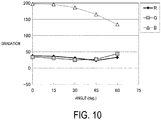
- FIG. 10 illustrates the relationship between the observation angle and the gradation of the watch component 1.
- Si Base member/first SiO 2 layer from 10nm to 500nm
- Si layer 76nm
- second SiO 2 layer 140nm
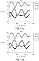
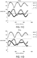
- FIGS. 11A to 11D are graphs of the relationship between the thickness of the first silicon oxide layer and the gradation at observation angles of 0°, 15°, 30° and 45° in the watch component 2.
- the thickness of the first silicon oxide layer is preferably from 20nm to 100nm, or from 180 to 290nm, or, from 330nm to 500nm.
- the thickness of the first silicon oxide layer is more preferably from 210nm to 280nm.
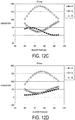
- FIGS. 12A to 12D are graphs of the relationship between the thickness of the silicon layer and the gradation at observation angles of 0°, 15°, 30° and 45° in the watch component 3.
- the thickness of the silicon layer is preferably from 66nm to 86nm. Further, also considering the observation angle of 45°, it is shown that the thickness of the silicon layer is more preferably from 70nm to 84nm.
- FIGS. 13A to 13D are graphs of the relationship between the thickness of the second silicon oxide layer and the gradation at observation angles of 0°, 15°, 30° and 45° in the watch component 4.
- the thickness of the second silicon oxide layer is preferably from 100nm to 200nm, or from 250nm to 360nm, or, from 400nm to 550nm. Further, also considering the observation angle of 45°, it is shown that the thickness of the second silicon oxide layer is more preferably from 130nm to 200nm, or from 310nm to 360nm.
- a laminate in which a light reflecting layer including a first silicon oxide layer of 150nm, a silicon layer of 110nm, and a second silicon oxide layer of 70nm are formed on a silicon base member was used as a watch component 5.
- FIG. 14 is a graph illustrating the relationship between the wavelength and the reflectance in the watch component 5.
- a reflectance of 70% at maximum is indicated in a red region of a wavelength from 600nm to 800.
- FIG. 15 illustrates the relationship between the observation angle and the gradation of the watch component 5.
- R was increased to approximately 250 gradation level
- B and G were at approximately 100 gradation or lower.
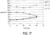
- a laminate in which a light reflecting layer including a first silicon oxide layer of 330nm, a silicon layer of 76nm, and a second silicon oxide layer of 140nm are formed on a silicon base member was used as a watch component 6.
- the watch component 6 is an example of the watch component 2.
- FIG. 16 is a graph of the relationship between the wavelength and the reflectance of the watch component 6.
- FIG. 17 illustrates the relationship between the observation angle and the gradation of the watch component 6.
- a silicon wafer was prepared, and a photoresist was applied to one surface of the silicon wafer by a spin coating method while the back-surface mask material was disposed on the other surface, and, the photoresist and the back-surface mask material were cured.
- the photoresist was then exposed by photolithography, followed by development to form a photoresist pattern corresponding to the planar outer shape of the base member of the escape gear wheel.
- the silicon wafer was then etched with a photoresist pattern as a mask to form an outer shape of the base member of the escape gear wheel part including a projecting portion, an elastic portion, and a rim portion.
- the base member of the escape gear wheel part was placed in a vertical thermal oxidation furnace and held for 17 minutes after heating to 1050°C.
- a first SiO 2 layer having a thickness of 220nm was formed on the entire surface, namely, the first surface, the second surface, and the side surface, of the base member, and thus a laminate 1 (base member/first SiO 2 layer (220nm)) was obtained.
- the outer periphery of the laminate 1 (base member/first SiO 2 layer (220nm)) was placed on a claw of a quartz boat.
- the furnace was depressurized with a dry pump and the base member was heated to 625°C.
- the monosilane gas was then fed for 19 minutes and 30 seconds.
- the laminate 2 (base member/first SiO 2 layer (220nm)/Si layer (138nm)) was placed in a vertical thermal oxidation furnace and held for 33 minutes after heating to 950°C.
- the second SiO 2 layer was formed through thermal oxidation of the Si layer of the laminate 2.
- the Si layer of the laminate 2 is consumed by approximately 44.6%. Accordingly, the Si layer of the laminate 2 was consumed by approximately 62nm so as to be 76nm.
- the average thicknesses of the first silicon oxide layer, the silicon layer, and the second silicon oxide layer were measured by the above-described method.
- the average thicknesses of the first silicon oxide layer, the silicon layer, and the second silicon oxide layer measured by the above-described method match the thicknesses of the first silicon oxide layer, the silicon layer, and the second silicon oxide layer that were aimed in Example 7.
- the escape gear wheel part exhibited a blue color with favorable coloring at each of the observation angles of 0°, 15°, 30° and 45°.
Landscapes
- Physics & Mathematics (AREA)
- General Physics & Mathematics (AREA)
- Gears, Cams (AREA)
- Engineering & Computer Science (AREA)
- Manufacturing & Machinery (AREA)
- Metallurgy (AREA)
Abstract
Description
- The present application is based on, and claims priority from
JP Application Serial Number 2019-046905, filed March 14, 2019 - The present disclosure relates to a watch component, a watch movement, and a watch.
- While watch components have been formed by machining a metal material in the related art, a base member containing silicon has been used in recent years as a material for watch components from the perspective of weight reduction and processability.
- In addition, in recent years, decorativeness is desired not only for the watch components that are exposed to the outside of the watch, but also for the watch components incorporated inside the watch.
- For example,
JP-A-2016-114407 - For the watch with the see-through structure disclosed in
JP-A-2016-114407 - A watch component of the present disclosure includes: a base member including a first surface and a second surface opposite the first surface, the base member being mainly composed of silicon; and a light reflecting layer provided at the first surface of the base member, the light reflecting layer having a three-layer structure in which a first silicon oxide layer, a silicon layer, and a second silicon oxide layer are layered in this order.
- In the watch component of the present disclosure, an average thickness of the second silicon oxide layer may be smaller than an average thickness of the first silicon oxide layer.
- In the watch component of the present disclosure, an average thickness of the silicon layer may be from 66nm to 86nm.
- In the watch component of the present disclosure, an average thickness of the first silicon oxide layer may be from 100nm to 400nm.
- In the watch component of the present disclosure, a light reflecting layer having a three-layer structure in which a first silicon oxide layer, a silicon layer, and a second silicon oxide layer are layered in this order may be further provided at the second surface of the base member.
- In the watch component of the present disclosure, a light reflecting layer having a three-layer structure in which a first silicon oxide layer, a silicon layer, and a second silicon oxide layer are layered in this order may be further provided at a side surface where the first surface and the second surface are coupled.
- In the watch component of the present disclosure, a maximum reflectance for light having a wavelength in a range from 400nm to 780nm when the light is incident on the light reflecting layer at an incident angle of 0° may be 50% or greater.
- In the watch component of the present disclosure, the watch component may be at least one selected from the group consisting of a barrel, a wheel, an escape wheel, an anchor, and a balance.
- A method for manufacturing a watch component of the present disclosure includes forming a light reflecting layer at a first surface of a base member including the first surface and a second surface opposite the first surface, the base member being mainly composed of silicon, the light reflecting layer having a three-layer structure in which a first silicon oxide layer, a silicon layer, and a second silicon oxide layer are layered in this order.
- In the above-mentioned method of the present disclosure, at least one of the first silicon oxide layer and the second silicon oxide layer may be formed by a thermal oxidation method.
- In the above-mentioned method of the present disclosure, the silicon layer may be formed by a low-pressure CVD method.
- A watch movement of the present disclosure includes the above-mentioned watch component.
- A watch of the present disclosure includes the above-mentioned watch component.
- The watch of the present disclosure may be a mechanical watch having a see-through structure.
-
-
FIG. 1 is a plan view of a mechanical watch according to a first embodiment as viewed from the dial side. -
FIG. 2 is a plan view of the mechanical watch according to the first embodiment as viewed from the case back side. -
FIG. 3 is a plan view of an escape gear wheel part according to the first embodiment. -
FIG. 4 is a schematic cross-sectional view taken along the line A-A ofFIG. 3 . -
FIG. 5 is a partial cross-sectional view of an escape gear wheel part according to a second embodiment, and specifically is a partial cross-sectional view taken along the line A-A on the assumption that a light reflecting layer is also provided on a second surface of a base member in the escape gear wheel part illustrated inFIG. 3 . -
FIG. 6 is a partial cross-sectional view of the escape gear wheel part according to the third embodiment, and specifically is a partial cross-sectional view taken along the line A-A on the assumption that a light reflecting layer is also provided on a second surface and a side surface of a base member in the escape gear wheel part illustrated inFIG. 3 . -
FIG. 7 is a graph of a color-matching function. -
FIG. 8 is a graph of a relationship between the thickness and the gradation of a silicon oxide layer when one silicon oxide layer is formed on a silicon base member. -
FIG. 9 is a graph of a relationship between the wavelength and the reflectance of awatch component 1 of Example 1. -
FIG. 10 is a graph of a relationship between the observation angle and the gradation of thewatch component 1 of Example 1. -
FIG. 11A is a graph of a relationship between the gradation and the thickness of a first silicon oxide layer at an observation angle of 0° in awatch component 2 of Example 2. -
FIG. 11B is a graph of a relationship between the gradation and the thickness of the first silicon oxide layer at an observation angle of 15° in thewatch component 2 of Example 2. -
FIG. 11C is a graph of a relationship between the gradation and the thickness of the first silicon oxide layer at an observation angle of 30° in thewatch component 2 of Example 2. -
FIG. 11D is a graph of a relationship between the gradation and the thickness of the first silicon oxide layer at an observation angle of 45° in thewatch component 2 of Example 2. -
FIG. 12A is a graph of a relationship between the gradation and the thickness of a silicon layer at an observation angle of 0° in awatch component 3 of Example 3. -
FIG. 12B is a graph of a relationship between the gradation and the thickness of the silicon layer at an observation angle of 15° in thewatch component 3 of Example 3. -
FIG. 12C is a graph of a relationship between the gradation and the thickness of the silicon layer at an observation angle of 30° in thewatch component 3 of Example 3. -
FIG. 12D is a graph of a relationship between the gradation and the thickness of the silicon layer at an observation angle of 45° in thewatch component 3 of Example 3. -
FIG. 13A is a graph of a relationship between the gradation and the thickness of a second silicon oxide layer at an observation angle of 0° in awatch component 4 of Example 4. -
FIG. 13B is a graph of a relationship between the gradation and the thickness of the second silicon oxide layer at an observation angle of 15° in thewatch component 4 of Example 4. -
FIG. 13C is a graph of a relationship between the gradation and the thickness of the second silicon oxide layer at an observation angle of 30° in thewatch component 4 of Example 4. -
FIG. 13D is a graph of a relationship between the gradation and the thickness of the second silicon oxide layer at an observation angle of 45° in thewatch component 4 of Example 4. -
FIG. 14 is a graph of a relationship between the wavelength and the reflectance of awatch component 5 of Example 5. -
FIG. 15 is a graph of a relationship between the observation angle and the gradation of thewatch component 5 of Example 5. -
FIG. 16 is a graph of a relationship between the wavelength and the reflectance of a watch component 6 of Example 6. -
FIG. 17 is a graph of a relationship between the observation angle and the gradation of the watch component 6 of Example 6. - A watch component of the present disclosure is a concept that includes a watch interior component, and a screw for securing watch components, in addition to a watch exterior component exposed to the outside of a watch.
- Examples of the watch exterior part include a watch case, a watch band, a dial, a watch hand, a bezel, a crown, a button, a cover glass, a glass edge, a dial ring, a panel cover and a packing. Examples of the watch case include a body, a case back, and a one-piece case where the body and the case back are integrated. Examples of the watch band include a band clasp, a part used for attaching and detaching the band, and a part used for attaching and detaching a bangle. Examples of the bezel include a rotating bezel. Examples of the crown include a thread-locking crown.
- Examples of the watch interior component include a barrel, a wheel, an escape wheel, an anchor, a balance and a mainspring.
- Among them, from the perspective of presenting more decorativeness, the watch component is preferably a watch interior component, more preferably at least one selected from the group consisting of a barrel, a wheel, an escape wheel, an anchor, and a balance.
- In other words, from the perspective of presenting more decorativeness, the watch component is preferably mounted in a watch of a see-through structure whose inner mechanism is visible.
- A first embodiment of the present disclosure is described below with reference to the accompanying drawings.
- In the first embodiment, an escape gear wheel part constituting an escape wheel is described as an example of a watch component. A mechanical watch is described as an example of a watch provided with the escape gear wheel part.
-
FIG. 1 is a plan view illustrating amechanical watch 1 according to the first embodiment as viewed from the dial side.FIG. 2 is a plan view of themechanical watch 1 according to the first embodiment as viewed from the case back side. Note that, regardingscrews 90 for securing the components of the watch, only some of them are designated with the reference sign. - The
mechanical watch 1 has a see-through structure in which a part of amovement 40 is visible from the dial side or the case back side. - A plan view of the
mechanical watch 1 as viewed from the dial side is described with reference toFIGS. 1 and2 . - The
mechanical watch 1 includes a cylindricalouter case 5, and a disk-shapeddial 3 is disposed on an inner circumferential side of theouter case 5. Awindow 48A is provided in thedial 3. Themechanical watch 1 is configured such that a part of themovement 40 is visible through thewindow 48A. - Of two openings of the
outer case 5, the opening on the front side is covered with a cover glass, and a case back 35 is attached to the opening on the rear side. - The
mechanical watch 1 includes amovement 40 housed in theouter case 5, anhour hand 44A that indicates time information, aminute hand 44B, apower reserve hand 44C that indicates mainspring duration, and a small second 44D. - The
watch hand 44A, theminute hand 44B, thepower reserve needle 44C, and the small second 44D are attached to a hand shaft of themovement 40 and are driven by themovement 40. - A
crown 7 is provided on a side surface of theouter case 5. By operating thecrown 7, an input corresponding to the operation can be made. - In
FIG. 1 , anescape wheel 101, ananchor 28, abalance wheel 27, abalance spring 29 and the like that constitute a part of themovement 40 are visible from the dial side through thewindow 48A provided in thedial 3. Theescape wheel 101 includes ashaft member 102 and the escapegear wheel part 100 as the watch component according to the first embodiment. - The configuration of the escape
gear wheel part 100 is described later. - A plan view of the
mechanical watch 1 as viewed from the case back side is described with reference toFIGS. 1 and2 . - The case back 35 is composed of a ring-shaped
frame material 46 defining an outer peripheral portion, and awindow 48B made of a transparent member fitted to theframe material 46. - The
movement 40 includes awheel train 45, abalance bridge 13, a manual windingmechanism 60, an automatic windingmechanism 50, and the like. - The
wheel train 45 includes abarrel 21, a center wheel, a third wheel, afourth wheel 51, theescape wheel 101, theanchor 28, thebalance wheel 27 and the like provided on the case back side of the main plate.FIG. 2 illustrates thebarrel 21, thefourth wheel 51, theescape wheel 101, theanchor 28 and thebalance wheel 27. Theescape wheel 101 and theanchor 28 constitute anescapement 80, and thebalance wheel 27 and thebalance spring 29 constitute aspeed governor 70. - The manual winding
mechanism 60 includes a stem, a winding wheel, a clutch wheel, acrown wheel 61, aratchet transmission wheel 62, aratchet wheel 63, and the like.FIG. 2 illustrates thecrown wheel 61, theratchet transmission wheel 62, and theratchet wheel 63. - The automatic winding
mechanism 50 includes a rotation weight, a bearing, an eccentric wheel, a claw lever, atransmission wheel 52, and the like.FIG. 2 illustrates thetransmission wheel 52. - In
FIG. 2 , thebarrel 21, theescape wheel 101, theanchor 28, thebalance wheel 27, thecrown wheel 61, theratchet transmission wheel 62, theratchet wheel 63, the eccentric wheel, thetransmission wheel 52 and the like that constitute a part of themovement 40 are visible from the case back side through thewindow 48B provided in the case back 35. - In the
mechanical watch 1, the aspect for visual recognition of components of themovement 40 from the dial side or the case back side is not limited to the above-described aspect. - For example, the design, size, arrangement position, number of windows, and the like of the
windows movement 40 are visible. - In addition, the entirety of the
dial 3 may be formed with a transparent member such that the entirety of themovement 40 is visible from the dial side, and the entirety of the case back 35 may be formed with a transparent member such that the entirety of themovement 40 is visible from the case back side. - Next, a configuration of the escape
gear wheel part 100 according to the first embodiment is described in detail. -
FIG. 3 is a plan view of the escapegear wheel part 100 according to the first embodiment.FIG. 4 is a partial cross-sectional view taken along the line A-A ofFIG. 3 . - The escape
gear wheel part 100 of the first embodiment includes abase member 8 mainly composed of silicon. Thebase member 8 includes afirst surface 8A and asecond surface 8B opposite thefirst surface 8A. - A
light reflecting layer 10 having a three-layer structure in which a firstsilicon oxide layer 12, asilicon layer 14, and a secondsilicon oxide layer 16 are layered in this order is provided on thefirst surface 8A of thebase member 8. - In the present specification, the first surface of the base member means a surface on the side from which the watch component is visible when the watch component is mounted in the watch.
- In the case where the watch component is visible from the case back side of the watch when the watch component is mounted in the watch, the first surface of the base member means the surface located on the case back side of the watch. Note that, in the case where the watch component is visible from both the case back side and the dial side of the watch, the first surface of the base member is the surface located on the dial side of the watch.
- In this embodiment, the escape
gear wheel part 100 as the watch component is visible from both the case back side and the dial side of themechanical watch 1, and therefore thefirst surface 8A of thebase member 8 is the surface located on the dial side, and thesecond surface 8B of thebase member 8 is the surface located on the case back side. - In the present specification, the base member means a watch component of a state in which no light reflecting layer is formed. In this embodiment, the
base member 8 means an escape gear wheel part of a state in which thelight reflecting layer 10 is not formed. - In the present specification, "mainly composed of silicon" means that the content of silicon of the entire base member is 80 mass% or greater. The content of the silicon is preferably 90 mass% or greater, more preferably 95 mass% or greater.
- In the following description, the
base member 8 mainly composed of silicon may be referred to as thebase member 8 made of silicon. - The
base member 8 is mainly composed of silicon. The type of silicon is not limited, and may be appropriately selected from the perspective of processability. Examples of the silicon include monocrystalline silicon and polycrystalline silicon. They may be used alone or in combination. - The
base member 8 made of silicon can be manufactured by, for example, a photolithography technique and an etching technique, and thus a complex shape can be formed. - The
light reflecting layer 10 has a three-layer structure in which the firstsilicon oxide layer 12, thesilicon layer 14, and the secondsilicon oxide layer 16 are layered in this order on thefirst surface 8A of thebase member 8. - The
light reflecting layer 10 has a function of freely adjusting transmission and/or reflection of light at least at one of a surface of the secondsilicon oxide layer 16 opposite thesilicon layer 14, an interface between the secondsilicon oxide layer 16 and thesilicon layer 14, an interface between thesilicon layer 14 and the firstsilicon oxide layer 12, and thefirst surface 8A of thebase member 8. - As illustrated in
FIG. 4 , the outermost layer of thelight reflecting layer 10 is the secondsilicon oxide layer 16. Thus, the protection of the escapegear wheel part 100 is enhanced. - While the average thickness of the
light reflecting layer 10 is adjusted in accordance with the coloring, the average thickness is preferably from 265nm to 885nm from the perspective of productivity. - A first
silicon oxide layer 12 is provided on thefirst surface 8A of thebase member 8. - While the average thickness of the first
silicon oxide layer 12 is adjusted in accordance with the coloring, the average thickness of the firstsilicon oxide layer 12 is typically from 100nm to 450nm, and is preferably from 100nm to 400nm. When the average thickness of the firstsilicon oxide layer 12 is 100nm or greater, the thickness can be easily controlled. When the average thickness of the firstsilicon oxide layer 12 is 400nm or smaller, the film formation time can be shortened, and as a result the productivity is improved. - For example, when the escape
gear wheel part 100 is colored blue, the average thickness of the firstsilicon oxide layer 12 is preferably from 20nm to 100nm, or from 180nm to 290nm, or, 330nm or greater, more preferably from 210nm to 280nm. Note that the upper limit value is preferably 450nm or smaller from the perspective of productivity. A proper range of the average thickness of the firstsilicon oxide layer 12 can be calculated, for example, by the optical calculation described in the Examples described later. - The first
silicon oxide layer 12 is preferably a thermally oxidized silicon layer formed by a thermal oxidation method. When the thermally oxidizedsilicon layer 12 is formed by a thermal oxidation method, a silicon layer with high uniformity can be easily obtained. Thus, the escapegear wheel part 100 is more easily colored with the same color. - The
silicon layer 14 is provided on the firstsilicon oxide layer 12. - The average thickness of the
silicon layer 14 is preferably from 66nm to 86nm. - When the average thickness of the
silicon layer 14 is from 66nm to 86nm, the color is easily controlled. - For example, when the escape
gear wheel part 100 is colored blue, the average thickness of thesilicon layer 14 is more preferably from 70nm to 84nm from the perspective of suppressing the coloring difference depending on the observation angle. A preferred range of the average thickness of thesilicon layer 14 can be calculated, for example, by the optical calculation described in the Examples described later. - While the
silicon layer 14 may be an amorphous layer or a polysilicon layer, thesilicon layer 14 is preferably a polysilicon layer. - The second
silicon oxide layer 16 is provided on thesilicon layer 14. - For example, when the escape
gear wheel part 100 is colored blue, the average thickness of the secondsilicon oxide layer 16 is from 100nm to 200nm, or from 250nm to 360nm, or, 400nm or greater, more preferably, from 130nm to 200nm, or from 310nm to 360nm from the perspective of reducing the coloring difference depending on the observation angle. Note that the upper limit value is preferably 500nm or smaller from the perspective of productivity. A proper range of the average thickness of the secondsilicon oxide layer 16 can be calculated, for example, by the optical calculation described in the Examples described later. - The second
silicon oxide layer 16 is preferably a thermally oxidized silicon layer formed by a thermal oxidation method. Since the thermally oxidized silicon layer typically has a mechanical property superior to the silicon oxide layer formed by a vapor deposition method, the protecting property of thebase member 8 is further enhanced when the secondsilicon oxide layer 16 is composed of a thermally oxidized silicon layer. In particular, it is particularly desirable for a gear, such as the escapegear wheel part 100, having a portion that makes contact with other parts since the mechanical strength of the contact portion is enhanced. - While the average thickness of the second
silicon oxide layer 16 is adjusted in accordance with the coloring, the average thickness of the secondsilicon oxide layer 16 is preferably smaller than the average thickness of the firstsilicon oxide layer 12. - In the thermal oxidation method, a silicon layer formed prior to formation of the second
silicon oxide layer 16 is oxidized to form the secondsilicon oxide layer 16, for example. In this case, since the silicon layer is composed of an amorphous layer or a polysilicon layer, it is difficult to control the thickness of the secondsilicon oxide layer 16. Typically, the layer thickness of the secondsilicon oxide layer 16 is preferably thin since the smaller the layer thickness, the easier the layer thickness control. Therefore, the average thickness of the secondsilicon oxide layer 16 is preferably smaller than the average thickness of the firstsilicon oxide layer 12. - The average thicknesses of the first
silicon oxide layer 12, thesilicon layer 14, and the secondsilicon oxide layer 16 can be measured by the following method. - A portion of the escape
gear wheel part 100 as a watch component is cut out and used as a test piece. The cross section of the test piece is observed using a SEM (scanning electron microscope), the thickness of the measurement object layer is measured at arbitrary ten points, and the average value thereof is used as the "average thickness of the measurement object layer". - The measurement object layer is any of the first
silicon oxide layer 12, thesilicon layer 14, and the secondsilicon oxide layer 16. - Since the escape
gear wheel part 100 of the first embodiment includes thelight reflecting layer 10 in which a silicon oxide layer, which is a relatively low refractive index layer, and a silicon layer, which is a relatively high refractive index layer, are alternately stacked in three layers on thefirst surface 8A of thebase member 8 made of silicon, and thus can be decorated with favorable coloring in comparison with the case where one silicon oxide layer is layered on thefirst surface 8A of thebase member 8. As a result, the escapegear wheel part 100 having excellent decorativeness is achieved. - In addition, since the
base member 8 is made of silicon and each layer of thelight reflecting layer 10 is composed of a material including silicon in the escapegear wheel part 100, the adhesion between thebase member 8 and the firstsilicon oxide layer 12 and the adhesion between each layer of thelight reflecting layer 10 are conceivably favorable. As a result, the adhesive layer that is typically provided between thebase member 8 and thelight reflecting layer 10 is unnecessary, and the durability of the structure is improved in its entirety. - Further, since the second
silicon oxide layer 16, which is the silicon oxide layer, is disposed at the outermost layer, the escapegear wheel part 100 has a structure in which the protective property of thebase member 8 is enhanced. Conceivably, a physically and chemically stable secondsilicon oxide layer 16 can also provide a function as a protective material for thebase member 8. - All of the
base member 8 and thelight reflecting layer 10 include silicon and the escapegear wheel part 100 can be decorated with favorable coloring, and thus, the escapegear wheel part 100 has a configuration that does not exist in the related art. - A desired color can be given to the escape
gear wheel part 100 of the first embodiment by adjusting the average thickness of each layer of thelight reflecting layer 10. - Examples of the desired color include, but not limited to, blue, green, red, yellow, pink, blue-green, and other mixed colors.
- In the escape
gear wheel part 100 of the first embodiment, the maximum reflectance in the range from 400nm to 780nm with light incident on thelight reflecting layer 10 at an incident angle of 0° is preferably 50% or greater, more preferably 60% or greater, still more preferably 70% or greater. Note that the incident angle of 0° is the angle of the incident light with respect to the direction of the normal to the light reflecting layer. - The maximum reflectance of the escape
gear wheel part 100 can be measured using a test piece under the following condition. The escapegear wheel part 100 itself or a piece of the escapegear wheel part 100 cut into a measurable size may be used as the test piece in accordance with the specification of the measurement device. -
- Device: microspectrophotometer (available from Olympus; USPM-RU-W)
- Measurement Environment: 25°C
-
Incident Angle 0° - The maximum reflectance in the case where the escape
gear wheel part 100 is colored blue is preferably 50% or greater, more preferably 60% or greater, still more preferably 70% or greater in the range from 400nm to 550nm. - The maximum reflectance in the case where the escape
gear wheel part 100 is colored red is preferably 50% or greater, more preferably 60% or greater, still more preferably 70% or greater in the range of 600nm to 800nm. - The maximum reflectance in the case where the escape
gear wheel part 100 is colored green is preferably 50% or greater, more preferably 60% or greater, still more preferably 70% or greater in the range from 400nm to 600nm. - It is also preferable that the escape
gear wheel part 100 be colored a mixed color such as a blue green color and a pink color. - The method for manufacturing the escape
gear wheel part 100 of the first embodiment includes forming thelight reflecting layer 10 having a three-layer structure in which the firstsilicon oxide layer 12, thesilicon layer 14, and the secondsilicon oxide layer 16 are layered in this order on thefirst surface 8A of thebase member 8 made of silicon. - By the manufacturing method of the first embodiment, the escape
gear wheel part 100 having excellent decorativeness is manufactured. - The step of forming the
light reflecting layer 10 includes a step of forming the firstsilicon oxide layer 12 on thefirst surface 8A of thebase member 8, a step of forming thesilicon layer 14 on the firstsilicon oxide layer 12, and a step of forming the secondsilicon oxide layer 16 on thesilicon layer 14. - The
base member 8 may be manufactured, or may be an available product. - The
base member 8 can be manufactured by, for example, a photolithography technique and an etching technique. In addition, by using thebase member 8 made of silicon, the weight reduction of the escapegear wheel part 100 is achieved in comparison with the case where a metal base member is used. In addition, complex shapes can be formed by a photolithography technique and an etching technique. - Examples of the method of forming the first
silicon oxide layer 12 include a thermal oxidation method, a physical vapor deposition (PVD) method, a chemical vapor deposition (CVD) method, and combinations thereof. - Examples of the thermal oxidation method include a wet oxidation method using water and a dry oxidation method using oxygen.
- Examples of the PVD method include a sputtering method, an ion plating method, and a vacuum deposition method. Examples of the CVD method include a plasma chemical vapor deposition method, a thermal chemical vapor deposition method, and a photochemical vapor deposition method.
- The method of forming the first
silicon oxide layer 12 is preferably a thermal oxidation method using water or a dry oxidation method using oxygen. - In the case where the first
silicon oxide layer 12 is formed by a thermal oxidation method, a vertical or a horizontal thermal oxidation furnace is preferably used from the perspective of productivity. - The forming condition of the first
silicon oxide layer 12 are appropriately adjusted in accordance with the shape of thebase member 8, the intended thickness, and the like. - Examples of the method of forming the
silicon layer 14 include a PVD method, a CVD method, and combinations thereof. - Examples of the PVD method and the CVD method include methods similar to those described for the step of forming the first
silicon oxide layer 12. - The
silicon layer 14 is preferably formed by a low-pressure CVD method. - For example, by the low-pressure CVD method, the
silicon layer 14 can be formed at least on thefirst surface 8A of thebase member 8 by feeding monosilane gas under low pressure while controlling the deposition temperature at a temperature from 500°C to 700°C. When thesilicon layer 14 is formed by the low-pressure CVD method, the layer quality of the silicon layer can be controlled from amorphous silicon to polysilicon in accordance with the deposition temperature. - In the case where the
silicon layer 14 is formed using the low-pressure CVD method, a vertical or horizontal low-pressure CVD furnace is preferably used from the perspective of productivity. - Preferably, the forming conditions of the
silicon layer 14 are appropriately adjusted in accordance with the shape of thebase member 8, the intended thickness, and the like. - Examples of the method of forming the second
silicon oxide layer 16 include methods similar to the methods of forming the firstsilicon oxide layer 12, and the same applies to the preferable method thereof. - Among them, the second
silicon oxide layer 16 is preferably formed by thermally oxidizing a portion of thesilicon layer 14, as in Example 7 described later. As a result, conceivably, the function as a protective material of the secondsilicon oxide layer 16 is further presented. - The forming conditions of the second
silicon oxide layer 16 are appropriately adjusted in accordance with the shape of thebase member 8, the intended thickness, and the like. - In the manufacturing method of the first embodiment, it is preferable to form at least one of the first
silicon oxide layer 12 and the secondsilicon oxide layer 16 by a thermal oxidation method, and it is more preferable to form both the firstsilicon oxide layer 12 and the secondsilicon oxide layer 16 by a thermal oxidation method. - Regarding a second embodiment, differences from the first embodiment are mainly described, and overlapping descriptions are omitted.
- An escape gear wheel part according to the second embodiment is the same as the escape
gear wheel part 100 according to the first embodiment except that a light reflecting layer having a three-layer structure in which a first silicon oxide layer, a silicon layer, and a second silicon oxide layer are layered in this order is provided on the second surface of the base member. -
FIG. 5 is a partial cross-sectional view of an escapegear wheel part 200 according to the second embodiment, and specifically is a partial cross-sectional view taken along the line A-A on the assumption that thelight reflecting layer 10 is provided also on thesecond surface 8B of thebase member 8 in the escapegear wheel part 100 ofFIG. 3 . - As illustrated in
FIG. 5 , the escapegear wheel part 200 includes thelight reflecting layers first surface 8A and thesecond surface 8B of thebase member 8. - While the average thicknesses of the first
silicon oxide layer 22, thesilicon layer 24, and the secondsilicon oxide layer 26 in the second embodiment may be identical to or different from the firstsilicon oxide layer 12, thesilicon layer 14, and the secondsilicon oxide layer 16, respectively, the average thicknesses are preferably identical from the perspective of reducing the distortion of thebase member 8 due to the layer stresses of thelight reflecting layers - According to the second embodiment, the same effects as those of the first embodiment are achieved. In addition, the following effects are also achieved.
- Typically, in the case where a three-layer light reflecting layer is formed on one surface of the base member, the stress of the stacked layer often causes problems. The thickness of the base member is of the order of 100µm in a gear such as the escape gear wheel part, and as such, in the case where the light reflecting layer is formed on only one surface of the gear, the gear may distort due to the stress of the light reflecting layer.
- In contrast, since the
light reflecting layers first surface 8A and thesecond surface 8B, the escapegear wheel part 200 of the second embodiment reduces the distortion of thebase member 8 due to the layer stresses of thelight reflecting layers first surface 8A and thesecond surface 8B of thebase member 8. As a result, the escapegear wheel part 200 with more excellent durability is achieved. - Further, in the case where the escape
gear wheel part 200 is mounted in themechanical watch 1 having a see-through structure such as that illustrated inFIGS. 1 and2 , the escapegear wheel part 200 is visible from both the case back side and the dial side, and thus the decorativeness of themechanical watch 1 can be further improved. In other words, the escapegear wheel part 200 of the second embodiment is effective in enhancing the decorativeness of themechanical watch 1. - The method for manufacturing the escape
gear wheel part 200 of the second embodiment is the same as the manufacturing method of the first embodiment except that a step of forming thelight reflecting layer 20 is further provided in addition to the manufacturing method of the first embodiment. Thelight reflecting layer 20 can be formed in the same manner as thelight reflecting layer 10 in the first embodiment. - The escape
gear wheel part 200 of the second embodiment is preferably manufactured by simultaneously forming the first silicon oxide layers 12 and 22 on thefirst surface 8A and thesecond surface 8B of thebase member 8, and then simultaneously forming the silicon layers 14 and 24, and then, simultaneously forming the second silicon oxide layers 16 and 26. - Examples of the simultaneous forming method include a method the layers of the
light reflecting layers base member 8 is placed on a boat in a vertical or horizontal furnace. - By simultaneously forming the layers, the average thicknesses of the first silicon oxide layers 12 and 22, the silicon layers 14 and 24, and the second silicon oxide layers 16 and 26 are set to substantially the same average thickness, and thus the escape
gear wheel part 200 that suppresses the distortion of thebase member 8 due to the layer stress of thelight reflecting layers - Here, since the escape
gear wheel part 200 using thebase member 8 made of silicon tends to be brittle in comparison with an escape gear wheel part using a metal base member, and therefore it is generally difficult to form thelight reflecting layers first surface 8A and thesecond surface 8B of thebase member 8 in terms of device conveyance and handleability. - In view of this, when a vertical or horizontal furnace is used to form the
light reflecting layers base member 8 can be set by hand insertion, and therefore, even when thebase member 8 is brittle, each of the first silicon oxide layers 12 and 22, the silicon layers 14 and 24, and the second silicon oxide layers 16 and 26 can be formed on thefirst surface 8A and thesecond surface 8B of thebase member 8 in a single formation. In addition, this method can reduce the number of steps by one-half. - Note that when simultaneously forming the layers, at least one of the first silicon oxide layers 12 and 22 and the second silicon oxide layers 16 and 26 is preferably formed by a thermal oxidation method, and the silicon layers 14 and 24 is preferably formed by a low-pressure CVD method.
- Regarding a third embodiment, differences from the second embodiment are mainly described, and overlapping descriptions are omitted.
- An escape gear wheel part according to the third embodiment is the same as the escape
gear wheel part 200 according to the second embodiment except that a light reflecting layer having a three-layer structure in which a first silicon oxide layer, a silicon layer, and a second silicon oxide layer are layered in this order on the side surface where the first surface and the second surface of the base member are coupled. -
FIG. 6 is a partial cross-sectional view of an escapegear wheel part 300 according to the third embodiment, and specifically is a partial cross-sectional view taken along the line A-A on the assumption that thelight reflecting layer 10 is provided also on thesecond surface 8B and aside surface 8C of thebase member 8 in the escapegear wheel part 100 illustrated inFIG. 3 . - As illustrated in
FIG. 6 , the escapegear wheel part 300 includes thelight reflecting layers first surface 8A, thesecond surface 8B, and theside surface 8C of thebase member 8. - According to the third embodiment, the same effects as those of the second embodiment are achieved. In addition, the following effects are also achieved.
- Since the
light reflecting layers first surface 8A, thesecond surface 8B, and theside surface 8C of thebase member 8, or in other words, thelight reflecting layers base member 8, the distortion of thebase member 8 is further suppressed and the protective property of thebase member 8 in its entirety is enhanced. As a result, the escapegear wheel part 300 with more excellent durability is achieved. - In particular, in a gear, such as the escape
gear wheel part 300, having a portion that makes contact with other parts, the contact portion is protected by thelight reflecting layer 30 covering theside surface 8C of thebase member 8, and thus the breaking resistance of the gear can be improved. - The method for manufacturing the escape
gear wheel part 300 of the third embodiment is the same as the manufacturing method of the second embodiment except that a step of forming thelight reflecting layer 30 is further provided in addition to the manufacturing method of the second embodiment. Thelight reflecting layer 30 can be formed in the same manner as thelight reflecting layer 10 in the first embodiment. - The escape
gear wheel part 300 of the third embodiment is preferably manufactured by simultaneously forming the first silicon oxide layers 12, 22 and 32 on thefirst surface 8A, thesecond surface 8B, and theside surface 8C of thebase member 8, and then simultaneously forming the silicon layers 14, 24 and 34, and then, simultaneously forming the second silicon oxide layers 16, 26 and 36. - Examples of the simultaneous forming method include a method in which the layers of the
light reflecting layers base member 8 is placed on a boat in a vertical or horizontal furnace in the same manner as the second embodiment. - By simultaneously forming the layers, the average thicknesses of the first silicon oxide layers 12, 22 and 32, the silicon layers 14, 24 and 34, and the second silicon oxide layers 16, 26 and 36 are set to substantially the same average thickness, and thus the escape
gear wheel part 300 that suppresses the distortion of thebase member 8 due to the layer stress of thelight reflecting layers - Note that when simultaneously forming the layers, at least one of the first silicon oxide layers 12, 22 and 32 and the second silicon oxide layers 16, 26 and 36 is preferably formed by a thermal oxidation method, and the silicon layers 14 and 24, 36 is preferably formed by a low-pressure CVD method.
- The present disclosure is not limited to the above-mentioned embodiments, and variations, modifications, and the like may be made insofar as they are within the scope in which the object of the present disclosure can be achieved.
- While the escape
gear wheel part 100 as a watch component and themechanical watch 1 provided with the escapegear wheel part 100 are described in the above-described embodiments, the present disclosure is not limited thereto. - For example, it suffices that the
mechanical watch 1 according to the first embodiment is provided with at least one watch component of the present disclosure. - The escape
gear wheel part 100 according to the above-described embodiments may have an antistatic layer or a soil-resistant layer having transparency at the outermost layer to the extent that the decorativeness is not impaired. Thus, a soil-resistant function or an antistatic function is provided to the escapegear wheel part 100. - In addition, in the method for manufacturing the escape
gear wheel part 100 according to the above-described embodiments, any desired step can be added as necessary. For example, an intermediate process such as washing may be performed between each step. In addition, after forming the second silicon oxide layer, a step of forming a soil-resistant layer or a step of forming an anti-static layer may be performed. A preprocess such as cutting, grinding, polishing, and honing may be provided to the base member. - The watch movement according to this embodiment includes at least one of the watch components according to the above-described embodiments. According to this embodiment, a watch movement with excellent decorativeness and high design property is achieved.
- The watch according to this embodiment includes at least one of the watch components according to the above-described embodiments.
- According to the watch according to this embodiment, a watch with excellent decorativeness and excellent design is achieved.
- The watch is not limited, and examples of the watch include a quartz watch, a mechanical watch, and an electronically controlled mechanical watch. Among them, from the perspective of presenting more decorativeness of the watch component, it is preferable that the watch be a mechanical watch with a see-through structure.
- While the present disclosure is described in more detail below with Examples, the present disclosure is not limited to the following Examples insofar as the spirit of the present disclosure is not exceeded.
- With a structure in which one silicon oxide layer is formed on a silicon base member, the relationship between the thickness of the silicon oxide layer and the gradation was determined through optical calculation. This structure is a known structure. The optical calculation is described in detail.
- First, the reflection spectrum with a change in thickness of the first silicon oxide layer was determined by calculation using the refractive index n and the extinction coefficient k of each of the silicon base member and the first silicon oxide layer at a wavelength from 400nm to 800nm.
- Next, the reflectance R (λ) and the color-matching function illustrated in
FIG. 7 were converted to the three stimulus values XYZ by using the following Equations (1A) to (1C) and Equation (2), and then converted to RGB values of a 256-level gradation by using the following Equation (3) and Equations (4A) to (4C). - Thus, the reflection spectrum was converted to RGB values. No γ correction was performed, and y= 1 was used.
- A graph of the relationship between the thickness of the silicon oxide layer and the gradation was created based on the RGB value. The created graph is illustrated in
FIG. 8 . - It is shown from
FIG. 8 that, in the case where one silicon oxide layer is formed on the silicon base member, the gradation is raised only to approximately 120 in each of R, G, and B even when the thickness of the silicon oxide layer is changed. This indicates that the silicon oxide layer itself has low reflectance and insufficient coloring.
[Equation 1]


- K :
- Coefficient
- S(A) :
- Spectral Fraction Of Light Source
-
x (λ),y (λ),z (λ) : - Color-Matching Function
- R(λ) :
- Reflectance
- Through the above-described optical calculation, the coloring of the following
watch components 1 to 4 was evaluated. - In the following description, a silicon base member may be referred to as an "Si base member", a first silicon oxide layer as a "first SiO2 layer", a silicon layer as an "Si layer", and a second silicon oxide layer as a "second SiO2 layer".
- A laminate in which a light reflecting layer including a first silicon oxide layer of 220nm, a silicon layer of 76nm, and a second silicon oxide layer of 140nm is formed on the silicon base member was used as the
watch component 1. - An overview of the configuration of the
watch component 1 is as follows. - Si base member/first SiO2 layer (220nm)/Si layer (76nm)/second SiO2 layer (140nm)
- With the
watch component 1, the observation angle was changed to 0°, 15°, 30° and 45°, and the reflection spectrum was determined for each observation angle. In addition, the determined reflection spectrum was converted to an RGB value of the 256-level gradation in the above-described method. - Specifically, the reflection spectrum in the case where the thicknesses of the first SiO2 layer, the Si layer, and the second SiO2 layer were changed was calculated using the refractive index n and the extinction coefficient k of each of the Si base member, the first SiO2 layer, the Si layer, and the second SiO2 layer at a wavelength from 400nm to 800nm (see
FIG. 9 ). Subsequently, the reflection spectrum was converted to an RGB gradation of the 256-level gradation in a manner similar to the above-described method. -
FIG. 9 is a graph of the relationship between the wavelength and the reflectance of thewatch component 1. - It is shown from
FIG. 9 that a reflectance of 70% at maximum is indicated in a blue region of a wavelength from 400nm to 550nm, and that the reflectance can be limited to approximately 20% in a wavelength region of approximately from 550nm to 750nm. -
FIG. 10 illustrates the relationship between the observation angle and the gradation of thewatch component 1. - It is shown from
FIG. 10 that B was increased to approximately 200 gradation level. In addition, it is shown that G and R were at 50 gradation level or lower. - In addition, it is shown that, regarding the dependency of the observation angle, B stayed at 150 gradation level or higher until the angle exceeds 45°.
- Therefore, with the
watch component 1, favorable coloring with blue can be achieved in comparison with the configuration of a known watch component in which one silicon oxide layer is formed on the silicon base member. - Further, with the
watch component 1, favorable coloring with blue can be achieved even when the observation angle is changed. - A laminate that is the same as the laminate of the
watch component 1 except that the thickness of the first silicon oxide layer was changed by 10nm for each time in the range from 10nm to 500nm was used. These multiple laminates are collectively referred to as awatch component 2. - An operation was performed on the
watch component 2 in the same manner as thewatch component 1. - An overview of the configuration of the
watch component 2 is as follows. - Si Base member/first SiO2 layer (from 10nm to 500nm)/Si layer (76nm)/second SiO2 layer (140nm)
-
FIGS. 11A to 11D are graphs of the relationship between the thickness of the first silicon oxide layer and the gradation at observation angles of 0°, 15°, 30° and 45° in thewatch component 2. - It is shown from
FIGS. 11A to 11D that the gradation cyclically varies in each of R, G and B depending on the thickness of the first silicon oxide layer. - For example, to achieve coloring in blue color, it is desirable to set B at 150gradation level or higher and G and R at 100gradation level or lower, and therefore, it is shown from
FIGS. 11A to 11D that the thickness of the first silicon oxide layer is preferably from 20nm to 100nm, or from 180 to 290nm, or, from 330nm to 500nm. In particular, at or around 220nm, there is a region where B indicates a high gradation level and G and R indicate low gradation levels, and accordingly it is shown that the thickness of the first silicon oxide layer is more preferably from 210nm to 280nm. - A laminate that is the same as the laminate of the
watch component 1 except that the thickness of the silicon layer was changed by 2nm for each time in the range from 60nm to 94nm was used. These multiple laminates are collectively referred to as awatch component 3. - An operation was performed on the
watch component 3 in the same manner as thewatch component 1. - An overview of the configuration of the
watch component 3 is as follows. - Si Base member/first SiO2 layer (220nm)/Si layer (from 60nm to 94nm)/second SiO2 layer (140nm)
-
FIGS. 12A to 12D are graphs of the relationship between the thickness of the silicon layer and the gradation at observation angles of 0°, 15°, 30° and 45° in thewatch component 3. - For example, to achieve coloring in blue color, it is desirable to set B at 150gradation level or higher and G and R at 100gradation level or lower, and it is shown from
FIGS. 12A to 12D that the thickness of the silicon layer is preferably from 66nm to 86nm. Further, also considering the observation angle of 45°, it is shown that the thickness of the silicon layer is more preferably from 70nm to 84nm. - A laminate that is the same as the laminate of the
watch component 1 except that the thickness of the second silicon oxide layer was changed by 10nm for each time in a range from 80nm to 650nm was used. These multiple laminates are collectively referred to as awatch component 4. - An operation was performed on the
watch component 4 in the same manner as thewatch component 1. - An overview of the configuration of the
watch component 4 is as follows. - Si Base member/first SiO2 layer (220nm)/Si layer (76nm)/second SiO2 layer (from 80nm to 650nm)
-
FIGS. 13A to 13D are graphs of the relationship between the thickness of the second silicon oxide layer and the gradation at observation angles of 0°, 15°, 30° and 45° in thewatch component 4. - It is shown from
FIGS. 13A to 13D that the gradation cyclically varies in each of R, G and B depending on the thickness of the second silicon oxide layer. - For example, to achieve coloring in blue color, it is desirable to set B at 150gradation level or higher and G and R at 100gradation level or lower, and accordingly it is shown from
FIGS. 13A to 13D that the thickness of the second silicon oxide layer is preferably from 100nm to 200nm, or from 250nm to 360nm, or, from 400nm to 550nm. Further, also considering the observation angle of 45°, it is shown that the thickness of the second silicon oxide layer is more preferably from 130nm to 200nm, or from 310nm to 360nm. - A laminate in which a light reflecting layer including a first silicon oxide layer of 150nm, a silicon layer of 110nm, and a second silicon oxide layer of 70nm are formed on a silicon base member was used as a
watch component 5. - An operation was performed on the
watch component 5 in the same manner as thewatch component 1. - An overview of the configuration of the
watch component 5 is as follows. - Si base member/first SiO2 layer (150nm)/Si layer (110nm)/second SiO2 layer (70nm)
-
FIG. 14 is a graph illustrating the relationship between the wavelength and the reflectance in thewatch component 5. - In
FIG. 14 , a reflectance of 70% at maximum is indicated in a red region of a wavelength from 600nm to 800. -
FIG. 15 illustrates the relationship between the observation angle and the gradation of thewatch component 5. - It is shown from
FIG. 15 that R was increased to approximately 250 gradation level, and B and G were at approximately 100 gradation or lower. - Thus, with the
watch component 5, favorable coloring with red can be achieved. - A laminate in which a light reflecting layer including a first silicon oxide layer of 330nm, a silicon layer of 76nm, and a second silicon oxide layer of 140nm are formed on a silicon base member was used as a watch component 6. Note that the watch component 6 is an example of the
watch component 2. - An operation was performed on the watch component 6 in the same manner as the
watch component 1. - An overview of the configuration of the watch component 6 is as follows.
- Si base member/first SiO2 layer (330nm)/Si layer (76nm)/second SiO2 layer (140nm)
-
FIG. 16 is a graph of the relationship between the wavelength and the reflectance of the watch component 6. - From
FIG. 16 , two peaks of a reflectance exceeding 50% at maximum were observed in a blue region of a wavelength from 400nm to 550nm and a green region of a wavelength from 400nm to 600nm. -
FIG. 17 illustrates the relationship between the observation angle and the gradation of the watch component 6. - It is shown from
FIG. 17 that the gradation of B is highest, the gradation of G is next highest, and the gradation of R is 60 or lower. - Thus, with the watch component 6, favorable coloring with blue-green can be achieved.
- Next, in order to verify the simulation results obtained through the above-described optical calculation, an escape gear wheel part similar to the escape gear wheel part illustrated in
FIG. 3 was actually manufactured, and the coloring of the escape gear wheel part was evaluated. - A silicon wafer was prepared, and a photoresist was applied to one surface of the silicon wafer by a spin coating method while the back-surface mask material was disposed on the other surface, and, the photoresist and the back-surface mask material were cured.
- The photoresist was then exposed by photolithography, followed by development to form a photoresist pattern corresponding to the planar outer shape of the base member of the escape gear wheel.
- The silicon wafer was then etched with a photoresist pattern as a mask to form an outer shape of the base member of the escape gear wheel part including a projecting portion, an elastic portion, and a rim portion.
- Next, the photoresist pattern and the back-surface mask material were removed, and thus a base member of an escape gear wheel part having a configuration similar to that of the base member of the escape gear wheel part illustrated in
FIG. 3 was manufactured. - The base member of the escape gear wheel part was placed in a vertical thermal oxidation furnace and held for 17 minutes after heating to 1050°C.
- In this manner, a first SiO2 layer having a thickness of 220nm was formed on the entire surface, namely, the first surface, the second surface, and the side surface, of the base member, and thus a laminate 1 (base member/first SiO2 layer (220nm)) was obtained.
- In a vertical low-pressure CVD furnace, the outer periphery of the laminate 1 (base member/first SiO2 layer (220nm)) was placed on a claw of a quartz boat. The furnace was depressurized with a dry pump and the base member was heated to 625°C. The monosilane gas was then fed for 19 minutes and 30 seconds.
- In this manner, an Si layer having a thickness of 138nm was formed on the entire surface of the first SiO2 layer, and thus a laminate 2 (base member/first SiO2 layer (220nm)/Si layer (138nm)) was obtained.
- The laminate 2 (base member/first SiO2 layer (220nm)/Si layer (138nm)) was placed in a vertical thermal oxidation furnace and held for 33 minutes after heating to 950°C.
- In this manner, a second SiO2 layer having a thickness of 140nm was formed on the entire surface of the Si layer, and an escape gear wheel part having a configuration similar to that of the escape gear wheel part illustrated in
FIG. 3 was obtained. - Note that the second SiO2 layer was formed through thermal oxidation of the Si layer of the
laminate 2. - When the Si layer is thermally oxidized to form the second SiO2 layer, the Si layer of the
laminate 2 is consumed by approximately 44.6%. Accordingly, the Si layer of thelaminate 2 was consumed by approximately 62nm so as to be 76nm. - An overview of the configuration of the escape gear wheel part is as follows.
- Base member/first SiO2 layer (220nm)/Si layer (76nm)/second SiO2 layer (140nm)
- The average thicknesses of the first silicon oxide layer, the silicon layer, and the second silicon oxide layer were measured by the above-described method.
- As a result, it was confirmed that the average thicknesses of the first silicon oxide layer, the silicon layer, and the second silicon oxide layer measured by the above-described method match the thicknesses of the first silicon oxide layer, the silicon layer, and the second silicon oxide layer that were aimed in Example 7.
- The coloring of the escape gear wheel part manufactured in Example 7 was visually evaluated.
- The escape gear wheel part exhibited a blue color with favorable coloring at each of the observation angles of 0°, 15°, 30° and 45°.
- Thus, it was verified that the simulation results described above reflect the evaluation results of the actually manufactured escape gear wheel part.
- According to Example 7, an escape gear wheel part with excellent decorativeness was obtained.

[Equation 3]

[Equation 4]


Claims (13)
- A watch component comprising:a base member including a first surface and a second surface opposite the first surface, the base member being mainly composed of silicon; anda light reflecting layer provided at the first surface of the base member, the light reflecting layer having a three-layer structure in which a first silicon oxide layer, a silicon layer, and a second silicon oxide layer are layered in this order.
- The watch component according to claim 1, wherein an average thickness of the second silicon oxide layer is smaller than an average thickness of the first silicon oxide layer.
- The watch component according to claim 1 or 2, wherein an average thickness of the silicon layer is from 66nm to 86nm.
- The watch component according to one of claims 1 to 3, wherein an average thickness of the first silicon oxide layer is from 100nm to 400nm.
- The watch component according to one of claims 1 to 4, wherein a light reflecting layer having a three-layer structure in which a first silicon oxide layer, a silicon layer, and a second silicon oxide layer are layered in this order is further provided at the second surface of the base member.
- The watch component according to one of claims 1 to 5, wherein a light reflecting layer having a three-layer structure in which a first silicon oxide layer, a silicon layer, and a second silicon oxide layer are layered in this order is further provided at a side surface where the first surface and the second surface are coupled.
- The watch component according to one of claims 1 to 6, wherein a maximum reflectance for light having a wavelength in a range from 400nm to 780nm, when the light is incident on the light reflecting layer at an incident angle of 0°, is 50% or greater.
- The watch component according to one of claims 1 to 7, wherein the watch component is at least one selected from the group consisting of a barrel, a wheel, an escape wheel, an anchor, and a balance.
- A method for manufacturing a watch component, the method comprising forming a light reflecting layer at a first surface of a base member including the first surface and a second surface opposite the first surface, the base member being mainly composed of silicon, the light reflecting layer having a three-layer structure in which a first silicon oxide layer, a silicon layer, and a second silicon oxide layer are layered in this order.
- The method for manufacturing a watch component according to claim 9, wherein at least one of the first silicon oxide layer and the second silicon oxide layer is formed by a thermal oxidation method.
- The method for manufacturing a watch component according to claim 9 or 10, wherein the silicon layer is formed by a low-pressure CVD method.
- A watch movement comprising the watch component according to one of claims 1 to 8.
- A watch comprising the watch component according to one of claims 1 to 8.
Applications Claiming Priority (1)
| Application Number | Priority Date | Filing Date | Title |
|---|---|---|---|
| JP2019046905A JP6908064B2 (en) | 2019-03-14 | 2019-03-14 | Watch parts, watch movements and watches |
Publications (2)
| Publication Number | Publication Date |
|---|---|
| EP3709098A1 true EP3709098A1 (en) | 2020-09-16 |
| EP3709098B1 EP3709098B1 (en) | 2022-11-16 |
Family
ID=69810707
Family Applications (1)
| Application Number | Title | Priority Date | Filing Date |
|---|---|---|---|
| EP20162809.6A Active EP3709098B1 (en) | 2019-03-14 | 2020-03-12 | Watch component, watch movement and watch |
Country Status (4)
| Country | Link |
|---|---|
| US (1) | US11927916B2 (en) |
| EP (1) | EP3709098B1 (en) |
| JP (2) | JP6908064B2 (en) |
| CN (1) | CN111694256B (en) |
Cited By (1)
| Publication number | Priority date | Publication date | Assignee | Title |
|---|---|---|---|---|
| EP4212966A1 (en) * | 2022-01-14 | 2023-07-19 | Richemont International S.A. | Method for limiting the deformation of a silicon timepiece |
Families Citing this family (7)
| Publication number | Priority date | Publication date | Assignee | Title |
|---|---|---|---|---|
| JP7238657B2 (en) * | 2019-07-16 | 2023-03-14 | セイコーエプソン株式会社 | Watch parts, watch movements and watches |
| WO2021170473A1 (en) * | 2020-02-25 | 2021-09-02 | Rolex Sa | Silicon timepiece component for a timepiece |
| JP2023034651A (en) | 2021-08-31 | 2023-03-13 | セイコーエプソン株式会社 | Wrist watch and band |
| JP2023140590A (en) * | 2022-03-23 | 2023-10-05 | セイコーエプソン株式会社 | Watch parts, watch movements and watches |
| JP2024006205A (en) | 2022-07-01 | 2024-01-17 | セイコーエプソン株式会社 | Watch |
| JP2025127609A (en) | 2024-02-21 | 2025-09-02 | セイコーエプソン株式会社 | Watch parts and watches |
| EP4617230A1 (en) * | 2024-03-14 | 2025-09-17 | Richemont International S.A. | Method for manufacturing a timepiece from a base plate |
Citations (5)
| Publication number | Priority date | Publication date | Assignee | Title |
|---|---|---|---|---|
| EP1039352A1 (en) * | 1999-03-26 | 2000-09-27 | Montres Rolex Sa | Self-compensating spring for clockwork movement spring balance and method for treating the same |
| WO2014006229A1 (en) * | 2012-07-06 | 2014-01-09 | Rolex Sa | Method for treating a surface of a timepiece component, and timepiece component obtained from such a method |
| CH709628A2 (en) * | 2015-08-27 | 2015-10-30 | Suisse Electronique Microtech | thermocompensated spiral spring for a timepiece movement. |
| JP2016114407A (en) | 2014-12-12 | 2016-06-23 | セイコーエプソン株式会社 | Watch |
| JP2019046905A (en) | 2017-08-31 | 2019-03-22 | 三菱電機株式会社 | Semiconductor manufacturing equipment |
Family Cites Families (33)
| Publication number | Priority date | Publication date | Assignee | Title |
|---|---|---|---|---|
| JPS6027680Y2 (en) * | 1978-08-09 | 1985-08-21 | ティーディーケイ株式会社 | Thin plate ornaments |
| JPH04318491A (en) | 1991-04-17 | 1992-11-10 | Seiko Epson Corp | Exterior parts for watches |
| WO1993017593A1 (en) | 1992-03-06 | 1993-09-16 | Komatsu Electronic Metals Co., Ltd. | Decorative silicon article |
| TW505831B (en) | 2001-03-15 | 2002-10-11 | Ebauchesfabrik Eta Ag | Watch case assembled via the bezel |
| JP3558066B2 (en) * | 2002-02-19 | 2004-08-25 | ソニー株式会社 | MEMS element and its manufacturing method, light modulation element, GLV device and its manufacturing method, and laser display |
| WO2006006390A1 (en) * | 2004-07-07 | 2006-01-19 | Seiko Epson Corporation | Dial of solar clock and clock |
| EP1835050A1 (en) | 2006-03-15 | 2007-09-19 | Doniar S.A. | Process for the fabrication of LIGA-UV multilayer metallic structures, the layers being adjacent and not completely superimposed, and structure therefrom. |
| JP4992601B2 (en) * | 2007-08-10 | 2012-08-08 | セイコーエプソン株式会社 | Clock dial and clock |
| JP4992608B2 (en) * | 2007-08-21 | 2012-08-08 | セイコーエプソン株式会社 | Clock dial and clock |
| EP2151722B8 (en) * | 2008-07-29 | 2021-03-31 | Rolex Sa | Hairspring for balance-spring resonator |
| JP5326407B2 (en) * | 2008-07-31 | 2013-10-30 | セイコーエプソン株式会社 | Watch cover glass and watch |
| JP2013050638A (en) * | 2011-08-31 | 2013-03-14 | Nippon Electric Glass Co Ltd | Heat-ray reflective member |
| JP2013185935A (en) | 2012-03-07 | 2013-09-19 | Seiko Instruments Inc | Rotary weight for watch, movement and watch including rotary weight for watch |
| HK1190568A2 (en) | 2013-05-21 | 2014-07-04 | Master Dynamic Limited | A method and apparatus for frabricating a coloured component for a watch |
| WO2015087252A1 (en) * | 2013-12-11 | 2015-06-18 | Damasko Gmbh | Helical spring for mechanical timepieces |
| CN106104410B (en) * | 2014-03-13 | 2020-02-14 | 株式会社半导体能源研究所 | Electronic device |
| EP2952977A1 (en) | 2014-06-03 | 2015-12-09 | Nivarox-FAR S.A. | Timepiece component made of welded materials |
| JP2016109762A (en) * | 2014-12-03 | 2016-06-20 | セイコーエプソン株式会社 | Optical component and watch |
| FR3032810B1 (en) * | 2015-02-13 | 2017-02-24 | Tronic's Microsystems | MECHANICAL OSCILLATOR AND METHOD OF MAKING SAME |
| JP2016167530A (en) | 2015-03-10 | 2016-09-15 | ソニー株式会社 | SOLID-STATE IMAGING DEVICE, MANUFACTURING METHOD THEREOF, AND ELECTRONIC DEVICE |
| EP3109199B1 (en) * | 2015-06-25 | 2022-05-11 | Nivarox-FAR S.A. | Silicon-based part with at least one chamfer and method for manufacturing same |
| EP3989009A1 (en) * | 2015-07-03 | 2022-04-27 | Damasko Präzisionstechnik GmbH & Co. KG | Hairspring and method for producing same |
| JP2017032321A (en) * | 2015-07-29 | 2017-02-09 | シチズン時計株式会社 | Timepiece component and timepiece component manufacturing method |
| JP6514993B2 (en) * | 2015-08-25 | 2019-05-15 | シチズン時計株式会社 | Method of manufacturing watch parts |
| EP3141966B1 (en) | 2015-09-08 | 2018-05-09 | Nivarox-FAR S.A. | Method for forming a decorative surface on a micromechanical timepiece part and said micromechanical timepiece part |
| EP3182226B1 (en) | 2015-12-15 | 2019-02-06 | The Swatch Group Research and Development Ltd. | Solar skeleton watch |
| EP3182213B2 (en) | 2015-12-16 | 2020-10-21 | Société anonyme de la Manufacture d'Horlogerie Audemars Piguet & Cie | Mechanism for adjusting an average speed in a clock movement and clock movement |
| CN108700845B (en) | 2015-12-21 | 2020-08-04 | 迪特拉有限公司 | Timepiece escapement device and method for operating such a device |
| JP6772790B2 (en) | 2016-11-29 | 2020-10-21 | セイコーエプソン株式会社 | How to make watch parts and how to make watches |
| CH713536B1 (en) * | 2017-03-02 | 2021-03-15 | Swatch Group Res & Dev Ltd | Interferential pigment. |
| JP7006065B2 (en) | 2017-09-14 | 2022-01-24 | セイコーエプソン株式会社 | Watch parts, watch movements and watches |
| EP3608728B1 (en) | 2018-08-08 | 2022-02-16 | Nivarox-FAR S.A. | Coloured thermocompensated spring and method for manufacturing same |
| JP7238657B2 (en) * | 2019-07-16 | 2023-03-14 | セイコーエプソン株式会社 | Watch parts, watch movements and watches |
-
2019
- 2019-03-14 JP JP2019046905A patent/JP6908064B2/en active Active
-
2020
- 2020-03-11 CN CN202010166194.8A patent/CN111694256B/en active Active
- 2020-03-12 EP EP20162809.6A patent/EP3709098B1/en active Active
- 2020-03-13 US US16/817,781 patent/US11927916B2/en active Active
-
2021
- 2021-06-29 JP JP2021107870A patent/JP7207458B2/en active Active
Patent Citations (5)
| Publication number | Priority date | Publication date | Assignee | Title |
|---|---|---|---|---|
| EP1039352A1 (en) * | 1999-03-26 | 2000-09-27 | Montres Rolex Sa | Self-compensating spring for clockwork movement spring balance and method for treating the same |
| WO2014006229A1 (en) * | 2012-07-06 | 2014-01-09 | Rolex Sa | Method for treating a surface of a timepiece component, and timepiece component obtained from such a method |
| JP2016114407A (en) | 2014-12-12 | 2016-06-23 | セイコーエプソン株式会社 | Watch |
| CH709628A2 (en) * | 2015-08-27 | 2015-10-30 | Suisse Electronique Microtech | thermocompensated spiral spring for a timepiece movement. |
| JP2019046905A (en) | 2017-08-31 | 2019-03-22 | 三菱電機株式会社 | Semiconductor manufacturing equipment |
Non-Patent Citations (1)
| Title |
|---|
| DAVID GRANGE ET AL: "Atomic Layer Deposition (ALD): une technologie prometteuse pour l'industrie horlogère", BULLETIN DE LA SOCIÉTÉ SUISSE DE CHRONOMÉTRIE,, no. 81, 1 May 2016 (2016-05-01), pages 43 - 46, XP001597373 * |
Cited By (2)
| Publication number | Priority date | Publication date | Assignee | Title |
|---|---|---|---|---|
| EP4212966A1 (en) * | 2022-01-14 | 2023-07-19 | Richemont International S.A. | Method for limiting the deformation of a silicon timepiece |
| EP4212965A1 (en) * | 2022-01-14 | 2023-07-19 | Richemont International S.A. | Method for limiting the deformation of a silicon timepiece |
Also Published As
| Publication number | Publication date |
|---|---|
| US20200292991A1 (en) | 2020-09-17 |
| JP2021152552A (en) | 2021-09-30 |
| JP2020148651A (en) | 2020-09-17 |
| CN111694256B (en) | 2023-04-14 |
| CN111694256A (en) | 2020-09-22 |
| JP7207458B2 (en) | 2023-01-18 |
| US11927916B2 (en) | 2024-03-12 |
| EP3709098B1 (en) | 2022-11-16 |
| JP6908064B2 (en) | 2021-07-21 |
Similar Documents
| Publication | Publication Date | Title |
|---|---|---|
| EP3709098B1 (en) | Watch component, watch movement and watch | |
| US12001169B2 (en) | Watch component, watch movement and watch | |
| US20260008718A1 (en) | Colored watch glass | |
| JP4619166B2 (en) | Windshield glass for watches | |
| CN110431122A (en) | anti-reflective coating | |
| US20240111251A1 (en) | Watch Component, Watch, And Method For Manufacturing Watch Component | |
| US12529998B2 (en) | Watch component, watch, and method for manufacturing watch component | |
| JP2017181146A (en) | Translucent member, timepiece, and method of manufacturing translucent member | |
| JP6532572B2 (en) | Solar cell watch | |
| JP6225695B2 (en) | Cover glass and watch | |
| US20240142914A1 (en) | Watch Component, Watch, And Method For Manufacturing Watch Component | |
| US12535772B2 (en) | Timepiece component, timepiece movement, and timepiece | |
| EP3928165B1 (en) | Black-coloured article | |
| US20230315018A1 (en) | Watch Part, Watch, And Method For Manufacturing Watch Part | |
| JP4619676B2 (en) | Windshield glass for watches and watches | |
| FR3004710A1 (en) | SOLAR CONTROL GLAZING COMPRISING TWO NICKEL-BASED METAL LAYERS | |
| EP4113217B1 (en) | Timepiece parts and timepiece | |
| WO1998022227A1 (en) | Mirror with scratch resistant surface | |
| EP4607288A1 (en) | Watch part and watch | |
| JP7747026B2 (en) | Watch exterior parts and watches | |
| JP2025127608A (en) | Watch component, watch, and method for manufacturing watch component | |
| HK40060720A (en) | Black-coloured article | |
| HK40060720B (en) | Black-coloured article |
Legal Events
| Date | Code | Title | Description |
|---|---|---|---|
| PUAI | Public reference made under article 153(3) epc to a published international application that has entered the european phase |
Free format text: ORIGINAL CODE: 0009012 |
|
| STAA | Information on the status of an ep patent application or granted ep patent |
Free format text: STATUS: THE APPLICATION HAS BEEN PUBLISHED |
|
| AK | Designated contracting states |
Kind code of ref document: A1 Designated state(s): AL AT BE BG CH CY CZ DE DK EE ES FI FR GB GR HR HU IE IS IT LI LT LU LV MC MK MT NL NO PL PT RO RS SE SI SK SM TR |
|
| AX | Request for extension of the european patent |
Extension state: BA ME |
|
| STAA | Information on the status of an ep patent application or granted ep patent |
Free format text: STATUS: REQUEST FOR EXAMINATION WAS MADE |
|
| 17P | Request for examination filed |
Effective date: 20201016 |
|
| RBV | Designated contracting states (corrected) |
Designated state(s): AL AT BE BG CH CY CZ DE DK EE ES FI FR GB GR HR HU IE IS IT LI LT LU LV MC MK MT NL NO PL PT RO RS SE SI SK SM TR |
|
| REG | Reference to a national code |
Ref country code: DE Ref legal event code: R079 Ref document number: 602020006255 Country of ref document: DE Free format text: PREVIOUS MAIN CLASS: G04B0013020000 Ipc: G04B0001160000 |
|
| GRAP | Despatch of communication of intention to grant a patent |
Free format text: ORIGINAL CODE: EPIDOSNIGR1 |
|
| STAA | Information on the status of an ep patent application or granted ep patent |
Free format text: STATUS: GRANT OF PATENT IS INTENDED |
|
| RIC1 | Information provided on ipc code assigned before grant |
Ipc: G04B 45/00 20060101ALI20220616BHEP Ipc: G04B 15/14 20060101ALI20220616BHEP Ipc: G04B 17/06 20060101ALI20220616BHEP Ipc: G04B 1/16 20060101AFI20220616BHEP |
|
| INTG | Intention to grant announced |
Effective date: 20220701 |
|
| GRAS | Grant fee paid |
Free format text: ORIGINAL CODE: EPIDOSNIGR3 |
|
| GRAA | (expected) grant |
Free format text: ORIGINAL CODE: 0009210 |
|
| STAA | Information on the status of an ep patent application or granted ep patent |
Free format text: STATUS: THE PATENT HAS BEEN GRANTED |
|
| AK | Designated contracting states |
Kind code of ref document: B1 Designated state(s): AL AT BE BG CH CY CZ DE DK EE ES FI FR GB GR HR HU IE IS IT LI LT LU LV MC MK MT NL NO PL PT RO RS SE SI SK SM TR |
|
| REG | Reference to a national code |
Ref country code: GB Ref legal event code: FG4D |
|
| REG | Reference to a national code |
Ref country code: CH Ref legal event code: EP |
|
| REG | Reference to a national code |
Ref country code: DE Ref legal event code: R096 Ref document number: 602020006255 Country of ref document: DE |
|
| REG | Reference to a national code |
Ref country code: IE Ref legal event code: FG4D |
|
| REG | Reference to a national code |
Ref country code: AT Ref legal event code: REF Ref document number: 1532139 Country of ref document: AT Kind code of ref document: T Effective date: 20221215 |
|
| REG | Reference to a national code |
Ref country code: LT Ref legal event code: MG9D |
|
| REG | Reference to a national code |
Ref country code: NL Ref legal event code: MP Effective date: 20221116 |
|
| REG | Reference to a national code |
Ref country code: AT Ref legal event code: MK05 Ref document number: 1532139 Country of ref document: AT Kind code of ref document: T Effective date: 20221116 |
|
| PG25 | Lapsed in a contracting state [announced via postgrant information from national office to epo] |
Ref country code: SE Free format text: LAPSE BECAUSE OF FAILURE TO SUBMIT A TRANSLATION OF THE DESCRIPTION OR TO PAY THE FEE WITHIN THE PRESCRIBED TIME-LIMIT Effective date: 20221116 Ref country code: PT Free format text: LAPSE BECAUSE OF FAILURE TO SUBMIT A TRANSLATION OF THE DESCRIPTION OR TO PAY THE FEE WITHIN THE PRESCRIBED TIME-LIMIT Effective date: 20230316 Ref country code: NO Free format text: LAPSE BECAUSE OF FAILURE TO SUBMIT A TRANSLATION OF THE DESCRIPTION OR TO PAY THE FEE WITHIN THE PRESCRIBED TIME-LIMIT Effective date: 20230216 Ref country code: LT Free format text: LAPSE BECAUSE OF FAILURE TO SUBMIT A TRANSLATION OF THE DESCRIPTION OR TO PAY THE FEE WITHIN THE PRESCRIBED TIME-LIMIT Effective date: 20221116 Ref country code: FI Free format text: LAPSE BECAUSE OF FAILURE TO SUBMIT A TRANSLATION OF THE DESCRIPTION OR TO PAY THE FEE WITHIN THE PRESCRIBED TIME-LIMIT Effective date: 20221116 Ref country code: ES Free format text: LAPSE BECAUSE OF FAILURE TO SUBMIT A TRANSLATION OF THE DESCRIPTION OR TO PAY THE FEE WITHIN THE PRESCRIBED TIME-LIMIT Effective date: 20221116 Ref country code: AT Free format text: LAPSE BECAUSE OF FAILURE TO SUBMIT A TRANSLATION OF THE DESCRIPTION OR TO PAY THE FEE WITHIN THE PRESCRIBED TIME-LIMIT Effective date: 20221116 |
|
| PG25 | Lapsed in a contracting state [announced via postgrant information from national office to epo] |
Ref country code: RS Free format text: LAPSE BECAUSE OF FAILURE TO SUBMIT A TRANSLATION OF THE DESCRIPTION OR TO PAY THE FEE WITHIN THE PRESCRIBED TIME-LIMIT Effective date: 20221116 Ref country code: PL Free format text: LAPSE BECAUSE OF FAILURE TO SUBMIT A TRANSLATION OF THE DESCRIPTION OR TO PAY THE FEE WITHIN THE PRESCRIBED TIME-LIMIT Effective date: 20221116 Ref country code: LV Free format text: LAPSE BECAUSE OF FAILURE TO SUBMIT A TRANSLATION OF THE DESCRIPTION OR TO PAY THE FEE WITHIN THE PRESCRIBED TIME-LIMIT Effective date: 20221116 Ref country code: IS Free format text: LAPSE BECAUSE OF FAILURE TO SUBMIT A TRANSLATION OF THE DESCRIPTION OR TO PAY THE FEE WITHIN THE PRESCRIBED TIME-LIMIT Effective date: 20230316 Ref country code: HR Free format text: LAPSE BECAUSE OF FAILURE TO SUBMIT A TRANSLATION OF THE DESCRIPTION OR TO PAY THE FEE WITHIN THE PRESCRIBED TIME-LIMIT Effective date: 20221116 Ref country code: GR Free format text: LAPSE BECAUSE OF FAILURE TO SUBMIT A TRANSLATION OF THE DESCRIPTION OR TO PAY THE FEE WITHIN THE PRESCRIBED TIME-LIMIT Effective date: 20230217 |
|
| PG25 | Lapsed in a contracting state [announced via postgrant information from national office to epo] |
Ref country code: NL Free format text: LAPSE BECAUSE OF FAILURE TO SUBMIT A TRANSLATION OF THE DESCRIPTION OR TO PAY THE FEE WITHIN THE PRESCRIBED TIME-LIMIT Effective date: 20221116 |
|
| PG25 | Lapsed in a contracting state [announced via postgrant information from national office to epo] |
Ref country code: SM Free format text: LAPSE BECAUSE OF FAILURE TO SUBMIT A TRANSLATION OF THE DESCRIPTION OR TO PAY THE FEE WITHIN THE PRESCRIBED TIME-LIMIT Effective date: 20221116 Ref country code: RO Free format text: LAPSE BECAUSE OF FAILURE TO SUBMIT A TRANSLATION OF THE DESCRIPTION OR TO PAY THE FEE WITHIN THE PRESCRIBED TIME-LIMIT Effective date: 20221116 Ref country code: EE Free format text: LAPSE BECAUSE OF FAILURE TO SUBMIT A TRANSLATION OF THE DESCRIPTION OR TO PAY THE FEE WITHIN THE PRESCRIBED TIME-LIMIT Effective date: 20221116 Ref country code: DK Free format text: LAPSE BECAUSE OF FAILURE TO SUBMIT A TRANSLATION OF THE DESCRIPTION OR TO PAY THE FEE WITHIN THE PRESCRIBED TIME-LIMIT Effective date: 20221116 Ref country code: CZ Free format text: LAPSE BECAUSE OF FAILURE TO SUBMIT A TRANSLATION OF THE DESCRIPTION OR TO PAY THE FEE WITHIN THE PRESCRIBED TIME-LIMIT Effective date: 20221116 |
|
| REG | Reference to a national code |
Ref country code: DE Ref legal event code: R097 Ref document number: 602020006255 Country of ref document: DE |
|
| PG25 | Lapsed in a contracting state [announced via postgrant information from national office to epo] |
Ref country code: SK Free format text: LAPSE BECAUSE OF FAILURE TO SUBMIT A TRANSLATION OF THE DESCRIPTION OR TO PAY THE FEE WITHIN THE PRESCRIBED TIME-LIMIT Effective date: 20221116 Ref country code: AL Free format text: LAPSE BECAUSE OF FAILURE TO SUBMIT A TRANSLATION OF THE DESCRIPTION OR TO PAY THE FEE WITHIN THE PRESCRIBED TIME-LIMIT Effective date: 20221116 |
|
| PLBE | No opposition filed within time limit |
Free format text: ORIGINAL CODE: 0009261 |
|
| STAA | Information on the status of an ep patent application or granted ep patent |
Free format text: STATUS: NO OPPOSITION FILED WITHIN TIME LIMIT |
|
| REG | Reference to a national code |
Ref country code: DE Ref legal event code: R119 Ref document number: 602020006255 Country of ref document: DE |
|
| 26N | No opposition filed |
Effective date: 20230817 |
|
| PG25 | Lapsed in a contracting state [announced via postgrant information from national office to epo] |
Ref country code: MC Free format text: LAPSE BECAUSE OF FAILURE TO SUBMIT A TRANSLATION OF THE DESCRIPTION OR TO PAY THE FEE WITHIN THE PRESCRIBED TIME-LIMIT Effective date: 20221116 |
|
| PG25 | Lapsed in a contracting state [announced via postgrant information from national office to epo] |
Ref country code: SI Free format text: LAPSE BECAUSE OF FAILURE TO SUBMIT A TRANSLATION OF THE DESCRIPTION OR TO PAY THE FEE WITHIN THE PRESCRIBED TIME-LIMIT Effective date: 20221116 |
|
| REG | Reference to a national code |
Ref country code: BE Ref legal event code: MM Effective date: 20230331 |
|
| PG25 | Lapsed in a contracting state [announced via postgrant information from national office to epo] |
Ref country code: LU Free format text: LAPSE BECAUSE OF NON-PAYMENT OF DUE FEES Effective date: 20230312 |
|
| REG | Reference to a national code |
Ref country code: IE Ref legal event code: MM4A |
|
| PG25 | Lapsed in a contracting state [announced via postgrant information from national office to epo] |
Ref country code: IE Free format text: LAPSE BECAUSE OF NON-PAYMENT OF DUE FEES Effective date: 20230312 Ref country code: FR Free format text: LAPSE BECAUSE OF NON-PAYMENT OF DUE FEES Effective date: 20230331 Ref country code: DE Free format text: LAPSE BECAUSE OF NON-PAYMENT OF DUE FEES Effective date: 20231003 |
|
| PG25 | Lapsed in a contracting state [announced via postgrant information from national office to epo] |
Ref country code: BE Free format text: LAPSE BECAUSE OF NON-PAYMENT OF DUE FEES Effective date: 20230331 |
|
| PG25 | Lapsed in a contracting state [announced via postgrant information from national office to epo] |
Ref country code: IT Free format text: LAPSE BECAUSE OF FAILURE TO SUBMIT A TRANSLATION OF THE DESCRIPTION OR TO PAY THE FEE WITHIN THE PRESCRIBED TIME-LIMIT Effective date: 20221116 |
|
| PG25 | Lapsed in a contracting state [announced via postgrant information from national office to epo] |
Ref country code: BG Free format text: LAPSE BECAUSE OF FAILURE TO SUBMIT A TRANSLATION OF THE DESCRIPTION OR TO PAY THE FEE WITHIN THE PRESCRIBED TIME-LIMIT Effective date: 20221116 |
|
| PG25 | Lapsed in a contracting state [announced via postgrant information from national office to epo] |
Ref country code: BG Free format text: LAPSE BECAUSE OF FAILURE TO SUBMIT A TRANSLATION OF THE DESCRIPTION OR TO PAY THE FEE WITHIN THE PRESCRIBED TIME-LIMIT Effective date: 20221116 |
|
| PGFP | Annual fee paid to national office [announced via postgrant information from national office to epo] |
Ref country code: CH Payment date: 20250401 Year of fee payment: 6 |
|
| PG25 | Lapsed in a contracting state [announced via postgrant information from national office to epo] |
Ref country code: CY Free format text: LAPSE BECAUSE OF FAILURE TO SUBMIT A TRANSLATION OF THE DESCRIPTION OR TO PAY THE FEE WITHIN THE PRESCRIBED TIME-LIMIT; INVALID AB INITIO Effective date: 20200312 |
|
| PG25 | Lapsed in a contracting state [announced via postgrant information from national office to epo] |
Ref country code: HU Free format text: LAPSE BECAUSE OF FAILURE TO SUBMIT A TRANSLATION OF THE DESCRIPTION OR TO PAY THE FEE WITHIN THE PRESCRIBED TIME-LIMIT; INVALID AB INITIO Effective date: 20200312 |
|
| PG25 | Lapsed in a contracting state [announced via postgrant information from national office to epo] |
Ref country code: TR Free format text: LAPSE BECAUSE OF FAILURE TO SUBMIT A TRANSLATION OF THE DESCRIPTION OR TO PAY THE FEE WITHIN THE PRESCRIBED TIME-LIMIT Effective date: 20221116 |
|
| REG | Reference to a national code |
Ref country code: CH Ref legal event code: U11 Free format text: ST27 STATUS EVENT CODE: U-0-0-U10-U11 (AS PROVIDED BY THE NATIONAL OFFICE) Effective date: 20260401 |
|
| PGFP | Annual fee paid to national office [announced via postgrant information from national office to epo] |
Ref country code: GB Payment date: 20260324 Year of fee payment: 7 |