EP3708403A1 - Circuit de commande de commutateur à semiconducteurs pour un système de batterie - Google Patents
Circuit de commande de commutateur à semiconducteurs pour un système de batterie Download PDFInfo
- Publication number
- EP3708403A1 EP3708403A1 EP19162233.1A EP19162233A EP3708403A1 EP 3708403 A1 EP3708403 A1 EP 3708403A1 EP 19162233 A EP19162233 A EP 19162233A EP 3708403 A1 EP3708403 A1 EP 3708403A1
- Authority
- EP
- European Patent Office
- Prior art keywords
- node
- switch
- control signal
- output
- driver
- Prior art date
- Legal status (The legal status is an assumption and is not a legal conclusion. Google has not performed a legal analysis and makes no representation as to the accuracy of the status listed.)
- Granted
Links
- 239000007787 solid Substances 0.000 title claims abstract description 55
- 239000003990 capacitor Substances 0.000 claims description 84
- 230000004044 response Effects 0.000 claims description 29
- 230000006870 function Effects 0.000 description 7
- 238000012360 testing method Methods 0.000 description 5
- 238000000034 method Methods 0.000 description 4
- HEZMWWAKWCSUCB-PHDIDXHHSA-N (3R,4R)-3,4-dihydroxycyclohexa-1,5-diene-1-carboxylic acid Chemical compound O[C@@H]1C=CC(C(O)=O)=C[C@H]1O HEZMWWAKWCSUCB-PHDIDXHHSA-N 0.000 description 3
- 230000002159 abnormal effect Effects 0.000 description 3
- 238000006243 chemical reaction Methods 0.000 description 3
- 238000004590 computer program Methods 0.000 description 3
- 238000004891 communication Methods 0.000 description 2
- 239000008151 electrolyte solution Substances 0.000 description 2
- 230000007257 malfunction Effects 0.000 description 2
- 238000001465 metallisation Methods 0.000 description 2
- 239000004065 semiconductor Substances 0.000 description 2
- 239000000243 solution Substances 0.000 description 2
- WHXSMMKQMYFTQS-UHFFFAOYSA-N Lithium Chemical compound [Li] WHXSMMKQMYFTQS-UHFFFAOYSA-N 0.000 description 1
- HBBGRARXTFLTSG-UHFFFAOYSA-N Lithium ion Chemical compound [Li+] HBBGRARXTFLTSG-UHFFFAOYSA-N 0.000 description 1
- 238000013459 approach Methods 0.000 description 1
- 230000001413 cellular effect Effects 0.000 description 1
- 239000000919 ceramic Substances 0.000 description 1
- 238000002485 combustion reaction Methods 0.000 description 1
- 229920001940 conductive polymer Polymers 0.000 description 1
- 238000010276 construction Methods 0.000 description 1
- 230000001419 dependent effect Effects 0.000 description 1
- 238000011161 development Methods 0.000 description 1
- 238000007599 discharging Methods 0.000 description 1
- 230000000694 effects Effects 0.000 description 1
- 238000003487 electrochemical reaction Methods 0.000 description 1
- 230000005670 electromagnetic radiation Effects 0.000 description 1
- 230000014509 gene expression Effects 0.000 description 1
- 230000001771 impaired effect Effects 0.000 description 1
- 230000002427 irreversible effect Effects 0.000 description 1
- 229910052744 lithium Inorganic materials 0.000 description 1
- 229910001416 lithium ion Inorganic materials 0.000 description 1
- 238000005259 measurement Methods 0.000 description 1
- 239000000203 mixture Substances 0.000 description 1
- 238000012544 monitoring process Methods 0.000 description 1
- 229920000642 polymer Polymers 0.000 description 1
- 230000003068 static effect Effects 0.000 description 1
- 239000000126 substance Substances 0.000 description 1
- 239000000758 substrate Substances 0.000 description 1
- 230000002459 sustained effect Effects 0.000 description 1
- 238000010998 test method Methods 0.000 description 1
Images
Classifications
-
- H—ELECTRICITY
- H03—ELECTRONIC CIRCUITRY
- H03K—PULSE TECHNIQUE
- H03K17/00—Electronic switching or gating, i.e. not by contact-making and –breaking
- H03K17/10—Modifications for increasing the maximum permissible switched voltage
- H03K17/102—Modifications for increasing the maximum permissible switched voltage in field-effect transistor switches
-
- B—PERFORMING OPERATIONS; TRANSPORTING
- B60—VEHICLES IN GENERAL
- B60L—PROPULSION OF ELECTRICALLY-PROPELLED VEHICLES; SUPPLYING ELECTRIC POWER FOR AUXILIARY EQUIPMENT OF ELECTRICALLY-PROPELLED VEHICLES; ELECTRODYNAMIC BRAKE SYSTEMS FOR VEHICLES IN GENERAL; MAGNETIC SUSPENSION OR LEVITATION FOR VEHICLES; MONITORING OPERATING VARIABLES OF ELECTRICALLY-PROPELLED VEHICLES; ELECTRIC SAFETY DEVICES FOR ELECTRICALLY-PROPELLED VEHICLES
- B60L3/00—Electric devices on electrically-propelled vehicles for safety purposes; Monitoring operating variables, e.g. speed, deceleration or energy consumption
- B60L3/0092—Electric devices on electrically-propelled vehicles for safety purposes; Monitoring operating variables, e.g. speed, deceleration or energy consumption with use of redundant elements for safety purposes
-
- B—PERFORMING OPERATIONS; TRANSPORTING
- B60—VEHICLES IN GENERAL
- B60L—PROPULSION OF ELECTRICALLY-PROPELLED VEHICLES; SUPPLYING ELECTRIC POWER FOR AUXILIARY EQUIPMENT OF ELECTRICALLY-PROPELLED VEHICLES; ELECTRODYNAMIC BRAKE SYSTEMS FOR VEHICLES IN GENERAL; MAGNETIC SUSPENSION OR LEVITATION FOR VEHICLES; MONITORING OPERATING VARIABLES OF ELECTRICALLY-PROPELLED VEHICLES; ELECTRIC SAFETY DEVICES FOR ELECTRICALLY-PROPELLED VEHICLES
- B60L3/00—Electric devices on electrically-propelled vehicles for safety purposes; Monitoring operating variables, e.g. speed, deceleration or energy consumption
- B60L3/0023—Detecting, eliminating, remedying or compensating for drive train abnormalities, e.g. failures within the drive train
- B60L3/0046—Detecting, eliminating, remedying or compensating for drive train abnormalities, e.g. failures within the drive train relating to electric energy storage systems, e.g. batteries or capacitors
-
- B—PERFORMING OPERATIONS; TRANSPORTING
- B60—VEHICLES IN GENERAL
- B60L—PROPULSION OF ELECTRICALLY-PROPELLED VEHICLES; SUPPLYING ELECTRIC POWER FOR AUXILIARY EQUIPMENT OF ELECTRICALLY-PROPELLED VEHICLES; ELECTRODYNAMIC BRAKE SYSTEMS FOR VEHICLES IN GENERAL; MAGNETIC SUSPENSION OR LEVITATION FOR VEHICLES; MONITORING OPERATING VARIABLES OF ELECTRICALLY-PROPELLED VEHICLES; ELECTRIC SAFETY DEVICES FOR ELECTRICALLY-PROPELLED VEHICLES
- B60L3/00—Electric devices on electrically-propelled vehicles for safety purposes; Monitoring operating variables, e.g. speed, deceleration or energy consumption
- B60L3/04—Cutting off the power supply under fault conditions
-
- H—ELECTRICITY
- H02—GENERATION; CONVERSION OR DISTRIBUTION OF ELECTRIC POWER
- H02J—CIRCUIT ARRANGEMENTS OR SYSTEMS FOR SUPPLYING OR DISTRIBUTING ELECTRIC POWER; SYSTEMS FOR STORING ELECTRIC ENERGY
- H02J7/00—Circuit arrangements for charging or depolarising batteries or for supplying loads from batteries
- H02J7/0029—Circuit arrangements for charging or depolarising batteries or for supplying loads from batteries with safety or protection devices or circuits
- H02J7/0031—Circuit arrangements for charging or depolarising batteries or for supplying loads from batteries with safety or protection devices or circuits using battery or load disconnect circuits
-
- H—ELECTRICITY
- H03—ELECTRONIC CIRCUITRY
- H03K—PULSE TECHNIQUE
- H03K17/00—Electronic switching or gating, i.e. not by contact-making and –breaking
- H03K17/08—Modifications for protecting switching circuit against overcurrent or overvoltage
- H03K17/081—Modifications for protecting switching circuit against overcurrent or overvoltage without feedback from the output circuit to the control circuit
- H03K17/08104—Modifications for protecting switching circuit against overcurrent or overvoltage without feedback from the output circuit to the control circuit in field-effect transistor switches
-
- B—PERFORMING OPERATIONS; TRANSPORTING
- B60—VEHICLES IN GENERAL
- B60Y—INDEXING SCHEME RELATING TO ASPECTS CROSS-CUTTING VEHICLE TECHNOLOGY
- B60Y2200/00—Type of vehicle
- B60Y2200/90—Vehicles comprising electric prime movers
- B60Y2200/91—Electric vehicles
-
- Y—GENERAL TAGGING OF NEW TECHNOLOGICAL DEVELOPMENTS; GENERAL TAGGING OF CROSS-SECTIONAL TECHNOLOGIES SPANNING OVER SEVERAL SECTIONS OF THE IPC; TECHNICAL SUBJECTS COVERED BY FORMER USPC CROSS-REFERENCE ART COLLECTIONS [XRACs] AND DIGESTS
- Y02—TECHNOLOGIES OR APPLICATIONS FOR MITIGATION OR ADAPTATION AGAINST CLIMATE CHANGE
- Y02E—REDUCTION OF GREENHOUSE GAS [GHG] EMISSIONS, RELATED TO ENERGY GENERATION, TRANSMISSION OR DISTRIBUTION
- Y02E60/00—Enabling technologies; Technologies with a potential or indirect contribution to GHG emissions mitigation
- Y02E60/10—Energy storage using batteries
-
- Y—GENERAL TAGGING OF NEW TECHNOLOGICAL DEVELOPMENTS; GENERAL TAGGING OF CROSS-SECTIONAL TECHNOLOGIES SPANNING OVER SEVERAL SECTIONS OF THE IPC; TECHNICAL SUBJECTS COVERED BY FORMER USPC CROSS-REFERENCE ART COLLECTIONS [XRACs] AND DIGESTS
- Y02—TECHNOLOGIES OR APPLICATIONS FOR MITIGATION OR ADAPTATION AGAINST CLIMATE CHANGE
- Y02T—CLIMATE CHANGE MITIGATION TECHNOLOGIES RELATED TO TRANSPORTATION
- Y02T10/00—Road transport of goods or passengers
- Y02T10/60—Other road transportation technologies with climate change mitigation effect
- Y02T10/70—Energy storage systems for electromobility, e.g. batteries
Definitions
- the present invention relates to a solid state switch, SSS, driver circuit for a battery system, particularly to a SSS driver circuit with an improved availability of switch driving capability as well as an improved reliability of shutting of the SSS in state of an emergency.
- the SSS driver circuit according to the invention meets ASIL B requirements with respect to availability and ASIL C requirements with respect to shut of functionality.
- the present invention further relates to a battery system with the SSS driver circuit of the invention.
- an electric vehicle is an automobile that is propelled by an electric motor, using energy stored in rechargeable batteries.
- An electric vehicle may be solely powered by batteries or may be a form of hybrid vehicle powered by for example a gasoline generator.
- the vehicle may include a combination of electric motor and conventional combustion engine.
- an electric-vehicle battery (EVB) or traction battery is a battery used to power the propulsion of battery electric vehicles (BEVs).
- Electric-vehicle batteries differ from starting, lighting, and ignition batteries because they are designed to give power over sustained periods of time.
- a rechargeable or secondary battery differs from a primary battery in that it can be repeatedly charged and discharged, while the latter provides only an irreversible conversion of chemical to electrical energy.
- Low-capacity rechargeable batteries are used as power supply for small electronic devices, such as cellular phones, notebook computers and camcorders, while high-capacity rechargeable batteries are used as the power supply for hybrid vehicles and the like.
- rechargeable batteries include an electrode assembly including a positive electrode, a negative electrode, and a separator interposed between the positive and negative electrodes, a case receiving the electrode assembly, and an electrode terminal electrically connected to the electrode assembly.
- An electrolyte solution is injected into the case in order to enable charging and discharging of the battery via an electrochemical reaction of the positive electrode, the negative electrode, and the electrolyte solution.
- the shape of the case e.g. cylindrical or rectangular, depends on the battery's intended purpose. Lithium-ion (and similar lithium polymer) batteries, widely known via their use in laptops and consumer electronics, dominate the most recent group of electric vehicles in development.
- Rechargeable batteries may be used as a battery module formed of a plurality of unit battery cells coupled in series and/or in parallel so as to provide a high energy density, in particular for motor driving of a hybrid vehicle. That is, the battery module is formed by interconnecting the electrode terminals of the plurality of unit battery cells depending on a required amount of power and in order to realize a high-power rechargeable battery.
- a battery pack is a set of any number of (preferably identical) battery modules. They may be configured in a series, parallel or a mixture of both to deliver the desired voltage, capacity, or power density. Components of battery packs include the individual battery modules, and the interconnects, which provide electrical conductivity between them.
- a battery system usually comprises a battery management unit (BMU), a battery management system (BMS), and/or a battery system manager (BSM).
- BMU battery management unit
- BMS battery management system
- BSM battery system manager
- Each of these control units may be realized as an integrated circuit (IC), a microcontroller ( ⁇ C), an application specific integrated circuit (ASIC), or the like.
- Control units may be an integral part of the battery system and disposed within a common housing or may be part of a remote control module communicating with the battery system via a suitable communication bus. In both cases, the control unit communicates with the electrical consumers via a suitable communication bus, e.g. a CAN or SPI interface.
- a battery system usually comprises a battery disconnect unit, BDU, configured for disconnecting the battery stack from a downstream load in an abnormal operation condition, such as e.g., over temperature, over current, over voltage, crash of an electric vehicle, or the like.
- the BDU often comprises at least one relay between a node of the battery stack, e.g. the high voltage node thereof, and a downstream load.
- the driver circuit for such a MOSFET switch might be disposed on a separate circuit carrier or may share a circuit carrier with another control unit of the battery system, e.g., the BMS.
- the driver switch In order to be integrable in an electric vehicle, the driver switch must fulfil the safety standards that apply to electric vehicles, such as e.g., ASIL A, ASIL, B, ASIL, C, etc.
- known driver stages for solid state power switches do not yet fulfil these safety standards and/or the realization of the known driver stages for solid state power switches is cost intensive.
- a first aspect of the present disclosure relates to a solid state switch, SSS, driver circuit for controlling a solid state switch operated as high side switch between a battery cell stack and a load.
- the SSS driver circuit is preferably configured as hardware based circuit, i.e., does not comprise any programmed elements itself. By omitting programmed elements, the computation time of the SSS driver circuit is preferably increased.
- the SSS driver circuit is preferably connected to the solid state switch of the battery system. Further preferred, the SSS driver circuit receives and transmits signals to and from a microcontroller, e.g., a BMS.
- the SSS driver circuit of the invention comprises a voltage generation circuit, VGC, which is configured for receiving a supply voltage, V SUP , via a first input node, i.e., comprises a first input node that receives V SUP during the operation of the SSS driver circuit.
- VGC is further configured for receiving an output voltage of the battery cell stack, GND Driver , via a second input node, i.e., comprises a second node that receives GND Driver during the operation of the SSS driver circuit.
- the VCG is further configured to receive a ground voltage, GND, via a first ground node, i.e., comprises a first ground node that receives GND during the operation of the SSS driver circuit.
- the VGC is further configured to receive a first control signal, PWM, via a first control node, i.e., comprises a first control note that selectively receives the first control signal during the operation of the SSS driver circuit.
- the VGC is further configured to generate a drive voltage, VCC Driver , higher than V SUP and GND Driver and for outputting VCC Driver to a first output node in dependence of the first control signal.
- the VGC of the invention is thus configured to generate a voltage that is sufficient for setting the high side solid state switch of a battery system conductive. Such a voltage has to be higher than the voltage provided to the solid state switch from the battery cell stack.
- the VGC of the invention preferably derives such voltage from GND Driver and V SUP , wherein the latter is preferably smaller than GND Driver .
- GND Driver is also self-supplied by a battery system, the SSS driver circuit is utilized in.
- GND Driver is provided to the SSS driver circuit by a system basis chip of the battery system, which is power supplied by the battery system.
- GND Driver is between 10 V and 30 V, preferably between 15 V and 25 V and particularly preferred is 20 V.
- VCC Driver roughly equals the sum of V SUP and GND Driver , e.g., VCC Driver ⁇ 68V with V SUP ⁇ 20V and GND Driver ⁇ 48V.
- a SSS to which the driver circuit is connected to, comprises at least one power MOSFET that is realized as a high side switch in the battery system, preferably a 48 V battery system.
- a power MOSFET that is realized as a high side switch in the battery system, preferably a 48 V battery system.
- the first control signal preferably is a PWM signal, e.g., a square wave signal alternately taking the value of "0" and "1" or the like. Based on this signal, VCC Driver is generated by the VGC acting as a DCDC converter.
- VCC Driver is preferably set via the duty cycle of the PWM signal. Further preferred, VCC Driver is output by the VGC continuously as long as the first control signal is applied to the VGC and is not output if no first control signal is applied to the VGC.
- the SSS driver circuit of the invention further comprises a switch off circuit, SOC, that is configured for receiving the output voltage GND Driver via a third input node, i.e., comprises a third input node that receives GND Driver during the operation of the SSS driver circuit.
- the SOC is further configured for receiving a ground voltage, GND, via a second ground node, i.e., comprises a second ground note that receives GND during the operation of the SSS driver circuit.
- the SOC is further configured to receive a second control signal, OFF1, via a second control node, i.e., comprises a second control node that selectively receives OFF1 during the operation of the SSS driver circuit.
- the SOC is further configured to receive a third control signal, OFF2, via a third control node, i.e., comprises a third control node that selectively receives OFF2 during the operation of the SSS driver circuit.
- the SOC is further configured for outputting, GND Driver , to a second output node in dependence of the second and third control signals.
- the SOC is configured for providing a signal, e.g., GND Driver , which is suitable for setting the SSS, to which the driver circuit is connected, nonconductive.
- GND Driver e.g., GND Driver
- the GND Driver is outputted to the second output node if one of the second and third control signals, OFF1 and OFF2, takes a specific value.
- GND Driver is not output continuously from SOC.
- the SOC of the SSS driver circuit of the invention is thus advantageously configured to output at least one of the shut off signals OFF1 and OFF2 reliably and fast.
- the SSS driver circuit of the invention further comprises a switch controller, i.e., a switch controller circuit, which is connected to the first output node of the VGC and to the second output node of the SOC.
- the switch controller is further configured for receiving a ground voltage, GND, via a third ground node, i.e., comprises a third ground node that receives GND during the operation of the SSS driver circuit.
- the switch controller is further configured to receive a fourth control signal, ON1, via a fourth control node, i.e., comprises a fourth control node that selectively receives ON1 during the operation of the SSS driver circuit.
- the switch controller is configured for forwarding, i.e., outputting, one of the voltages, VCC Driver , and GND Driver , to a gate node of the solid state switch in in dependence of the fourth control signal.
- the switch controller of the SSS driver circuit is thus configured to receive the VCC Driver as high side switching signal suitable for setting the SSS, to which the SSS driver circuit is connected to, conductive.
- the switch controller of the SSS driver circuit is further configured to receive GND Driver as switching signal suitable for setting the SSS, to which the SSS driver circuit is connected to, nonconductive. Further, depending on a value of the fourth control signal, the switch controller either connects or disconnects the first output node and a gate node of the solid state switch, e.g., to the gates of MOSFETS thereof.
- the switch controller forwards the voltage present at the second output node, e.g., GND Driver , to a gate node of the solid state switch, e.g., to the gates of MOSFETS thereof.
- the switch controller outputs one of VCC Driver or GND Driver to an output node thereof, depending on the value of the fourth control signal.
- the switch controller actively switches solely VCC Driver to the gate node in dependence of ON1, wherein the voltage at the second output node, e.g. GND Driver (which is always lower than VCC Driver ) is elsewise connected to the gate node in a passive manner.
- whether or not GND Driver is applied to the second output node depends on the second and third control signals OFF1 and OFF2 as described above.
- the voltage generation circuit comprises a first capacitor with a first capacitor node connected to the first input node via a first diode and with a second capacitor node connected to either the first ground node or to the second input node in dependence of the first control signal.
- the first capacitor node is preferably connected to the cathode of the first diode and the anode of the first diode is connected to the first input node.
- switches are interconnected between the second capacitor node and the first ground node and the second input node, respectively.
- the second capacitor node is first connected to the first ground node and the first capacitor is thus charged with V SUP applied to the fist supply node via the first diode. Subsequently, the second capacitor node is connected to the second input node and hence put on GND Driver potential. As the voltage drop over the first capacitor has to be maintained, the first capacitor node is thus shifted up by the difference of (GND Driver -GND), i.e., usually by GND Driver .
- a flying cap is used for shifting the voltage level for switch control.
- the first capacitor is thus advantageously operated as a flying capacitor with suitable capacity.
- the voltage generation circuit comprises a first switch that is configured to connect the second capacitor node to the first ground node in response to the first control signal having a first value and a second switch that is configured to connected the second capacitor node to the second input node in response to the first control signal having a second value.
- the first value may be a high value, e.g., "1", of the square wave PWM first control signal and the second value may be a low value, e.g., "0", of the square wave PWM first control signal.
- the first switch might be configured as a first MOSFET, T 1 , particularly as an n-channel MOSFET having a gate node directly connected to the first control node.
- the second switch might be configured as a second MOSFET, T 2 , particularly a p-channel MOSFET having a gate node connected to the first control node via an inverter.
- the first switch might be a p-channel MOSFET and the second switch may be an n-channel MOSFET and/or the first control signal might be used with reversed polarity.
- second switch is conductive when first switch is non-conductive and vice versa.
- the voltage generation circuit comprises a Zener diode that is interconnected in parallel to the first capacitor in between the first output node and the second input node.
- a cathode of the Zener diode is connected to the first capacitor node of the first capacitor via a second diode.
- the cathode of the second diode is connected to the cathode of the Zener diode and the anode of the second diode is connected to the first capacitor node.
- an anode of the Zener diode is interconnected between the second input node and the second capacitor node of the first capacitor.
- the second switch as described above is interconnected between the anode of the Zener diode and the second capacitor node of the first diode.
- the Zener diode is advantageously configured as a protection diode that is configured for ensuring that the VCC Driver is limited to a certain voltage.
- the Zener diode is configured for limiting VCC Driver to a voltage of about 20 V.
- the voltage generation circuit comprises a second capacitor that is interconnected in parallel to the first capacitor in between first output node and second input node.
- the second capacitor is preferably also connected in parallel to the Zener diode.
- the second capacitor comprises a first capacitor node that is connected to the first output node and particularly preferred is interconnected between the first output node and the cathode of the Zener diode.
- the Zener diode comprises a second capacitor node that is connected to the second input node, particularly preferred is interconnected between the second input node and the anode of the Zener diode.
- the second switch when the second switch is set conductive and the first switch is set non-conductive (i.e., when the first capacitor node of the first capacitor is shifted to VCC Driver ), the second capacitor is charged with the voltage at the first capacitor node via the second diode.
- the second capacitor is charged with VCC Driver and thus advantageously stores the energy to set the SSS conductive. Hence, even if the voltage generation by the VGC of the SSS driver circuit is impaired, there is sufficient energy stored in the second capacitor.
- the second capacitor is thus advantageously configured to keep the SSS to stay conductive for a given time (i.e., depending on the capacity of the second capacitor) to provide a "limp home" functionality to an electric vehicle provided with a battery system having the SSS driver circuit of the invention.
- the second capacitor preferably has a capacity that is chosen such that the SSS can be maintained conductive for a minimal duration in between 35 s and 1 min.
- the switch controller as described above further comprises a third switch that is configured to connect the first output node to the gate node (i.e., a corresponding output node of the switch driver) in response to the fourth control signal having a first value and to disconnect the first output node from the gate node in response to the fourth control signal having a second value.
- the third switch forwards VCC Driver to the gate node in response to the fourth control signal having a first value.
- the gate node is connected directly to the second output node. Hence, if VCC Driver is not forwarded to the gate node, the potential that applies to the second output node is also applied to the gate node.
- the potential at the second output node preferably is either floating or GND Driver as set forth in more detail below.
- the third switch is a third MOSFET, T 3 , preferably a p-channel MOSFET with a source node connected to the first output node and a drain node connected to the second output node.
- the switch controller further comprises a fourth switch that is configured to connect a gate node of the third MOSFET to the third ground node, i.e., GND, in response to the fourth control signal having a first value and to disconnect the gate node of the third MOSFET from the third ground node in response to the fourth control signal having a second value.
- the fourth switch is a fourth MOSFET, T 4 , preferably an n-channel MOSFET with a source node connected to the third ground node, i.e., GND, the drain node connected to the gate node of the third MOSFET. Then the fourth control signal is applied to the gate node of the fourth MOSFET and the first value is a high value, e.g., "1" or VDD, and the second value is a low value, e.g., "0" or GND.
- the first value is a high value, e.g., "1" or VDD
- the second value is a low value, e.g., "0" or GND.
- the switch off circuit comprises a fifth switch that is configured to connect the third input node to the second output node in response to the second control signal having a first value and to disconnect the third input node from the second output node in response to the second control signal having a second value.
- the switch off circuit further preferably comprises a seventh switch that is configured to connect the third input node to the second output node in response to the third control signal having a first value and to disconnect the third input node from the second output node in response to the third control signal having a second value.
- the fifth switch is a fifth MOSFET, T 5 , particularly a p-channel MOSFET with a source node connected to the second output node and a drain node connected to the third input node.
- the switch off circuit further comprises a sixth switch that is configured to connect a gate node of the fifth MOSFET to the second ground node in response to the second control signal having a first value and to disconnect the gate node of the fifth MOSFET from the second ground node in response to the second control signal having a second value.
- the sixth switch is a sixth MOSFET, T 6 , particularly an n-channel MOSFET with a source node connected to the second ground node, i.e., GND, and a drain node connected to the gate node of the fifth MOSFET.
- the second control signal is provided to the gate node of the fifth MOSFET and the first value is a high signal, e.g., "1" or VDD, and the second value is a low value, e.g., "0" or GND, VSS.
- the seventh switch is a seventh MOSFET, T 7 , particularly a p-channel MOSFET with a source node connected to the second output node and a drain node connected to the third input node.
- the switch off circuit further comprises a ninth switch that is configured to connect a gate node of the seventh MOSFET to the second ground node in response to the third control signal having a first value and to disconnect the gate node of the seventh MOSFET from the second ground node in response to the third control signal having a second value.
- the ninth switch is a ninth MOSFET, T 9 , particularly an n-channel MOSFET with a source node connected to the second ground node and a drain node connected to the gate node of the seventh MOSFET.
- the second control signal is provided to the gate node of the ninth MOSFET and the first value is a high signal, e.g., "1" or VDD, and the second value is a low value, e.g., "0" or GND, VSS.
- the solid state switch, SSS, driver circuit of the invention further comprises a first diagnostic circuit that configured to output a first diagnostic signal, DIAG 1 , indicating a potential at the second input node and to output a second diagnostic signal, DIAG2, indicating a potential at the first output node.
- the first diagnostic circuit comprises a first voltage divider with a first divider node connected to the second input node and a second diver node connected to the first ground node (GND). An output node of the first voltage divider then provides the first diagnostic signal.
- the first diagnostic circuit comprises a second voltage divider with a first divider node connected to the first output node and a second diver node also connected to GND.
- the first diagnostic circuit thus advantageously provides first and second diagnostic signals that are indicative of the voltage drop over the second capacitor as described above.
- the first diagnostic circuit allows detecting malfunctions in the battery system, as the first diagnostic circuit receives the same voltage, GND Driver , as applied to the input of the SSS.
- the first diagnostic circuit further allows testing of the fifth switch and the seventh switch.
- the SSS driver circuit of the invention comprises a second diagnostic circuit that is configured to output a third diagnostic signal, DIAG 3 , indicating a potential at the second output node.
- the second diagnostic circuit is configured to output a third diagnostic signal, DIAG 3 , indicating a potential at the drain node of the third switch MOSFET T3.
- the second diagnostic circuit comprises a third voltage divider with a first divider node connected in between the second output node and the drain node of the third switch MOSFET T3 and a second divider node connected to ground, GND. The second diagnostic circuit allows for testing the functionality of the third switch described above, particularly while operating the voltage generation circuit with a PWM signal configured for outputting a voltage via the first output node that is lower than VCC Driver .
- the battery system preferably comprises a battery cell stack comprising a plurality of battery cells and being configured for supplying an output voltage, GND Driver , to a stack node.
- the battery cell stack comprises a plurality of battery cells interconnected in parallel and/or in series between a ground node and the stack node. Further preferred, the battery cell stack is configured for providing a voltage of 48 V.
- the battery system of the invention further comprises a solid state switch, SSS, that is interconnected between the stack node and a supply node.
- the SSS preferably is a solid state power switch such as e.g., a MOSFET power switch.
- the solid state switch comprises at least one set of anti-serially interconnected FETs, each set comprising at least one first FET, T A , and at least one second FET, T B .
- the gate contacts of the FETs are electrically interconnected and the source contacts of the FETs are electrically interconnected.
- at least one first drain contact of the at least one first FET is electrically connected to the stack node and at least one second drain contact of the at least one second FET is electrically connected to the supply node.
- the battery system of the invention further comprises the solid state switch driver circuit according to the invention as described above, wherein the interconnected gate contacts of the FETs are connected to the gate node.
- the output node of the switch driver of the SSS driver circuit as described above is connected to the gate node, i.e., the interconnected gates of the SSS.
- the output signal of the SSS driver circuit selectively sets the MOSFETS of the SSS either conductive or nonconductive in dependence of the control signals, ON1, OFF1, OFF2.
- the supply voltage, V SUP which applies to the first input node of the SSS driver circuit of the invention, is supplied by the battery cell stack of the battery system.
- the SSS driver circuit is self-supplied by the battery system, the power output of which it controls via the SSS.
- the SSS driver circuit is supplied by a system basis chip of the battery system, wherein the system basis chip receives its supply voltage from the battery cell stack of the battery system.
- the system basis chip preferably comprises one or more further functions with respect to the battery system, such as e.g., voltage control, reset function, watchdog function, wake up function, etc.
- the battery system of the invention further comprises a microcontroller that is configured to operate the SSS driver circuit of the invention.
- the microcontroller is configured to receive at least one signal indicative of an operation state of the battery system.
- the at least one signal indicative of an operation state of the battery system preferably comprises a voltage signal, a current signal, a temperature signal, a crash indication signal, or the like.
- the current signal is preferably obtained by a shunt resistor that is connected downstream of the stack node of the battery cell stack.
- the microcontroller is further configured to determine, based on the at least one signal indicative of an operation state of the battery system, to determine the presence of an abnormal operation state of the battery system, such as e.g., an overcurrent, a thermal runaway, a crash of the vehicle, etc.
- the microcontroller is further configured to generate and output each of the first control signal, the second control signal and the third control signal as described above in dependence of the determined operation state of the battery system.
- the microcontroller is configured to control, via the second and third control signal, the conductivity state of SSS set by the SSS driver circuit. Further preferred, the microcontroller is configured to control, via the second control signal, the amplitude of the VCC Driver voltage generated by the voltage generation circuit.
- the microcontroller is preferably configured to perform at least one other control function with respect to the battery system.
- the microcontroller is at the same time configured as BMS/BSM and is configured to perform cell balancing, voltage and/or current measurements or the like.
- the microcontroller is further configured to receive at least one of the first diagnostic signal, the second diagnostic signal, and the third diagnostic signal.
- the microcontroller is further configured to determine, based on this at least one diagnostic signal, the operability of the SSS driver circuit and or the operation state of the battery system.
- the microcontroller is configured to determine whether or not a failure is present in the battery system based on the first and second diagnostic signals that indicate the voltage gap over the second capacitor.
- the microcontroller is configured to determine the operability of the third switch, the fifth switch and/or the seventh switch based on the third diagnostic signal and the specific test procedure performed using the second diagnostic circuit.
- the electronic or electric devices and/or any other relevant devices or components according to embodiments of the present invention described herein may be implemented utilizing any suitable hardware, firmware (e.g. an application-specific integrated circuit), software, or a combination of software, firmware, and hardware.
- the various components of these devices may be formed on one integrated circuit (IC) chip or on separate IC chips.
- the various components of these devices may be implemented on a flexible printed circuit film, a tape carrier package (TCP), a printed circuit board (PCB), or formed on one substrate.
- the electrical connections or interconnections described herein may be realized by wires or conducting elements, e.g. on a PCB or another kind of circuit carrier.
- the conducting elements may comprise metallization, e.g. surface metallizations and/or pins, and/or may comprise conductive polymers or ceramics. Further electrical energy might be transmitted via wireless connections, e.g. using electromagnetic radiation and/or light.
- the various components of these devices may be a process or thread, running on one or more processors, in one or more computing devices, executing computer program instructions and interacting with other system components for performing the various functionalities described herein.
- the computer program instructions are stored in a memory which may be implemented in a computing device using a standard memory device, such as, for example, a random access memory (RAM).
- the computer program instructions may also be stored in other non-transitory computer readable media, e.g. a CD, flash drive, or the like.
- first and second are used to describe various elements, these elements should not be limited by these terms. These terms are only used to distinguish one element from another element. For example, a first element may be named a second element and, similarly, a second element may be named a first element, without departing from the scope of the present invention. Expressions such as "at least one of,” when preceding a list of elements, modify the entire list of elements and do not modify the individual elements of the list.
- the term “substantially,” “about,” and similar terms are used as terms of approximation and not as terms of degree, and are intended to account for the inherent deviations in measured or calculated values that would be recognized by those of ordinary skill in the art. Further, if the term “substantially” is used in combination with a feature that could be expressed using a numeric value, the term “substantially” denotes a range of +/- 5% of the value centered on the value.
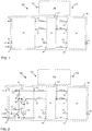
- FIG. 1 schematically illustrates a solid state switch, SSS, driver circuit 100 according to a first embodiment of the present invention.
- the SSS driver circuit 100 is configured for controlling a solid state switch, SSS, 150, interconnected between a stack node 201 and a supply node 202.
- the stack node 201 is connected to a battery cell stack that provides an output voltage of the battery cell stack, e.g., 48 V, to the stack node 201.
- the supply node 202 is configured to be connected to one or more loads or a load circuit for supplying power to the one or more loads.
- the SSS 150 is configured to selectively connect or disconnect the stack node 201 and the supply node 202. Particularly, the SSS 150 shall enable to disconnect the battery cell stack from any load in an abnormal operation condition.
- the SSS 150 is operated as a high side switch between the stack and the supply node 202.
- the SSS driver circuit 100 of the first embodiment is configured to output a control signal to the SSS 150, particularly to a gate node 151 of the SSS 150.
- the control signal is output to the gate node via an output node of the SSS driver circuit 100 that corresponds to the gate node 151.
- the control signal output by the SSS driver circuit 100 to the SSS 150 is for selectively setting the SSS 150 conductive or non-conductive and is generated as explained in the following.
- the SSS driver circuit 100 as shown in Figure 1 comprises a voltage generation circuit 10, a shut off circuit 30 and a switch controller 50. These sub-circuits of the SSS driver circuit 100 realize different functionalities in the SSS driver circuit and are characterized by their respective inputs and outputs as follows.
- the voltage generation circuit, VGC, 10 comprises a first input node that receives a supply voltage, V SUP , which is supplied indirectly by the battery cell stack, preferably by a system basis chip of a battery system comprising the battery cells.
- the VGC 10 further comprises a second input node 12 that receives an output voltage of the battery cell stack, in the following referred to as GND Driver .
- the VGC 10 further comprises a first ground node 13 for receiving a ground voltage, GND.
- the ground voltage GND preferably is a common ground of the SSS driver circuit 100, the stack and the battery system.
- the VGC 10 is configured for generating a drive voltage VCC Driver using the supply voltage V SUP and the output voltage GND Driver .
- the drive voltage is higher than V SUP as well as higher than GND Driver .
- GND Driver is higher than V SUP , preferably V SUP is about 20 V and GND Driver is about 48 V.
- the drive voltage VCC Driver is suitable for setting the SSS 150 conductive when it is applied to the gate node 151 of the SSS 150.
- the drive voltage VCC Driver is generated in dependence of a first control signal.
- the first control signal is applied to the VGC 10 via a first control node 14 and preferably is a pulse-width-modulating, PWM, signal.
- the duty cycle of the PWM signal received via the first control node 14 preferably controls the amplitude of the drive voltage VCC Driver .
- the VGC 10 operates as a DCDC converter the conversion ratio of which is controlled via the first control signal.
- the drive voltage VCC Driver is output to a first output node 15 of the VGC 10.
- the drive voltage VCC Driver is output continuously to the first output node 15.
- the function of the VGC 10 is to generate a voltage that is high enough to set conductive a high side SSS 150 interconnected between a battery stack and a load from a voltage provided by that battery stack, i.e., performs a voltage up conversion operation.
- the SSS driver circuit 100 of the invention further comprises a switch off circuit, SOC, 30 that comprises a third input node that also receives the output voltage GND Driver .
- the SOC 30 further comprises a second ground node that also receives the ground voltage, GND.
- the SOC 30 comprises a second control node 32 that receives a second control signal OFF1 and further comprises a third control node 34 that receives a third control signal, OFF2.
- the second control signal and the third control signal are preferably binary signals, i.e., take one of two values, e.g., of a high value "1" and a low value "0". Therein, these values can be represented by specific voltages or specific currents.
- the SOC 30 is configured for outputting the output voltage GND Driver to a second output node 35 in dependence of the second and third control signals.
- the SOC 30 is configured to output a voltage for setting non-conductive the high side SSS 150 in dependence of two signals, i.e., OFF1 and OFF2.
- the SOC 30 is configured to output the GND Driver if at least one of the two control signals OFF1 and OFF2 takes a specific value, e.g., a high value "1". Otherwise, the SOC 30 does not output the GND Driver to the second output node 35 and hence the second output node 35 is floating.
- the output's dependency of the second control signal OFF1 and the third control signal OFF2 provides redundancy in setting the SSS 150 non-conductive and thus increases the operational safety of the SSS 150.
- the SSS driver circuit 100 further comprises a switch controller 50, which is another subcircuit of the SSS driver circuit 100.
- the switch controller 50 is connected to the first output node 15 of the VGC 10 from which it receives the drive voltage VCC Driver generated in dependence of the first control signal.
- the switch controller 50 is further connected to the second output node 35 of the shut off circuit 30 from which it receives the output voltage GND Driver in dependence of the second and third control signal.
- the switch controller 50 further comprises a third ground node 53 that also receives the ground voltage GND.
- the switch controller 50 further comprises a fourth control node 54 that receives a fourth control signal ON1.
- the fourth control signal is a binary signal, i.e., takes one of two values, e.g., either a high value "1" or a low value "0". Therein, these values can be represented by specific voltages or specific currents.
- the switch controller 50 is configured to forward one of the received voltages, VCC Driver , and GND Driver , to a gate node 151 of the solid state switch 150 via an output node of the switch controller 50 and in in dependence of the fourth control signal, ON1. In other words, if the fourth control signal takes a first value the switch controller 50 outputs VCC Driver and when the fourth control signal takes a second value the switch controller 50 outputs GND Driver or a floating voltage to the gate node 151.
- the SSS driver circuit 100 of the invention allows the operation of a SSS 150 using solely voltages supplied within the battery system as well as a minimal set of control signals, while maintaining high functional safety during operation. Particularly, solely if ON1 is applied with a first value to switch controller 50, the VCC Driver voltage is output to the gate node 151 and the SSS 150 is set conductive. Otherwise, the voltage present at the second output node 35 is directly forwarded to the gate node 151. Further, if at least one of OFF1 and OFF2 is applied with a certain value to SOC 30, the GND Driver voltage is applied to the second output node 35 and, if ON1 takes a second value, to the gate node 151 and SSS 150 is set non-conductive.
- the SSS driver circuit 100 provides a cost-effective solution for controlling the SSS 150 without the need for e.g., a transformer for generating VCC Driver , and with improved redundancy in setting non-conductive the SSS 150 based on the two signals OFF1, OFF2.
- Figure 2 schematically illustrates a solid state switch driver circuit 100 according to a second embodiment.
- the basic configuration of the embodiment as illustrated in Figure 2 is identical to the embodiment as shown in Figure 1 .
- a repeated description is omitted and the same reference signs are used for the same components.
- the embodiment of Figure 2 is distinguished by the use of specific components as described in the following.
- VGC 10 of the SSS driver circuit 100 of Figure 2 comprises a first capacitor C1 16 with a first capacitor node 161 and a second capacitor node 162.
- the first capacitor node 161 is connected to the first input node 11 via a first diode 17, particularly the first capacitor node 161 is connected to the cathode of the first diode 17 and the cathode of the first diode 17 is connected to the first input node 11.
- the first capacitor node 161 is also connected to the first output node 15, i.e., is interconnected between the first output node 15 and the cathode of the first diode 17.
- the second capacitor node 162 is connected to ground node 13 via a first switch 18 and is connected to the second input node 12 via a second switch 19.
- the first switch 18 is a first MOSFET T 1 (n-channel) with a source node connected to the first ground node 13 and a drain node connected to the second capacitor node 162.
- the gate of the first MOSFET T 1 is connected to the first control node 14, i.e., receives the first control signal, PWM.
- PWM takes a high value, e.g., "1" or VDD
- the ground voltage GND is applied to the second capacitor node 162 via the first switch 18.
- the first capacitor 16 is charged via the first diode 17 with V SUP provided by the first input node 11 and hence a voltage drop between GND and V SUP occurs over C1.
- second switch 19 is a second MOSFET T 2 (p-channel) with a source node connected to the second input node 12 and a drain node connected to second capacitor node 162.
- a gate node of second MOSFET T 2 is connected to first ground node 13 via another n-channel MOSFET T 10 , a source node of which is connected to first ground node 13, a drain node of which is connected to the gate node of the second MOSFET T 2 and a gate node of which is connected to the first control node 14 via an inverter 23.
- the MOSFET T 10 is set conductive and connects the first ground node 13 with the gate node of second MOSFET T 2 and thus sets second MOSFET T 2 conductive. Then, the second input node 12 is connected to the second capacitor node 162 which is thus set to the potential GND Driver . Due to the voltage drop over the charged first capacitor 16 C1 thus a voltage equal to the sum of V SUP and GND Driver applies to the first capacitor node 161.
- the VGC 10 operates as a DCDC converter with flying cap capacitor C1.
- n-channel MOSFET could be used for second switch T 2 , the gate of MOSFET T2 being then connected to the first control node 14 via the first converter 23.
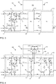
- Figure 3 schematically illustrates a solid state switch driver circuit 100 according to a third embodiment.
- the basic configuration of the embodiment as illustrated in Figure 3 is identical to the embodiment as shown in Figures 1, 2 .
- a repeated description is omitted and the same reference signs are used for the same components.
- the embodiment of Figure 3 is distinguished by the use of specific components as described in the following.
- the VGC 10 further comprises a Zener diode 20 that is interconnected in parallel to the first capacitor 16 in between the first output node 15 and the second input node 12.
- the cathode of the Zener diode 20 is connected to a node that is interconnected between the first output node 15 and the first capacitor node 161 of the first capacitor 16.
- the anode of the Zener diode 20 is connected to a node that is interconnected between the second switch 19 and the second input node 12.
- the Zener diode 20 functions as a protection diode that is configured for ensuring that the drive voltage VCC Driver is limited to a certain value. Hence, the third switch T 3 is protected.
- the VGC 10 of the third embodiment further comprises a second capacitor 21 that is interconnected in parallel to the first capacitor 16 in between the first output node 15 and the second input node 12.
- a first capacitor node of the second capacitor 21 is interconnected between the first output node 15 and the node connected to the cathode of the Zener diode 20.
- a second capacitor node of the second capacitor 21 is interconnected between the second input node 12 and the node connected to the anode of the Zener diode 20.
- the second capacitor 21 is charged with the voltage that applies to the first capacitor node 161 of the first capacitor 16 over the second diode 22.
- the second capacitor 21 when the second switch is set conductive, the second capacitor 21 is charged with the drive voltage VCC Driver , i.e., the first capacitor node of the second capacitor 21 is charged to the drive voltage VCC Driver .
- the second capacitor 21 stores energy for setting the first output node 15 to VCC Driver even if the voltage V SUP or the first control signals PWM is not longer supplied to the VGC 10.
- the charged second capacitor 21 is configured to provide energy for setting SSS 150 conductive for a predetermined time period, preferably for a time period that allows fulfilling ASIL B requirements with respect to availability of the SSS 150, e.g., for a time of 35 s to 1 min.
- Figure 4 schematically illustrates a solid state switch driver circuit 100 according to a fourth embodiment.
- the basic configuration of the embodiment as illustrated in Figure 4 is identical to the embodiment as shown in Figures 1 to 3 . Insofar, a repeated description is omitted and the same reference signs are used for the same components. However, the embodiment of Figure 4 is distinguished by the use of specific components as described in the following.
- the solid state switch, SSS, 150 is specified to comprise at least one set of anti-serially interconnected FETs, wherein each set comprising at least one first FET, TA, 203 and at least one second FET, TB, 204.
- the gate contacts of the FETs 203, 204 are electrically interconnected and the source contacts of the FETs 203, 204 are electrically interconnected.
- the drain contact(s) of the at least one first FET 203 is/are electrically connected to the stack node 201 and the drain contact(s) of the at least one second FET 204 is/are electrically connected to the supply node 202.
- both FETs 203, 204 can be controlled at once by applying a gate voltage to the gates of the FETs 203, 204 via the gate node 151.
- the SSS 150 comprises a first flyback diode 205 connected in parallel with the first FET 203 and a second flyback diode 206 connected in parallel with the second FET 204, these diodes protecting the FETs 203, 204.
- the SOC 30 comprises a fifth switch 36 that is a fifth p-channel MOSFET T 5 with a drain node connected to the third input node 31, i.e., receiving GND Driver , and a drain node connected to the second output node 35.
- a gate node of MOSFET T 5 is connected to the second ground node 33 via a sixth switch 38 that is a sixth n-channel MOSFET T 6 .
- the source node of MOSFET T 6 is connected to the second ground node 33
- the drain node of MOSFET T 6 is connected to the gate node of MOSFET T 5
- a gate node of MOSFET T 6 is connected to the second control node 32.
- MOSFET T 6 is set conductive and applies ground voltage GND to the gate node of MOSFET T 5 .
- the gate channel of MOSFET T 5 is set conductive and the cell stack's output voltage GND Driver is applied to the second output node and to the gate node 151 of the SSS 150, thus setting the FETs 203 ,204 non-conductive, hence disconnecting stack node 201 from supply node 202.
- the SOC 30 comprises a seventh switch 37 that is a seventh p-channel MOSFET T 7 with a drain node connected to the third input node 31, i.e., receiving GND Driver , and a drain node connected to the second output node 35.
- a gate node of MOSFET T 7 is connected to the second ground node 33 via an eighth switch 39 that is a eighth n-channel MOSFET T 8 .
- the source node of MOSFET T 8 is connected to the second ground node 33
- the drain node of MOSFET T 8 is connected to the gate node of MOSFET T 7
- a gate node of MOSFET T 8 is connected to the third control node 34.
- MOSFET T 8 is set conductive and applies ground voltage GND to the gate node of MOSFET T 7 .
- the gate channel of MOSFET T 7 is set conductive and the cell stack's output voltage GND Driver is applied to the second output node and to the gate node 151 of the SSS 150, thus setting the FETs 203, 204 non-conductive, hence disconnecting stack node 201 from supply node 202.
- the switch controller 50 comprises a third switch 51 that is a third p-channel MOSFET T 3 a source node of which is connected to the first output node 15 and a drain node of which is connected to the gate node 151, i.e., to a node interconnected between the gate node 151 and the second output node 35. That is, a voltage applied to the drain node of MOSFET T 3 is applied to gate node 151 insofar it is higher than the voltage that applies to the second output node 35.
- the gate node of the MOSFET T 3 is connected to the third ground node 53 via a fourth switch 52 that is a fourth n-channel MOSFET T 4 .
- the source node of MOSFET T 4 is connected to the third ground node 53, the drain node of the MOSFET T 4 is connected to the gate node of MOSFET T 3 and the gate node of MOSFET T 4 is connected to the fourth control node 54, i.e., receives fourth control signal ON1. That is, if the fourth control signal ON1 takes a high value, e.g., "1" or VDD, MOSFET T 4 is set conductive and applies ground voltage GND to the gate node of MOSFET T 3 . Hence, the gate channel of MOSFET T 3 is set conductive and the voltage at the first output node 15 is applied to the gate node 151 of SSS 150 setting FETs 203, 204 conductive.
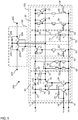
- Figure 5 schematically illustrates a solid state switch driver circuit 100 according to a fifth embodiment.
- the basic configuration of the embodiment as illustrated in Figure 5 is identical to the embodiment as shown in Figures 1 to 4 . Insofar, a repeated description is omitted and the same reference signs are used for the same components. However, the embodiment of Figure 5 is distinguished by the use of specific components as described in the following.
- the SSS driver circuit 100 further comprises a first diagnostic circuit 60 that is configured to output a first diagnostic signal, DIAG 1 , indicating a potential at the second input node 12 and to output a second diagnostic signal, DIAG2, indicating a potential at the first output node 15.
- the first diagnostic circuit 60 comprises a first voltage divider 61 with a first divider node connected to the second input node 12 and a second diver node connected to the first ground node 13. An output node of the first voltage divider 61 then provides the first diagnostic signal DIAG1.
- the first diagnostic circuit 60 comprises a second voltage divider 62 with a first divider node connected to the first output node 15 and a second diver node also connected to first ground node 13. An output node of the second voltage divider 62 then provides the second diagnostic signal DIAG2. The first diagnostic circuit 60 thus provides diagnostic signals that are indicative of the voltage drop over the second capacitor 21 as described above.
- the first diagnostic circuit 60 allows detecting malfunctions in the battery system 200, as the first diagnostic circuit 60 receives the same voltage, GND Driver , as applied to the input of the SSS.
- the first diagnostic circuit further allows testing of the fifth switch T 5 and the seventh switch T 7 .
- the drive voltage VCC Driver is generated with a voltage that is lower than V TH of the power MOSFETs 203, 204.
- the functionality of T 5 and T 7 is tested individually by setting OFF1 and OFF2 to high signal individually and detecting the voltage with the first voltage divider 61, while third switch T 3 is set conductive via ON1.
- VCC Driver is controlled to be less than V TH of FETs 203, 204 the SSS 150 is not closed.
- third switch T 3 can be tested by detecting DIAG 1 and comparing it to the signal DIAG2 representative of the voltage at first output node 15.
- the SSS driver circuit 100 further comprises a second diagnostic circuit 70 that is configured to output a third diagnostic signal, DIAG 3 , which is indicating a potential at the second output node 35.
- the second diagnostic circuit 70 is configured to output a third diagnostic signal, DIAG 3 , indicating a potential at the drain node of the third switch MOSFET T 3 or more precisely the voltage at a node interconnected between the drain node of MOSFET T 3 and the second output node 35.
- the second diagnostic circuit 70 comprises a third voltage divider 71 with a first divider node connected in between the second output node 35 and the drain node of the third switch MOSFET T 3 and a second divider node connected to ground, GND.
- the second diagnostic circuit 70 allows for testing the functionality of the switches T 3 also while operating the voltage generation circuit 10 with a PWM signal that leads to an output voltage at the first output node that is less than the V TH of the power FETs 203, 204.
- the second diagnostic circuit may be further used for testing the switching off capability of the fifth and seventh switches T 5 , T 7 .
Landscapes
- Engineering & Computer Science (AREA)
- Power Engineering (AREA)
- Life Sciences & Earth Sciences (AREA)
- Sustainable Development (AREA)
- Sustainable Energy (AREA)
- Transportation (AREA)
- Mechanical Engineering (AREA)
- Electronic Switches (AREA)
- Charge And Discharge Circuits For Batteries Or The Like (AREA)
Priority Applications (3)
| Application Number | Priority Date | Filing Date | Title |
|---|---|---|---|
| EP19162233.1A EP3708403B1 (fr) | 2019-03-12 | 2019-03-12 | Circuit de commande de commutateur à semiconducteurs pour un système de batterie |
| KR1020200021658A KR102468333B1 (ko) | 2019-03-12 | 2020-02-21 | 솔리드 스테이트 스위치 드라이버 회로 및 이를 포함하는 전지시스템 |
| US16/815,752 US11444337B2 (en) | 2019-03-12 | 2020-03-11 | Solid state switch driver circuit for a battery system |
Applications Claiming Priority (1)
| Application Number | Priority Date | Filing Date | Title |
|---|---|---|---|
| EP19162233.1A EP3708403B1 (fr) | 2019-03-12 | 2019-03-12 | Circuit de commande de commutateur à semiconducteurs pour un système de batterie |
Publications (2)
| Publication Number | Publication Date |
|---|---|
| EP3708403A1 true EP3708403A1 (fr) | 2020-09-16 |
| EP3708403B1 EP3708403B1 (fr) | 2021-01-20 |
Family
ID=65801879
Family Applications (1)
| Application Number | Title | Priority Date | Filing Date |
|---|---|---|---|
| EP19162233.1A Active EP3708403B1 (fr) | 2019-03-12 | 2019-03-12 | Circuit de commande de commutateur à semiconducteurs pour un système de batterie |
Country Status (2)
| Country | Link |
|---|---|
| EP (1) | EP3708403B1 (fr) |
| KR (1) | KR102468333B1 (fr) |
Citations (4)
| Publication number | Priority date | Publication date | Assignee | Title |
|---|---|---|---|---|
| EP1531535A2 (fr) * | 2003-11-14 | 2005-05-18 | Sony Corporation | Bloc-batterie, appareil de traitement de protection de batterie, et procédé de commande du démarrage de l'appareil de traitement de protection de batterie |
| US20110051303A1 (en) * | 2008-03-13 | 2011-03-03 | Paolo Migliavacca | Method for providing over-voltage protection and circuit therefor |
| US20180152035A1 (en) * | 2016-10-03 | 2018-05-31 | O2Micro Inc. | Charge/discharge switch control circuits for batteries |
| EP3352322A1 (fr) * | 2017-01-24 | 2018-07-25 | Samsung SDI Co., Ltd | Unité de commande pour système de batterie |
-
2019
- 2019-03-12 EP EP19162233.1A patent/EP3708403B1/fr active Active
-
2020
- 2020-02-21 KR KR1020200021658A patent/KR102468333B1/ko active IP Right Grant
Patent Citations (4)
| Publication number | Priority date | Publication date | Assignee | Title |
|---|---|---|---|---|
| EP1531535A2 (fr) * | 2003-11-14 | 2005-05-18 | Sony Corporation | Bloc-batterie, appareil de traitement de protection de batterie, et procédé de commande du démarrage de l'appareil de traitement de protection de batterie |
| US20110051303A1 (en) * | 2008-03-13 | 2011-03-03 | Paolo Migliavacca | Method for providing over-voltage protection and circuit therefor |
| US20180152035A1 (en) * | 2016-10-03 | 2018-05-31 | O2Micro Inc. | Charge/discharge switch control circuits for batteries |
| EP3352322A1 (fr) * | 2017-01-24 | 2018-07-25 | Samsung SDI Co., Ltd | Unité de commande pour système de batterie |
Non-Patent Citations (2)
| Title |
|---|
| MAXIM INTEGRATED: "DC-DC Conversion Without Inductors", MAXIM DESIGN SUPPORT, TECHNICAL DOCUMENTS, TUTORIALS, POWER-SUPPLY CIRCUITS, APP 725, 22 July 2009 (2009-07-22), pages 1 - 8, XP055623085, Retrieved from the Internet <URL:https://pdfserv.maximintegrated.com/en/an/AN725.pdf> [retrieved on 20190917] * |
| TOSHIBA: "MOSFET Gate Drive Circuit Application Note", 26 July 2018 (2018-07-26), pages 1 - 22, XP055622261, Retrieved from the Internet <URL:https://toshiba.semicon-storage.com> [retrieved on 20190913] * |
Also Published As
| Publication number | Publication date |
|---|---|
| KR102468333B1 (ko) | 2022-11-16 |
| KR20200110177A (ko) | 2020-09-23 |
| EP3708403B1 (fr) | 2021-01-20 |
Similar Documents
| Publication | Publication Date | Title |
|---|---|---|
| EP3576241B1 (fr) | Système de batterie | |
| US20200317085A1 (en) | Control electronics for a battery system, method for power supplying control electronics for a battery system, battery system and vehicle | |
| EP3620321B1 (fr) | Système d'alimentation électrique | |
| US11063460B2 (en) | Battery system | |
| EP3722137A1 (fr) | Électronique de commande pour un système de batterie, procédé de fourniture d'alimentation à l'électronique de commande pour un système de batterie, système de batterie et véhicule | |
| US11084397B2 (en) | Power supply system for vehicle with multiple operating voltages | |
| EP3675319A1 (fr) | Bloc-batterie et dispositif électronique le comprenant | |
| US20220093984A1 (en) | Battery protection apparatus and battery system including the same | |
| US11329564B2 (en) | Control system for a battery system | |
| EP3863141A1 (fr) | Système de batterie | |
| KR102555492B1 (ko) | 전지 시스템용 제어 시스템, 전지 시스템 및 이를 포함하는 차량 | |
| EP3680955B1 (fr) | Système de batterie | |
| US11801753B2 (en) | Battery system and vehicle including the battery system | |
| EP3708403B1 (fr) | Circuit de commande de commutateur à semiconducteurs pour un système de batterie | |
| US20210249872A1 (en) | Battery system | |
| US11444337B2 (en) | Solid state switch driver circuit for a battery system | |
| EP4060785A1 (fr) | Système de batterie et véhicule comprenant le système de batterie | |
| US11476690B2 (en) | Power supply system | |
| EP3890059A1 (fr) | Système de batterie de véhicule électrique comprenant une horloge en temps réel | |
| EP3337002B1 (fr) | Système de batterie et unité de commande pour un système de batterie | |
| US20220407427A1 (en) | Bidirectional power supply system for powering a battery management system of an electric vehicle | |
| EP4108496A1 (fr) | Système d'alimentation bidirectionnelle pour alimenter un système de gestion de batterie d'un véhicule électrique | |
| US20230170538A1 (en) | Battery system and method for operating the same | |
| US11884182B2 (en) | Electric-vehicle battery system including a real time clock | |
| EP4186746A1 (fr) | Système de batterie et son procédé de fonctionnement |
Legal Events
| Date | Code | Title | Description |
|---|---|---|---|
| PUAI | Public reference made under article 153(3) epc to a published international application that has entered the european phase |
Free format text: ORIGINAL CODE: 0009012 |
|
| STAA | Information on the status of an ep patent application or granted ep patent |
Free format text: STATUS: REQUEST FOR EXAMINATION WAS MADE |
|
| 17P | Request for examination filed |
Effective date: 20200324 |
|
| AK | Designated contracting states |
Kind code of ref document: A1 Designated state(s): AL AT BE BG CH CY CZ DE DK EE ES FI FR GB GR HR HU IE IS IT LI LT LU LV MC MK MT NL NO PL PT RO RS SE SI SK SM TR |
|
| AX | Request for extension of the european patent |
Extension state: BA ME |
|
| GRAP | Despatch of communication of intention to grant a patent |
Free format text: ORIGINAL CODE: EPIDOSNIGR1 |
|
| STAA | Information on the status of an ep patent application or granted ep patent |
Free format text: STATUS: GRANT OF PATENT IS INTENDED |
|
| INTG | Intention to grant announced |
Effective date: 20201029 |
|
| GRAS | Grant fee paid |
Free format text: ORIGINAL CODE: EPIDOSNIGR3 |
|
| GRAA | (expected) grant |
Free format text: ORIGINAL CODE: 0009210 |
|
| STAA | Information on the status of an ep patent application or granted ep patent |
Free format text: STATUS: THE PATENT HAS BEEN GRANTED |
|
| AK | Designated contracting states |
Kind code of ref document: B1 Designated state(s): AL AT BE BG CH CY CZ DE DK EE ES FI FR GB GR HR HU IE IS IT LI LT LU LV MC MK MT NL NO PL PT RO RS SE SI SK SM TR |
|
| REG | Reference to a national code |
Ref country code: GB Ref legal event code: FG4D |
|
| REG | Reference to a national code |
Ref country code: CH Ref legal event code: EP |
|
| REG | Reference to a national code |
Ref country code: DE Ref legal event code: R096 Ref document number: 602019002221 Country of ref document: DE |
|
| REG | Reference to a national code |
Ref country code: AT Ref legal event code: REF Ref document number: 1356104 Country of ref document: AT Kind code of ref document: T Effective date: 20210215 |
|
| REG | Reference to a national code |
Ref country code: IE Ref legal event code: FG4D |
|
| REG | Reference to a national code |
Ref country code: NL Ref legal event code: MP Effective date: 20210120 |
|
| REG | Reference to a national code |
Ref country code: LT Ref legal event code: MG9D |
|
| REG | Reference to a national code |
Ref country code: AT Ref legal event code: MK05 Ref document number: 1356104 Country of ref document: AT Kind code of ref document: T Effective date: 20210120 |
|
| PG25 | Lapsed in a contracting state [announced via postgrant information from national office to epo] |
Ref country code: PT Free format text: LAPSE BECAUSE OF FAILURE TO SUBMIT A TRANSLATION OF THE DESCRIPTION OR TO PAY THE FEE WITHIN THE PRESCRIBED TIME-LIMIT Effective date: 20210520 Ref country code: NO Free format text: LAPSE BECAUSE OF FAILURE TO SUBMIT A TRANSLATION OF THE DESCRIPTION OR TO PAY THE FEE WITHIN THE PRESCRIBED TIME-LIMIT Effective date: 20210420 Ref country code: LT Free format text: LAPSE BECAUSE OF FAILURE TO SUBMIT A TRANSLATION OF THE DESCRIPTION OR TO PAY THE FEE WITHIN THE PRESCRIBED TIME-LIMIT Effective date: 20210120 Ref country code: BG Free format text: LAPSE BECAUSE OF FAILURE TO SUBMIT A TRANSLATION OF THE DESCRIPTION OR TO PAY THE FEE WITHIN THE PRESCRIBED TIME-LIMIT Effective date: 20210420 Ref country code: FI Free format text: LAPSE BECAUSE OF FAILURE TO SUBMIT A TRANSLATION OF THE DESCRIPTION OR TO PAY THE FEE WITHIN THE PRESCRIBED TIME-LIMIT Effective date: 20210120 Ref country code: HR Free format text: LAPSE BECAUSE OF FAILURE TO SUBMIT A TRANSLATION OF THE DESCRIPTION OR TO PAY THE FEE WITHIN THE PRESCRIBED TIME-LIMIT Effective date: 20210120 Ref country code: GR Free format text: LAPSE BECAUSE OF FAILURE TO SUBMIT A TRANSLATION OF THE DESCRIPTION OR TO PAY THE FEE WITHIN THE PRESCRIBED TIME-LIMIT Effective date: 20210421 |
|
| PG25 | Lapsed in a contracting state [announced via postgrant information from national office to epo] |
Ref country code: PL Free format text: LAPSE BECAUSE OF FAILURE TO SUBMIT A TRANSLATION OF THE DESCRIPTION OR TO PAY THE FEE WITHIN THE PRESCRIBED TIME-LIMIT Effective date: 20210120 Ref country code: LV Free format text: LAPSE BECAUSE OF FAILURE TO SUBMIT A TRANSLATION OF THE DESCRIPTION OR TO PAY THE FEE WITHIN THE PRESCRIBED TIME-LIMIT Effective date: 20210120 Ref country code: RS Free format text: LAPSE BECAUSE OF FAILURE TO SUBMIT A TRANSLATION OF THE DESCRIPTION OR TO PAY THE FEE WITHIN THE PRESCRIBED TIME-LIMIT Effective date: 20210120 Ref country code: AT Free format text: LAPSE BECAUSE OF FAILURE TO SUBMIT A TRANSLATION OF THE DESCRIPTION OR TO PAY THE FEE WITHIN THE PRESCRIBED TIME-LIMIT Effective date: 20210120 Ref country code: SE Free format text: LAPSE BECAUSE OF FAILURE TO SUBMIT A TRANSLATION OF THE DESCRIPTION OR TO PAY THE FEE WITHIN THE PRESCRIBED TIME-LIMIT Effective date: 20210120 |
|
| PG25 | Lapsed in a contracting state [announced via postgrant information from national office to epo] |
Ref country code: IS Free format text: LAPSE BECAUSE OF FAILURE TO SUBMIT A TRANSLATION OF THE DESCRIPTION OR TO PAY THE FEE WITHIN THE PRESCRIBED TIME-LIMIT Effective date: 20210520 |
|
| REG | Reference to a national code |
Ref country code: DE Ref legal event code: R097 Ref document number: 602019002221 Country of ref document: DE |
|
| PG25 | Lapsed in a contracting state [announced via postgrant information from national office to epo] |
Ref country code: SM Free format text: LAPSE BECAUSE OF FAILURE TO SUBMIT A TRANSLATION OF THE DESCRIPTION OR TO PAY THE FEE WITHIN THE PRESCRIBED TIME-LIMIT Effective date: 20210120 Ref country code: CZ Free format text: LAPSE BECAUSE OF FAILURE TO SUBMIT A TRANSLATION OF THE DESCRIPTION OR TO PAY THE FEE WITHIN THE PRESCRIBED TIME-LIMIT Effective date: 20210120 Ref country code: EE Free format text: LAPSE BECAUSE OF FAILURE TO SUBMIT A TRANSLATION OF THE DESCRIPTION OR TO PAY THE FEE WITHIN THE PRESCRIBED TIME-LIMIT Effective date: 20210120 Ref country code: MC Free format text: LAPSE BECAUSE OF FAILURE TO SUBMIT A TRANSLATION OF THE DESCRIPTION OR TO PAY THE FEE WITHIN THE PRESCRIBED TIME-LIMIT Effective date: 20210120 |
|
| PLBE | No opposition filed within time limit |
Free format text: ORIGINAL CODE: 0009261 |
|
| STAA | Information on the status of an ep patent application or granted ep patent |
Free format text: STATUS: NO OPPOSITION FILED WITHIN TIME LIMIT |
|
| PG25 | Lapsed in a contracting state [announced via postgrant information from national office to epo] |
Ref country code: DK Free format text: LAPSE BECAUSE OF FAILURE TO SUBMIT A TRANSLATION OF THE DESCRIPTION OR TO PAY THE FEE WITHIN THE PRESCRIBED TIME-LIMIT Effective date: 20210120 Ref country code: SK Free format text: LAPSE BECAUSE OF FAILURE TO SUBMIT A TRANSLATION OF THE DESCRIPTION OR TO PAY THE FEE WITHIN THE PRESCRIBED TIME-LIMIT Effective date: 20210120 Ref country code: RO Free format text: LAPSE BECAUSE OF FAILURE TO SUBMIT A TRANSLATION OF THE DESCRIPTION OR TO PAY THE FEE WITHIN THE PRESCRIBED TIME-LIMIT Effective date: 20210120 |
|
| REG | Reference to a national code |
Ref country code: BE Ref legal event code: MM Effective date: 20210331 |
|
| 26N | No opposition filed |
Effective date: 20211021 |
|
| PG25 | Lapsed in a contracting state [announced via postgrant information from national office to epo] |
Ref country code: IE Free format text: LAPSE BECAUSE OF NON-PAYMENT OF DUE FEES Effective date: 20210312 Ref country code: LU Free format text: LAPSE BECAUSE OF NON-PAYMENT OF DUE FEES Effective date: 20210312 Ref country code: AL Free format text: LAPSE BECAUSE OF FAILURE TO SUBMIT A TRANSLATION OF THE DESCRIPTION OR TO PAY THE FEE WITHIN THE PRESCRIBED TIME-LIMIT Effective date: 20210120 Ref country code: ES Free format text: LAPSE BECAUSE OF FAILURE TO SUBMIT A TRANSLATION OF THE DESCRIPTION OR TO PAY THE FEE WITHIN THE PRESCRIBED TIME-LIMIT Effective date: 20210120 |
|
| PG25 | Lapsed in a contracting state [announced via postgrant information from national office to epo] |
Ref country code: IT Free format text: LAPSE BECAUSE OF FAILURE TO SUBMIT A TRANSLATION OF THE DESCRIPTION OR TO PAY THE FEE WITHIN THE PRESCRIBED TIME-LIMIT Effective date: 20210120 |
|
| PG25 | Lapsed in a contracting state [announced via postgrant information from national office to epo] |
Ref country code: IS Free format text: LAPSE BECAUSE OF FAILURE TO SUBMIT A TRANSLATION OF THE DESCRIPTION OR TO PAY THE FEE WITHIN THE PRESCRIBED TIME-LIMIT Effective date: 20210520 |
|
| PG25 | Lapsed in a contracting state [announced via postgrant information from national office to epo] |
Ref country code: BE Free format text: LAPSE BECAUSE OF NON-PAYMENT OF DUE FEES Effective date: 20210331 |
|
| REG | Reference to a national code |
Ref country code: CH Ref legal event code: PL |
|
| PG25 | Lapsed in a contracting state [announced via postgrant information from national office to epo] |
Ref country code: LI Free format text: LAPSE BECAUSE OF NON-PAYMENT OF DUE FEES Effective date: 20220331 Ref country code: CH Free format text: LAPSE BECAUSE OF NON-PAYMENT OF DUE FEES Effective date: 20220331 |
|
| PGFP | Annual fee paid to national office [announced via postgrant information from national office to epo] |
Ref country code: FR Payment date: 20230309 Year of fee payment: 5 |
|
| PG25 | Lapsed in a contracting state [announced via postgrant information from national office to epo] |
Ref country code: NL Free format text: LAPSE BECAUSE OF NON-PAYMENT OF DUE FEES Effective date: 20210120 Ref country code: CY Free format text: LAPSE BECAUSE OF FAILURE TO SUBMIT A TRANSLATION OF THE DESCRIPTION OR TO PAY THE FEE WITHIN THE PRESCRIBED TIME-LIMIT Effective date: 20210120 |
|
| P01 | Opt-out of the competence of the unified patent court (upc) registered |
Effective date: 20230528 |
|
| PG25 | Lapsed in a contracting state [announced via postgrant information from national office to epo] |
Ref country code: SI Free format text: LAPSE BECAUSE OF FAILURE TO SUBMIT A TRANSLATION OF THE DESCRIPTION OR TO PAY THE FEE WITHIN THE PRESCRIBED TIME-LIMIT Effective date: 20210120 Ref country code: HU Free format text: LAPSE BECAUSE OF FAILURE TO SUBMIT A TRANSLATION OF THE DESCRIPTION OR TO PAY THE FEE WITHIN THE PRESCRIBED TIME-LIMIT; INVALID AB INITIO Effective date: 20190312 |
|
| PG25 | Lapsed in a contracting state [announced via postgrant information from national office to epo] |
Ref country code: MK Free format text: LAPSE BECAUSE OF FAILURE TO SUBMIT A TRANSLATION OF THE DESCRIPTION OR TO PAY THE FEE WITHIN THE PRESCRIBED TIME-LIMIT Effective date: 20210120 |
|
| PGFP | Annual fee paid to national office [announced via postgrant information from national office to epo] |
Ref country code: DE Payment date: 20240227 Year of fee payment: 6 Ref country code: GB Payment date: 20240229 Year of fee payment: 6 |