EP3708358A1 - Laminated body, antireflection structure, and camera module mounting device - Google Patents
Laminated body, antireflection structure, and camera module mounting device Download PDFInfo
- Publication number
- EP3708358A1 EP3708358A1 EP18877179.4A EP18877179A EP3708358A1 EP 3708358 A1 EP3708358 A1 EP 3708358A1 EP 18877179 A EP18877179 A EP 18877179A EP 3708358 A1 EP3708358 A1 EP 3708358A1
- Authority
- EP
- European Patent Office
- Prior art keywords
- reflection
- light shielding
- light
- reflection structure
- shielding film
- Prior art date
- Legal status (The legal status is an assumption and is not a legal conclusion. Google has not performed a legal analysis and makes no representation as to the accuracy of the status listed.)
- Granted
Links
Images



Classifications
-
- G—PHYSICS
- G02—OPTICS
- G02B—OPTICAL ELEMENTS, SYSTEMS OR APPARATUS
- G02B1/00—Optical elements characterised by the material of which they are made; Optical coatings for optical elements
- G02B1/10—Optical coatings produced by application to, or surface treatment of, optical elements
- G02B1/11—Anti-reflection coatings
- G02B1/118—Anti-reflection coatings having sub-optical wavelength surface structures designed to provide an enhanced transmittance, e.g. moth-eye structures
-
- B—PERFORMING OPERATIONS; TRANSPORTING
- B32—LAYERED PRODUCTS
- B32B—LAYERED PRODUCTS, i.e. PRODUCTS BUILT-UP OF STRATA OF FLAT OR NON-FLAT, e.g. CELLULAR OR HONEYCOMB, FORM
- B32B7/00—Layered products characterised by the relation between layers; Layered products characterised by the relative orientation of features between layers, or by the relative values of a measurable parameter between layers, i.e. products comprising layers having different physical, chemical or physicochemical properties; Layered products characterised by the interconnection of layers
- B32B7/02—Physical, chemical or physicochemical properties
- B32B7/023—Optical properties
-
- G—PHYSICS
- G02—OPTICS
- G02F—OPTICAL DEVICES OR ARRANGEMENTS FOR THE CONTROL OF LIGHT BY MODIFICATION OF THE OPTICAL PROPERTIES OF THE MEDIA OF THE ELEMENTS INVOLVED THEREIN; NON-LINEAR OPTICS; FREQUENCY-CHANGING OF LIGHT; OPTICAL LOGIC ELEMENTS; OPTICAL ANALOGUE/DIGITAL CONVERTERS
- G02F1/00—Devices or arrangements for the control of the intensity, colour, phase, polarisation or direction of light arriving from an independent light source, e.g. switching, gating or modulating; Non-linear optics
- G02F1/01—Devices or arrangements for the control of the intensity, colour, phase, polarisation or direction of light arriving from an independent light source, e.g. switching, gating or modulating; Non-linear optics for the control of the intensity, phase, polarisation or colour
- G02F1/13—Devices or arrangements for the control of the intensity, colour, phase, polarisation or direction of light arriving from an independent light source, e.g. switching, gating or modulating; Non-linear optics for the control of the intensity, phase, polarisation or colour based on liquid crystals, e.g. single liquid crystal display cells
- G02F1/133—Constructional arrangements; Operation of liquid crystal cells; Circuit arrangements
- G02F1/1333—Constructional arrangements; Manufacturing methods
- G02F1/1335—Structural association of cells with optical devices, e.g. polarisers or reflectors
- G02F1/133502—Antiglare, refractive index matching layers
-
- G—PHYSICS
- G02—OPTICS
- G02F—OPTICAL DEVICES OR ARRANGEMENTS FOR THE CONTROL OF LIGHT BY MODIFICATION OF THE OPTICAL PROPERTIES OF THE MEDIA OF THE ELEMENTS INVOLVED THEREIN; NON-LINEAR OPTICS; FREQUENCY-CHANGING OF LIGHT; OPTICAL LOGIC ELEMENTS; OPTICAL ANALOGUE/DIGITAL CONVERTERS
- G02F1/00—Devices or arrangements for the control of the intensity, colour, phase, polarisation or direction of light arriving from an independent light source, e.g. switching, gating or modulating; Non-linear optics
- G02F1/01—Devices or arrangements for the control of the intensity, colour, phase, polarisation or direction of light arriving from an independent light source, e.g. switching, gating or modulating; Non-linear optics for the control of the intensity, phase, polarisation or colour
- G02F1/13—Devices or arrangements for the control of the intensity, colour, phase, polarisation or direction of light arriving from an independent light source, e.g. switching, gating or modulating; Non-linear optics for the control of the intensity, phase, polarisation or colour based on liquid crystals, e.g. single liquid crystal display cells
- G02F1/133—Constructional arrangements; Operation of liquid crystal cells; Circuit arrangements
- G02F1/1333—Constructional arrangements; Manufacturing methods
- G02F1/1335—Structural association of cells with optical devices, e.g. polarisers or reflectors
- G02F1/133509—Filters, e.g. light shielding masks
- G02F1/133512—Light shielding layers, e.g. black matrix
Definitions
- the present disclosure relates to a laminate, an anti-reflection structure and a camera module mounting apparatus that can be thinned, are excellent in anti-reflection performance and can keep reflection chromaticity neutral.
- a display device such as a liquid crystal display or an optical device such as a camera is often subjected to anti-reflection treatment such as formation of an anti-reflection film on an incident surface of light on a base material such as a display plate or a lens in order to avoid deterioration of visibility and image quality (generation of color unevenness, ghost, or the like) due to reflection of light from the outside.
- anti-reflection treatment such as formation of an anti-reflection film on an incident surface of light on a base material such as a display plate or a lens in order to avoid deterioration of visibility and image quality (generation of color unevenness, ghost, or the like) due to reflection of light from the outside.
- Patent Literature (PTL) 1 discloses a solid-state image sensor configured to construct an image through photoelectric conversion of light incident on a semiconductor substrate, in which a fine uneven structure is formed on a light incident surface of a semiconductor substrate and an anti-reflection film having a predetermined thickness is formed on the fine uneven structure so as to reduce generation of reflection of light on the light incident surface.
- thinning e. g. 15 ⁇ m or less
- a total thickness of an outermost layer and a middle layer should be equal to or greater than 25 ⁇ m, and there was a room for improvement in terms of thinning.
- the inventors of the present disclosure have found that a high anti-reflection performance can be realized while reducing the thickness by forming an anti-reflection structure having a fine uneven structure on the surface thereof through an adhesion layer and by setting an uneven period of the fine uneven structure to be equal to or less than the wavelength of visible light, and in addition, a reflection chromaticity can be kept neutral between the surface subjected to the anti-reflection treatment technique and its surrounding surface by setting a difference in color between the reflected light by the light shielding film and the reflected light by the anti-reflection structure to be small (specifically, equal to or less than 1.5).
- a laminate and an anti-reflection structure that can be thinned are excellent in anti-reflection performance and can keep reflection chromaticity neutral can be provided. Further, according to the present disclosure, a camera module mounting apparatus in which thinning is achieved by using the laminate and a captured image with reduced color unevenness can be provided.
- FIGS. 1 to 3 may be schematically represented by a scale or a shape different from the actual ones for convenience of explanation.
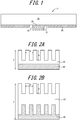
- the laminate according to the present disclosure is a laminate 1 including a display plate 10, a light shielding film 20 provided on the display plate 10 and an anti-reflection structure 30 having a fine uneven structure on a surface thereof, as illustrated in FIG. 1 .
- a part of the light shielding film 20 has a non-light shielding portion 21 without the light shielding film 20, the anti-reflection structure 30 is formed in the non-light shielding portion 21 through an adhesion layer 40, the fine uneven structure 30 has an uneven period P equal to or less than the wavelength of visible light (see FIG. 2 ), and a color difference ( ⁇ E) between the reflected light by the light shielding film and the reflected light by the anti-reflection structure expressed in a formula shown below is equal to or less than 1.5.
- ⁇ E a 1 ⁇ a 2 2 + b 1 ⁇ b 2 2 (where a 1 and b 1 represent a* and b* values of the light reflected by the light shielding film in the CIE1976 (L *a*b*) color system, and a 2 and b 2 represent a* and b* values of the light reflected by the anti-reflection structure in the CIE1976 (L *a*b*) color system.)
- a high anti-reflection performance can be realized while thinning is achieved by forming an anti-reflection structure 30 having a fine uneven structure on the surface thereof through the adhesion layer 40 and setting an uneven period P of the fine uneven structure 30 to be equal to or less than the wavelength of the visible light.
- a color difference ⁇ E between the reflected light by the light shielding film 20 and the reflected light by the anti-reflection structure 30 is small such as equal to or less than 1.5, the reflection chromaticity can be kept neutral between the surface treated with the anti-reflection treatment technique (the surface of the anti-reflection structure 30 in FIG. 1 ) and its surrounding surface (the surface of the light shielding film 20 in FIG. 1 ).
- the laminate 1 includes the display plate 10.
- the display plate 10 is a member serving as a substrate or a support plate of the laminate 1 according to the present disclosure.
- Materials of the display plate 10 are not particularly limited, and may be appropriately selected according to the purpose of use of the laminate.
- the material of the display plate may be glass, polymethyl methacrylate (PMMA) or the above described materials whose surface is coated with an organic material (polyimide, etc.), and the like.
- the display plate may preferably be transparent so as to transmit light, since the display plate is used as a liquid crystal display, a touch panel and the like.
- transparent herein means a transmittance of the light of the wavelength belonging to the visible light band (about 360 nm to 830 nm) is high, and for example, means that a transmittance of the light is equal to or greater than 70%.
- the shape of the display plate is not particularly limited except that it has a plate shape, and can be appropriately selected according to the purpose of use of the laminate.
- the surface on which the light shielding film and the anti-reflection structure are laminated (in FIG. 1 , under the display plate 10) may be a flat face, for example, so that they can be easily formed.
- the laminate 1 according to the present disclosure further includes the light shielding film 20 on the display plate 10 as illustrated in FIG. 1 .
- the light shielding film 20 enhances the light-shielding effect, and blocks the light from reaching a solid-state image sensor even if a thinned display plate 10 transmits the light (in particular the light with a wavelength of equal to or greater than 800 nm).
- a material constituting the light shielding film is not particularly limited, and a known light shielding film can be appropriately used depending on the use.
- a composition for a light shielding film in which a binder resin contains light-shielding particles, a filler, other additives and the like can be used.
- binder resin examples include, for example, (meth) acrylic resin, urethane resin, polyvinyl alcohol, polyvinyl butyral, polyvinyl formal, polyamide, polyester, and the like, and include (meth) acrylic resin, urethane resin, and the like.
- These resins may have a carboxylic acid group, a sulfonate group, a phonic acid group, a phonic acid group, a sulfonamide group, and the like, as an acid group,
- the light-shielding particles include, for example, inorganic pigment such as carbon black, titanium black, tungsten compound, zinc oxide, lead white, lithopon, titanium oxide, chromium oxide, iron oxide, precipitated barium sulfate and barite powder, red lead, red iron oxide, yellow lead, zinc yellow (zinc yellow type 1 and zinc yellow type 2), ultramarine blue, procyanide blue (potassium ferrocyanide), zircon gray, praseodymium yellow, chrome titanium yellow, chrome green, peacock, victorial green, iron blue (unrelated to Prussian blue), vanadium zirconium blue, chrome tin pink, manganese pink, salmon pink and the like.
- inorganic pigment such as carbon black, titanium black, tungsten compound, zinc oxide, lead white, lithopon, titanium oxide, chromium oxide, iron oxide, precipitated barium sulfate and barite powder
- red lead red iron oxide, yellow lead, zinc yellow (zinc yellow type 1 and zinc yellow type
- black pigment a metal oxide, a metal nitrogen, a mixture thereof, or the like containing one or more metal elements selected from the group consisting of Co, Cr, Cu, Mn, Ru, Fe, Ni, Sn, Ti, and Ag can be used.
- the light-shielding particles may also include light-shielding dyes such as, for example, cyanine dyes, phthalocyanine dyes, naphthalocyanine dyes, immonium dyes, aminium dyes, quinolium dyes, pyrylium dyes, or metal complex dyes such as Ni complex dyes.
- light-shielding dyes such as, for example, cyanine dyes, phthalocyanine dyes, naphthalocyanine dyes, immonium dyes, aminium dyes, quinolium dyes, pyrylium dyes, or metal complex dyes such as Ni complex dyes.
- the content of the light-shielding particles in the light-shielding film composition is not particularly limited, but is preferably from 30 to 70 mass%, more preferably from 40 to 60 mass%, and still more preferably from 45 to 55 mass%, based on the total solid content.
- composition for a light shielding film may contain fillers and other additives as necessary.
- the filler is not particularly limited as long as it increases the reflectance, and for example, an organic filler, an inorganic filler, or an inorganic-organic composite filler can be used.
- organic filler examples include, for example, synthetic resin particles, natural polymer particles, and the like, and preferably resin particles such as acrylic resin, polyethylene, polypropylene, polyethylene oxide, polypropylene oxide, polyethyleneimine, polystyrene, polyurethane, polyurea, polyester, polyamide, polyimide, carboxymethylcellulose, gelatin, starch, chitin, chitosan, and the like.
- resin particles such as acrylic resin, polyethylene, polypropylene, polyethylene oxide, polypropylene oxide, polyethyleneimine, polystyrene, polyurethane, polyurea, polyester, polyamide, polyimide, carboxymethylcellulose, gelatin, starch, chitin, chitosan, and the like.
- the inorganic filler examples include metals and metal compounds such as silica, mica compound, glass, zinc oxide, alumina, zircon oxide, tin oxide, potassium titanate, strontium titanate, aluminum borate, magnesium oxide, magnesium borate, aluminum hydroxide, magnesium hydroxide, calcium hydroxide, titanium hydroxide, basic magnesium sulfate, calcium carbonate, magnesium carbonate, calcium sulfate, magnesium sulfate, calcium silicate, magnesium silicate, calcium phosphate, silicon nitride, titanium nitride, aluminum nitride, silicon carbide, titanium carbide, zinc sulfide, and at least two or more of these compounds.
- metals and metal compounds such as silica, mica compound, glass, zinc oxide, alumina, zircon oxide, tin oxide, potassium titanate, strontium titanate, aluminum borate, magnesium oxide, magnesium borate, aluminum hydroxide, magnesium hydroxide, calcium hydroxide, titanium hydroxide, basic magnesium sulfate
- additives examples include known additives such as a polymerizable compound, a polymerization initiator, a dispersant, a sensitizer, a crosslinking agent effect accelerator, and a surfactant.
- the average thickness of the light shielding film 20 is not particularly limited, it is preferably equal to or less than 30 ⁇ m, and more preferably equal to or less than 10 ⁇ m in terms of thinning of the laminate 1. Moreover, the thickness of the light shielding film 20 is preferably equal to or greater than 3 ⁇ m in terms of maintaining a high light-shielding effect.
- the average thickness of the light shielding film 20 is obtained by taking the average of the portion where the light shielding film 20 is formed, excepting the thickness of the non-light shielding portion 21 described later.
- it can be obtained by taking the average of thicknesses of any five portions of the light shielding film 20, for example.
- a part of the light shielding film 20 is constituted of a non-light shielding portion 21 where no light shielding film 20 is formed. This is because, when the anti-reflection structure 30 described later is provided in the non-light shielding portion 21, thinning of the laminate 1 is promoted and an anti-reflection action can be sufficiently exhibited as well.
- non-light shielding portion 21 is a portion of the light shielding film 20 where no light shielding film is formed.
- the above described non-light shielding portion 21 may be a through hole as illustrated in FIG. 1 or a partially transparent material may be filled therein.
- the size of the non-light shielding portion 21 is not particularly limited, and may be changed according to the size of the anti-reflection structure 30.
- the portion where the anti-reflection structure 30 is not formed be as small as possible so as to reliably block the light reaching the solid-state image sensor.
- the anti-reflection structure 30 be formed in a range of preferably 50% and more preferably 100% of the area of the non-light shielding portion 21 (i.e., the opening area of the light shielding film 20).
- the method of forming the light shielding film 20 is not particularly limited, and a known forming method can be appropriately used depending on the thickness of the light shielding film 20, the manufacturing facility, and the like.
- the light-shielding film 20 can be formed by applying the above described light-shielding film composition to the display plate 10 by spin coating, spray coating, slit coating, inkjet coating, rotation coating, flow casting coating, roll coating, screen printing, or the like, followed by curing treatment such as light irradiation treatment or heat treatment.
- the laminate 1 according to the present disclosure has, in the non-light shielding portion 21 thereof, the anti-reflection structure 30 having a fine uneven structure formed on the surface thereof.
- the anti-reflection structure 30 can enhance the anti-reflection performance of the laminate 1 by the fine uneven structure formed on the surface thereof.
- FIG. 2A illustrates an embodiment of the anti-reflection structure 30 and the adhesion layer 40.
- Each projection and each recess of the fine uneven structure of the anti-reflection structure 30 may be periodically disposed (e.g., staggered lattice shape, rectangular lattice shape), as illustrated in FIG. 2A , and may also be disposed randomly.
- the shape of the projection and the recess is not particularly limited, and may be artillery, conical, columnar, or needle shaped and the like. It is to be noted that the shape of the recess means a shape formed by the inner wall of the recess.
- the fine uneven structure of the anti-reflection structure 30 has an uneven period (uneven pitch) P that is equal to or less than the wavelength of visible light (e.g. 830 nm or less).
- the upper limit of the uneven period P is preferably equal to or less than 350 nm and more preferably equal to or less than 280 nm
- the lower limit of the uneven period P is preferably equal to or greater than 100 nm, and more preferably equal to or greater than 150 nm.
- the uneven period P of the fine uneven structure is set to not more than the visible light wavelength, in other words, the fine uneven structure is formed in what is called a "moth-eye structure," and as a result an excellent anti-reflection performance can be realized.
- the uneven period P of the uneven structure is an arithmetic mean value of the distances between adjacent protrusions and adjacent recesses.
- the uneven period P can be observed, for example, using a scanning electron microscope (SEM) or a cross-section transmission electron microscope (cross-section TEM) and the like.
- the method by which the arithmetic mean value between adjacent protrusions and adjacent recesses is calculated may, for example, be a method in which a plurality of combinations of adjacent protrusions and a plurality of combinations of adjacent recesses are selected, the distances between the protrusions and the distances between the recesses in these combinations are measured, and the measured values are averaged.
- the average uneven height (the depth of recess) H of the fine uneven structure may preferably be equal to or greater than 190 nm so as to keep the reflection chromaticity neutral in more reliable manner.
- the average uneven height P of the fine uneven structure may preferably be equal to or less than 320 nm in terms of thinning of the laminate.
- the uneven height H of the fine uneven structure is a distance from the bottom of the recess to the vertex of the protrusion, as illustrated in FIG. 2A , and the average uneven height can be obtained by measuring some uneven heights H (e. g., five portions) and averaging them.
- the thickness of the support portion under the fine uneven structure of the anti-reflection structure 30 where the fine uneven structure is not formed is not particularly limited, and may be about from 500 nm to 9000 nm.
- the fine uneven structure of the anti-reflection structure 30 is needed to be provided on the surface on the side that does not come in contact with at least the adhesion layer 40, as illustrated in FIG. 2A .
- the fine uneven structure can be provided on both sides, as illustrated in FIG. 2B .
- the material of the anti-reflection structure 30 is not particularly limited.
- the material include, for example, a resin composition that is cured by a curing reaction, such as an active energy ray curable resin composition (photocurable resin composition, electron beam curable resin composition), thermosetting resin composition, or the like, and for example, a resin composition containing a polymerizable compound and a polymerization initiator.
- polymerizable compound for example, (i) an esterified product obtained by reacting (meth) acrylic acid or a derivative thereof in a ratio of equal to or greater than 2 mol to 1 mol of polyhydric alcohol, (ii) an esterified product obtained by a polyhydric alcohol, a polyvalent carboxylic acid or an anhydride thereof, an (meth)acrylic acid or a derivative thereof, and the like can be used.
- Examples of the above described (i) include 1,4-butanediol di(meth)acrylate, 1,6-hexanediol di(meth)acrylate, 1,9-nonanediol di(meth)acrylate, trimethylol propantri(meth)acrylate, trimethylol ethantri(meth)acrylate, pentaerythritol tri(meth)acrylate, pentaerythritol tetra(meth)acrylate, tetrahydrofuryl acrylate, glycerin tri(meth)acrylate, dipentaerythritol penta(meth)acrylate, dipentaerythritol hexa(meth)acrylate, tripentaerythritol hexa(meth)acrylate, tripentaerythritol hepta(meth)acrylate, acryloimonofoline, urethane acrylate, and the
- Examples of the above described (ii) include polyhydric alcohols such as trimethylolethane, trimethylolpropane, glycerin, and pentaerythritol; polycarboxylic acids or anhydrides thereof selected from malonic acid, succinic acid, adipic acid, glutaric acid, sebacic acid, fumaric acid, itaconic acid, maleic anhydride, and the like; and esterified products obtained by reacting (meth)acrylic acid or derivatives thereof.
- polyhydric alcohols such as trimethylolethane, trimethylolpropane, glycerin, and pentaerythritol
- polycarboxylic acids or anhydrides thereof selected from malonic acid, succinic acid, adipic acid, glutaric acid, sebacic acid, fumaric acid, itaconic acid, maleic anhydride, and the like
- esterified products obtained by reacting (meth)acrylic acid or derivatives thereof include polyhydric
- These polymerizable compounds may be used alone or two or more types may be used in combination.
- photopolymerization initiators include, for example: carbonyl compounds such as benzoin, benzoin methyl ether, benzoin ethyl ether, benzoin isopropyl ether, benzoin isobutyl ether, benzyl, benzophenone, p-methoxybenzophenone, 2,2-diethoxyacetophenone, ⁇ , ⁇ -dimethoxy- ⁇ -phenylacetophenone, methylphen ylglyoxylate, ethylphenylglyoxylate, 4,4'-bis(dimethylamino)benzophenone, 1-hydroxycyclohexyl phenyl ketone, 2-hydroxy-2-methyl-1-phenyl-propan-1-one, and the like; sulfur compounds such as tetramethylthiuram monosulphide, tetramethylthiuram disulfide, and the like; 2,4,6-trimethylbenzoyl diphenyl-
- examples of the electron beam polymerization initiator include: thioxanthones such as benzophenone, 4,4-bis(di ethylamino)benzophenone, 2,4,6-trimethylbenzophenone, methylorthobenzoylbenzoate, 4-phenylbenzophenone, t-butylanthraquinone, 2-ethylanthraquinone, 2,4-diethylthioxanthone, isopropylthioxanthone, 2,4-dichlorothioxanthone, and the like; acetophenones such as diethoxyacetophenone, 2-hydroxy-2-methyl-1-phenylpro pane-1-one, benzyl dimethyl ketal, 1-hydroxycyclohexyl-phenyl ketone, 2-methyl-2 -morpholino(4-thiomethylphenyl)propane-1-one, 2-benzyl-2-dimethylamino
- thermal polymerization initiators include: organic peroxides such as methyl ethyl ketone peroxide, benzoyl peroxide, dicumyl peroxide, t-butyl hydroperoxide, cumene hydroperoxide, t-butyl peroxyoctoate, t-butyl peroxybenzoate, lauroyl peroxide, and the like; azo-based compounds such as azobisisobutyronitrile; and redox polymerization initiators obtained by combining amines such as N,N-dimeth ylaniline, N,N-dimethyl-p-toluidine with the above described organic peroxides.
- organic peroxides such as methyl ethyl ketone peroxide, benzoyl peroxide, dicumyl peroxide, t-butyl hydroperoxide, cumene hydroperoxide, t-butyl peroxyoctoate, t-butyl peroxybenz
- photopolymerization initiators electron beam polymerization initiators, and thermal polymerization initiators may be used alone or in combination as desired.
- the amount of polymerization initiator is preferably 0.01 to 10 parts by mass with respect to 100 parts by mass of polymerizable compound. In such a range, the curing proceeds sufficiently, the molecular weight of the cured product becomes appropriate, and sufficient strength is obtained, and there is no problem that the cured product is colored due to the residue of the polymerization initiator or the like.
- the resin composition may contain a non-reactive polymer or an active energy ray sol-gel reactive component, and may contain various additives such as a thickener, a leveling agent, an ultraviolet absorber, a light stabilizer, a thermal stabilizer, a solvent, an inorganic filler, and the like, as necessary.
- the method of producing the anti-reflection structure 30 is not particularly limited.
- an antireflection structure 30 having a fine uneven structure on the surface thereof can be obtained by performing a clamping/crimping step, a curing step, and a peeling step.
- a resin composition for anti-reflection structure is clamped and crimped between a holding film having a fine uneven structure on the surface thereof and a holding film having a flat surface.
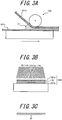
- a holding film having a fine uneven structure on the surface thereof (a first holding film 201a) and a holding film having a flat surface (a second holding film 201b) are provided. Subsequently, as illustrated in FIG. 3A , a resin composition for anti-reflection structure 151 is clamped between the first holding film 201a and the second holding film 201b.
- the holding film 201a having a fine uneven structure on the surface thereof can be produced by forming a fine uneven layer having a predetermined recess-protrusion pattern on a base substrate made of a transparent and hard to break material (e.g., polyethylene terephthalate, triacetyl cellulose, etc.).
- the clamped body is crimped in the clamping direction by a crimping apparatus 160 such as a roll laminator, and the like.
- a crimping apparatus 160 such as a roll laminator, and the like.
- the thickness of the anti-reflection structure 30 that is obtained finally can be adjusted by adjusting the pressure during crimping.
- the clamped resin composition for anti-reflection structure 151 is cured by irradiating with active energy rays such as UV light to form the anti-reflection structure 30 having a fine uneven structure on both sides theteof.
- the clamped resin composition for anti-reflection structure 151 is irradiated with active energy rays to cure the resin composition for anti-reflection structure 151.
- the resin composition for anti-reflection structure 151 is cured, a holding film laminate 250 including the anti-reflection structure 30 having a fine uneven structure on the surface thereof is obtained.
- the curing step may be performed at the same timing as that of the clamping/crimping step.
- the holding films 201a and 201b are peeled from the holding film laminate 250 to obtain the anti-reflection structure 30.
- the obtained anti-reflection structure 30 is subjected to a treatment such as cleaning or the like as necessary.
- the method of producing the anti-reflection structure 30 is not limited to the above described method of performing a clamping/crimping step, a curing step and a peeling step ( FIGS. 3A to 3C ), and the anti-reflection structure 30 can be produced by forming a fine uneven structure by sputtering and the like after the resin composition for anti-reflection structure is cured, for example.
- the laminate 1 according to the present disclosure further includes an adhesion layer 40 configured to bond the anti-reflection structure 30 to the non-light shielding portion 21, as illustrated in FIG. 1 .
- the adhesion layer 40 is made of an adhesive in order to bond the anti-reflection structure 30 to the non-light shielding portion 21. However, it is necessary to use a material that does not deteriorate the anti-reflection performance of the anti-reflection structure 30.
- the adhesive layer 40 is preferably made of an ultraviolet curable adhesive to obtain a high bonding property.
- the ultraviolet curable resin include an ultraviolet curable acrylic resin, an ultraviolet curable epoxy resin, and the like.
- the method of forming the adhesion layer 40 is not particularly limited.
- the adhesion layer 40 is a layer made of an ultraviolet curable adhesive
- the adhesion layer 40 can be formed by irradiating ultraviolet rays to the non-light shielding portion 21 in a state where the ultraviolet curable adhesive is crimped with the anti-reflection structure 30.
- the adhesion layer 40 is thinned in a range in which a high bonding property can be maintained in terms of thinning the laminate 1.
- a total thickness T of the anti-reflection structure 30 and the adhesion layer 40 may preferably be equal to or less than 30 ⁇ m, and more preferably be equal to or less than 10 ⁇ m.
- a color difference ( ⁇ E) between the reflected light by the light shielding film 20 and the reflected light by the anti-reflection structure 30 expressed in the a formula shown below is equal to or less than 1.5.
- ⁇ E a 1 ⁇ a 2 2 + b 1 ⁇ b 2 2
- a 1 and b 1 represent a* and b* values of the light reflected by the light shielding film 20 in the CIE1976 (L *a*b*) color system
- a 2 and b 2 represent a* and b* values of the light reflected by the anti-reflection structure 30 in the CIE1976 (L *a*b*) color system.
- the CIE1976 (L*a*b*) color system is one of the uniform color spaces defined by CIE in 1976, and a color space using three-dimensional orthogonal coordinates of the lightness index L and the chromaticity indices a* and b* is called an L*a*b* color space, and is a color system using this color space.
- the ⁇ E needs to be equal to or less than 1.5, in terms of making the reflection chromaticity of the surface of the anti-reflection structure 30 and its surrounding surface more neutral, it is preferably equal to or less than 1.0, and more preferably equal to or less than 0.7.
- the a* value and b* values of the light reflected by the light shielding film 20 in the CIE1976 (L *a*b*) color system and a* value and b* values of the light reflected by the anti-reflection structure 30 in the CIE1976 (L *a*b*) color system can be obtained by using commercially available measuring devices.
- a* value and b* value in the CIE1976 (L*a*b*) color system and the color difference ⁇ E can be adjusted by changing the material, the shape and the thickness of the light shielding film 20, the material of the anti-reflection structure 30, the uneven period P of the uneven structure, the uneven height H of the uneven structure, and the like.
- the difference ( ⁇ Y) between the luminous reflectance (Y value) of the light shielding film 20 and the luminous reflectance (Y value) of the anti-reflection structure 30 is preferably equal to or less than 0.5. This is because, since the brightness on the chromaticity diagram can be set substantially the same condition, the reflection chromaticity between the surface of the anti-reflection structure 30 and its surrounding surface can be maintained more neutral.
- the luminous reflectance (Y value) is a reflectance obtained in consideration that the brightness perceived by eyes is changed by the visibility sensitivity, and is (X, Y, Z) when representing the color of the positive reflected light in the CIE1931 XYZ color space, or (x, y, Y) when representing the color of the positive reflected light in the CIE xyY color space.
- the visual reflectance can be measured with a commercially available spectrometer (e.g., V650, etc., from JASCO Corporation).
- the luminous reflectance and the difference in reflectance of each of the light shielding film and the anti-reflection structure 30 can be adjusted by changing the density or the uneven height of the fine uneven structure, for example.
- the camera module mounting apparatus 300 includes a laminate 1 according to the present disclosure and a camera module 310 provided at a position facing the anti-reflection structure 30 in the laminate, as illustrated in FIG. 4 .
- a still image or a moving image can be photographed by an image sensor of the camera module through the laminate of the present disclosure, thus reflection of light is suppressed, and occurrence of color unevenness and the like can be suppressed in a captured image obtained.
- a model of the laminate 1 including a display plate 10, a light shielding film 20 provided on the display plate 10 and an anti-reflection structure 30 having a fine uneven structure on the surface thereof was produced as illustrated in FIG. 1 .
- the chromaticity of reflected light irradiation angle : 5° was calculated.
- the display plate 10 was a glass substrate, and the light shielding film 20 contained carbon black, and was formed by applying a spray paint containing butyl acetate, ethyl acetate, nitrocellulose, diisobutyl ketone, isopropyl alcohol, isobutanol, and the like to the surface of the glass substrate.
- Table 1 shows the structure of the antireflection structure, the total thickness ( ⁇ m) of the anti-reflection structure and the adhesive layer, and the calculation results of the a* value and the b* value (a 2 and b 2 ) of the light reflected by the anti-reflection structure in the CIE1976 (L*a*b*) color system and the color difference ⁇ E between the reflected light by the light shielding film and the reflected light by the anti-reflection structure.
- Example 1-1 a laminate was produced under the same conditions as in Example 1-1 except that, as an anti-reflection technique, an anti-reflection film (Dry-AR direct forming) was formed by alternately laminating four layers in total of NbOx and SiO 2 instead of the anti-reflection structure 30 having a fine uneven structure.
- an anti-reflection film Dry-AR direct forming
- Table 1 shows the antireflection structure, the total thickness ( ⁇ m) of the anti-reflection structure and the adhesive layer, and the calculation results of the a* value and the b* value of the light reflected by the anti-reflection structure in the CIE1976 (L*a*b*) color system and the color difference ⁇ E between the reflected light by the light shielding film and the reflected light by the anti-reflection structure.
- an anti-reflection film Wet-AR direct coating
- Table 1 shows the antireflection structure, the total thickness ( ⁇ m) of the anti-reflection structure and the adhesive layer, and the calculation results of the a* value and the b* value of the light reflected by the anti-reflection structure in the CIE1976 (L*a*b*) color system and the color difference ⁇ E between the reflected light by the light shielding film and the reflected light by the anti-reflection structure.
- an antireflection film Wet-AR film lamination
- Table 1 shows the antireflection structure, the total thickness ( ⁇ m) of the anti-reflection structure and the adhesive layer, and the calculation results of the a* value and the b* value of the light reflected by the anti-reflection structure in the CIE1976 (L*a*b*) color system and the color difference ⁇ E between the reflected light by the light shielding film and the reflected light by the anti-reflection structure.
- Example 1-2 to 1-7 and Comparative Examples 1-4 to 1-7 a laminate was produced under the same conditions as in Example 1-1 except that the uneven height was changed (for specific height of the uneven height, see Table 2) with respect to the fine uneven structure of the anti-reflection structure 30.
- Table 3 shows an uneven height (nm) of the anti-reflection structure, the a* value and the b* value of the light reflected by the anti-reflection structure in the CIE1976 (L*a*b*), and the color difference ⁇ E between the reflected light by the light shielding film and the reflected light by the anti-reflection structure (Dry-AR direct forming).
- a laminate 1 including a display plate 10, a light shielding film 20 provided on the display plate 10 and an anti-reflection structure 30 having a fine uneven structure on the surface thereof was actually produced.
- the chromaticity of each reflected light irradiation angle : 5 ° was measured.
- the display plate 10 was a glass substrate, and the light shielding film 20 contained carbon black, and was formed by applying a spray paint containing butyl acetate, ethyl acetate, nitrocellulose, diisobutyl ketone, isopropyl alcohol, isobutanol, and the like to the surface of the glass substrate.
- the anti-reflection structure 30 was formed of "UVX-6366" (ultraviolet curable resins consisting of 1,6-hexanediol diacrylate, tetrahydrofuryl acrylate, and 2,4,6-trimethylbenzoyl diphenyl phosphine oxide) from TOAGOSEI CO., LTD., and had an uneven period of the fine uneven structure of 150 to 250 nm, an uneven height of 220 nm, a thickness of the base portion without the fine uneven structure of 1000nm. Moreover, ultraviolet curing resin is used for the adhesion layer 40, and a thickness thereof was 3780 nm. A total thickness of the anti-reflection structure 30 and the adhesion layer 40 is 5000 nm (5 ⁇ .tm).
- Table 2 shows a structure of the antireflection structure, the total thickness ( ⁇ m) of the anti-reflection structure and the adhesive layer, and the calculation results of the a* value and the b* value of the light reflected by the anti-reflection structure in the CIE1976 (L*a*b*) and the color difference ⁇ E between the reflected light by the light shielding film and the reflected light by the anti-reflection structure.
- Table 1 shows that the ⁇ E of Example 1-1 is the smallest, and the reflection chromaticity is kept neutral.
- the optical spectrum was obtained by using an ultraviolet visible near-infrared spectrophotometer "V-650" from JASCO Corporation, and on the basis of that, the a* value and the b* value of the light reflected by the anti-reflection structure in the CIE1976 (L*a*b*) and the color difference ⁇ E between the reflected light by the light shielding film and the reflected light by the anti-reflection structure were calculated. The measuring results are shown in Table 2.
- Table 2 shows that ⁇ E is kept small, and the reflection chromaticity is kept neutral with respect to Example 2, as with Example 1-1.
- the spectral wavelength and reflectance (5°) of each sample of Examples 1-2 to 1-7 and Comparative Examples 1-4 to 1-7 were calculated using the calculation software "TFCalc," and the relationship between the wavelength and the reflectance is shown in FIGS. 7A and 7B . Furthermore, the a* value and the b* value of the light reflected by the anti-reflection structure in the CIE1976 (L*a*b*), and the color difference ⁇ E between the reflected light by the light shielding film and the reflected light by the anti-reflection structure were also calculated, and the calculation results are shown in FIG. 3 .
- FIG. 7 and Table 3 show that, when the uneven height of the uneven structure is equal to or greater than 190 nm, ⁇ E can be kept within the range of the present disclosure (the determination result is "pass"). Thus an excellent anti-reflection performance could be realized, and reflection chromaticity could be kept neutral.
- a laminate and an anti-reflection structure that can be thinned, are excellent in anti-reflection performance and can keep reflection chromaticity neutral can be provided. Further, according to the present disclosure, a camera module mounting apparatus can be provided, in which thinning is achieved by using the laminate and a captured image with reduced color unevenness can be obtained.
Landscapes
- Physics & Mathematics (AREA)
- General Physics & Mathematics (AREA)
- Optics & Photonics (AREA)
- Nonlinear Science (AREA)
- Mathematical Physics (AREA)
- Chemical & Material Sciences (AREA)
- Crystallography & Structural Chemistry (AREA)
- Laminated Bodies (AREA)
- Surface Treatment Of Optical Elements (AREA)
- Liquid Crystal (AREA)
- Transforming Light Signals Into Electric Signals (AREA)
Abstract
Description
- The present disclosure relates to a laminate, an anti-reflection structure and a camera module mounting apparatus that can be thinned, are excellent in anti-reflection performance and can keep reflection chromaticity neutral.
- A display device such as a liquid crystal display or an optical device such as a camera is often subjected to anti-reflection treatment such as formation of an anti-reflection film on an incident surface of light on a base material such as a display plate or a lens in order to avoid deterioration of visibility and image quality (generation of color unevenness, ghost, or the like) due to reflection of light from the outside.
- Here, as one of existing anti-reflection treatments, a technique of forming a fine uneven structure on a light incident surface so as to reduce reflectance is known.
- For example, Patent Literature (PTL) 1 discloses a solid-state image sensor configured to construct an image through photoelectric conversion of light incident on a semiconductor substrate, in which a fine uneven structure is formed on a light incident surface of a semiconductor substrate and an anti-reflection film having a predetermined thickness is formed on the fine uneven structure so as to reduce generation of reflection of light on the light incident surface.
- PLT 1:
JP2015054402A - When the above described anti-reflection film treatment technique is considered to be applied to a field of small electronic devices and the like, thinning (e. g. 15 µm or less) is required. However, in the technique disclosed in PTL 1, in order to form a fine uneven structure without causing any problems, a total thickness of an outermost layer and a middle layer should be equal to or greater than 25 µm, and there was a room for improvement in terms of thinning.
- Moreover, when a multilayer-film anti-reflection structure as disclosed in PTL 1 is used, coloration may occur in the reflected light, and a difference in reflection color may occur as compared with the peripheral portion, thus the sense of unity of color is impaired.
- Thus, in consideration of application to a cover film provided on a front surface of a sensor or to a cover film provided on a front surface of a camera module sensor, development of an anti-reflection treatment technique that causes no difference in the reflection color between the surface to which the anti-reflection treatment technique is applied and its surrounding surface (hereinafter referred to as "the reflection chromaticity is kept neutral").
- The present disclosure has been made in light of the circumstances set forth above, and an object thereof is to provide a laminate and an anti-reflection structure that are thinned, are excellent in anti-reflection performance and can keep reflection chromaticity neutral. Another object of the present disclosure is to provide a camera module mounting apparatus capable of being thinned by using the above described laminate and obtaining a captured image with reduced color unevenness.
- As a result of intensive research to solve the above described problem, the inventors of the present disclosure have found that a high anti-reflection performance can be realized while reducing the thickness by forming an anti-reflection structure having a fine uneven structure on the surface thereof through an adhesion layer and by setting an uneven period of the fine uneven structure to be equal to or less than the wavelength of visible light, and in addition, a reflection chromaticity can be kept neutral between the surface subjected to the anti-reflection treatment technique and its surrounding surface by setting a difference in color between the reflected light by the light shielding film and the reflected light by the anti-reflection structure to be small (specifically, equal to or less than 1.5).
- The present disclosure is made on the basis of the above described findings, and the scope thereof is as follows:
- (1) A laminate including a display plate, a light shielding film provided on the display plate and an anti-reflection structure having a fine uneven structure on a surface thereof, wherein
a part of the light shielding film has a non-light shielding portion without a light shielding film;
the anti-reflection structure is formed in the non-light shielding portion through an adhesion layer, and the fine uneven structure has an uneven period equal to or less than the wavelength of visible light; and
a color difference (ΔE) between reflected light by the light shielding film and reflected light by the anti-reflection structure expressed in the formula shown below is equal to or less than 1.5.
The above described configuration allows for thinning, an excellent anti-reflection performance and a reflection chromaticity kept in neutral. - (2) The laminate according to (1), wherein a total thickness of the anti-reflection structure and the adhesion layer is equal to or less than 30 µm.
- (3) The laminate according to (1) or (2), wherein the adhesion layer is a layer made of an ultraviolet curing adhesive.
- (4) The laminate according to any one of claims (1) to (3), wherein an average uneven height of the fine uneven structure is equal to or greater than 190 nm.
- (5) The laminate according to any one of (1) to (4), wherein a difference (ΔY) between a luminous reflectance of the light shielding film (hereinafter referred to also as "Y value") and a luminous reflectance of the anti-reflection structure (Y value) is equal to or less than 0.5.
- (6) An anti-reflection structure formed on a display plate through an adhesion layer and having a fine uneven structure on a surface thereof, wherein
the fine uneven structure has an uneven period equal to or less than a wavelength of visible light;
a total thickness of the anti-reflection structure and the adhesion layer is equal to or less than 30µm; and
an average uneven height of the fine uneven structure is equal to or greater than 190 nm.
The above described configuration allows for thinning, an excellent anti-reflection performance and a reflection chromaticity kept in neutral. - (7) A camera module mounting apparatus including a laminate described in any one of (1) to (5) and a camera module provided at a position facing an anti-reflection structure in the laminate.
- According to the above described configuration, thinning is achieved and a captured image in which color unevenness is reduced can be obtained.
- According to the present disclosure, a laminate and an anti-reflection structure that can be thinned, are excellent in anti-reflection performance and can keep reflection chromaticity neutral can be provided. Further, according to the present disclosure, a camera module mounting apparatus in which thinning is achieved by using the laminate and a captured image with reduced color unevenness can be provided.
- In the accompanying drawings:
-
FIG. 1 is a cross-sectional view schematically illustrating an embodiment of a laminate according to the present disclosure; -
FIG. 2A is a cross-sectional view enlarging and schematically illustrating an embodiment of an anti-reflection structure and an adhesion layer of the laminate according to the present disclosure, andFIG. 2B is a cross-sectional view enlarging and schematically illustrating another embodiment of the anti-reflection structure and the adhesion layer of the laminate according to the present disclosure; -
FIG. 3 is a schematic diagram illustrating an example of a production step of producing the anti-reflection structure of the laminate according to the embodiment of the present disclosure; -
FIG. 4 is a cross-sectional view schematically illustrating a camera module and a laminate according to the embodiment of a camera module mounting apparatus of the present disclosure; -
FIG. 5 is a graph illustrating reflectance (%) according to the wavelength of each laminate of Example 1-1 and Comparative Examples 1-1 to 1-4; -
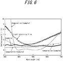
FIG. 6 is a graph illustrating reflectance (%) according to the wavelength of each laminate of Example 2-1 and Comparative Examples 2-1 to 2-4; and -
FIG. 7A is a graph illustrating reflectance (%) according to the wavelength of each laminate of Comparative Examples 1-4 to 1-7, andFIG. 7B is a graph illustrating reflectance (%) according to the wavelength of each laminate of Comparative Examples 1-1 to 1-7. - Hereinafter an embodiment of the present disclosure will be illustrated specifically with reference to drawings as necessary. Each member disclosed in
FIGS. 1 to 3 may be schematically represented by a scale or a shape different from the actual ones for convenience of explanation. - First, an embodiment of a laminate according to the present disclosure will be explained.
- The laminate according to the present disclosure is a laminate 1 including a
display plate 10, alight shielding film 20 provided on thedisplay plate 10 and ananti-reflection structure 30 having a fine uneven structure on a surface thereof, as illustrated inFIG. 1 . - In the laminate 1 according to the present disclosure, a part of the
light shielding film 20 has anon-light shielding portion 21 without thelight shielding film 20, theanti-reflection structure 30 is formed in thenon-light shielding portion 21 through anadhesion layer 40, the fineuneven structure 30 has an uneven period P equal to or less than the wavelength of visible light (seeFIG. 2 ), and a color difference (ΔE) between the reflected light by the light shielding film and the reflected light by the anti-reflection structure expressed in a formula shown below is equal to or less than 1.5.
- A high anti-reflection performance can be realized while thinning is achieved by forming an
anti-reflection structure 30 having a fine uneven structure on the surface thereof through theadhesion layer 40 and setting an uneven period P of the fineuneven structure 30 to be equal to or less than the wavelength of the visible light. Moreover, when a color difference ΔE between the reflected light by thelight shielding film 20 and the reflected light by theanti-reflection structure 30 is small such as equal to or less than 1.5, the reflection chromaticity can be kept neutral between the surface treated with the anti-reflection treatment technique (the surface of theanti-reflection structure 30 inFIG. 1 ) and its surrounding surface (the surface of thelight shielding film 20 inFIG. 1 ). - As illustrated in
FIG. 1 , the laminate 1 according to the present disclosure includes thedisplay plate 10. - The
display plate 10 is a member serving as a substrate or a support plate of the laminate 1 according to the present disclosure. Materials of thedisplay plate 10 are not particularly limited, and may be appropriately selected according to the purpose of use of the laminate. - For example, the material of the display plate may be glass, polymethyl methacrylate (PMMA) or the above described materials whose surface is coated with an organic material (polyimide, etc.), and the like. The display plate may preferably be transparent so as to transmit light, since the display plate is used as a liquid crystal display, a touch panel and the like.
- It is to be noted that, "transparent" herein means a transmittance of the light of the wavelength belonging to the visible light band (about 360 nm to 830 nm) is high, and for example, means that a transmittance of the light is equal to or greater than 70%.
- Furthermore, the shape of the display plate is not particularly limited except that it has a plate shape, and can be appropriately selected according to the purpose of use of the laminate. Further, the surface on which the light shielding film and the anti-reflection structure are laminated (in
FIG. 1 , under the display plate 10) may be a flat face, for example, so that they can be easily formed. - The laminate 1 according to the present disclosure further includes the
light shielding film 20 on thedisplay plate 10 as illustrated inFIG. 1 . - The
light shielding film 20 enhances the light-shielding effect, and blocks the light from reaching a solid-state image sensor even if a thinneddisplay plate 10 transmits the light (in particular the light with a wavelength of equal to or greater than 800 nm). - A material constituting the light shielding film is not particularly limited, and a known light shielding film can be appropriately used depending on the use.
- As a material of the light shielding film, for example, a composition for a light shielding film in which a binder resin contains light-shielding particles, a filler, other additives and the like can be used.
- Examples of the binder resin include, for example, (meth) acrylic resin, urethane resin, polyvinyl alcohol, polyvinyl butyral, polyvinyl formal, polyamide, polyester, and the like, and include (meth) acrylic resin, urethane resin, and the like. These resins may have a carboxylic acid group, a sulfonate group, a phonic acid group, a phonic acid group, a sulfonamide group, and the like, as an acid group,
- Examples of the light-shielding particles include, for example, inorganic pigment such as carbon black, titanium black, tungsten compound, zinc oxide, lead white, lithopon, titanium oxide, chromium oxide, iron oxide, precipitated barium sulfate and barite powder, red lead, red iron oxide, yellow lead, zinc yellow (zinc yellow type 1 and zinc yellow type 2), ultramarine blue, procyanide blue (potassium ferrocyanide), zircon gray, praseodymium yellow, chrome titanium yellow, chrome green, peacock, victorial green, iron blue (unrelated to Prussian blue), vanadium zirconium blue, chrome tin pink, manganese pink, salmon pink and the like. Further, as the black pigment, a metal oxide, a metal nitrogen, a mixture thereof, or the like containing one or more metal elements selected from the group consisting of Co, Cr, Cu, Mn, Ru, Fe, Ni, Sn, Ti, and Ag can be used.
- Furthermore, the light-shielding particles may also include light-shielding dyes such as, for example, cyanine dyes, phthalocyanine dyes, naphthalocyanine dyes, immonium dyes, aminium dyes, quinolium dyes, pyrylium dyes, or metal complex dyes such as Ni complex dyes.
- The content of the light-shielding particles in the light-shielding film composition is not particularly limited, but is preferably from 30 to 70 mass%, more preferably from 40 to 60 mass%, and still more preferably from 45 to 55 mass%, based on the total solid content.
- Further, the composition for a light shielding film may contain fillers and other additives as necessary. The filler is not particularly limited as long as it increases the reflectance, and for example, an organic filler, an inorganic filler, or an inorganic-organic composite filler can be used.
- Examples of the organic filler include, for example, synthetic resin particles, natural polymer particles, and the like, and preferably resin particles such as acrylic resin, polyethylene, polypropylene, polyethylene oxide, polypropylene oxide, polyethyleneimine, polystyrene, polyurethane, polyurea, polyester, polyamide, polyimide, carboxymethylcellulose, gelatin, starch, chitin, chitosan, and the like.
- Examples of the inorganic filler include metals and metal compounds such as silica, mica compound, glass, zinc oxide, alumina, zircon oxide, tin oxide, potassium titanate, strontium titanate, aluminum borate, magnesium oxide, magnesium borate, aluminum hydroxide, magnesium hydroxide, calcium hydroxide, titanium hydroxide, basic magnesium sulfate, calcium carbonate, magnesium carbonate, calcium sulfate, magnesium sulfate, calcium silicate, magnesium silicate, calcium phosphate, silicon nitride, titanium nitride, aluminum nitride, silicon carbide, titanium carbide, zinc sulfide, and at least two or more of these compounds.
- Examples of the above described other additives include known additives such as a polymerizable compound, a polymerization initiator, a dispersant, a sensitizer, a crosslinking agent effect accelerator, and a surfactant.
- Although the average thickness of the
light shielding film 20 is not particularly limited, it is preferably equal to or less than 30 µm, and more preferably equal to or less than 10 µm in terms of thinning of the laminate 1. Moreover, the thickness of thelight shielding film 20 is preferably equal to or greater than 3 µm in terms of maintaining a high light-shielding effect. - It is to be noted that the average thickness of the
light shielding film 20 is obtained by taking the average of the portion where thelight shielding film 20 is formed, excepting the thickness of thenon-light shielding portion 21 described later. For example, it can be obtained by taking the average of thicknesses of any five portions of thelight shielding film 20, for example. - Further, in the laminate 1 according to the present disclosure, as illustrated in
FIG. 1 , a part of thelight shielding film 20 is constituted of anon-light shielding portion 21 where nolight shielding film 20 is formed. This is because, when theanti-reflection structure 30 described later is provided in thenon-light shielding portion 21, thinning of the laminate 1 is promoted and an anti-reflection action can be sufficiently exhibited as well. - It is to be noted that the
non-light shielding portion 21 is a portion of thelight shielding film 20 where no light shielding film is formed. The above describednon-light shielding portion 21 may be a through hole as illustrated inFIG. 1 or a partially transparent material may be filled therein. - The size of the
non-light shielding portion 21 is not particularly limited, and may be changed according to the size of theanti-reflection structure 30. - However, it is preferable that the portion where the
anti-reflection structure 30 is not formed be as small as possible so as to reliably block the light reaching the solid-state image sensor. Specifically, when the light shielding film and thenon-light shielding portion 21 are viewed from the front, it is preferable that theanti-reflection structure 30 be formed in a range of preferably 50% and more preferably 100% of the area of the non-light shielding portion 21 (i.e., the opening area of the light shielding film 20). - The method of forming the
light shielding film 20 is not particularly limited, and a known forming method can be appropriately used depending on the thickness of thelight shielding film 20, the manufacturing facility, and the like. - For example, the light-shielding
film 20 can be formed by applying the above described light-shielding film composition to thedisplay plate 10 by spin coating, spray coating, slit coating, inkjet coating, rotation coating, flow casting coating, roll coating, screen printing, or the like, followed by curing treatment such as light irradiation treatment or heat treatment. - As illustrated in
FIG. 1 , the laminate 1 according to the present disclosure has, in thenon-light shielding portion 21 thereof, theanti-reflection structure 30 having a fine uneven structure formed on the surface thereof. - The
anti-reflection structure 30 can enhance the anti-reflection performance of the laminate 1 by the fine uneven structure formed on the surface thereof. -
FIG. 2A illustrates an embodiment of theanti-reflection structure 30 and theadhesion layer 40. - Each projection and each recess of the fine uneven structure of the
anti-reflection structure 30 may be periodically disposed (e.g., staggered lattice shape, rectangular lattice shape), as illustrated inFIG. 2A , and may also be disposed randomly. Furthermore, the shape of the projection and the recess is not particularly limited, and may be artillery, conical, columnar, or needle shaped and the like. It is to be noted that the shape of the recess means a shape formed by the inner wall of the recess. - The fine uneven structure of the
anti-reflection structure 30 has an uneven period (uneven pitch) P that is equal to or less than the wavelength of visible light (e.g. 830 nm or less). Moreover, the upper limit of the uneven period P is preferably equal to or less than 350 nm and more preferably equal to or less than 280 nm, and the lower limit of the uneven period P is preferably equal to or greater than 100 nm, and more preferably equal to or greater than 150 nm. - The uneven period P of the fine uneven structure is set to not more than the visible light wavelength, in other words, the fine uneven structure is formed in what is called a "moth-eye structure," and as a result an excellent anti-reflection performance can be realized.
- The uneven period P of the uneven structure is an arithmetic mean value of the distances between adjacent protrusions and adjacent recesses. The uneven period P can be observed, for example, using a scanning electron microscope (SEM) or a cross-section transmission electron microscope (cross-section TEM) and the like.
- The method by which the arithmetic mean value between adjacent protrusions and adjacent recesses is calculated may, for example, be a method in which a plurality of combinations of adjacent protrusions and a plurality of combinations of adjacent recesses are selected, the distances between the protrusions and the distances between the recesses in these combinations are measured, and the measured values are averaged.
- Further, the average uneven height (the depth of recess) H of the fine uneven structure may preferably be equal to or greater than 190 nm so as to keep the reflection chromaticity neutral in more reliable manner. Further, the average uneven height P of the fine uneven structure may preferably be equal to or less than 320 nm in terms of thinning of the laminate. As illustrated in
FIG. 2A , the uneven height H of the fine uneven structure is a distance from the bottom of the recess to the vertex of the protrusion, as illustrated inFIG. 2A , and the average uneven height can be obtained by measuring some uneven heights H (e. g., five portions) and averaging them. - The thickness of the support portion under the fine uneven structure of the
anti-reflection structure 30 where the fine uneven structure is not formed (hereinafter referred to as a "base portion" of the anti-reflection structure 30) is not particularly limited, and may be about from 500 nm to 9000 nm. - The fine uneven structure of the
anti-reflection structure 30 is needed to be provided on the surface on the side that does not come in contact with at least theadhesion layer 40, as illustrated inFIG. 2A . However, as another embodiment, the fine uneven structure can be provided on both sides, as illustrated inFIG. 2B . - The material of the
anti-reflection structure 30 is not particularly limited. Examples of the material include, for example, a resin composition that is cured by a curing reaction, such as an active energy ray curable resin composition (photocurable resin composition, electron beam curable resin composition), thermosetting resin composition, or the like, and for example, a resin composition containing a polymerizable compound and a polymerization initiator. - As the polymerizable compound, for example, (i) an esterified product obtained by reacting (meth) acrylic acid or a derivative thereof in a ratio of equal to or greater than 2 mol to 1 mol of polyhydric alcohol, (ii) an esterified product obtained by a polyhydric alcohol, a polyvalent carboxylic acid or an anhydride thereof, an (meth)acrylic acid or a derivative thereof, and the like can be used.
- Examples of the above described (i) include 1,4-butanediol di(meth)acrylate, 1,6-hexanediol di(meth)acrylate, 1,9-nonanediol di(meth)acrylate, trimethylol propantri(meth)acrylate, trimethylol ethantri(meth)acrylate, pentaerythritol tri(meth)acrylate, pentaerythritol tetra(meth)acrylate, tetrahydrofuryl acrylate, glycerin tri(meth)acrylate, dipentaerythritol penta(meth)acrylate, dipentaerythritol hexa(meth)acrylate, tripentaerythritol hexa(meth)acrylate, tripentaerythritol hepta(meth)acrylate, acryloimonofoline, urethane acrylate, and the like.
- Examples of the above described (ii) include polyhydric alcohols such as trimethylolethane, trimethylolpropane, glycerin, and pentaerythritol; polycarboxylic acids or anhydrides thereof selected from malonic acid, succinic acid, adipic acid, glutaric acid, sebacic acid, fumaric acid, itaconic acid, maleic anhydride, and the like; and esterified products obtained by reacting (meth)acrylic acid or derivatives thereof.
- These polymerizable compounds may be used alone or two or more types may be used in combination.
- Furthermore, when the resin composition is photocurable, examples of photopolymerization initiators include, for example: carbonyl compounds such as benzoin, benzoin methyl ether, benzoin ethyl ether, benzoin isopropyl ether, benzoin isobutyl ether, benzyl, benzophenone, p-methoxybenzophenone, 2,2-diethoxyacetophenone, α, α-dimethoxy-α-phenylacetophenone, methylphen ylglyoxylate, ethylphenylglyoxylate, 4,4'-bis(dimethylamino)benzophenone, 1-hydroxycyclohexyl phenyl ketone, 2-hydroxy-2-methyl-1-phenyl-propan-1-one, and the like; sulfur compounds such as tetramethylthiuram monosulphide, tetramethylthiuram disulfide, and the like; 2,4,6-trimethylbenzoyl diphenyl-phosphine oxide, benzoyl diethoxyphosphine oxide; and the like. One or more of these can be used.
- When the resin composition is electron beam curable, examples of the electron beam polymerization initiator include: thioxanthones such as benzophenone, 4,4-bis(di ethylamino)benzophenone, 2,4,6-trimethylbenzophenone, methylorthobenzoylbenzoate, 4-phenylbenzophenone, t-butylanthraquinone, 2-ethylanthraquinone, 2,4-diethylthioxanthone, isopropylthioxanthone, 2,4-dichlorothioxanthone, and the like; acetophenones such as diethoxyacetophenone, 2-hydroxy-2-methyl-1-phenylpro pane-1-one, benzyl dimethyl ketal, 1-hydroxycyclohexyl-phenyl ketone, 2-methyl-2 -morpholino(4-thiomethylphenyl)propane-1-one, 2-benzyl-2-dimethylamino-1-(4-morpholinophenyl)-butanone; benzoin ethers such as benzoin methyl ether, benzoin ethyl ether, benzoin isopropyl ether, and benzoin isobutyl ether; acylphosphine oxide such as 2,4,6-trimethylbenzoyldiphenylphosphine oxide, bis(2,6-dimethoxybenzoyl)-2,4, 4-trimethylpentylphosphine oxide, bis(2,4,6-trimethylbenzoyl)-phenylphosphine oxide, and the like; and methylbenzoyl formate, 1,7-bisacridinylheptane, 9-phenylacrydin, and the like. One or more of these can be used.
- When the resin composition is thermosetting, examples of thermal polymerization initiators include: organic peroxides such as methyl ethyl ketone peroxide, benzoyl peroxide, dicumyl peroxide, t-butyl hydroperoxide, cumene hydroperoxide, t-butyl peroxyoctoate, t-butyl peroxybenzoate, lauroyl peroxide, and the like; azo-based compounds such as azobisisobutyronitrile; and redox polymerization initiators obtained by combining amines such as N,N-dimeth ylaniline, N,N-dimethyl-p-toluidine with the above described organic peroxides.
- These photopolymerization initiators, electron beam polymerization initiators, and thermal polymerization initiators may be used alone or in combination as desired.
- The amount of polymerization initiator is preferably 0.01 to 10 parts by mass with respect to 100 parts by mass of polymerizable compound. In such a range, the curing proceeds sufficiently, the molecular weight of the cured product becomes appropriate, and sufficient strength is obtained, and there is no problem that the cured product is colored due to the residue of the polymerization initiator or the like.
- Moreover, the resin composition may contain a non-reactive polymer or an active energy ray sol-gel reactive component, and may contain various additives such as a thickener, a leveling agent, an ultraviolet absorber, a light stabilizer, a thermal stabilizer, a solvent, an inorganic filler, and the like, as necessary.
- The method of producing the
anti-reflection structure 30 is not particularly limited. For example, as illustrated inFIGS. 3A to 3C , anantireflection structure 30 having a fine uneven structure on the surface thereof can be obtained by performing a clamping/crimping step, a curing step, and a peeling step. - In the clamping/crimping step, as illustrated in
FIG. 3A , a resin composition for anti-reflection structure is clamped and crimped between a holding film having a fine uneven structure on the surface thereof and a holding film having a flat surface. - Specifically, first, a holding film having a fine uneven structure on the surface thereof (a
first holding film 201a) and a holding film having a flat surface (asecond holding film 201b) are provided. Subsequently, as illustrated inFIG. 3A , a resin composition foranti-reflection structure 151 is clamped between thefirst holding film 201a and thesecond holding film 201b. It is to be noted that the holdingfilm 201a having a fine uneven structure on the surface thereof can be produced by forming a fine uneven layer having a predetermined recess-protrusion pattern on a base substrate made of a transparent and hard to break material (e.g., polyethylene terephthalate, triacetyl cellulose, etc.). Thereafter, as illustrated inFIG. 3A , the clamped body is crimped in the clamping direction by a crimpingapparatus 160 such as a roll laminator, and the like. Here, in the clamping/crimping step, the thickness of theanti-reflection structure 30 that is obtained finally can be adjusted by adjusting the pressure during crimping. - In the above described curing step, as illustrated in
FIG. 3B , the clamped resin composition foranti-reflection structure 151 is cured by irradiating with active energy rays such as UV light to form theanti-reflection structure 30 having a fine uneven structure on both sides theteof. - Specifically, as illustrated in
FIG. 3B , the clamped resin composition foranti-reflection structure 151 is irradiated with active energy rays to cure the resin composition foranti-reflection structure 151. When the resin composition foranti-reflection structure 151 is cured, a holdingfilm laminate 250 including theanti-reflection structure 30 having a fine uneven structure on the surface thereof is obtained. It is to be noted that the curing step may be performed at the same timing as that of the clamping/crimping step. - In the peeling step, as illustrated in
FIG. 3C , the holdingfilms film laminate 250 to obtain theanti-reflection structure 30. - The obtained
anti-reflection structure 30 is subjected to a treatment such as cleaning or the like as necessary. - The method of producing the
anti-reflection structure 30 is not limited to the above described method of performing a clamping/crimping step, a curing step and a peeling step (FIGS. 3A to 3C ), and theanti-reflection structure 30 can be produced by forming a fine uneven structure by sputtering and the like after the resin composition for anti-reflection structure is cured, for example. - The laminate 1 according to the present disclosure further includes an
adhesion layer 40 configured to bond theanti-reflection structure 30 to thenon-light shielding portion 21, as illustrated inFIG. 1 . - The
adhesion layer 40 is made of an adhesive in order to bond theanti-reflection structure 30 to thenon-light shielding portion 21. However, it is necessary to use a material that does not deteriorate the anti-reflection performance of theanti-reflection structure 30. - Specific materials are not particularly limited, and resin compositions which are cured by a curing reaction can be used as appropriate. Among them, the
adhesive layer 40 is preferably made of an ultraviolet curable adhesive to obtain a high bonding property. Examples of the ultraviolet curable resin include an ultraviolet curable acrylic resin, an ultraviolet curable epoxy resin, and the like. - The method of forming the
adhesion layer 40 is not particularly limited. For example, when theadhesion layer 40 is a layer made of an ultraviolet curable adhesive, theadhesion layer 40 can be formed by irradiating ultraviolet rays to thenon-light shielding portion 21 in a state where the ultraviolet curable adhesive is crimped with theanti-reflection structure 30. - It is preferable that the
adhesion layer 40 is thinned in a range in which a high bonding property can be maintained in terms of thinning the laminate 1. - Specifically, as illustrated in
FIGS. 2A and 2B , a total thickness T of theanti-reflection structure 30 and theadhesion layer 40 may preferably be equal to or less than 30 µm, and more preferably be equal to or less than 10 µm. - (Color difference between reflected light by light shielding film and reflected light by anti-reflection structure: ΔE)
- According to the laminate 1 of the present disclosure, a color difference (ΔE) between the reflected light by the
light shielding film 20 and the reflected light by theanti-reflection structure 30 expressed in the a formula shown below is equal to or less than 1.5.
- When the color difference (ΔE) between the reflected light by the
light shielding film 20 and the reflected light by theanti-reflection structure 30 is equal to or less than 1.5, a reflection chromaticity can be kept neutral between the surface of theanti-reflection structure 30 and its surrounding surface (inFIG. 1 , the surface of the light shielding film 20). Thus, when the laminate according to the present disclosure is used for the camera module mounting apparatus, a captured image with reduced color unevenness can be obtained. - In the above formula, a1 and b1 represent a* and b* values of the light reflected by the
light shielding film 20 in the CIE1976 (L *a*b*) color system, and a2 and b2 represent a* and b* values of the light reflected by theanti-reflection structure 30 in the CIE1976 (L *a*b*) color system. The CIE1976 (L*a*b*) color system is one of the uniform color spaces defined by CIE in 1976, and a color space using three-dimensional orthogonal coordinates of the lightness index L and the chromaticity indices a* and b* is called an L*a*b* color space, and is a color system using this color space. - Although the ΔE needs to be equal to or less than 1.5, in terms of making the reflection chromaticity of the surface of the
anti-reflection structure 30 and its surrounding surface more neutral, it is preferably equal to or less than 1.0, and more preferably equal to or less than 0.7. - The a* value and b* values of the light reflected by the
light shielding film 20 in the CIE1976 (L *a*b*) color system and a* value and b* values of the light reflected by theanti-reflection structure 30 in the CIE1976 (L *a*b*) color system can be obtained by using commercially available measuring devices. - The above described a* value and b* value in the CIE1976 (L*a*b*) color system and the color difference ΔE can be adjusted by changing the material, the shape and the thickness of the
light shielding film 20, the material of theanti-reflection structure 30, the uneven period P of the uneven structure, the uneven height H of the uneven structure, and the like. - Furthermore, according to the laminate 1 of the present disclosure, the difference (ΔY) between the luminous reflectance (Y value) of the
light shielding film 20 and the luminous reflectance (Y value) of theanti-reflection structure 30 is preferably equal to or less than 0.5. This is because, since the brightness on the chromaticity diagram can be set substantially the same condition, the reflection chromaticity between the surface of theanti-reflection structure 30 and its surrounding surface can be maintained more neutral. - Here, the luminous reflectance (Y value) is a reflectance obtained in consideration that the brightness perceived by eyes is changed by the visibility sensitivity, and is (X, Y, Z) when representing the color of the positive reflected light in the CIE1931 XYZ color space, or (x, y, Y) when representing the color of the positive reflected light in the CIE xyY color space. The visual reflectance can be measured with a commercially available spectrometer (e.g., V650, etc., from JASCO Corporation).
- It is to be noted that the luminous reflectance and the difference in reflectance of each of the light shielding film and the
anti-reflection structure 30 can be adjusted by changing the density or the uneven height of the fine uneven structure, for example. - The camera
module mounting apparatus 300 according to the present disclosure includes a laminate 1 according to the present disclosure and acamera module 310 provided at a position facing theanti-reflection structure 30 in the laminate, as illustrated inFIG. 4 . - According to the camera module mounting apparatus of the present disclosure, a still image or a moving image can be photographed by an image sensor of the camera module through the laminate of the present disclosure, thus reflection of light is suppressed, and occurrence of color unevenness and the like can be suppressed in a captured image obtained.
- Next, the present disclosure will be explained in more detail on the basis of examples. However, the present disclosure is not limited in any manner to the following examples.
- A model of the laminate 1 including a
display plate 10, alight shielding film 20 provided on thedisplay plate 10 and ananti-reflection structure 30 having a fine uneven structure on the surface thereof was produced as illustrated inFIG. 1 . For each of thelight shielding film 20 and theanti-reflection structure 30, the chromaticity of reflected light (irradiation angle : 5°) was calculated. - Here, the
display plate 10 was a glass substrate, and thelight shielding film 20 contained carbon black, and was formed by applying a spray paint containing butyl acetate, ethyl acetate, nitrocellulose, diisobutyl ketone, isopropyl alcohol, isobutanol, and the like to the surface of the glass substrate. Theanti-reflection structure 30 was formed of "UVX-6366" (ultraviolet curable resins consisting of 1,6-hexanediol diacrylate, tetrahydrofuryl acrylate, and 2,4,6-trimethylbenzoyl diphenyl phosphine oxide) from TOAGOSEI CO., LTD., and had an uneven period of the fine uneven structure of 150 to 250 nm, an uneven height of 220 nm, a thickness of the base portion without the fine uneven structure of 1000nm, and a refractive index n = 1.520. Moreover, ultraviolet curing resin is used for theadhesion layer 40, and a thickness thereof was 3000 nm. A total thickness of theanti-reflection structure 30 and theadhesion layer 40 was 4220 nm (about 4.2 µm). - Table 1 shows the structure of the antireflection structure, the total thickness (µm) of the anti-reflection structure and the adhesive layer, and the calculation results of the a* value and the b* value (a2 and b2) of the light reflected by the anti-reflection structure in the CIE1976 (L*a*b*) color system and the color difference ΔE between the reflected light by the light shielding film and the reflected light by the anti-reflection structure.
- In Comparative Example 1-1, a laminate was produced under the same conditions as in Example 1-1 except that, as an anti-reflection technique, an anti-reflection film (Dry-AR direct forming) was formed by alternately laminating four layers in total of NbOx and SiO2 instead of the
anti-reflection structure 30 having a fine uneven structure. - Table 1 shows the antireflection structure, the total thickness (µm) of the anti-reflection structure and the adhesive layer, and the calculation results of the a* value and the b* value of the light reflected by the anti-reflection structure in the CIE1976 (L*a*b*) color system and the color difference ΔE between the reflected light by the light shielding film and the reflected light by the anti-reflection structure.
- In Comparative Example 1-2, a laminate was produced under the same conditions as in Example 1-1 except that, as an anti-reflection technique, an anti-reflection film (Wet-AR direct coating) was formed by coating a material having a refractive index n = 1.340.
- Table 1 shows the antireflection structure, the total thickness (µm) of the anti-reflection structure and the adhesive layer, and the calculation results of the a* value and the b* value of the light reflected by the anti-reflection structure in the CIE1976 (L*a*b*) color system and the color difference ΔE between the reflected light by the light shielding film and the reflected light by the anti-reflection structure.
- In Comparative Example 1-3, a laminate was produced under the same conditions as in Example 1-1 except that, as an anti-reflection technique, an antireflection film (Wet-AR film lamination) was formed by laminating a high refractive index material (refractive index n = 1.700) and a low refractive index material (refractive index n = 1.250).
- Table 1 shows the antireflection structure, the total thickness (µm) of the anti-reflection structure and the adhesive layer, and the calculation results of the a* value and the b* value of the light reflected by the anti-reflection structure in the CIE1976 (L*a*b*) color system and the color difference ΔE between the reflected light by the light shielding film and the reflected light by the anti-reflection structure.
- In Examples 1-2 to 1-7 and Comparative Examples 1-4 to 1-7, a laminate was produced under the same conditions as in Example 1-1 except that the uneven height was changed (for specific height of the uneven height, see Table 2) with respect to the fine uneven structure of the
anti-reflection structure 30. - Table 3 shows an uneven height (nm) of the anti-reflection structure, the a* value and the b* value of the light reflected by the anti-reflection structure in the CIE1976 (L*a*b*), and the color difference ΔE between the reflected light by the light shielding film and the reflected light by the anti-reflection structure (Dry-AR direct forming).
- As illustrated in
FIG. 1 , a laminate 1 including adisplay plate 10, alight shielding film 20 provided on thedisplay plate 10 and ananti-reflection structure 30 having a fine uneven structure on the surface thereof was actually produced. For each of thelight shielding film 20 and theanti-reflection structure 30, the chromaticity of each reflected light (irradiation angle : 5 °) was measured. - Here, the
display plate 10 was a glass substrate, and thelight shielding film 20 contained carbon black, and was formed by applying a spray paint containing butyl acetate, ethyl acetate, nitrocellulose, diisobutyl ketone, isopropyl alcohol, isobutanol, and the like to the surface of the glass substrate. Theanti-reflection structure 30 was formed of "UVX-6366" (ultraviolet curable resins consisting of 1,6-hexanediol diacrylate, tetrahydrofuryl acrylate, and 2,4,6-trimethylbenzoyl diphenyl phosphine oxide) from TOAGOSEI CO., LTD., and had an uneven period of the fine uneven structure of 150 to 250 nm, an uneven height of 220 nm, a thickness of the base portion without the fine uneven structure of 1000nm. Moreover, ultraviolet curing resin is used for theadhesion layer 40, and a thickness thereof was 3780 nm. A total thickness of theanti-reflection structure 30 and theadhesion layer 40 is 5000 nm (5 ¡.tm). - Table 2 shows a structure of the antireflection structure, the total thickness (µm) of the anti-reflection structure and the adhesive layer, and the calculation results of the a* value and the b* value of the light reflected by the anti-reflection structure in the CIE1976 (L*a*b*) and the color difference ΔE between the reflected light by the light shielding film and the reflected light by the anti-reflection structure.
- Each laminate sample obtained by Examples and Comparative Examples was evaluated as follows. Evaluation results are shown in Table 1.
-
- (a) The spectral wavelength and the reflectance (5°) of each sample of Examples 1-1 and Comparative Examples 1-1 to 1-3 were calculated using the calculation software "TFCalc." The relationship between the wavelength and the reflectance is shown in
FIG. 5 . For reference, the relationship between the wavelength of the light shielding film portion and the reflectance is also shown inFIG. 5 .
From the results ofFIG. 5 , it was found that the anti-reflection performance of the laminate of Example 1-1 was the best in the wavelength range of 420 to 620 nm. - (b) The spectral wavelength and the reflectance (5°) of the sample of Example 1-2 were measured by using an ultraviolet visible near-infrared spectrophotometer "V-650" from JASCO Corporation.
FIG. 6 shows the relationship between the wavelength and the reflectance. For reference, the relationship between the wavelength and the reflectance of each sample of Comparative Examples 1-1 to 1-3 and the light shielding film portion is also shown inFIG. 6 .
From the results ofFIG. 6 , it was found that the anti-reflection performance of the actually produced laminate of Example 2 was also excellent in the wavelength range of 420 to 660 nm as with Example 1-1. - (a) The a* value and the b* value of the light reflected by the anti-reflection structure in the CIE1976 (L*a*b*), and the color difference ΔE between the reflected light by the light shielding film and the reflected light by the anti-reflection structure were calculated using the calculation software "TFCalc" with respect to each sample of Example 1-1 and Comparative Examples 1-1 to 1-3. The calculation results are shown in Table 1.
- Table 1 shows that the ΔE of Example 1-1 is the smallest, and the reflection chromaticity is kept neutral. (b) With respect to the sample of Example 2, the optical spectrum was obtained by using an ultraviolet visible near-infrared spectrophotometer "V-650" from JASCO Corporation, and on the basis of that, the a* value and the b* value of the light reflected by the anti-reflection structure in the CIE1976 (L*a*b*) and the color difference ΔE between the reflected light by the light shielding film and the reflected light by the anti-reflection structure were calculated. The measuring results are shown in Table 2.
- Table 2 shows that ΔE is kept small, and the reflection chromaticity is kept neutral with respect to Example 2, as with Example 1-1.
- The spectral wavelength and reflectance (5°) of each sample of Examples 1-2 to 1-7 and Comparative Examples 1-4 to 1-7 were calculated using the calculation software "TFCalc," and the relationship between the wavelength and the reflectance is shown in
FIGS. 7A and 7B . Furthermore, the a* value and the b* value of the light reflected by the anti-reflection structure in the CIE1976 (L*a*b*), and the color difference ΔE between the reflected light by the light shielding film and the reflected light by the anti-reflection structure were also calculated, and the calculation results are shown inFIG. 3 . It is to be noted that, when the color difference ΔE obtained from the calculation was equal to or less than 1.5, which was within a range of the present disclosure, it was evaluated as "pass," and when it exceeded 1.5, it was evaluated as "fail." The evaluation results are shown in Table 3. -
FIG. 7 and Table 3 show that, when the uneven height of the uneven structure is equal to or greater than 190 nm, ΔE can be kept within the range of the present disclosure (the determination result is "pass"). Thus an excellent anti-reflection performance could be realized, and reflection chromaticity could be kept neutral.[Table 1] Example 1-1 Comparative Example 1-1 Comparative Example 1-2 Comparative Example 1-3 Light shielding film (reference) Structure of anti-reflection structure Fine uneven structure Dry-AR direct forming Wet-AR direct coating Wet-AR film lamination - Total thickness of anti-reflection structure and adhesion layer 4.2 µm 0.2 µm 0.1 µm 65 µm - a* value of the light reflected by the anti-reflection structure 0.43 4.22 0.98 3.56 -0.1 b* value of the light reflected by the anti-reflection structure -0.59 -7.13 -1.45 -4.95 -0.28 Color difference between reflected light by light shielding film and reflected light by anti-reflection structure: ΔE 0.61 8.11 1.59 5.94 0 Determination Pass Fail Fail Fail - [Table 2] Example 2 Structure of anti-reflection structure Fine uneven structure Total thickness of anti-reflection structure and adhesion laver 5 µm a* value of the light reflected by the anti-reflection structure -0.33 b* value of the light reflected by the anti-reflection structure -051 Color difference between reflected light by light shielding film and reflected light bv anti-reflection structure: ΔE 0.33 Determination Pass [Table 3] Cmparative Example 1-4 Cmparative Example 1-5 Cmparative Example 1-6 Cmparative Example 1-7 Example 1-2 Example 1-3 Example 1-4 Example 1-1 Example 1-5 Example 1-6 Example 1-7 Total thickness of anti-reflection structure and adhesion layer 80nm 120nm 160nm 180nm 190nm 200nm 210nm 220nm 240nm 280nm 320nm Total thickness of anti-reflection structure and adhesion layer 0.15 0.59 0.95 0.94 0.87 0.75 0.6 0.43 0.05 -0.48 -0.39 a* value of the light reflected by the anti-reflection structure 2.23 3.13 2.09 1.05 0.53 0.07 -0.31 -0.59 -0.82 -0.26 0.61 b* value of the light reflected by the anti-reflection structure 2.51 3.47 2.59 1.69 1.26 0.92 0.7 0.61 0.56 0.38 0.93 Color difference between reflected light by light shielding film and reflected light by anti-reflection structure: ΔE Fail Fail Fail Fail Pass Pass Pass Pass Pass Pass Pass - According to the present disclosure, a laminate and an anti-reflection structure that can be thinned, are excellent in anti-reflection performance and can keep reflection chromaticity neutral can be provided. Further, according to the present disclosure, a camera module mounting apparatus can be provided, in which thinning is achieved by using the laminate and a captured image with reduced color unevenness can be obtained.
-
- 1
- Laminate
- 10
- Display plate
- 20
- Light shielding film
- 21
- Non-light shielding portion
- 30
- Anti-reflection structure
- 40
- Adhesion layer
- 201a
- First holding film
- 201b
- Second holding film
- 250
- Holding film laminate
- 300
- Camera module mounting apparatus
- 310
- Camera module
Claims (7)
- A laminate comprising a display plate, a light shielding film provided on the display plate and an anti-reflection structure having a fine uneven structure on a surface thereof, wherein,
a part of the light shielding film has a non-light shielding portion without a light shielding film;
the anti-reflection structure is formed in the non-light shielding portion through an adhesion layer, and the fine uneven structure has an uneven period that is equal to or less than a wavelength of visible light; and
a color difference (ΔE) between a reflected light by the light shielding film and a reflected light by the anti-reflection structure expressed in a formula shown below is equal to or less than 1.5.
- The laminate according to claim 1, wherein a total thickness of the anti-reflection structure and the adhesion layer is equal to or less than 30 µm.
- The laminate according to claim 1 or 2, wherein the adhesion layer is a layer made of ultraviolet curing adhesive.
- The laminate according to any one of claims 1 to 3, wherein an average uneven height of the fine uneven structure is equal to or greater than 190 nm.
- The laminate according to any one of claims 1 to 4, wherein a difference (ΔY) between a luminous reflectance of the light shielding film and a luminous reflectance of the anti-reflection structure is equal to or less than 0.5.
- An anti-reflection structure formed on a display plate through an adhesion layer and having a fine uneven structure on a surface thereof, wherein,
the fine uneven structure has an uneven period that is equal to or less than a wavelength of visible light;
a total thickness of the anti-reflection structure and the adhesion layer is equal to or less than 30 µm; and
an average uneven height of the fine uneven structure is equal to or greater than 190 nm. - A camera module mounting apparatus, comprising a laminate according to any one of claims 1 to 5 and a camera module provided at a position facing an anti-reflection structure in the laminate.
Applications Claiming Priority (2)
| Application Number | Priority Date | Filing Date | Title |
|---|---|---|---|
| JP2017214809A JP7025892B2 (en) | 2017-11-07 | 2017-11-07 | Laminates, anti-reflection structures and camera module mounting devices |
| PCT/JP2018/039990 WO2019093164A1 (en) | 2017-11-07 | 2018-10-26 | Laminated body, antireflection structure, and camera module mounting device |
Publications (3)
| Publication Number | Publication Date |
|---|---|
| EP3708358A1 true EP3708358A1 (en) | 2020-09-16 |
| EP3708358A4 EP3708358A4 (en) | 2021-08-11 |
| EP3708358B1 EP3708358B1 (en) | 2022-11-16 |
Family
ID=66438300
Family Applications (1)
| Application Number | Title | Priority Date | Filing Date |
|---|---|---|---|
| EP18877179.4A Active EP3708358B1 (en) | 2017-11-07 | 2018-10-26 | Laminated body, antireflection structure, and camera module mounting device |
Country Status (9)
| Country | Link |
|---|---|
| US (1) | US11614568B2 (en) |
| EP (1) | EP3708358B1 (en) |
| JP (3) | JP7025892B2 (en) |
| KR (1) | KR102694084B1 (en) |
| CN (1) | CN111316136B (en) |
| HU (1) | HUE060588T2 (en) |
| PL (1) | PL3708358T3 (en) |
| TW (1) | TWI795456B (en) |
| WO (1) | WO2019093164A1 (en) |
Families Citing this family (4)
| Publication number | Priority date | Publication date | Assignee | Title |
|---|---|---|---|---|
| JP2021056305A (en) * | 2019-09-27 | 2021-04-08 | デクセリアルズ株式会社 | Antireflection structure, base material with antireflection structure, camera module, and information terminal apparatus |
| KR102867994B1 (en) | 2020-11-24 | 2025-10-02 | 삼성디스플레이 주식회사 | Display apparatus and manufacturing the same |
| CN116113263A (en) * | 2023-03-21 | 2023-05-12 | 昆山国显光电有限公司 | Display panel and display device |
| WO2026063374A1 (en) * | 2024-09-18 | 2026-03-26 | 株式会社カネカ | Display module, electronic device, display module manufacturing method, and electronic device manufacturing method |
Family Cites Families (32)
| Publication number | Priority date | Publication date | Assignee | Title |
|---|---|---|---|---|
| JP2565525B2 (en) * | 1988-01-12 | 1996-12-18 | 日本板硝子株式会社 | Anti-reflection film attached transparent plate with metal film |
| JPH0961602A (en) * | 1995-08-28 | 1997-03-07 | Toyo Metallizing Co Ltd | Plastic optical article having antireflection film |
| JP5030386B2 (en) | 2005-03-03 | 2012-09-19 | 富士フイルム株式会社 | Light shielding film for display device, fine particle-containing composition for black material, material, substrate with light shielding film, color filter, liquid crystal display element, liquid crystal display device, and display device |
| EP1890172A4 (en) | 2005-06-09 | 2009-03-11 | Hitachi Chemical Co Ltd | METHOD FOR FORMING ANTIREFLECTION FILM |
| JP2008058723A (en) * | 2006-08-31 | 2008-03-13 | Sharp Corp | Anti-glare film and liquid crystal display device |
| WO2010032610A1 (en) * | 2008-09-17 | 2010-03-25 | シャープ株式会社 | Antireflection film and method for manufacturing same |
| JP4846867B2 (en) * | 2010-03-31 | 2011-12-28 | 三菱レイヨン株式会社 | Laminated body and method for producing the same |
| JP5586017B2 (en) * | 2010-08-20 | 2014-09-10 | 東海光学株式会社 | Optical products and eyeglass plastic lenses |
| JP5906572B2 (en) * | 2010-12-27 | 2016-04-20 | 大日本印刷株式会社 | Manufacturing method of display front plate and manufacturing method of display device |
| JP2012252224A (en) | 2011-06-03 | 2012-12-20 | Dainippon Printing Co Ltd | Antireflection film |
| JP2013018910A (en) * | 2011-07-13 | 2013-01-31 | Asahi Kasei E-Materials Corp | Resin cured product |
| JP6044544B2 (en) * | 2012-06-20 | 2016-12-14 | 三菱レイヨン株式会社 | Manufacturing method of laminate |
| US20150217532A1 (en) * | 2012-09-13 | 2015-08-06 | Toray Industries, Inc. | Method of manufacturing a laminate provided with a concave-convex structure and transfer film |
| JP2014071292A (en) * | 2012-09-28 | 2014-04-21 | Dainippon Printing Co Ltd | Anti-reflection article |
| JP5678941B2 (en) * | 2012-10-31 | 2015-03-04 | 大日本印刷株式会社 | Antireflection transparent conductive film, touch panel and image display device |
| JP5641036B2 (en) | 2012-11-15 | 2014-12-17 | 大日本印刷株式会社 | Antireflection article and image display device |
| WO2014163185A1 (en) * | 2013-04-05 | 2014-10-09 | 三菱レイヨン株式会社 | Microrelief structural body, decorative sheet, decorative resin molded body, method for producing microrelief structural body, and method for producing decorative resin molded body |
| JP6361162B2 (en) * | 2013-04-23 | 2018-07-25 | Agc株式会社 | Manufacturing method of glass substrate with double-sided low reflection film |
| CN105451967B (en) * | 2013-08-14 | 2017-11-10 | 三菱化学株式会社 | Manufacturing method of mold for nanoimprinting and antireflection article |
| US9577164B2 (en) | 2013-08-30 | 2017-02-21 | Asahi Kasei E-Materials Corporation | Semiconductor light emitting device and optical film |
| JP2015054402A (en) * | 2013-09-10 | 2015-03-23 | 三菱レイヨン株式会社 | Laminated structure, method for producing the same, and antireflection article |
| JP6354357B2 (en) | 2014-06-11 | 2018-07-11 | 三菱ケミカル株式会社 | Method for producing light transmissive film |
| JP6385181B2 (en) * | 2014-07-23 | 2018-09-05 | アキレス株式会社 | Transparent conductive film with sufficiently suppressed bone appearance |
| JP2016057335A (en) * | 2014-09-05 | 2016-04-21 | ソニー株式会社 | Laminate, imaging device package, image acquisition apparatus, and electronic equipment |
| JP6458481B2 (en) | 2014-12-16 | 2019-01-30 | 大日本印刷株式会社 | Anti-reflective articles and art exhibits |
| JP6234970B2 (en) * | 2015-07-22 | 2017-11-22 | 日東電工株式会社 | Cover member with transparent conductive layer having transparent adhesive layer |
| EP3264144B1 (en) * | 2015-07-24 | 2022-12-28 | Huawei Technologies Co., Ltd. | Camera module and terminal |
| JP6923293B2 (en) * | 2015-09-24 | 2021-08-18 | 三菱ケミカル株式会社 | Fine concavo-convex structure and joint |
| JP6633408B2 (en) | 2016-02-12 | 2020-01-22 | パナソニック インテレクチュアル プロパティ コーポレーション オブ アメリカPanasonic Intellectual Property Corporation of America | Control method, control device and equipment |
| JP2017146467A (en) | 2016-02-17 | 2017-08-24 | 大日本印刷株式会社 | Anti-reflection transparent plate |
| JP6786248B2 (en) * | 2016-04-12 | 2020-11-18 | キヤノン株式会社 | Optical element and its manufacturing method |
| JP6971587B2 (en) * | 2017-02-27 | 2021-11-24 | キヤノン株式会社 | Optical elements and their manufacturing methods, optical equipment |
-
2017
- 2017-11-07 JP JP2017214809A patent/JP7025892B2/en active Active
-
2018
- 2018-10-26 KR KR1020207012562A patent/KR102694084B1/en active Active
- 2018-10-26 HU HUE18877179A patent/HUE060588T2/en unknown
- 2018-10-26 WO PCT/JP2018/039990 patent/WO2019093164A1/en not_active Ceased
- 2018-10-26 PL PL18877179.4T patent/PL3708358T3/en unknown
- 2018-10-26 CN CN201880071894.XA patent/CN111316136B/en active Active
- 2018-10-26 EP EP18877179.4A patent/EP3708358B1/en active Active
- 2018-10-26 US US16/760,907 patent/US11614568B2/en active Active
- 2018-11-01 TW TW107138833A patent/TWI795456B/en active
-
2022
- 2022-02-14 JP JP2022020861A patent/JP2022066232A/en active Pending
-
2024
- 2024-06-05 JP JP2024091814A patent/JP2024107147A/en active Pending
Also Published As
| Publication number | Publication date |
|---|---|
| US20210132257A1 (en) | 2021-05-06 |
| EP3708358A4 (en) | 2021-08-11 |
| KR20200085750A (en) | 2020-07-15 |
| US11614568B2 (en) | 2023-03-28 |
| WO2019093164A1 (en) | 2019-05-16 |
| CN111316136A (en) | 2020-06-19 |
| TW201927545A (en) | 2019-07-16 |
| TWI795456B (en) | 2023-03-11 |
| JP2019084753A (en) | 2019-06-06 |
| EP3708358B1 (en) | 2022-11-16 |
| JP7025892B2 (en) | 2022-02-25 |
| CN111316136B (en) | 2022-05-31 |
| PL3708358T3 (en) | 2023-03-20 |
| JP2024107147A (en) | 2024-08-08 |
| HUE060588T2 (en) | 2023-03-28 |
| KR102694084B1 (en) | 2024-08-09 |
| JP2022066232A (en) | 2022-04-28 |
Similar Documents
| Publication | Publication Date | Title |
|---|---|---|
| EP3708358B1 (en) | Laminated body, antireflection structure, and camera module mounting device | |
| JP5365197B2 (en) | Near-infrared absorbing composition and near-infrared absorbing filter | |
| TWI454725B (en) | Optical laminate film | |
| US11874437B2 (en) | Black structure and self-luminous image display device comprising same | |
| JP5232448B2 (en) | Anti-glare material | |
| CN1433263A (en) | Electromagnetic wave shielding sheet | |
| JP2010025959A (en) | Optical filter for display, display with the same, and plasma display panel | |
| JP2011154211A (en) | Composite filter for front of image display device | |
| US20090059408A1 (en) | Optical layered product | |
| JP2010061066A (en) | Filter for display | |
| JP7603986B2 (en) | Evaluation method for anti-glare and anti-reflection films | |
| JP4888593B2 (en) | Anti-reflection material and electronic image display device using the same | |
| US20230124524A1 (en) | Optical body, method for manufacturing optical body, and optical device | |
| JP2007148383A (en) | Antireflection film and image display device | |
| JP2008197414A (en) | Antireflection film and image display device | |
| US12585047B2 (en) | Anti-reflection structure, base material with anti-reflection structure, camera module and information terminal device | |
| US20090136713A1 (en) | Optical layered product | |
| JP2012168430A (en) | Method for manufacturing contrast improvement filter | |
| JP2012203356A (en) | Plasma display device |
Legal Events
| Date | Code | Title | Description |
|---|---|---|---|
| STAA | Information on the status of an ep patent application or granted ep patent |
Free format text: STATUS: THE INTERNATIONAL PUBLICATION HAS BEEN MADE |
|
| PUAI | Public reference made under article 153(3) epc to a published international application that has entered the european phase |
Free format text: ORIGINAL CODE: 0009012 |
|
| STAA | Information on the status of an ep patent application or granted ep patent |
Free format text: STATUS: REQUEST FOR EXAMINATION WAS MADE |
|
| 17P | Request for examination filed |
Effective date: 20200430 |
|
| AK | Designated contracting states |
Kind code of ref document: A1 Designated state(s): AL AT BE BG CH CY CZ DE DK EE ES FI FR GB GR HR HU IE IS IT LI LT LU LV MC MK MT NL NO PL PT RO RS SE SI SK SM TR |
|
| AX | Request for extension of the european patent |
Extension state: BA ME |
|
| DAV | Request for validation of the european patent (deleted) | ||
| DAX | Request for extension of the european patent (deleted) | ||
| A4 | Supplementary search report drawn up and despatched |
Effective date: 20210714 |
|
| RIC1 | Information provided on ipc code assigned before grant |
Ipc: B32B 7/02 20190101AFI20210707BHEP Ipc: G02B 1/118 20150101ALI20210707BHEP Ipc: C09D 5/00 20060101ALI20210707BHEP Ipc: G02B 1/14 20150101ALI20210707BHEP Ipc: G02B 5/20 20060101ALI20210707BHEP Ipc: H01L 27/146 20060101ALI20210707BHEP |
|
| GRAP | Despatch of communication of intention to grant a patent |
Free format text: ORIGINAL CODE: EPIDOSNIGR1 |
|
| STAA | Information on the status of an ep patent application or granted ep patent |
Free format text: STATUS: GRANT OF PATENT IS INTENDED |
|
| INTG | Intention to grant announced |
Effective date: 20220530 |
|
| GRAS | Grant fee paid |
Free format text: ORIGINAL CODE: EPIDOSNIGR3 |
|
| GRAA | (expected) grant |
Free format text: ORIGINAL CODE: 0009210 |
|
| STAA | Information on the status of an ep patent application or granted ep patent |
Free format text: STATUS: THE PATENT HAS BEEN GRANTED |
|
| AK | Designated contracting states |
Kind code of ref document: B1 Designated state(s): AL AT BE BG CH CY CZ DE DK EE ES FI FR GB GR HR HU IE IS IT LI LT LU LV MC MK MT NL NO PL PT RO RS SE SI SK SM TR |
|
| RAP3 | Party data changed (applicant data changed or rights of an application transferred) |
Owner name: DEXERIALS CORPORATION |
|
| REG | Reference to a national code |
Ref country code: GB Ref legal event code: FG4D |
|
| RIN1 | Information on inventor provided before grant (corrected) |
Inventor name: KAJIYA SHUNICHI Inventor name: SUGATA HIROSHI |
|
| REG | Reference to a national code |
Ref country code: CH Ref legal event code: EP |
|
| REG | Reference to a national code |
Ref country code: IE Ref legal event code: FG4D |
|
| REG | Reference to a national code |
Ref country code: DE Ref legal event code: R096 Ref document number: 602018043242 Country of ref document: DE |
|
| REG | Reference to a national code |
Ref country code: AT Ref legal event code: REF Ref document number: 1531540 Country of ref document: AT Kind code of ref document: T Effective date: 20221215 |
|
| REG | Reference to a national code |
Ref country code: LT Ref legal event code: MG9D |
|
| REG | Reference to a national code |
Ref country code: NL Ref legal event code: MP Effective date: 20221116 |
|
| REG | Reference to a national code |
Ref country code: HU Ref legal event code: AG4A Ref document number: E060588 Country of ref document: HU |
|
| REG | Reference to a national code |
Ref country code: AT Ref legal event code: MK05 Ref document number: 1531540 Country of ref document: AT Kind code of ref document: T Effective date: 20221116 |
|
| PG25 | Lapsed in a contracting state [announced via postgrant information from national office to epo] |
Ref country code: SE Free format text: LAPSE BECAUSE OF FAILURE TO SUBMIT A TRANSLATION OF THE DESCRIPTION OR TO PAY THE FEE WITHIN THE PRESCRIBED TIME-LIMIT Effective date: 20221116 Ref country code: PT Free format text: LAPSE BECAUSE OF FAILURE TO SUBMIT A TRANSLATION OF THE DESCRIPTION OR TO PAY THE FEE WITHIN THE PRESCRIBED TIME-LIMIT Effective date: 20230316 Ref country code: NO Free format text: LAPSE BECAUSE OF FAILURE TO SUBMIT A TRANSLATION OF THE DESCRIPTION OR TO PAY THE FEE WITHIN THE PRESCRIBED TIME-LIMIT Effective date: 20230216 Ref country code: LT Free format text: LAPSE BECAUSE OF FAILURE TO SUBMIT A TRANSLATION OF THE DESCRIPTION OR TO PAY THE FEE WITHIN THE PRESCRIBED TIME-LIMIT Effective date: 20221116 Ref country code: FI Free format text: LAPSE BECAUSE OF FAILURE TO SUBMIT A TRANSLATION OF THE DESCRIPTION OR TO PAY THE FEE WITHIN THE PRESCRIBED TIME-LIMIT Effective date: 20221116 Ref country code: ES Free format text: LAPSE BECAUSE OF FAILURE TO SUBMIT A TRANSLATION OF THE DESCRIPTION OR TO PAY THE FEE WITHIN THE PRESCRIBED TIME-LIMIT Effective date: 20221116 Ref country code: AT Free format text: LAPSE BECAUSE OF FAILURE TO SUBMIT A TRANSLATION OF THE DESCRIPTION OR TO PAY THE FEE WITHIN THE PRESCRIBED TIME-LIMIT Effective date: 20221116 |
|
| PG25 | Lapsed in a contracting state [announced via postgrant information from national office to epo] |
Ref country code: RS Free format text: LAPSE BECAUSE OF FAILURE TO SUBMIT A TRANSLATION OF THE DESCRIPTION OR TO PAY THE FEE WITHIN THE PRESCRIBED TIME-LIMIT Effective date: 20221116 Ref country code: LV Free format text: LAPSE BECAUSE OF FAILURE TO SUBMIT A TRANSLATION OF THE DESCRIPTION OR TO PAY THE FEE WITHIN THE PRESCRIBED TIME-LIMIT Effective date: 20221116 Ref country code: IS Free format text: LAPSE BECAUSE OF FAILURE TO SUBMIT A TRANSLATION OF THE DESCRIPTION OR TO PAY THE FEE WITHIN THE PRESCRIBED TIME-LIMIT Effective date: 20230316 Ref country code: HR Free format text: LAPSE BECAUSE OF FAILURE TO SUBMIT A TRANSLATION OF THE DESCRIPTION OR TO PAY THE FEE WITHIN THE PRESCRIBED TIME-LIMIT Effective date: 20221116 Ref country code: GR Free format text: LAPSE BECAUSE OF FAILURE TO SUBMIT A TRANSLATION OF THE DESCRIPTION OR TO PAY THE FEE WITHIN THE PRESCRIBED TIME-LIMIT Effective date: 20230217 |
|
| PG25 | Lapsed in a contracting state [announced via postgrant information from national office to epo] |
Ref country code: NL Free format text: LAPSE BECAUSE OF FAILURE TO SUBMIT A TRANSLATION OF THE DESCRIPTION OR TO PAY THE FEE WITHIN THE PRESCRIBED TIME-LIMIT Effective date: 20221116 |
|
| PG25 | Lapsed in a contracting state [announced via postgrant information from national office to epo] |
Ref country code: SM Free format text: LAPSE BECAUSE OF FAILURE TO SUBMIT A TRANSLATION OF THE DESCRIPTION OR TO PAY THE FEE WITHIN THE PRESCRIBED TIME-LIMIT Effective date: 20221116 Ref country code: RO Free format text: LAPSE BECAUSE OF FAILURE TO SUBMIT A TRANSLATION OF THE DESCRIPTION OR TO PAY THE FEE WITHIN THE PRESCRIBED TIME-LIMIT Effective date: 20221116 Ref country code: EE Free format text: LAPSE BECAUSE OF FAILURE TO SUBMIT A TRANSLATION OF THE DESCRIPTION OR TO PAY THE FEE WITHIN THE PRESCRIBED TIME-LIMIT Effective date: 20221116 Ref country code: DK Free format text: LAPSE BECAUSE OF FAILURE TO SUBMIT A TRANSLATION OF THE DESCRIPTION OR TO PAY THE FEE WITHIN THE PRESCRIBED TIME-LIMIT Effective date: 20221116 Ref country code: CZ Free format text: LAPSE BECAUSE OF FAILURE TO SUBMIT A TRANSLATION OF THE DESCRIPTION OR TO PAY THE FEE WITHIN THE PRESCRIBED TIME-LIMIT Effective date: 20221116 |
|
| REG | Reference to a national code |
Ref country code: DE Ref legal event code: R097 Ref document number: 602018043242 Country of ref document: DE |
|
| PG25 | Lapsed in a contracting state [announced via postgrant information from national office to epo] |
Ref country code: SK Free format text: LAPSE BECAUSE OF FAILURE TO SUBMIT A TRANSLATION OF THE DESCRIPTION OR TO PAY THE FEE WITHIN THE PRESCRIBED TIME-LIMIT Effective date: 20221116 Ref country code: AL Free format text: LAPSE BECAUSE OF FAILURE TO SUBMIT A TRANSLATION OF THE DESCRIPTION OR TO PAY THE FEE WITHIN THE PRESCRIBED TIME-LIMIT Effective date: 20221116 |
|
| PLBE | No opposition filed within time limit |
Free format text: ORIGINAL CODE: 0009261 |
|
| STAA | Information on the status of an ep patent application or granted ep patent |
Free format text: STATUS: NO OPPOSITION FILED WITHIN TIME LIMIT |
|
| 26N | No opposition filed |
Effective date: 20230817 |
|
| PG25 | Lapsed in a contracting state [announced via postgrant information from national office to epo] |
Ref country code: SI Free format text: LAPSE BECAUSE OF FAILURE TO SUBMIT A TRANSLATION OF THE DESCRIPTION OR TO PAY THE FEE WITHIN THE PRESCRIBED TIME-LIMIT Effective date: 20221116 |
|
| PG25 | Lapsed in a contracting state [announced via postgrant information from national office to epo] |
Ref country code: IT Free format text: LAPSE BECAUSE OF FAILURE TO SUBMIT A TRANSLATION OF THE DESCRIPTION OR TO PAY THE FEE WITHIN THE PRESCRIBED TIME-LIMIT Effective date: 20221116 Ref country code: MC Free format text: LAPSE BECAUSE OF FAILURE TO SUBMIT A TRANSLATION OF THE DESCRIPTION OR TO PAY THE FEE WITHIN THE PRESCRIBED TIME-LIMIT Effective date: 20221116 |
|
| REG | Reference to a national code |
Ref country code: CH Ref legal event code: PL |
|
| REG | Reference to a national code |
Ref country code: BE Ref legal event code: MM Effective date: 20231031 |
|
| PG25 | Lapsed in a contracting state [announced via postgrant information from national office to epo] |
Ref country code: LU Free format text: LAPSE BECAUSE OF NON-PAYMENT OF DUE FEES Effective date: 20231026 |
|
| PG25 | Lapsed in a contracting state [announced via postgrant information from national office to epo] |
Ref country code: LU Free format text: LAPSE BECAUSE OF NON-PAYMENT OF DUE FEES Effective date: 20231026 |
|
| PG25 | Lapsed in a contracting state [announced via postgrant information from national office to epo] |
Ref country code: CH Free format text: LAPSE BECAUSE OF NON-PAYMENT OF DUE FEES Effective date: 20231031 |
|
| PG25 | Lapsed in a contracting state [announced via postgrant information from national office to epo] |
Ref country code: CH Free format text: LAPSE BECAUSE OF NON-PAYMENT OF DUE FEES Effective date: 20231031 |
|
| PG25 | Lapsed in a contracting state [announced via postgrant information from national office to epo] |
Ref country code: BE Free format text: LAPSE BECAUSE OF NON-PAYMENT OF DUE FEES Effective date: 20231031 |
|
| PG25 | Lapsed in a contracting state [announced via postgrant information from national office to epo] |
Ref country code: IE Free format text: LAPSE BECAUSE OF NON-PAYMENT OF DUE FEES Effective date: 20231026 |
|
| PG25 | Lapsed in a contracting state [announced via postgrant information from national office to epo] |
Ref country code: IE Free format text: LAPSE BECAUSE OF NON-PAYMENT OF DUE FEES Effective date: 20231026 |
|
| PG25 | Lapsed in a contracting state [announced via postgrant information from national office to epo] |
Ref country code: BG Free format text: LAPSE BECAUSE OF FAILURE TO SUBMIT A TRANSLATION OF THE DESCRIPTION OR TO PAY THE FEE WITHIN THE PRESCRIBED TIME-LIMIT Effective date: 20221116 |
|
| PG25 | Lapsed in a contracting state [announced via postgrant information from national office to epo] |
Ref country code: BG Free format text: LAPSE BECAUSE OF FAILURE TO SUBMIT A TRANSLATION OF THE DESCRIPTION OR TO PAY THE FEE WITHIN THE PRESCRIBED TIME-LIMIT Effective date: 20221116 |
|
| PG25 | Lapsed in a contracting state [announced via postgrant information from national office to epo] |
Ref country code: CY Free format text: LAPSE BECAUSE OF FAILURE TO SUBMIT A TRANSLATION OF THE DESCRIPTION OR TO PAY THE FEE WITHIN THE PRESCRIBED TIME-LIMIT; INVALID AB INITIO Effective date: 20181026 |
|
| PGFP | Annual fee paid to national office [announced via postgrant information from national office to epo] |
Ref country code: PL Payment date: 20250916 Year of fee payment: 8 |
|
| PGFP | Annual fee paid to national office [announced via postgrant information from national office to epo] |
Ref country code: GB Payment date: 20250904 Year of fee payment: 8 |
|
| PGFP | Annual fee paid to national office [announced via postgrant information from national office to epo] |
Ref country code: FR Payment date: 20250908 Year of fee payment: 8 |
|
| PGFP | Annual fee paid to national office [announced via postgrant information from national office to epo] |
Ref country code: HU Payment date: 20250929 Year of fee payment: 8 |
|
| PG25 | Lapsed in a contracting state [announced via postgrant information from national office to epo] |
Ref country code: TR Free format text: LAPSE BECAUSE OF FAILURE TO SUBMIT A TRANSLATION OF THE DESCRIPTION OR TO PAY THE FEE WITHIN THE PRESCRIBED TIME-LIMIT Effective date: 20221116 |
|
| PGFP | Annual fee paid to national office [announced via postgrant information from national office to epo] |
Ref country code: DE Payment date: 20250902 Year of fee payment: 8 |