EP3707533B1 - Bestimmung der menge eines vorbestimmten, auf ein sensormaterial gestrahlten strahlungstyps - Google Patents
Bestimmung der menge eines vorbestimmten, auf ein sensormaterial gestrahlten strahlungstyps Download PDFInfo
- Publication number
- EP3707533B1 EP3707533B1 EP18796081.0A EP18796081A EP3707533B1 EP 3707533 B1 EP3707533 B1 EP 3707533B1 EP 18796081 A EP18796081 A EP 18796081A EP 3707533 B1 EP3707533 B1 EP 3707533B1
- Authority
- EP
- European Patent Office
- Prior art keywords
- sensor material
- radiation
- combination
- predetermined type
- group
- Prior art date
- Legal status (The legal status is an assumption and is not a legal conclusion. Google has not performed a legal analysis and makes no representation as to the accuracy of the status listed.)
- Active
Links
Images


Classifications
-
- G—PHYSICS
- G01—MEASURING; TESTING
- G01T—MEASUREMENT OF NUCLEAR OR X-RADIATION
- G01T1/00—Measuring X-radiation, gamma radiation, corpuscular radiation, or cosmic radiation
- G01T1/02—Dosimeters
- G01T1/10—Luminescent dosimeters
- G01T1/11—Thermo-luminescent dosimeters
- G01T1/115—Read-out devices
-
- G—PHYSICS
- G01—MEASURING; TESTING
- G01T—MEASUREMENT OF NUCLEAR OR X-RADIATION
- G01T1/00—Measuring X-radiation, gamma radiation, corpuscular radiation, or cosmic radiation
- G01T1/02—Dosimeters
- G01T1/10—Luminescent dosimeters
- G01T1/11—Thermo-luminescent dosimeters
-
- C—CHEMISTRY; METALLURGY
- C01—INORGANIC CHEMISTRY
- C01B—NON-METALLIC ELEMENTS; COMPOUNDS THEREOF; METALLOIDS OR COMPOUNDS THEREOF NOT COVERED BY SUBCLASS C01C
- C01B33/00—Silicon; Compounds thereof
- C01B33/20—Silicates
- C01B33/26—Aluminium-containing silicates, i.e. silico-aluminates
-
- G—PHYSICS
- G01—MEASURING; TESTING
- G01T—MEASUREMENT OF NUCLEAR OR X-RADIATION
- G01T1/00—Measuring X-radiation, gamma radiation, corpuscular radiation, or cosmic radiation
- G01T1/02—Dosimeters
- G01T1/10—Luminescent dosimeters
-
- C—CHEMISTRY; METALLURGY
- C01—INORGANIC CHEMISTRY
- C01B—NON-METALLIC ELEMENTS; COMPOUNDS THEREOF; METALLOIDS OR COMPOUNDS THEREOF NOT COVERED BY SUBCLASS C01C
- C01B33/00—Silicon; Compounds thereof
- C01B33/20—Silicates
- C01B33/32—Alkali metal silicates
-
- C—CHEMISTRY; METALLURGY
- C09—DYES; PAINTS; POLISHES; NATURAL RESINS; ADHESIVES; COMPOSITIONS NOT OTHERWISE PROVIDED FOR; APPLICATIONS OF MATERIALS NOT OTHERWISE PROVIDED FOR
- C09K—MATERIALS FOR MISCELLANEOUS APPLICATIONS, NOT PROVIDED FOR ELSEWHERE
- C09K11/00—Luminescent materials, e.g. electroluminescent or chemiluminescent
- C09K11/08—Luminescent materials, e.g. electroluminescent or chemiluminescent containing inorganic luminescent materials
- C09K11/67—Luminescent materials, e.g. electroluminescent or chemiluminescent containing inorganic luminescent materials containing refractory metals
- C09K11/676—Aluminates; Silicates
-
- C—CHEMISTRY; METALLURGY
- C09—DYES; PAINTS; POLISHES; NATURAL RESINS; ADHESIVES; COMPOSITIONS NOT OTHERWISE PROVIDED FOR; APPLICATIONS OF MATERIALS NOT OTHERWISE PROVIDED FOR
- C09K—MATERIALS FOR MISCELLANEOUS APPLICATIONS, NOT PROVIDED FOR ELSEWHERE
- C09K9/00—Tenebrescent materials, i.e. materials for which the range of wavelengths for energy absorption is changed as a result of excitation by some form of energy
-
- G—PHYSICS
- G01—MEASURING; TESTING
- G01J—MEASUREMENT OF INTENSITY, VELOCITY, SPECTRAL CONTENT, POLARISATION, PHASE OR PULSE CHARACTERISTICS OF INFRARED, VISIBLE OR ULTRAVIOLET LIGHT; COLORIMETRY; RADIATION PYROMETRY
- G01J1/00—Photometry, e.g. photographic exposure meter
- G01J1/48—Photometry, e.g. photographic exposure meter using chemical effects
- G01J1/50—Photometry, e.g. photographic exposure meter using chemical effects using change in colour of an indicator, e.g. actinometer
-
- G—PHYSICS
- G01—MEASURING; TESTING
- G01K—MEASURING TEMPERATURE; MEASURING QUANTITY OF HEAT; THERMALLY-SENSITIVE ELEMENTS NOT OTHERWISE PROVIDED FOR
- G01K11/00—Measuring temperature based upon physical or chemical changes not covered by groups G01K3/00, G01K5/00, G01K7/00 or G01K9/00
- G01K11/12—Measuring temperature based upon physical or chemical changes not covered by groups G01K3/00, G01K5/00, G01K7/00 or G01K9/00 using changes in colour, translucency or reflectance
Definitions
- the present application relates to a method for determining the amount of a predetermined type of radiation irradiated on a sensor material.
- the present application further relates to a detecting device and to a system for determining the amount of a predetermined type of radiation irradiated on a sensor material.
- the present application further relates to different uses.
- Elevated levels of ultraviolet (UV) irradiation has the adverse effect of increasing the probability of skin cancer, other diseases of the skin as well as skin aging. Knowing when to seek for cover from ultraviolet radiation or when to apply or reapply sunscreen lotion is thus of importance. The same may also apply to other types of radiation, such as X-radiation or alpha radiation, beta radiation, or gamma radiation, used in different applications in e.g. medical appliances or diagnostics. Knowing the amount of radiation that an object has been exposed to is thus of high relevance in different applications. The inventors have recognized the need for a manner to indicate or determine the amount of a predetermined type of radiation that a subject has been exposed to.
- US 2014/0264045 A1 , US 2010/0176343 A1 and US 5,656,815 each describes various materials for use in a dosimeter.
- the article of Norrbo et al. (Norrbo, I.; Gluchowski, P.; Paturi, P.; Sinkkonen, J.; Lastusaari, M.) Persistent Luminescence of Tenebrescent Na 8 Al 6 Si 6 O 24 (Cl,S) 2 : Multifunctional Optical Markers explains the behavior and potential use of Na 8 Al 6 Si 6 O 24 (Cl,S) 2 materials.
- the purpose of the application is to provide a new method for determining the amount of a predetermined type of radiation irradiated on a sensor material. Further, the purpose of the application is to provide a new detecting device for determining the amount of a predetermined type of radiation irradiated on a sensor material. Further, the purpose of the application is to provide a new system for determining the amount of a predetermined type of radiation irradiated on a sensor material. Further, the purpose of the application is to provide different uses.
- the detecting device according to the present application is characterized by what is presented in claim 18.
- the present application relates to a method for determining the amount of a predetermined type of radiation irradiated on a sensor material, wherein the method comprises:
- the present application relates to a detecting device for determining the amount of a predetermined type of radiation irradiated on a sensor material, wherein the detecting device comprises:
- the present application further relates to a system for determining the amount of a predetermined type of radiation irradiated on a sensor material, wherein the system comprises:
- the present application further relates to a system for determining the amount of a predetermined type of radiation irradiated on a sensor material, wherein the system comprises:
- the present application further relates to the use of a heat treatment and/or optical stimulation for determining the amount of a predetermined type of radiation irradiated on a sensor material represented by the formula (I) as defined in this specification.
- the present application further relates to the use of a sensor material represented by the formula (I) as defined in this specification for determining the amount of a predetermined type of radiation that is irradiated on the sensor material, wherein the sensor material is exposed to the predetermined type of radiation for retaining the predetermined type of radiation in the sensor material for a predetermined period of time, and thereafter subjected to a heat treatment and/or to optical stimulation.
- a sensor material represented by the formula (I) as defined in this specification for determining the amount of a predetermined type of radiation that is irradiated on the sensor material, wherein the sensor material is exposed to the predetermined type of radiation for retaining the predetermined type of radiation in the sensor material for a predetermined period of time, and thereafter subjected to a heat treatment and/or to optical stimulation.
- the present application further relates to the use of the sensor material represented by the formula (I) as defined in this specification in a thermoluminescent dosimeter or in an optically stimulated luminescent dosimeter.
- the amount of a predetermined type of radiation refers to the dose and/or intensity of the predetermined type of radiation.
- the amount of visible light emitted by the sensor material refers to the dose and/or intensity of the visible light emitted by the sensor material.
- the sensor material represented by formula (I) is able to retain radiation that is irradiated thereon. Further, the inventors surprisingly found out that the ability of the sensor material represented by formula (I) to act as a luminescent material together with its ability to retain radiation irradiated thereon enables it to be used for indicating or determining the amount of a predetermined type of radiation that is irradiated on e.g. an object in different applications where irradiation is involved. Being able to accurately determine the amount of radiation that a subject has been exposed to is beneficial in many applications, such as during light therapy.
- a luminescent material is a material that is able to receive and absorb light of a first wavelength range emitted by e.g. a light emitting element, and emitting the absorbed energy at one or more other wavelength ranges.
- the predetermined type of radiation is a predetermined type of particle radiation.
- the particle radiation is alfa radiation, beta radiation, neutron radiation, or any combination thereof.
- the predetermined type of radiation is a predetermined type of electromagnetic radiation.
- the predetermined type of radiation is electromagnetic radiation having a wavelength of above 0 nm to 590 nm, or above 0 nm to 560 nm, or above 0 nm to 500 nm, or above 0 nm to 400 nm, or above 0 nm to 300 nm, or 0.000001 - 590 nm, or 0.000001 - 560 nm, or 0.000001 - 500 nm, or 10 - 590 nm, or 10 - 560 nm, or 10 - 500 nm, or 0.000001 - 400 nm, or 0.000001 - 300 nm, or 0.000001 - 10 nm, or 10 - 400 nm, or 10 - 300 nm, or 0.01 - 10 nm.
- the radiation unit is configured to expose the sensor material to electromagnetic radiation having a wavelength of above 0 nm to 590 nm, or above 0 nm to 560 nm, or above 0 nm to 500 nm, or above 0 nm to 400 nm, or above 0 nm to 300 nm, or 0.000001 - 590 nm, or 0.000001 - 560 nm, or 0.000001 - 500 nm, or 10 - 590 nm, or 10 - 560 nm, or 10 - 500 nm, or 0.000001 - 400 nm, or 0.000001 - 300 nm, or 0.000001 - 10 nm, or 10 - 400 nm, or 10 - 300 nm, or 0.01 - 10 nm.
- the predetermined type of radiation is ultraviolet radiation, X-radiation, gamma radiation, or any combination thereof. In one embodiment, the predetermined type of radiation is ultraviolet radiation. In one embodiment, the predetermined type of radiation is X-radiation. In one embodiment, the predetermined type of radiation is gamma radiation.
- UV light is electromagnetic radiation with a wavelength from 10 nm (30 PHz) to 400 nm (750 THz).
- the electromagnetic spectrum of ultraviolet radiation (UVR) can be subdivided into a number of ranges recommended by the ISO standard ISO-21348, including ultraviolet A (UVA), ultraviolet B (UVB), ultraviolet C (UVC).
- UVA ultraviolet A
- UVB ultraviolet B
- UVC ultraviolet C
- the wavelength of UVA is generally considered to be 315 - 400 nm
- the wavelength of UVB is generally considered to be 280 - 320
- UVC is generally considered to be 100 - 290 nm.
- the ultraviolet radiation comprises ultraviolet A radiation, ultraviolet B radiation and/or ultraviolet C radiation. In one embodiment, the ultraviolet radiation consists of ultraviolet A radiation, ultraviolet B radiation and/or ultraviolet C radiation. In one embodiment, the ultraviolet radiation is ultraviolet A radiation, ultraviolet B radiation and/or ultraviolet C radiation.
- X-radiation is electromagnetic radiation with a wavelength from 0.01 nm to 10 nm.
- Gamma radiation is electromagnetic radiation with a wavelength from 0.000001 nm to 0.01 nm.
- the predetermined type of electromagnetic radiation is sunlight. In one embodiment, the predetermined type of electromagnetic radiation originates from a source of artificial radiation or from sunlight. In one embodiment, the artificial radiation is UV light, LED-light, halogen light, solar simulator light, fluorescent light, X-radiation, or any combination thereof.
- the sensor material is exposed to the predetermined type of radiation for 0.5 - 60 seconds, or 1 - 20 seconds. In one embodiment, the sensor material is exposed to the predetermined type of radiation for 0.5 seconds to 6 weeks. In one embodiment, the sensor material is exposed to the predetermined type of radiation for 0.5 - 6 weeks, or 1 - 4 weeks, or 2 - 3 weeks. The time the sensor material is allowed to be exposed to the predetermined type of radiation may depend on the application where the sensor material is used and thus on the type of radiation to which the sensor material is to be exposed to.
- the irradiated predetermined type of radiation is retained in the sensor material for a predetermined period of time before subjecting the sensor material to the heat treatment and/or to the optical stimulation.
- the predetermined period of time is at least 1 minute, or at least 2 minutes, or at least 5 minutes, or at least 10 minutes, or at least 15 minutes, or at least 0.5 hour, or at least 1 hour, or at least 2 hours, or at least 5 hours, or at least 6 hours, or at least 8 hours, or at least 12 hours, or at least 18 hours, or at least 24 hours, or at least one week, or at least one month.
- the predetermined period of time is at most 3 months, or at most one month, or at most one week, or at most 24 hours.
- the predetermined period of time is 1 minute - 3 months, or 10 minutes - one month, or 0.5 h - one week. In one embodiment, said predetermined period of time is 0.5 h - 3 months.
- the sensor material as described in this application has the ability to retain radiation energy, i.e. the sensor material is able to trap the radiation therein.
- the inventors further surprisingly found out that the retained radiation may be released from the sensor material by a heat treatment and/or by optical stimulation.
- the inventors surprisingly found out that it was possible to make the sensor material to emit visible light as a result of increasing the temperature thereof. I.e. increasing the temperature of the sensor material from the temperature where the sensor material is used may result in the sensor material being able to emit visible light.
- the heat treatment comprises heating the sensor material.
- the heat treatment comprises increasing the temperature of the sensor material.
- the heat treatment comprises increasing the temperature of the sensor material compared to the temperature of the sensor material in step b). In one embodiment, the heat treatment comprises increasing the temperature of the sensor material by at least 10 °C, or by at least 50 °C, or by at least 100 °C, or by at least 500 °C. In one embodiment, the heat treatment comprises subjecting the sensor material to a temperature of -196 °C - 600 °C, or -196 °C - 400 °C, or 0 - 600 °C, or 120 - 500 °C, or 180 - 400 °C. In one embodiment, the heating unit is configured to heat the sensor material. In one embodiment, the heating unit is configured to increase the temperature of the sensor material.
- the heating unit is configured to increase the temperature of the sensor material compared to the temperature of the sensor material when being exposed to the predetermined type of radiation. In one embodiment, the heating unit is configured to increase the temperature of the sensor material by at least 10 °C, or by at least 50 °C, or by at least 100 °C, or by at least 500 °C. In one embodiment, the heating unit is configured to subject the sensor material to a temperature of -196 °C - 600 °C, or -196 °C - 400 °C, or 0 - 600 °C, or 120 - 500 °C, or 180 - 400 °C. In one embodiment, the sensor material is subjected to the heat treatment for 0.5 seconds - 10 minutes, or 1 - 5 seconds, or 1 second - 3 minutes.
- the optical stimulation of the sensor material comprises subjecting the sensor material to electromagnetic radiation having a wavelength of 310 - 1400 nm. In one embodiment, the optical stimulation of the sensor material comprises subjecting the sensor material to ultraviolet radiation and/or to near infrared radiation. In on embodiment, the stimulation unit is configured to subject the sensor material to electromagnetic radiation having a wavelength of 310 - 1400 nm. In one embodiment, the optical stimulation of the sensor material is carried out by using a laser, a light emitting diode (LED), an organic light-emitting diode (OLED), an active-matrix organic light emitting diode (AMOLED), an incandescent lamp, a halogen lamp, any other optical stimulation luminescence light source, or any combination thereof.
- LED light emitting diode
- OLED organic light-emitting diode
- AMOLED active-matrix organic light emitting diode
- incandescent lamp a halogen lamp
- any other optical stimulation luminescence light source or any combination thereof.
- the stimulation unit is a laser, a light emitting diode (LED), an organic light-emitting diode (OLED), an active-matrix organic light emitting diode (AMOLED), an incandescent lamp, a halogen lamp, any other optical stimulation luminescence light source, or any combination thereof.
- LED light emitting diode
- OLED organic light-emitting diode
- AMOLED active-matrix organic light emitting diode
- incandescent lamp a halogen lamp
- any other optical stimulation luminescence light source or any combination thereof.
- the amount of visible light emitted by the sensor material is determined by optical imaging, by photography, by thermally stimulated luminescence, and/or by optically stimulated luminescence. In one embodiment, the amount of visible light emitted by the sensor material is visually determined.
- the method comprises e) comparing the determined amount of visible light emitted by the sensor material with a reference indicating the correlation of the amount of emitted visible light with the amount of the predetermined type of radiation that the sensor material has been exposed to.
- the detecting device comprises a reference configured to indicate the correlation of the determined amount of visible light emitted by the sensor material with the amount of the predetermined type of radiation that the sensor material has been exposed to.
- the system comprises a reference configured to indicate the correlation of the determined amount of visible light emitted by the sensor material with the amount of the predetermined type of radiation that the sensor material has been exposed to.
- the reference may be e.g. a card or the like that indicates the correlation between the amount of the predetermined type of radiation and the amount of visible light emitted by the sensor material.
- the amount of visible light emitted by the sensor material is dependent upon the radiation exposure.
- the amount of visible light emitted by the sensor material correlates to or is dependent on the amount of predetermined type of radiation that the sensor material has been exposed to.
- the amount of visible light emitted by the sensor material is proportional to the amount of predetermined type of radiation that the sensor material has been exposed to.
- M' represents a monoatomic cation of an alkali metal selected from a group consisting of Na, Li, K, and Rb, or any combination of such cations. In one embodiment, M' represents a monoatomic cation of an alkali metal selected from a group consisting of Li, K, and Rb, or any combination of such cations.
- M' represents a monoatomic cation of an alkali metal selected from Group 1 of the IUPAC periodic table of the elements, or any combination of such cations; with the proviso that M' does not represent the monoatomic cation of Na alone. In one embodiment, M' does not represent the monoatomic cation of Na alone.
- the senor material is a synthetic material. In one embodiment, the sensor material is synthetically prepared.
- the expression “monoatomic ion” should be understood as an ion consisting of a single atom. If an ion contains more than one atom, even if these atoms are of the same element, it is to be understood as a polyatomic ion. Thus, in this specification, unless otherwise stated, the expression “monoatomic cation” should be understood as a cation consisting of a single atom.
- Winmanite which is a variety of sodalite material, is natural mineral having the chemical formula of Na 8 Al 6 Si 6 O 24 (Cl,S) 2 .
- a synthetic hackmanite based material showing a long emitting afterglow can be prepared.
- the sensor material represented by formula (I) as a result of being exposed to e.g. ultraviolet radiation or sunlight, has the technical effect of showing a long white color afterglow.
- the wavelength of the emission of the sensor material is 370 - 730 nm.
- the peak of emission of the sensor material is at about 515 nm.
- M' represents a combination of at least two monoatomic cations of different alkali metals selected from Group 1 of the IUPAC periodic table of the elements.
- M' represents a combination of at least two monoatomic cations of different alkali metals selected from Group 1 of the IUPAC periodic table of the elements, and wherein the combination comprises at most 66 mole percent (mol-%) of the monoatomic cation of Na. In one embodiment, M' represents a combination of at least two monoatomic cations of different alkali metals selected from Group 1 of the IUPAC periodic table of the elements, and wherein the combination comprises at most 50 mol-% of the monoatomic cation of Na.
- M' represents a combination of at least two monoatomic cations of different alkali metals selected from Group 1 of the IUPAC periodic table of the elements, and wherein the combination comprises at most 40 mol-% of the monoatomic cation of Na, or at most 30 mol-% of the monoatomic cation of Na, or at most 20 mol-% of the monoatomic cation of Na.
- M' represents a combination of at least two monoatomic cations of different alkali metals selected from Group 1 of the IUPAC periodic table of the elements, wherein the combination comprises 0 - 98 mol-% of the monoatomic cation of Na. In one embodiment, M' represents a combination of at least two monoatomic cations of different alkali metals selected from Group 1 of the IUPAC periodic table of the elements, wherein the combination comprises 0 - 100 mol-% of the monoatomic cation of K.
- M' represents a combination of at least two monoatomic cations of different alkali metals selected from Group 1 of the IUPAC periodic table of the elements, wherein the combination comprises 0 - 100 mol-% of the monoatomic cation of Rb. In one embodiment, M' represents a combination of at least two monoatomic cations of different alkali metals selected from Group 1 of the IUPAC periodic table of the elements, wherein the combination comprises 0 - 100 mol-% of the monoatomic cation of Li.
- M' represents a combination of at least two monoatomic cations of different alkali metals selected from a group consisting of Li, Na, K, and Rb. In one embodiment, M' represents a combination of two monoatomic cations of different alkali metals selected from a group consisting of Li, Na, K, and Rb. In one embodiment, M' represents a combination of three monoatomic cations of different alkali metals selected from a group consisting of Li, Na, K, and Rb. In one embodiment, M' represents a combination of monoatomic cations of Li, Na, K, and Rb.
- M' represents a combination of a monoatomic cation of Na with a monoatomic cation of Li, a monoatomic cation of K and/or a monoatomic cation of Rb. In one embodiment, M' represents a combination of a monoatomic cation of Na with a monoatomic cation of K or a monoatomic cation of Rb. In one embodiment, M' represents a combination of a monoatomic cation of Na with a monoatomic cation of K and a monoatomic cation of Rb.
- M' represents a combination of a monoatomic cation of Na and a monoatomic cation of K; or a combination of a monoatomic cation of Na and a monoatomic cation of Rb; or a combination of a monoatomic cation of K and a monoatomic cation of Rb; or a combination of a monoatomic cation of Na, a monoatomic cation of K, and a monoatomic cation of Rb; or a combination of a monoatomic cation of K and a monoatomic cation of Rb.
- M' represents a combination of a monoatomic cation of Li and a monoatomic cation of Na; or a combination of a monoatomic cation of Li and a monoatomic cation of K; or a combination of a monoatomic cation of Li and a monoatomic cation of Rb; or a combination of a monoatomic cation of Li, a monoatomic cation of K, and a monoatomic cation of Rb; or a combination of a monoatomic cation of Li, a monoatomic cation of Na, a monoatomic cation of K and a monoatomic cation of Rb.
- M' represents a monoatomic cation of Li. In one embodiment, M' represents a monoatomic cation of K. In one embodiment, M' represents a monoatomic cation of Rb.
- M" represents a trivalent monoatomic cation of a metal selected from a group consisting of Al and Ga, or a combination of such cations.
- M" represents a trivalent monoatomic cation of B.
- M" represents a trivalent monoatomic cation of an element selected from a group consisting of Cr, Mn, Fe, Co, Ni, and Zn, or any combination of such cations.
- M′′′ represents a monoatomic cation of an element selected from a group consisting of Si, Ge, Al, Ga, N, P, and As, or any combination of such cations.
- M′′′ represents a monoatomic cation of an element selected from a group consisting of Si and Ge, or a combination of such cations.
- M′′′ represents a monoatomic cation of an element selected from a group consisting of Al, Ga, N, P, and As, or any combination of such cations.
- M′′′ represents a monoatomic cation of an element selected from a group consisting of Al and Ga, or a combination of such cations.
- M′′′ represents a monoatomic cation of an element selected from a group consisting of N, P, and As, or any combination of such cations.
- M′′′ represents a monoatomic cation of Zn.
- X represents an anion of an element selected from a group consisting of F, Cl, Br, I, and At, or any combination of such anions. In one embodiment, X represents an anion of an element selected from a group consisting of F, Cl, Br, and I, or any combination of such anions. In one embodiment, X is absent.
- X' represents an anion of an element selected from a group consisting of O, S, Se, and Te, or any combination of such anions. In one embodiment, X' represents an anion of S. In one embodiment X' is absent.
- the material is doped with at least one transition metal ion.
- the material is represented by formula (I), wherein M ⁇ represents a cation of an element selected from transition metals of the IUPAC periodic table of the elements, or any combination of such cations.
- M ⁇ represents a cation of an element selected from a group consisting of Ti, V, Cr, Mn, Fe, Co, Ni, Cu, and Zn, or any combination of such cations.
- M ⁇ represents a cation of Ti.
- the material is represented by formula (I), wherein M ⁇ is absent. In this embodiment the material is not doped.
- the material represented by the formula (I) comprises M ⁇ in an amount of 0.001 - 10 mol-%, or 0.001 - 5 mol-%, or 0.1 - 5 mol-% based on the total amount of the material.
- the material is selected from a group consisting of:
- the material is selected from a group consisting of (Li,Na) 8 (AlSi) 6 O 24 (Cl,S) 2 :Ti (Na,K) 8 (AlSi) 6 O 24 (Cl,S) 2 :Ti, and (Na,Rb) 8 (AlSi) 6 O 24 (Cl,S) 2 :Ti.
- the material is synthesized by a reaction according to Norrbo et al. ( Norrbo, I.; Gluchowski, P.; Paturi, P.; Sinkkonen, J.; Lastusaari, M., Persistent Luminescence of Tenebrescent Na8Al6Si6O24(Cl,S)2: Multifunctional Optical Markers. Inorg. Chem. 2015, 54, 7717-7724 ), which reference is based on Armstrong & Weller ( Armstrong, J.A.; Weller, J.A. Structural Observation of Photochromism. Chem. Commun.
- the material can be prepared as follows: Zeolite A is first dried at 500 °C for 1 h. The initial mixture is then heated at 850 °C in air for 48 h. The product is then freely cooled down to room temperature and ground. Finally, the product is re-heated at 850 °C for 2 h under a flowing 12 % H 2 + 88 % N 2 atmosphere. The as-prepared materials are washed with water to remove any excess LiCl/NaCl/KCl/RbCl impurities. The purity can be verified with an X-ray powder diffraction measurement.
- the sensor material may receive light at a first wavelength and emit at least part of the thereby received energy as light at a second wavelength which is longer than the first wavelength.
- the sensor material is configured to receive at least part of a light emitted by a lighting device and emitting at least part of the thereby received energy as light at a second wavelength which is longer than the first wavelength.
- the emitted light is at least partially absorbed by the sensor material, and the energy thereby absorbed is at least partially emitted by the sensor material so that the spectrum of the light emitted by the luminescent sensor material differs from the spectrum of the light received by it.
- the second wavelength being longer than the first wavelength is meant that the peak wavelength of the spectrum of light emitted by the luminescent material is higher than the peak wavelength of the spectrum of the light absorbed by the luminescent material.
- the sensor material is a white light-emitting material. In one embodiment, the sensor material is configured to be persistent for at least 50 hours, or at least 55 hours, or at least 60 hours, or at least 65 hours.
- the sensor material has the added utility of being able to show a long afterglow of white color. Without limiting the invention to any specific theory about why the sensor material results in the aforementioned advantage, it should be considered that the presence of a doping cation affects the material in a manner to enable it to be persistent for a long period of time.
- the sensor material is part of a sensor element.
- the luminescent sensor material, or the sensor element can be applied e.g. in a label on a bottle.
- the material can also be mixed as a powder in the raw materials used for the production of a plastic bottle, a sticker, a glass and a similar product.
- the present application further relates to the use of the material according to one or more embodiments described in this specification in 3D printing.
- the method described in this specification is used in imaging, in diagnostics, drug development, product development, in testing, or in detection technology.
- the detection device described in this specification is used in imaging, in diagnostics, drug development, product development, in testing, or detection technology.
- the system described in this specification is used in imaging, in diagnostics, drug development, product development, in testing, or detection technology.
- the imaging is in vivo imaging.
- the imaging is medical imaging.
- the diagnostics is in vivo diagnostics.
- the testing is point-of-care testing.
- the method, the detection device, and/or the system described in this specification can be used in diagnosing a sample received from human or animal body.
- the sample is selected from a group consisting of body fluids and tissues.
- the sample comprises blood, skin, tissue and/or cells.
- a detecting device, a system, an use, or a method, to which the invention is related may comprise at least one of the embodiments of the invention described hereinbefore.
- the sensor material has the added utility of it being able to be used in a large range of applications where it is beneficial to be able to determine the amount of radiation to which the sensor material has been exposed to.
- the sensor material has the added utility of being a low-cost and reusable material.
- the material has the added utility of being environmentally friendly as it does not contain any rare earth elements or other heavy metal elements.
- the method, the detecting device, and the system of the present application have the added utility of enabling an efficient manner to determine the amount or dose of a predetermined type of radiation, such as e.g. ultraviolet radiation present in e.g. sunlight, to which an object has been exposed to.
- a predetermined type of radiation such as e.g. ultraviolet radiation present in e.g. sunlight
- Fig. 1 illustrates schematically one embodiment of the detecting device 1 for determining the amount of a predetermined type of radiation irradiated on a sensor material.
- the detecting device 1 as illustrated in Fig. 1 comprises a sensor material 2 as described in the this specification.
- the sensor material 2 is able to retain exposed radiation.
- the detecting device 1 as illustrated in Fig. 1 further comprises a heating unit 4 and/or a stimulation unit 5.
- the heating unit is configured to subject the sensor material exposed to the predetermined type of radiation, to a heat treatment.
- the stimulation unit is configured to subject the sensor material exposed to the predetermined type of radiation to optical stimulation. By the use of heat and/or optical stimulation one is able to cause the sensor material to emit visible light.
- the amount of visible light emitted by the sensor material can then be measured by a measuring unit 6, which configured to measure the amount of visible light emitted by the sensor material.
- the amount of visible light emitted by the sensor material as a result of being subjected to the heat treatment and/or to the optical stimulation corresponds or correlates to the amount of the predetermined type of radiation to which the sensor material has been exposed to.
- Fig. 2 illustrates schematically one embodiment of the system 7 for determining the amount of a predetermined type of radiation irradiated on a sensor material.
- the system 7 as illustrated in Fig. 2 comprises a radiation unit 3, which is configured to expose a sensor material 2 as described in the this specification to a predetermined type of radiation.
- the bolded arrows in Fig. 2 are to indicate the radiation irradiated by the radiation unit 3 on the sensor material 2.
- the sensor material 2 is able to retain the exposed radiation, whereby the sensor material may, if needed, be transferred from the place of irradiance to another place for analyzing. However, the sensor material may equally well be analyzed at the place of irradiance.
- the 2 further comprises a heating unit 4 and/or a stimulation unit 5.
- the heating unit is configured to subject the sensor material exposed to the predetermined type of radiation, to a heat treatment.
- the stimulation unit is configured to subject the sensor material exposed to the predetermined type of radiation to optical stimulation. By the use of heat and/or optical stimulation one is able to cause the sensor material to emit visible light.
- the amount of visible light emitted by the sensor material can then be measured by a measuring unit 6, which is configured to measure the amount of visible light emitted by the sensor material.
- the amount of visible light emitted by the sensor material as a result of being subjected to the heat treatment and/or to the optical stimulation corresponds or correlates to the amount of the predetermined type of radiation to which the sensor material has been exposed to.
- the material represented by the formula (Li,Na) 8 Al 6 Si 6 O 24 (Cl,S) 2 :Ti was prepared in the following manner: 0.7000 g of dried (500 °C for 1 h) Zeolite A, 0.0600 g of Na 2 SO 4 and 0.1700 g of LiCl powders were mixed together with 0.006 g of TiO 2 powder. The mixture was heated at 850 °C in air for 48 h. The product was freely cooled down to room temperature and ground. Finally, the product was re-heated at 850 °C for 2 h under a flowing 12 % H 2 + 88 % N 2 atmosphere.
- the material represented by the formula (Na,K) 8 Al 6 Si 6 O 24 (Cl,S) 2 :Ti was prepared in the following manner: 0.7000 g of dried (500 °C for 1 h) Zeolite A, 0.0600 g of Na 2 SO 4 and 0.1800 g of NaCl and 0.0675 g KCl powders were mixed together with 0.006 g of TiO 2 powder. The mixture was heated at 850 °C in air for 48 h. The product was freely cooled down to room temperature and ground. Finally, the product was re-heated at 850 °C for 2 h under a flowing 12 % H 2 + 88 % N 2 atmosphere.
- the material represented by the formula(Na,Rb) 8 Al 6 Si 6 O 24 (Cl,S) 2 :Ti was prepared in the following manner: 0.7000 g of dried (500 °C for 1 h) Zeolite A, 0.0600 g of Na 2 SO 4 and 0.4957 g of RbCl powders were mixed together with 0.006 g of TiO 2 powder. The mixture was heated at 850 °C in air for 48 h. The product was freely cooled down to room temperature and ground. Finally, the product was re-heated at 850 °C for 2 h under a flowing 12 % H 2 + 88 % N 2 atmosphere.
- a material represented by the formula (Na,K) 8 Al 6 Si 6 O 24 (Cl,S) 2 was prepared in the following manner: 0.7000 g of dried (500 °C for 1 h) Zeolite A, 0.0600 g of Na 2 SO 4 and 0.1800 g of NaCl and 0.0675 g KCl powders were mixed. The mixture was heated at 850 °C in air for 48 h. The product was freely cooled down to room temperature and ground. Finally, the product was re-heated at 850 °C for 2 h under a flowing 12 % H 2 + 88 % N 2 atmosphere.
- thermoluminescence glow abilities were measured using a MikroLab Thermoluminescent Materials Laboratory Reader RA'04. The results are shown in Fig. 3 , where the thermoluminescence glow curves as well as the total thermoluminescence intensities are presented for different irradiances.
- the results that are presented in Fig. 3 indicate that the prepared material is able to retain radiation irradiated thereon such that the amount of radiation can be afterwards determined based on the ability of the sensor material to emit visible light when subjected to a heat treatment.
- the material represented by the formula(Na,Rb) s Al 6 Si 6 O 24 (Cl,S) 2 was prepared in the following manner: 0.7000 g of dried (500 °C for 1 h) Zeolite A, 0.0600 g of Na 2 SO 4 and 0.4957 g of RbCl powders were mixed. The mixture was heated at 850 °C in air for 48 h. The product was freely cooled down to room temperature and ground. Finally, the product was re-heated at 850 °C for 2 h under a flowing 12 % H 2 + 88 % N 2 atmosphere.
- a sample of the prepared sensor material was then tested.
- a sample of the prepared material was exposed to doses of 90 Sr/ 90 Y ⁇ -radiation (1.48 GBq).
- the material was thereafter stored overnight in a dark container.
- the optically stimulated luminescence (OSL) reading was carried out thereafter using a 470 nm stimulation and 10 s data reading time. The results are shown in Fig. 5 .
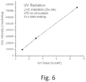
- the material represented by the formula Na 8 Al 6 Si 6 O 24 (Cl,S) 2 was prepared in the following manner: 0.7000 g of dried (500 °C for 1 h) Zeolite A and 0.0600 g of Na 2 SO 4 were mixed. The mixture was heated at 850 °C in air for 48 h. The product was freely cooled down to room temperature and ground. Finally, the product was re-heated at 850 °C for 2 h under a flowing 12 % H 2 + 88 % N 2 atmosphere.
- a sample of the prepared sensor material was then tested.
- a sample of the prepared material was exposed to doses UVC-radiation (254 nm).
- the material was thereafter stored overnight in a dark container.
- the optically stimulated luminescence (OSL) reading was carried out thereafter using a 470 nm stimulation and 10 s data reading time. The results are shown in Fig. 6 .
Landscapes
- Chemical & Material Sciences (AREA)
- General Physics & Mathematics (AREA)
- Physics & Mathematics (AREA)
- Spectroscopy & Molecular Physics (AREA)
- Organic Chemistry (AREA)
- High Energy & Nuclear Physics (AREA)
- Molecular Biology (AREA)
- Life Sciences & Earth Sciences (AREA)
- Health & Medical Sciences (AREA)
- Inorganic Chemistry (AREA)
- Engineering & Computer Science (AREA)
- Materials Engineering (AREA)
- Luminescent Compositions (AREA)
- Photometry And Measurement Of Optical Pulse Characteristics (AREA)
- Investigating, Analyzing Materials By Fluorescence Or Luminescence (AREA)
Claims (27)
- Verfahren zum Bestimmen der Menge eines vorherbestimmten Typs von Strahlung, die auf ein Sensormaterial eingestrahlt wird, wobei das Verfahren umfasst:a) Bereitstellen eines Sensormaterials;b) Aussetzen des Sensormaterials dem vorherbestimmten Typ von Strahlung zum Halten des vorherbestimmten Typs von Strahlung für eine vorherbestimmte Zeitdauer in dem Sensormaterial;c) Unterziehen des Sensormaterials, das dem vorherbestimmten Typ von Strahlung ausgesetzt wurde, einer Wärmebehandlung und/oder einer optischen Anregung; undd) Bestimmen der Menge an sichtbarem Licht, die von dem Sensormaterial emittiert wird, als ein Ergebnis des Unterzogenwerdens der Wärmebehandlung und/oder der optischen Anregung;
dadurch gekennzeichnet, dass das Sensormaterial durch die folgende Formel (I) dargestellt ist:
(M')8(M"M‴)6O24(X,X')2:Mʺʺ Formel (I)
wobeiM' für ein monoatomares Kation eines Alkalimetalls, ausgewählt aus Gruppe 1 des IUPAC-Periodensystems der Elemente, oder eine beliebige Kombination solcher Kationen steht;M" für ein dreiwertiges monoatomares Kation eines Elements, ausgewählt aus Gruppe 13 des IUPAC-Periodensystems der Elemente, oder eines Übergangselements, ausgewählt aus einer beliebigen der Gruppe 3 bis 12 des IUPAC-Periodensystems der Elemente, oder eine beliebige Kombination solcher Kationen steht;M"' für ein monoatomares Kation eines Elements, ausgewählt aus Gruppe 14 des IUPAC-Periodensystems der Elemente, oder eines Elements, ausgewählt aus einer beliebigen der Gruppe 13 und 15 des IUPAC-Periodensystems der Elemente, oder von Zn, oder eine beliebige Kombination solcher Kationen steht;X für ein Anion eines Elements, ausgewählt aus Gruppe 17 des IUPAC-Periodensystems der Elemente, oder eine beliebige Kombination solcher Anionen, oder worin X nicht vorhanden ist, steht;X' für ein Anion eines Elements, ausgewählt aus Gruppe 16 des IUPAC-Periodensystems der Elemente, oder eine beliebige Kombination solcher Anionen, oder worin X nicht vorhanden ist, steht; undM"" für ein Dotierungskation eines Elements, ausgewählt aus Übergangsmetallen des IUPAC-Periodensystems der Elemente, oder eine beliebige Kombination solcher Kationen, oder worin M"" nicht vorhanden ist, steht;unter der Voraussetzung, dass zumindest eines von X und X' vorhanden ist. - Verfahren nach Anspruch 1, wobei der vorherbestimmte Typ von Strahlung elektromagnetische Strahlung ist, aufweisend eine Wellenlänge von über 0 nm bis 590 nm oder über 0 nm bis 560 nm oder über 0 nm bis 500 nm oder über 0 nm bis 400 nm oder über 0 nm bis 300 nm oder 0,000001-590 nm, oder 0,000001-560 nm, oder 0,000001-500 nm, oder 10-590 nm, oder 10-560 nm, oder 10-500 nm, oder 0,000001-400 nm, oder 0,000001-300 nm, oder 0,000001-10 nm, oder 10-400 nm, oder 10-300 nm, oder 0,01-10 nm.
- Verfahren nach einem der Ansprüche 1 bis 2, wobei die Wärmebehandlung Erhöhung der Temperatur des Sensormaterials umfasst.
- Verfahren nach einem der Ansprüche 1 bis 3, wobei die optische Anregung des Sensormaterials Aussetzen des Sensormaterials einer elektromagnetischen Strahlung, aufweisend eine Wellenlänge von 310 bis 1400 nm, umfasst.
- Verfahren nach einem der Ansprüche 1 bis 4, wobei das Verfahren umfasst: e) Vergleichen der bestimmten Menge an Licht, das von dem Sensormaterial emittiert wurde, mit einer Referenz, anzeigend die Korrelation der Menge an emittierten sichtbaren Licht mit der Menge des vorherbestimmten Typs von Strahlung, der das Sensormaterial ausgesetzt wurde.
- Verfahren nach einem der Ansprüche 1 bis 5, wobei M' für ein monoatomares Kation eines Alkalimetalls, ausgewählt aus Gruppe 1 des IUPAC-Periodensystems der Elemente, oder eine beliebige Kombination solcher Kationen, unter der Voraussetzung, dass M' nicht für das monoatomare Kation von Na allein steht, steht.
- Verfahren nach einem der Ansprüche 1 bis 6, wobei M' für eine Kombination von zumindest zwei monoatomaren Kationen verschiedener Alkalimetalle, ausgewählt aus Gruppe 1 des IUPAC-Periodensystems der Elemente, steht.
- Verfahren nach einem der Ansprüche 1 bis 7, wobei M' für eine Kombination von zumindest zwei monoatomaren Kationen verschiedener Alkalimetalle, ausgewählt aus einer Gruppe bestehend aus Li, Na, K und Rb, steht.
- Verfahren nach einem der Ansprüche 1 bis 8, wobei M' für ein monoatomares Kation eines Alkalimetalls, ausgewählt aus der Gruppe bestehend aus Li, K und Rb, oder eine beliebige Kombination solcher Kationen steht.
- Verfahren nach einem der Ansprüche 1 bis 9, wobei M' für eine Kombination aus einem monoatomaren Kation von Na mit einem monoatomaren Kation von Li, einem monoatomaren Kation von K und/oder einem monoatomaren Kation von Rb steht.
- Verfahren nach einem der Ansprüche 1 bis 10, wobei M" für ein dreiwertiges monoatomares Kation eines Metalls, ausgewählt aus einer Gruppe bestehend aus Al und Ga, oder eine Kombination solcher Kationen steht.
- Verfahren nach einem der Ansprüche 1 bis 10, wobei M" für ein dreiwertiges monoatomares Kation von B steht.
- Verfahren nach einem der Ansprüche 1 bis 12, wobei M‴ für ein monoatomares Kation eines Elements, ausgewählt aus einer Gruppe bestehend aus Si und Ge, oder eine Kombination solcher Kationen steht.
- Verfahren nach einem der Ansprüche 1 bis 12, wobei M‴ für ein monoatomares Kation eines Elements, ausgewählt aus einer Gruppe bestehend aus Al, Ga, N, P und As, oder eine beliebige Kombination solcher Kationen steht.
- Verfahren nach einem der Ansprüche 1 bis 14, wobei X für ein Anion eines Elements, ausgewählt aus einer Gruppe bestehend aus F, Cl, Br und I, oder eine beliebige Kombination solcher Anionen steht.
- Verfahren nach einem der Ansprüche 1 bis 15, wobei X' für ein Anion eines Elements, ausgewählt aus einer Gruppe bestehend aus O, S, Se und Te, oder eine beliebige Kombination solcher Anionen steht.
- Verfahren nach einem der Ansprüche 1 bis 16, wobei Mʺʺ für ein Kation eines Elements, ausgewählt aus einer Gruppe bestehend aus Ti, V, Cr, Mn, Fe, Co, Ni, Cu und Zn oder eine beliebige Kombination solcher Kationen steht.
- Erfassungseinrichtung (1) zum Bestimmen der Menge eines vorherbestimmten Typs von Strahlung, die auf ein Sensormaterial eingestrahlt wird, wobei die Erfassungseinrichtung umfasst:- ein Sensormaterial (2), dargestellt durch die Formel (I) wie in einem der Ansprüche 1 bis 17 definiert;- eine Erwärmungseinheit (4), die eingerichtet ist, das Sensormaterial, das dem vorherbestimmten Typ von Strahlung ausgesetzt wurde, einer Wärmebehandlung zu unterziehen, und/oder eine Anregungseinheit (5), die eingerichtet ist, das Sensormaterial, das dem vorherbestimmten Typ von Strahlung ausgesetzt wurde, einer optischen Anregung zu unterziehen; und- eine Messeinheit (6), die eingerichtet ist, die Menge an Licht, die von dem Sensormaterial als ein Ergebnis des Unterzogenwerdens der Wärmebehandlung und/oder der optischen Anregung emittiert wird, zu messen.
- Erfassungseinrichtung nach Anspruch 18, wobei die Erwärmungseinheit (4) eingerichtet ist, die Temperatur des Sensormaterials zu erhöhen.
- Erfassungseinrichtung nach einem der Ansprüche 18 bis 19, wobei die Anregungseinheit (5) eingerichtet ist, das Sensormaterial einer elektromagnetischen Strahlung, aufweisend eine Wellenlänge von 310 bis 1400 nm, auszusetzen.
- Erfassungseinrichtung nach einem der Ansprüche 18 bis 20, wobei die Anregungseinheit (5) ein Laser, eine Leuchtdiode (LED), eine organische Leuchtdiode (OLED), eine organische Aktivmatrix-Leuchtdiode (AMOLED), eine Glühlampe, eine Halogenlampe oder eine Kombination davon ist.
- System (7) zum Bestimmen der Menge eines vorherbestimmten Typs von Strahlung, die auf ein Sensormaterial eingestrahlt wird, wobei das System umfasst:- eine Bestrahlungseinheit (3), die eingerichtet ist, das Sensormaterial dem vorherbestimmten Typ von Strahlung auszusetzen zum Halten des vorherbestimmten Typs von Strahlung in dem Sensormaterial für eine vorherbestimmte Zeitdauer; und- eine Erfassungseinrichtung nach einem der Ansprüche 18 bis 21.
- System nach Anspruch 22, wobei die Bestrahlungseinheit (3) eingerichtet ist, das Sensormaterial elektromagnetischer Strahlung auszusetzen, aufweisend eine Wellenlänge von über 0 nm bis 590 nm, oder über 0 nm bis 560 nm, oder über 0 nm bis 500 nm, oder über 0 nm bis 400 nm, oder über 0 nm bis 300 nm, oder 0,000001-590 nm, oder 0,000001-560 nm, oder 0,000001-500 nm, oder 10-590 nm, oder 10-560 nm, oder 10-500 nm, oder 0,000001-400 nm, oder 0,000001-300 nm, oder 0,000001-10 nm, oder 10-400 nm, oder 10-300 nm, oder 0,01-10 nm.
- System nach einem der Ansprüche 22 bis 23, wobei das System (1) eine Referenz umfasst, die eingerichtet ist, die Korrelation der bestimmten Menge an Licht, die von dem Sensormaterial emittiert wird, mit der Menge des vorherbestimmten Typs von Strahlung, der das Sensormaterial ausgesetzt wurde, anzuzeigen.
- Verwendung einer Wärmebehandlung und/oder einer optischen Anregung zum Bestimmen der Menge eines vorherbestimmten Typs von Strahlung, die auf ein Sensormaterial, dargestellt durch die Formel (I) gemäß einem der Ansprüche 1 bis 17, eingestrahlt wird.
- Verwendung eines Sensormaterials, dargestellt durch die Formel (I), wie in einem der Ansprüche 1 bis 17 definiert, zum Bestimmen der Menge eines vorherbestimmten Typs von Strahlung, die auf das Sensormaterial eingestrahlt wird, wobei das Sensormaterial dem vorherbestimmten Typ von Strahlung ausgesetzt wird zum Halten des vorherbestimmten Typs von Strahlung in dem Sensormaterial für eine vorbestimmte Zeitdauer, und danach einer Wärmebehandlung und/oder einer optischen Anregung unterzogen wird.
- Verwendung eines Sensormaterials, dargestellt durch die Formel (I), wie in einem der Ansprüche 1 bis 17 definiert, in einem Thermolumineszenz-Dosimeter oder in einem optisch angeregten Lumineszenz-Dosimeter.
Applications Claiming Priority (2)
| Application Number | Priority Date | Filing Date | Title |
|---|---|---|---|
| FI20175992A FI20175992A1 (en) | 2017-11-07 | 2017-11-07 | Determination of the amount of radiation of a predetermined type irradiated on a sensor material |
| PCT/FI2018/050761 WO2019092308A1 (en) | 2017-11-07 | 2018-10-17 | Determining the amount of a predetermined type of radiation irradiated on a sensor material |
Publications (2)
| Publication Number | Publication Date |
|---|---|
| EP3707533A1 EP3707533A1 (de) | 2020-09-16 |
| EP3707533B1 true EP3707533B1 (de) | 2021-12-01 |
Family
ID=64051604
Family Applications (1)
| Application Number | Title | Priority Date | Filing Date |
|---|---|---|---|
| EP18796081.0A Active EP3707533B1 (de) | 2017-11-07 | 2018-10-17 | Bestimmung der menge eines vorbestimmten, auf ein sensormaterial gestrahlten strahlungstyps |
Country Status (11)
| Country | Link |
|---|---|
| US (1) | US11079498B2 (de) |
| EP (1) | EP3707533B1 (de) |
| JP (1) | JP7003250B2 (de) |
| KR (1) | KR20200081414A (de) |
| CN (1) | CN111316131B (de) |
| AU (1) | AU2018363225A1 (de) |
| BR (1) | BR112020008961A2 (de) |
| CA (1) | CA3081148A1 (de) |
| FI (1) | FI20175992A1 (de) |
| TW (1) | TW201928399A (de) |
| WO (1) | WO2019092308A1 (de) |
Families Citing this family (6)
| Publication number | Priority date | Publication date | Assignee | Title |
|---|---|---|---|---|
| FI129159B (en) * | 2017-11-07 | 2021-08-13 | Turun Yliopisto | Indicating the intensity of a predetermined type of radiation |
| FI130418B (en) | 2021-05-05 | 2023-08-21 | Turun Yliopisto | Procedure for heat treatment of luminescent materials |
| FI130417B (en) | 2021-05-05 | 2023-08-21 | Turun Yliopisto | Procedure for electron bombardment of luminescent materials |
| TW202314236A (zh) * | 2021-07-27 | 2023-04-01 | 圖爾庫大學 | 輻射量決定方法及其用途、創建輻射圖的方法以及劑量計 |
| WO2024028538A1 (en) * | 2022-08-05 | 2024-02-08 | Turun Yliopisto | A method for determining exposure to nuclear radiation |
| US20250003878A1 (en) * | 2023-04-12 | 2025-01-02 | Sunrez Corporation | Validation of degree of cure with uv radiation by means of fluorescing with exposure to uv light |
Family Cites Families (12)
| Publication number | Priority date | Publication date | Assignee | Title |
|---|---|---|---|---|
| FR2209717B1 (de) | 1972-12-12 | 1976-11-19 | Ibm | |
| DE3144422C2 (de) * | 1980-04-15 | 1985-07-04 | Institut fiziki Akademii Nauk Estonskoj SSR, Tartu | Foto- und kathodochromer Sodalith und dessen Verwendung |
| US5656815A (en) * | 1996-02-08 | 1997-08-12 | The United States Of America As Represented By The Secretary Of The Navy | Thermoluminescence radiation dosimetry using transparent glass containing nanocrystalline phosphor |
| DE19833176C2 (de) | 1998-07-23 | 2001-02-01 | Georg Gebhard | Vorrichtung zur Messung und Anzeige von UV-Strahlung |
| GB0427407D0 (en) | 2004-12-14 | 2005-01-19 | Rue De Int Ltd | Security material |
| WO2006063409A1 (en) * | 2004-12-17 | 2006-06-22 | Newsouth Innovations Pty Limited | Radiation storage phosphor & applications |
| US20100176343A1 (en) | 2005-02-02 | 2010-07-15 | Wei Chen | Energy-transfer nanocomposite materials and methods of making and using same |
| US8633455B2 (en) * | 2010-01-12 | 2014-01-21 | Landauer, Inc. | Optical system for dosimeter reader |
| JP5792612B2 (ja) * | 2011-12-27 | 2015-10-14 | 株式会社日立製作所 | 放射線強度計測装置 |
| EP2945997B1 (de) * | 2013-01-15 | 2016-10-05 | Merck Patent GmbH | Leuchtstoffe auf der basis von alumosilikaten |
| US9121948B2 (en) * | 2013-03-12 | 2015-09-01 | The United States Of America, As Represented By The Secretary Of The Navy | Optically stimulated luminescence dosimetry using doped lithium fluoride crystals |
| JP6420637B2 (ja) | 2014-11-20 | 2018-11-07 | 日立Geニュークリア・エナジー株式会社 | 放射線計測装置及びその計測方法 |
-
2017
- 2017-11-07 FI FI20175992A patent/FI20175992A1/en not_active IP Right Cessation
-
2018
- 2018-10-17 WO PCT/FI2018/050761 patent/WO2019092308A1/en not_active Ceased
- 2018-10-17 AU AU2018363225A patent/AU2018363225A1/en not_active Abandoned
- 2018-10-17 CA CA3081148A patent/CA3081148A1/en active Pending
- 2018-10-17 JP JP2020523249A patent/JP7003250B2/ja not_active Expired - Fee Related
- 2018-10-17 KR KR1020207014707A patent/KR20200081414A/ko not_active Ceased
- 2018-10-17 BR BR112020008961-3A patent/BR112020008961A2/pt not_active IP Right Cessation
- 2018-10-17 US US16/761,952 patent/US11079498B2/en not_active Expired - Fee Related
- 2018-10-17 EP EP18796081.0A patent/EP3707533B1/de active Active
- 2018-10-17 CN CN201880071669.6A patent/CN111316131B/zh not_active Expired - Fee Related
- 2018-11-07 TW TW107139498A patent/TW201928399A/zh unknown
Also Published As
| Publication number | Publication date |
|---|---|
| RU2020116409A3 (de) | 2022-03-04 |
| KR20200081414A (ko) | 2020-07-07 |
| FI20175992A1 (en) | 2019-05-08 |
| WO2019092308A1 (en) | 2019-05-16 |
| EP3707533A1 (de) | 2020-09-16 |
| TW201928399A (zh) | 2019-07-16 |
| AU2018363225A1 (en) | 2020-05-28 |
| BR112020008961A2 (pt) | 2020-10-20 |
| CA3081148A1 (en) | 2019-05-16 |
| CN111316131B (zh) | 2021-07-02 |
| CN111316131A (zh) | 2020-06-19 |
| JP2021501881A (ja) | 2021-01-21 |
| US20200386899A1 (en) | 2020-12-10 |
| US11079498B2 (en) | 2021-08-03 |
| JP7003250B2 (ja) | 2022-01-20 |
| RU2020116409A (ru) | 2021-12-08 |
Similar Documents
| Publication | Publication Date | Title |
|---|---|---|
| US11079498B2 (en) | Determining the amount of a predetermined type of radiation irradiated on a sensor material | |
| Yang et al. | Passive dosimeters for radiation dosimetry: materials, mechanisms, and applications | |
| Gai et al. | Synthesis of LiMgPO4: Eu, Sm, B phosphors and investigation of their optically stimulated luminescence properties | |
| US10533131B2 (en) | Synthetic material for detecting ultraviolet radiation and/or X-radiation | |
| Ekendahl et al. | OSL and TL retrospective dosimetry with a fluorapatite glass-ceramic used for dental restorations | |
| Ekendahl et al. | A low-cost personal dosemeter based on optically stimulated luminescence (OSL) of common household salt (NaCl) | |
| Malthez et al. | Experimental photon energy response of different dosimetric materials for a dual detector system combining thermoluminescence and optically stimulated luminescence | |
| Chopra et al. | Thermoluminescent study of borates for dosimetric applications | |
| US20240318075A1 (en) | A radiation sensing material | |
| Kouroukla | Luminescence dosimetry with ceramic materials for application to radiological emergencies and other incidents. | |
| RU2773276C2 (ru) | Определение количества излучения заранее заданного типа, облучившего материал датчика | |
| US10941340B2 (en) | Synthetic material for detecting ultraviolet radiation and/or X-radiation | |
| Mahala et al. | Study of radiophotoluminescence of Eu doped CaSO4 phosphor for gamma dosimetric applications |
Legal Events
| Date | Code | Title | Description |
|---|---|---|---|
| STAA | Information on the status of an ep patent application or granted ep patent |
Free format text: STATUS: UNKNOWN |
|
| STAA | Information on the status of an ep patent application or granted ep patent |
Free format text: STATUS: THE INTERNATIONAL PUBLICATION HAS BEEN MADE |
|
| PUAI | Public reference made under article 153(3) epc to a published international application that has entered the european phase |
Free format text: ORIGINAL CODE: 0009012 |
|
| STAA | Information on the status of an ep patent application or granted ep patent |
Free format text: STATUS: REQUEST FOR EXAMINATION WAS MADE |
|
| 17P | Request for examination filed |
Effective date: 20200421 |
|
| AK | Designated contracting states |
Kind code of ref document: A1 Designated state(s): AL AT BE BG CH CY CZ DE DK EE ES FI FR GB GR HR HU IE IS IT LI LT LU LV MC MK MT NL NO PL PT RO RS SE SI SK SM TR |
|
| AX | Request for extension of the european patent |
Extension state: BA ME |
|
| DAV | Request for validation of the european patent (deleted) | ||
| DAX | Request for extension of the european patent (deleted) | ||
| GRAP | Despatch of communication of intention to grant a patent |
Free format text: ORIGINAL CODE: EPIDOSNIGR1 |
|
| STAA | Information on the status of an ep patent application or granted ep patent |
Free format text: STATUS: GRANT OF PATENT IS INTENDED |
|
| INTG | Intention to grant announced |
Effective date: 20210706 |
|
| GRAS | Grant fee paid |
Free format text: ORIGINAL CODE: EPIDOSNIGR3 |
|
| GRAA | (expected) grant |
Free format text: ORIGINAL CODE: 0009210 |
|
| STAA | Information on the status of an ep patent application or granted ep patent |
Free format text: STATUS: THE PATENT HAS BEEN GRANTED |
|
| RIN1 | Information on inventor provided before grant (corrected) |
Inventor name: NORRBO, ISABELLA Inventor name: LASTUSAARI, MIKA |
|
| AK | Designated contracting states |
Kind code of ref document: B1 Designated state(s): AL AT BE BG CH CY CZ DE DK EE ES FI FR GB GR HR HU IE IS IT LI LT LU LV MC MK MT NL NO PL PT RO RS SE SI SK SM TR |
|
| REG | Reference to a national code |
Ref country code: GB Ref legal event code: FG4D |
|
| REG | Reference to a national code |
Ref country code: AT Ref legal event code: REF Ref document number: 1452304 Country of ref document: AT Kind code of ref document: T Effective date: 20211215 Ref country code: CH Ref legal event code: EP |
|
| REG | Reference to a national code |
Ref country code: IE Ref legal event code: FG4D |
|
| REG | Reference to a national code |
Ref country code: DE Ref legal event code: R096 Ref document number: 602018027612 Country of ref document: DE |
|
| REG | Reference to a national code |
Ref country code: FI Ref legal event code: FGE |
|
| REG | Reference to a national code |
Ref country code: DE Ref legal event code: R081 Ref document number: 602018027612 Country of ref document: DE Owner name: PURE LUMINESCENCE TECHNOLOGIES OY, FI Free format text: FORMER OWNER: TURUN YLIOPISTO, TURUN YLIOPISTO, FI |
|
| REG | Reference to a national code |
Ref country code: SE Ref legal event code: TRGR |
|
| REG | Reference to a national code |
Ref country code: LT Ref legal event code: MG9D |
|
| RAP2 | Party data changed (patent owner data changed or rights of a patent transferred) |
Owner name: PURE LUMINESCENCE TECNOLOGIES OY |
|
| REG | Reference to a national code |
Ref country code: NL Ref legal event code: MP Effective date: 20211201 |
|
| REG | Reference to a national code |
Ref country code: AT Ref legal event code: MK05 Ref document number: 1452304 Country of ref document: AT Kind code of ref document: T Effective date: 20211201 |
|
| REG | Reference to a national code |
Ref country code: BE Ref legal event code: PD Owner name: PURE LUMINESCENCE TECHNOLOGIES OY; FI Free format text: DETAILS ASSIGNMENT: CHANGE OF OWNER(S), ASSIGNMENT; FORMER OWNER NAME: TURUN YLIOPISTO Effective date: 20220225 |
|
| PG25 | Lapsed in a contracting state [announced via postgrant information from national office to epo] |
Ref country code: RS Free format text: LAPSE BECAUSE OF FAILURE TO SUBMIT A TRANSLATION OF THE DESCRIPTION OR TO PAY THE FEE WITHIN THE PRESCRIBED TIME-LIMIT Effective date: 20211201 Ref country code: LT Free format text: LAPSE BECAUSE OF FAILURE TO SUBMIT A TRANSLATION OF THE DESCRIPTION OR TO PAY THE FEE WITHIN THE PRESCRIBED TIME-LIMIT Effective date: 20211201 Ref country code: BG Free format text: LAPSE BECAUSE OF FAILURE TO SUBMIT A TRANSLATION OF THE DESCRIPTION OR TO PAY THE FEE WITHIN THE PRESCRIBED TIME-LIMIT Effective date: 20220301 Ref country code: AT Free format text: LAPSE BECAUSE OF FAILURE TO SUBMIT A TRANSLATION OF THE DESCRIPTION OR TO PAY THE FEE WITHIN THE PRESCRIBED TIME-LIMIT Effective date: 20211201 |
|
| PG25 | Lapsed in a contracting state [announced via postgrant information from national office to epo] |
Ref country code: PL Free format text: LAPSE BECAUSE OF FAILURE TO SUBMIT A TRANSLATION OF THE DESCRIPTION OR TO PAY THE FEE WITHIN THE PRESCRIBED TIME-LIMIT Effective date: 20211201 Ref country code: NO Free format text: LAPSE BECAUSE OF FAILURE TO SUBMIT A TRANSLATION OF THE DESCRIPTION OR TO PAY THE FEE WITHIN THE PRESCRIBED TIME-LIMIT Effective date: 20220301 Ref country code: LV Free format text: LAPSE BECAUSE OF FAILURE TO SUBMIT A TRANSLATION OF THE DESCRIPTION OR TO PAY THE FEE WITHIN THE PRESCRIBED TIME-LIMIT Effective date: 20211201 Ref country code: HR Free format text: LAPSE BECAUSE OF FAILURE TO SUBMIT A TRANSLATION OF THE DESCRIPTION OR TO PAY THE FEE WITHIN THE PRESCRIBED TIME-LIMIT Effective date: 20211201 Ref country code: GR Free format text: LAPSE BECAUSE OF FAILURE TO SUBMIT A TRANSLATION OF THE DESCRIPTION OR TO PAY THE FEE WITHIN THE PRESCRIBED TIME-LIMIT Effective date: 20220302 |
|
| REG | Reference to a national code |
Ref country code: GB Ref legal event code: 732E Free format text: REGISTERED BETWEEN 20220513 AND 20220518 |
|
| PG25 | Lapsed in a contracting state [announced via postgrant information from national office to epo] |
Ref country code: NL Free format text: LAPSE BECAUSE OF FAILURE TO SUBMIT A TRANSLATION OF THE DESCRIPTION OR TO PAY THE FEE WITHIN THE PRESCRIBED TIME-LIMIT Effective date: 20211201 |
|
| PG25 | Lapsed in a contracting state [announced via postgrant information from national office to epo] |
Ref country code: SM Free format text: LAPSE BECAUSE OF FAILURE TO SUBMIT A TRANSLATION OF THE DESCRIPTION OR TO PAY THE FEE WITHIN THE PRESCRIBED TIME-LIMIT Effective date: 20211201 Ref country code: SK Free format text: LAPSE BECAUSE OF FAILURE TO SUBMIT A TRANSLATION OF THE DESCRIPTION OR TO PAY THE FEE WITHIN THE PRESCRIBED TIME-LIMIT Effective date: 20211201 Ref country code: RO Free format text: LAPSE BECAUSE OF FAILURE TO SUBMIT A TRANSLATION OF THE DESCRIPTION OR TO PAY THE FEE WITHIN THE PRESCRIBED TIME-LIMIT Effective date: 20211201 Ref country code: PT Free format text: LAPSE BECAUSE OF FAILURE TO SUBMIT A TRANSLATION OF THE DESCRIPTION OR TO PAY THE FEE WITHIN THE PRESCRIBED TIME-LIMIT Effective date: 20220401 Ref country code: ES Free format text: LAPSE BECAUSE OF FAILURE TO SUBMIT A TRANSLATION OF THE DESCRIPTION OR TO PAY THE FEE WITHIN THE PRESCRIBED TIME-LIMIT Effective date: 20211201 Ref country code: EE Free format text: LAPSE BECAUSE OF FAILURE TO SUBMIT A TRANSLATION OF THE DESCRIPTION OR TO PAY THE FEE WITHIN THE PRESCRIBED TIME-LIMIT Effective date: 20211201 Ref country code: CZ Free format text: LAPSE BECAUSE OF FAILURE TO SUBMIT A TRANSLATION OF THE DESCRIPTION OR TO PAY THE FEE WITHIN THE PRESCRIBED TIME-LIMIT Effective date: 20211201 |
|
| REG | Reference to a national code |
Ref country code: DE Ref legal event code: R097 Ref document number: 602018027612 Country of ref document: DE |
|
| PG25 | Lapsed in a contracting state [announced via postgrant information from national office to epo] |
Ref country code: IS Free format text: LAPSE BECAUSE OF FAILURE TO SUBMIT A TRANSLATION OF THE DESCRIPTION OR TO PAY THE FEE WITHIN THE PRESCRIBED TIME-LIMIT Effective date: 20220401 |
|
| PLBE | No opposition filed within time limit |
Free format text: ORIGINAL CODE: 0009261 |
|
| STAA | Information on the status of an ep patent application or granted ep patent |
Free format text: STATUS: NO OPPOSITION FILED WITHIN TIME LIMIT |
|
| PG25 | Lapsed in a contracting state [announced via postgrant information from national office to epo] |
Ref country code: DK Free format text: LAPSE BECAUSE OF FAILURE TO SUBMIT A TRANSLATION OF THE DESCRIPTION OR TO PAY THE FEE WITHIN THE PRESCRIBED TIME-LIMIT Effective date: 20211201 Ref country code: AL Free format text: LAPSE BECAUSE OF FAILURE TO SUBMIT A TRANSLATION OF THE DESCRIPTION OR TO PAY THE FEE WITHIN THE PRESCRIBED TIME-LIMIT Effective date: 20211201 |
|
| RAP4 | Party data changed (patent owner data changed or rights of a patent transferred) |
Owner name: PURE LUMINESCENCE TECHNOLOGIES OY |
|
| 26N | No opposition filed |
Effective date: 20220902 |
|
| PG25 | Lapsed in a contracting state [announced via postgrant information from national office to epo] |
Ref country code: SI Free format text: LAPSE BECAUSE OF FAILURE TO SUBMIT A TRANSLATION OF THE DESCRIPTION OR TO PAY THE FEE WITHIN THE PRESCRIBED TIME-LIMIT Effective date: 20211201 |
|
| PG25 | Lapsed in a contracting state [announced via postgrant information from national office to epo] |
Ref country code: MC Free format text: LAPSE BECAUSE OF FAILURE TO SUBMIT A TRANSLATION OF THE DESCRIPTION OR TO PAY THE FEE WITHIN THE PRESCRIBED TIME-LIMIT Effective date: 20211201 |
|
| PG25 | Lapsed in a contracting state [announced via postgrant information from national office to epo] |
Ref country code: LU Free format text: LAPSE BECAUSE OF NON-PAYMENT OF DUE FEES Effective date: 20221017 |
|
| P01 | Opt-out of the competence of the unified patent court (upc) registered |
Effective date: 20230526 |
|
| PG25 | Lapsed in a contracting state [announced via postgrant information from national office to epo] |
Ref country code: IE Free format text: LAPSE BECAUSE OF NON-PAYMENT OF DUE FEES Effective date: 20221017 |
|
| PGFP | Annual fee paid to national office [announced via postgrant information from national office to epo] |
Ref country code: GB Payment date: 20231018 Year of fee payment: 6 |
|
| PGFP | Annual fee paid to national office [announced via postgrant information from national office to epo] |
Ref country code: SE Payment date: 20231017 Year of fee payment: 6 Ref country code: IT Payment date: 20231023 Year of fee payment: 6 Ref country code: FR Payment date: 20231016 Year of fee payment: 6 Ref country code: FI Payment date: 20231017 Year of fee payment: 6 Ref country code: DE Payment date: 20231020 Year of fee payment: 6 Ref country code: CH Payment date: 20231102 Year of fee payment: 6 |
|
| PGFP | Annual fee paid to national office [announced via postgrant information from national office to epo] |
Ref country code: BE Payment date: 20231016 Year of fee payment: 6 |
|
| PG25 | Lapsed in a contracting state [announced via postgrant information from national office to epo] |
Ref country code: CY Free format text: LAPSE BECAUSE OF FAILURE TO SUBMIT A TRANSLATION OF THE DESCRIPTION OR TO PAY THE FEE WITHIN THE PRESCRIBED TIME-LIMIT Effective date: 20211201 |
|
| PG25 | Lapsed in a contracting state [announced via postgrant information from national office to epo] |
Ref country code: MK Free format text: LAPSE BECAUSE OF FAILURE TO SUBMIT A TRANSLATION OF THE DESCRIPTION OR TO PAY THE FEE WITHIN THE PRESCRIBED TIME-LIMIT Effective date: 20211201 Ref country code: HU Free format text: LAPSE BECAUSE OF FAILURE TO SUBMIT A TRANSLATION OF THE DESCRIPTION OR TO PAY THE FEE WITHIN THE PRESCRIBED TIME-LIMIT; INVALID AB INITIO Effective date: 20181017 |
|
| PG25 | Lapsed in a contracting state [announced via postgrant information from national office to epo] |
Ref country code: TR Free format text: LAPSE BECAUSE OF FAILURE TO SUBMIT A TRANSLATION OF THE DESCRIPTION OR TO PAY THE FEE WITHIN THE PRESCRIBED TIME-LIMIT Effective date: 20211201 |
|
| PG25 | Lapsed in a contracting state [announced via postgrant information from national office to epo] |
Ref country code: MT Free format text: LAPSE BECAUSE OF FAILURE TO SUBMIT A TRANSLATION OF THE DESCRIPTION OR TO PAY THE FEE WITHIN THE PRESCRIBED TIME-LIMIT Effective date: 20211201 |
|
| REG | Reference to a national code |
Ref country code: DE Ref legal event code: R119 Ref document number: 602018027612 Country of ref document: DE |
|
| REG | Reference to a national code |
Ref country code: CH Ref legal event code: PL |
|
| REG | Reference to a national code |
Ref country code: SE Ref legal event code: EUG |
|
| GBPC | Gb: european patent ceased through non-payment of renewal fee |
Effective date: 20241017 |
|
| PG25 | Lapsed in a contracting state [announced via postgrant information from national office to epo] |
Ref country code: FI Free format text: LAPSE BECAUSE OF NON-PAYMENT OF DUE FEES Effective date: 20241017 |
|
| PG25 | Lapsed in a contracting state [announced via postgrant information from national office to epo] |
Ref country code: DE Free format text: LAPSE BECAUSE OF NON-PAYMENT OF DUE FEES Effective date: 20250501 |
|
| PG25 | Lapsed in a contracting state [announced via postgrant information from national office to epo] |
Ref country code: GB Free format text: LAPSE BECAUSE OF NON-PAYMENT OF DUE FEES Effective date: 20241017 |
|
| PG25 | Lapsed in a contracting state [announced via postgrant information from national office to epo] |
Ref country code: BE Free format text: LAPSE BECAUSE OF NON-PAYMENT OF DUE FEES Effective date: 20241031 |
|
| PG25 | Lapsed in a contracting state [announced via postgrant information from national office to epo] |
Ref country code: FR Free format text: LAPSE BECAUSE OF NON-PAYMENT OF DUE FEES Effective date: 20241031 |
|
| PG25 | Lapsed in a contracting state [announced via postgrant information from national office to epo] |
Ref country code: CH Free format text: LAPSE BECAUSE OF NON-PAYMENT OF DUE FEES Effective date: 20241031 |
|
| REG | Reference to a national code |
Ref country code: BE Ref legal event code: MM Effective date: 20241031 |
|
| PG25 | Lapsed in a contracting state [announced via postgrant information from national office to epo] |
Ref country code: SE Free format text: LAPSE BECAUSE OF NON-PAYMENT OF DUE FEES Effective date: 20241018 Ref country code: IT Free format text: LAPSE BECAUSE OF NON-PAYMENT OF DUE FEES Effective date: 20241017 |