EP3706286A1 - Power reception device and non-contact power transmission system - Google Patents
Power reception device and non-contact power transmission system Download PDFInfo
- Publication number
- EP3706286A1 EP3706286A1 EP17930775.6A EP17930775A EP3706286A1 EP 3706286 A1 EP3706286 A1 EP 3706286A1 EP 17930775 A EP17930775 A EP 17930775A EP 3706286 A1 EP3706286 A1 EP 3706286A1
- Authority
- EP
- European Patent Office
- Prior art keywords
- power reception
- power
- coil
- circuit
- reception coil
- Prior art date
- Legal status (The legal status is an assumption and is not a legal conclusion. Google has not performed a legal analysis and makes no representation as to the accuracy of the status listed.)
- Granted
Links
- 230000005540 biological transmission Effects 0.000 title claims description 121
- 239000000758 substrate Substances 0.000 claims abstract description 69
- 239000004065 semiconductor Substances 0.000 claims description 14
- 238000006243 chemical reaction Methods 0.000 claims description 12
- 229910002601 GaN Inorganic materials 0.000 claims description 4
- JMASRVWKEDWRBT-UHFFFAOYSA-N Gallium nitride Chemical compound [Ga]#N JMASRVWKEDWRBT-UHFFFAOYSA-N 0.000 claims description 4
- 239000010432 diamond Substances 0.000 claims description 2
- 229910003460 diamond Inorganic materials 0.000 claims description 2
- 239000000463 material Substances 0.000 claims description 2
- HBMJWWWQQXIZIP-UHFFFAOYSA-N silicon carbide Chemical group [Si+]#[C-] HBMJWWWQQXIZIP-UHFFFAOYSA-N 0.000 claims description 2
- 229910010271 silicon carbide Inorganic materials 0.000 claims description 2
- 238000010586 diagram Methods 0.000 description 19
- 230000005674 electromagnetic induction Effects 0.000 description 9
- 238000000034 method Methods 0.000 description 7
- 238000001646 magnetic resonance method Methods 0.000 description 6
- 239000003990 capacitor Substances 0.000 description 5
- 230000008878 coupling Effects 0.000 description 4
- 238000010168 coupling process Methods 0.000 description 4
- 238000005859 coupling reaction Methods 0.000 description 4
- 230000004907 flux Effects 0.000 description 4
- RYGMFSIKBFXOCR-UHFFFAOYSA-N Copper Chemical compound [Cu] RYGMFSIKBFXOCR-UHFFFAOYSA-N 0.000 description 3
- 239000011889 copper foil Substances 0.000 description 3
- 230000004048 modification Effects 0.000 description 3
- 238000012986 modification Methods 0.000 description 3
- 230000008901 benefit Effects 0.000 description 2
- 230000001413 cellular effect Effects 0.000 description 2
- 230000005672 electromagnetic field Effects 0.000 description 2
- 230000007257 malfunction Effects 0.000 description 2
- 230000007246 mechanism Effects 0.000 description 2
- 230000002093 peripheral effect Effects 0.000 description 2
- 230000005855 radiation Effects 0.000 description 2
- 238000009774 resonance method Methods 0.000 description 2
- 238000004804 winding Methods 0.000 description 2
- 230000002596 correlated effect Effects 0.000 description 1
- 230000000694 effects Effects 0.000 description 1
- 238000009499 grossing Methods 0.000 description 1
- 230000017525 heat dissipation Effects 0.000 description 1
- 239000004973 liquid crystal related substance Substances 0.000 description 1
- 238000004519 manufacturing process Methods 0.000 description 1
- 239000002184 metal Substances 0.000 description 1
- 229910052751 metal Inorganic materials 0.000 description 1
- 229910052710 silicon Inorganic materials 0.000 description 1
- 239000010703 silicon Substances 0.000 description 1
Images


Classifications
-
- H—ELECTRICITY
- H02—GENERATION; CONVERSION OR DISTRIBUTION OF ELECTRIC POWER
- H02J—CIRCUIT ARRANGEMENTS OR SYSTEMS FOR SUPPLYING OR DISTRIBUTING ELECTRIC POWER; SYSTEMS FOR STORING ELECTRIC ENERGY
- H02J50/00—Circuit arrangements or systems for wireless supply or distribution of electric power
- H02J50/10—Circuit arrangements or systems for wireless supply or distribution of electric power using inductive coupling
- H02J50/12—Circuit arrangements or systems for wireless supply or distribution of electric power using inductive coupling of the resonant type
-
- H—ELECTRICITY
- H02—GENERATION; CONVERSION OR DISTRIBUTION OF ELECTRIC POWER
- H02J—CIRCUIT ARRANGEMENTS OR SYSTEMS FOR SUPPLYING OR DISTRIBUTING ELECTRIC POWER; SYSTEMS FOR STORING ELECTRIC ENERGY
- H02J50/00—Circuit arrangements or systems for wireless supply or distribution of electric power
- H02J50/005—Mechanical details of housing or structure aiming to accommodate the power transfer means, e.g. mechanical integration of coils, antennas or transducers into emitting or receiving devices
-
- H—ELECTRICITY
- H02—GENERATION; CONVERSION OR DISTRIBUTION OF ELECTRIC POWER
- H02J—CIRCUIT ARRANGEMENTS OR SYSTEMS FOR SUPPLYING OR DISTRIBUTING ELECTRIC POWER; SYSTEMS FOR STORING ELECTRIC ENERGY
- H02J50/00—Circuit arrangements or systems for wireless supply or distribution of electric power
- H02J50/40—Circuit arrangements or systems for wireless supply or distribution of electric power using two or more transmitting or receiving devices
- H02J50/402—Circuit arrangements or systems for wireless supply or distribution of electric power using two or more transmitting or receiving devices the two or more transmitting or the two or more receiving devices being integrated in the same unit, e.g. power mats with several coils or antennas with several sub-antennas
-
- H—ELECTRICITY
- H02—GENERATION; CONVERSION OR DISTRIBUTION OF ELECTRIC POWER
- H02J—CIRCUIT ARRANGEMENTS OR SYSTEMS FOR SUPPLYING OR DISTRIBUTING ELECTRIC POWER; SYSTEMS FOR STORING ELECTRIC ENERGY
- H02J50/00—Circuit arrangements or systems for wireless supply or distribution of electric power
- H02J50/70—Circuit arrangements or systems for wireless supply or distribution of electric power involving the reduction of electric, magnetic or electromagnetic leakage fields
-
- H—ELECTRICITY
- H02—GENERATION; CONVERSION OR DISTRIBUTION OF ELECTRIC POWER
- H02J—CIRCUIT ARRANGEMENTS OR SYSTEMS FOR SUPPLYING OR DISTRIBUTING ELECTRIC POWER; SYSTEMS FOR STORING ELECTRIC ENERGY
- H02J50/00—Circuit arrangements or systems for wireless supply or distribution of electric power
- H02J50/90—Circuit arrangements or systems for wireless supply or distribution of electric power involving detection or optimisation of position, e.g. alignment
-
- H—ELECTRICITY
- H04—ELECTRIC COMMUNICATION TECHNIQUE
- H04B—TRANSMISSION
- H04B5/00—Near-field transmission systems, e.g. inductive or capacitive transmission systems
- H04B5/70—Near-field transmission systems, e.g. inductive or capacitive transmission systems specially adapted for specific purposes
- H04B5/79—Near-field transmission systems, e.g. inductive or capacitive transmission systems specially adapted for specific purposes for data transfer in combination with power transfer
Definitions
- the present disclosure relates to a power reception device that receives power in a contactless manner and according to a magnetic resonance method, and a contactless power transmission system including the power reception device.
- a cellular phone including the following power reception coil and circuit board.
- the power reception coil receives power transferred from a power transmission coil using electromagnetic induction, and on the circuit board, a conversion circuit is mounted to convert alternating current induced in the power reception coil into direct current and output the direct current (see, for example, Patent Literature 1).
- This cellular phone includes a movable case that houses the power reception coil and a main-body case that houses the circuit board, and the movable case and the main-body case are provided as separate cases.
- the movable case is coupled to the main-body case such that the power reception coil can be separated from the circuit board.
- a wireless power transmission system which transmits power using magnetic field resonance between a power transmission coil and a power reception coil (see, for example, Patent Literature 2).
- a magnetic field resonance method a power transmission device and a power reception device are provided with respective resonance circuits each employing a coil and a capacitor, and the resonance frequencies of these resonance circuits are made to coincide with each other, whereby power is transmitted from the power transmission device to the power reception device.
- wireless power transmission by the magnetic field resonance method it is possible to transmit power with a high efficiency even if the power transmission device and the power reception device are separated from each other to a certain extent.
- the magnetic field resonance is also referred to as magnetic resonance.
- the movable case that houses the power reception coil is provided apart from the circuit board, thereby preventing the circuit board from malfunctioning because of electromagnetic wave noise of the power transmission coil.
- the distance between the power transmission coil and the power reception coil needs to be short, as compared with the power transmission by the magnetic resonance method, and the position of the power reception device is restricted.
- the distance between the power transmission coil and the power reception coil can be set great, as compared with the power transmission by the electromagnetic induction method, and the restriction on the position of the power reception device can be reduced.
- the frequency of power transmitted by magnetic resonance is higher than that of power transmitted by electromagnetic induction.
- the frequency of power transmitted by electromagnetic induction is in the kHz band, whereas the resonance frequency of magnetic resonance is in the MHz band.
- a loss caused by an inductance of a wire such as a lead connecting a power reception coil housed in a movable case and a circuit board (power reception circuit) housed in a main-body case is increased. Furthermore, a high-frequency noise is made in the wire such as the lead connecting the power reception coil and the circuit board, and causes the circuit board to malfunction.
- the present disclosure is applied to solve the above problems, and relates to a power reception device and a contactless power transmission system that can reduce a power loss and a high-frequency noise between a power reception coil that receives power through magnetic resonance and a power reception circuit.
- a power reception device includes: a power reception coil that receives power by magnetic resonance; a power reception circuit that converts power received by the power reception coil into direct current; a load circuit that operates by the directed current into which the power is converted by the power reception circuit; a first substrate on which the power reception coil and the power reception circuit are mounted; and a second substrate on which the load circuit is mounted, the second substrate being located outside the power reception coil as viewed in an axial direction of the power reception coil.
- the power reception coil and the power reception circuit are mounted on the first substrate. Therefore, the inductance of a connection path between the power reception coil and the power reception circuit can be reduced to a small value, and a power loss and a high-frequency noise can be reduced, as compared with the case where the power reception circuit is mounted on the second substrate, which is provided separate from the first substrate.
- Fig. 1 is a plan view schematically illustrating an internal configuration of a power reception device according to Embodiment 1.
- Fig. 2 is a diagram schematically illustrating a cross section taken along line A-A in Fig. 1 .
- a power reception device 100 includes a first substrate 10 and a second substrate 20 both housed in a housing 1.
- a power reception coil 30 and a power reception circuit 40 are mounted on the first substrate 10.
- the power reception coil 30 receives power through magnetic resonance.
- the power reception coil 30 is a flat coil in which a wiring pattern such as copper foil is spirally formed. It should be noted that the power reception coil 30 is not limited to the wiring pattern, and may be formed by spirally winding an arbitrary conductive line and may be mounted on the first substrate 10. Furthermore, the power reception coil 30 may be formed to have a plurality of layers stacked.
- a cutout portion 11 which is a through hole extending through the first substrate 10, is formed. It should be noted that it is not indispensable that the cutout portion 11 is formed; that is, no cutout portion 11 may be provided.
- the power reception circuit 40 converts power received by the power reception coil 30 into direct current. A detailed configuration of the circuit configuration will be described later.
- the power reception coil 30 and the power reception circuit 40 are connected by a wiring pattern formed on the first substrate 10.
- the positions of the power reception coil 30 and the power reception circuit 40 on the first substrate 10 will be described with reference to Fig. 3 .
- Fig. 3 is a plan view for explaining the positions of the power reception coil and the power reception circuit of the power reception device according to Embodiment 1.
- a first region 12 and a second region 13 are adjacent to each other as viewed in a direction along an axis AX of the power reception coil 30; and in the first region 12, the power reception coil 30 is provided, and in the second region 13, the power reception circuit 40 is provided. That is, the power reception coil 30 and the power reception circuit 40 are provided on the first substrate 10 such that the wiring pattern connecting the power reception coil 30 and the power reception circuit 40 is set to have the shortest possible length.
- a load circuit 50 is mounted on the second substrate 20 .
- the load circuit 50 is operated by the direct current obtained by conversion performed by the power reception circuit 40.
- the load circuit 50 and the power reception circuit 40 are connected by a wire 21.
- the wire 21 is, for example, a conductive line that is made of an arbitrary metal coated with an insulating film.
- the second substrate 20 is provided outside the power reception coil 30 as viewed in the direction along the axis AX of the power reception coil 30.
- the second substrate 20 is provided such that an end of the second substrate 20 that is closer to the power reception coil 30 is separated from an outer peripheral end of the power reception coil 30 by a distance G.
- the power reception circuit 40 on the first substrate 10 overlaps with at least part of the second substrate 20 as viewed in the direction along the axis AX of the power reception coil 30.
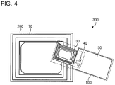
- Fig. 4 is a diagram illustrating a schematic configuration of a contactless power transmission system according to Embodiment 1.
- a contactless power transmission system 300 includes a power reception device 100 and a power transmission device 200 that transmits power to the power reception device 100.
- the power transmission device 200 includes a power transmission coil 70 that transmits power with magnetic resonance.
- the power transmission coil 70 is a flat coil in which a substrate wiring pattern such as copper foil is spirally formed. It should be noted that the power transmission coil 70 is not limited to the wiring pattern, and may be formed by spirally winding an arbitrary conductive wire. Also, the power transmission coil 70 may be formed by stacking a plurality of layers.
- Fig. 4 illustrates the case where the size of the power transmission coil 70 is greater than that of the power reception coil 30, the embodiment is not limited to this case, and the size of the power transmission coil 70 may be nearly equal to that of the power reception coil 30. Furthermore, the power reception coil 30 and the power transmission coil 70 may be circular or elliptical.
- the power reception coil 30 of the power reception device 100 When located within the range of a magnetic field produced by the power transmission coil 70, the power reception coil 30 of the power reception device 100 receives power through magnetic resonance. Power transmission using magnetic resonance will be described in detail with reference to Figs. 5 and 6 .
- Fig. 5 is a diagram illustrating configurations of the power transmission device and the power reception device according to Embodiment 1.
- Fig. 6 is a specific circuit diagram of the configuration as illustrated in Fig. 5 .
- the power reception device 100 and the power transmission device 200 are included in a magnetic resonance type of contactless power transmission system 300 that performs power transmission using resonance characteristics. That is, the power transmission device 200 is provided as a resonance type power transmission device that transmits power to the power reception device 100 through magnetic resonance.
- the power reception device 100 is provided as a resonance type power reception device that receives power from the power transmission device 200 through magnetic resonance. It should be noted that power transmission using magnetic resonance is also referred to as resonance coupling type power transmission.
- the power transmission device 200 includes a power transmission circuit 60 that forms an inverter circuit that supplies power to the power transmission coil 70.
- the power transmission circuit 60 includes a resonance type power supply 601 and a matching circuit 602.
- the resonance type power supply 601 controls supply of power to the power transmission coil 70, and converts input DC power or AC power into alternating current of a predetermined frequency and outputs the alternating current.
- the resonance type power supply 601 is a resonant switching power supply circuit that includes a semiconductor switching element S1.
- the resonance type power supply 601 has an output impedance Zo, a resonance frequency fo, and a resonance characteristic value Qo.
- the resonance frequency fo of the resonance type power supply 601 is set to a frequency in the MHz band.
- the resonance frequency fo is, for example, 6.78MHz. It should be noted that the resonance frequency fo is not limited to this, and may be a frequency that is an integral multiple of 6.78MHz in the MHz band.
- the matching circuit 602 performs impedance matching between an output impedance Zo of the resonance type power supply 601 and a pass characteristic impedance Zt of the power transmission coil 70.
- the matching circuit 602 includes a ⁇ or L filter including an inductor L and a capacitor C, and has a pass characteristic impedance Zp.
- the power transmission coil 70 When AC power is input from the resonance type power supply 601 to the power transmission coil 70 via the matching circuit 602, the power transmission coil 70 performs a resonance operation, and produces a non-radiation electromagnetic field in the vicinity of the power transmission coil 70, thereby transmitting power to the power reception coil 30 of the power reception device 100.
- the power transmission coil 70 forms along with a capacitor C5 form a resonance circuit.
- the power transmission coil 70 serves as a resonant antenna.
- the power transmission coil 70 has the pass characteristic impedance Zt, a resonance frequency ft, and a resonance characteristic value Qt.
- the resonance frequency fo and the resonance characteristic value Qo of the resonance type power supply 601 depend on the output impedance Zo of the resonance type power supply 601 and the pass characteristic impedance Zp of the matching circuit 602.
- a resonance frequency ft and the resonance characteristic value Qt of the power transmission coil 70 depend on the pass characteristic impedance Zt of the power transmission coil 70 and the pass characteristic impedance Zp of the matching circuit 602.
- the power reception circuit 40 of the power reception device 100 includes a rectifier circuit 401 and a conversion circuit 402.
- the power reception coil 30 receives power by performing a resonance coupling operation with a non-radiation electromagnetic field from the power transmission coil 70, and outputs AC power.
- the power reception coil 30 forms along with a capacitor C11 form a resonance circuit.
- the power reception coil 30 serves as a resonant antenna.
- the power reception coil 30 has a pass characteristic impedance Zr.
- the rectifier circuit 401 is a matching type rectifier circuit that has a rectifying function to convert AC power from the power reception coil 30 into DC power, and a matching function to perform impedance matching between the pass characteristic impedance Zr of the power reception coil 30 and the input impedance ZRL of the conversion circuit 402.
- the matching function is fulfilled by a ⁇ or L filter that includes an inductor L and a capacitor C.
- the rectifier circuit 401 has a pass characteristic impedance Zs. Although it is described above that the rectifier circuit 401 has the rectifier function and the matching function, it is not limitative.
- the rectifier circuit 401 may be configured to have the rectifying function only, though such a configuration causes a rectification efficiency to be reduced.
- the conversion circuit 402 receives DC power from the rectifier circuit 401, converts the DC power into a predetermined voltage, and applies the voltage to the load circuit 50.
- the conversion circuit 402 includes an LC filter, a DC/DC converter, etc., and has an input impedance ZRL.
- the LC filter smooths a high-frequency voltage ripple, and the DC/DC converter performs conversion to obtain a predetermined voltage. It should be noted that the conversion circuit 402 may be formed to include the LC filter only, which is a smoothing filter, without including the DC/DC converter.
- a resonance characteristic value Qr and a resonance frequency fr of the power reception device 100 depend on the pass characteristic impedance Zr of the power reception coil 30, the pass characteristic impedance Zs of the rectifier circuit 401, and the input impedance ZRL of the conversion circuit 402.
- the three resonance characteristic values that are the resonance characteristic value Qo of the resonance type power supply 601, the resonance characteristic value Qt of the power transmission coil 70, and the resonance characteristic value Qr of the power reception device 100 are correlated with each other as indicated above, whereby a decrease in power transmission efficiency can be reduced. Therefore, in the power transmission by the magnetic resonance method, the distance between the power transmission coil 70 and the power reception coil 30 can be increased as compared with the power transmission by the electromagnetic induction method. It should be noted that the power transmission by the electromagnetic induction method is also referred to as electromagnetic induction coupling type power transmission.
- the semiconductor switching element S1 is formed of, for example, a wide-bandgap semiconductor.
- a wide-bandgap semiconductor is a general term for semiconductor elements having a larger bandgap than that of silicon.
- the wide-bandgap semiconductor is silicon carbide, a gallium-nitride-based material, diamond, or gallium nitride.
- the semiconductor switching element S1 is formed of a wide-bandgap semiconductor, the conduction loss of the semiconductor switching element S1 can be reduced. In addition, even when the switching frequency at which the semiconductor switching element S1 is driven is set to a high frequency, heat dissipation at the resonance type power supply 601 is satisfactory. Therefore, a radiating fin provided in the resonance type power supply 601 can be made smaller, and the resonance type power supply 601 can be made smaller and manufactured at a lower cost.
- a user places the power reception device 100 on the power transmission device 200.
- the power reception device 100 is placed such that the power reception coil 30 of the power reception device 100 faces the power transmission coil 70 of the power transmission device 200.
- the distance within which the power transmission can be achieved is long.
- the position of the power reception coil 30 is not limited to a position at which the power reception coil 30 faces the power transmission coil 70, and it suffices that the power reception coil 30 is located within a range in which the power reception coil 30 can receive power from the power transmission coil 70 using magnetic resonance.
- the power transmission circuit 60 of the power transmission device 200 When the power transmission circuit 60 of the power transmission device 200 operates, a high-frequency current is supplied from the power transmission circuit 60 to the power transmission coil 70, and a magnetic field is thus produced from the power transmission coil 70. As a result, power is supplied from the power transmission coil 70 to the power reception coil 30 of the power reception device 100 using magnetic resonance. The power received by the power reception coil 30 is converted into direct current by the power reception circuit 40, and the direct current is supplied to the load circuit 50.
- Fig. 7 is a diagram for explaining the positions of the load circuit and a magnetic field that acts on the power reception of the power reception coil of the contactless power transmission system according to Embodiment 1.
- a magnetic field produced in the axial direction of the power transmission coil 70 passes through the power reception coil 30, which is provided opposite to the power transmission coil 70.
- the magnetic field B1 passes through the power reception coil 30, a high-frequency induced voltage is produced in the power reception coil 30.
- the load circuit 50 is mounted on the second substrate 20.
- the second substrate 20 is located outside the power reception coil 30 as viewed in the direction along the axis AX of the power reception coil 30. That is, the magnetic field B1 that acts on the power reception of the power reception coil 30 does not pass through the load circuit 50.
- the power reception coil 30 is not magnetically affected by the load circuit 50, and a flux linkage of the power reception coil 30 is not reduced. It is therefore possible to improve a contactless power feeding efficiency. This is because even if the distance between the power transmission device 200 and the power reception device 100 is great, it is possible to produce an induced voltage in the power reception coil 30 and also to operate the load circuit 50, thereby improving the usability of the contactless power transmission system 300.
- Fig. 8 is a diagram for explaining the positions of the load circuit and a magnetic field that acts on the power reception of the power reception coil of the contactless power transmission system according to Embodiment 1.
- a magnetic field B3 is produced from the load circuit 50.
- an electrical current-loop path that is, an electrically closed circuit
- electrical components such as an LED or a microcomputer that form the load circuit 50 and a wiring pattern such as copper foil that electrically connects the electronic component.
- the load circuit 50 is mounted on the second substrate 20.
- the second substrate 20 is located outside the power reception coil 30 as viewed in the direction along the axis AX of the power reception coil 30.
- the magnetic field B3 produced from the load circuit 50 does not pass through the power reception coil 30, and the magnetic field B1 that acts on the power reception of the power reception coil 30 is not canceled by the magnetic field B3 that acts in the opposite direction to the direction where the magnetic field B1 acts.
- the power reception coil 30 is not magnetically affected by the load circuit 50, and the flux linkage of the power reception coil 30 is not reduced. It is therefore possible to improve a contactless power feeding efficiency. This is because even if the distance between the power transmission device 200 and the power reception device 100 is great, it is possible to produce an induced voltage in the power reception coil 30 and also to operate the load circuit 50, thereby improving the usability of the contactless power transmission system 300.
- the power reception device 100 includes the first substrate 10 on which the power reception coil 30 and the power reception circuit 40 are mounted, and the second substrate 20 which is provided outside the power reception coil 30 as viewed in the direction along the axis AX of the power reception coil 30 and on which the load circuit 50 is mounted.
- the inductance of a connection path between the power reception coil 30 and the power reception circuit 40 can be reduced to a small value, as compared with the case where the power reception circuit 40 is mounted on the second substrate 20 which is provided separate from the first substrate 10. It is therefore possible to reduce a power loss and a high-frequency noise between the power reception coil 30 that receives power using magnetic resonance and the power reception circuit 40.
- the magnetic field B3 produced from the load circuit 50 does not cancel the magnetic field B1 acting on the power reception of the power reception coil 30.
- the distance between the power reception coil 30 and the load circuit 50 does not need to be set great. Also, since it is not necessary to provide, for example, a magnetic sheet between the power reception coil 30 and the load circuit 50, it is possible to improve the contactless power feeding efficiency and to make the power reception device 100 smaller. In addition, since it is not necessary to provide a shield plate or a magnetic sheet, the manufacturing cost of the power reception device can be reduced.
- an electrically closed circuit can be provided in the load circuit 50, it is possible to improve the flexibility in designing the wiring pattern on the second substrate 20 on which the load circuit 50 is mounted. Therefore, the number of components provided on the load circuit 50 mounted on the second substrate 20 can be increased, and the performance of the power reception device 100 can be made higher.
- the first region 12 in which the power reception coil 30 is located is adjacent to the second region 13 in which the power reception circuit 40 is located, as viewed in the direction along the axis AX of the power reception coil 30. That is, the power reception coil 30 and the power reception circuit 40 are provided on the first substrate 10 such that the wiring pattern connecting the power reception coil 30 and the power reception circuit 40 is set to have the shortest possible length.
- the inductance of the connection path between the power reception coil 30 and the power reception circuit 40 can be reduced. It is therefore possible to reduce a power loss and a high-frequency noise between the power reception coil 30 and the power reception circuit 40 which receive power by magnetic resonance.
- the power reception circuit 40 on the first substrate 10 is covered by at least part of the second substrate 20 as viewed in the direction along the axis AX of the power reception coil 30.
- the length of the wire 21 connecting the power reception circuit 40 and the load circuit 50 can be shortened.
- the power reception device 100 can be made small, as compared with the case where the first substrate 10 and the second substrate 20 are provided such that they do not overlap with each other.
- the restriction on the position of the power reception device 100 to which power is transmitted from the power transmission device 200 can be reduced, as compared with the power transmission is performed by the electromagnetic induction coupling.
- the power transmission coil 70 and the power reception coil 30 are not provided to face each other, power transmission can be achieved. Therefore, it is possible to improve the flexibility in setting the position of the power reception device 100 and to improve the usability.
- Embodiment 2 a configuration in which the power reception device 100 is applied to a remote controller will be described.
- Embodiment 1 components that are the same as those in Embodiment 1 will be denoted by the same reference numerals, and Embodiment 2 will be described by referring mainly to the differences between Embodiments 1 and 2.
- Fig. 9 is a plan view illustrating an external appearance of the power reception device according to Embodiment 2.
- Fig. 10 is a plan view schematically illustrating an internal configuration of the power reception device according to Embodiment 2.
- Fig. 11 is a diagram schematically illustrating a cross section taken along line A-A in Fig. 10 .
- the power reception device 100 also functions as a remote controller.
- the power reception device 100 includes a load circuit 50 and a second load circuit 51 that are supplied with power from the power reception circuit 40.
- the load circuit 50 includes electronic component such a microcomputer and an operation switch that performs an operation related to an operation input to the remote controller. Furthermore, the load circuit 50 includes electronic component that form a transmission unit and a reception unit. The transmission unit transmits operation information to an external device, and the reception unit acquires information from the external device.
- the second load circuit 51 is provided in such a manner to overlap with the power reception coil 30 as viewed in the direction along the axis AX of the power reception coil 30.
- the second load circuit 51 is provided in the housing 1 of the power reception device 100 in such a manner as to face the power reception coil 30 and adjacent to the second substrate 20.
- the second load circuit 51 displays information on an operation input by the load circuit 50 or information acquired from an external device.
- the second load circuit 51 includes, for example, a display component such as a liquid crystal display (LCD) or a light emitting diode (LED).
- the second load circuit 51 includes a component that does not form an electrically closed circuit. It should be noted that “does not form an electrically closed circuit” means that there is no passage through which current flows in a loop manner.
- the second load circuit 51 includes an electronic component which does not form an electrically closed circuit, and is provided in such a manner as to overlap with the power reception coil 30 as viewed in the direction along the axis AX of the power reception coil 30.
- the volume of the housing 1 of the power reception device 100 can be effectively used. Furthermore, the second load circuit 51 does not form an electrically closed circuit. Thus, even when a magnetic field from the power transmission coil 70 passes through the second load circuit 51, current does not flow in a loop manner, a magnetic field that cancels the flux linkage of the power reception coil 30 is not produced from the second load circuit 51, and there is no possibility that the contactless power feeding efficiency will be reduced.
- the volume of the power reception device 100 by providing in a region that faces the power reception coil 30, a component that is not affected by the supply of power to the power reception coil 30, and also possible to provide the power reception device 100 which is compact and easily usable.
- the second load circuit 51 includes a display component, it is not limitative. Any component or components can be used as the second load circuit 51 as long as the components have a configuration in which a current loop is not provided.
- the second load circuit 51 includes an LCD or an LED as the display component
- a microcomputer that controls the operation of the display component may be provided in the load circuit 50
- the display component may be provided in the second load circuit 51
- the display component may be electrically connected to the load circuit 50 of the second substrate 20.
- the second load circuit 51 is not limited to electronic components.
- the second load circuit 51 may include a light guide plate.
- the load circuit 50 mounted on the second substrate 20 includes, for example, an LED as the display component, and light from the LED is made incident on the light guide plate, which is provided on an upper surface of the power reception coil 30.
- a backlight of the display unit may be formed to include the light guide plate which is included in the second load circuit 51.
- Embodiment 3 a plurality of sets of power reception coils 30 and power reception circuits 40 are provided, and this will be described as follows.
- Embodiment 3 will be described by referring mainly to the differences between Embodiment 3 and Embodiments 1 and 2.
- Fig. 12 is a plan view schematically illustrating an internal configuration of a power reception device according to Embodiment 3.
- the power reception device 101 includes a first substrate 10a on which a power reception coil 30a and a power reception circuit 40b are mounted, and a first substrate 10b on which a power reception coil 30b and a power reception circuit 40b are mounted.
- the load circuit 50 mounted on the second substrate 20 is supplied with power from both the power reception circuit 40a and the power reception circuit 40b.
- the second substrate 20 is provided outside the power reception coil 30a as viewed in the direction along the axis AX of the power reception coil 30a. Also, the second substrate 20 is provided outside the power reception coil 30b as viewed in the direction along the axis AX of the power reception coil 30b.
- Fig. 13 is a diagram for explaining the positions of the load circuit and a magnetic field that acts on the power reception of the power reception coil of a contactless power transmission system according to Embodiment 3.
- a magnetic field produced in the axial direction of the power transmission coil 70 passes through the power reception coil 30a.
- a high-frequency induced voltage is produced in the power reception coil 30a.
- a magnetic field produced in the axial direction of the power transmission coil 70 passes through the power reception coil 30b.
- a high-frequency induced voltage is produced in the power reception coil 30b.
- a magnetic field B3 is produced from the load circuit 50. That is, when the magnetic field B2 passes through an electrically closed circuit provided in the load circuit 50, current flows through the electrically closed circuit of the load circuit 50, and the magnetic field B3 is produced in the opposite direction to the direction of the magnetic field B2.
- the load circuit 50 is mounted on the second substrate 20.
- the second substrate 20 is located outside the power reception coil 30a as viewed in the direction along the axis AX of the power reception coil 30a. Also, the second substrate 20 is located outside the power reception coil 30b as viewed in the direction along the axis AX of the power reception coil 30b.
- the magnetic field B3 produced from the load circuit 50 passes through neither the power reception coil 30a nor the power reception coil 30b.
- the power reception coils 30a and 30b are not magnetically affected by the load circuit 50, and the flux linkages of the power reception coils 30a and 30b are not reduced. Therefore, it is possible to improve the contactless power feeding efficiency.
- Embodiment 3 although the above description refers to the case where two sets of power reception coils 30 and power reception circuits 40 are provided, the embodiment is not limited to such a case, that is, an arbitrary number of sets of power reception coils and power reception circuits 40 may be provided.
- the first substrate 10 and the second substrate 20 are movable, and this configuration will be described as follows.
- Embodiment 4 will be described by referring mainly to the differences between Embodiment 4 and Embodiments 1 to 3.
- Figs. 14 and 15 are plan views schematically illustrating a configuration of a power reception device according to Embodiment 4.
- Fig. 14 is a diagram illustrating a state in which a first housing 1a and a second housing 1b, which will be described later, have been moved to a first position.
- Fig. 15 is a diagram illustrating a state in which the first housing 1a and the second housing 1b have been moved to a second position.
- Fig. 14, (a), and Fig. 15, (a) are plan views schematically illustrating an internal configuration of the power reception device 102
- Fig. 14, (b), and Fig. 15, (b) are schematic diagrams illustrating a side surface of the power reception device 102.
- the power reception device 102 includes a first housing 1a that houses the first substrate 10 and a second housing 1b that houses the second substrate 20.
- the first housing 1a and the second housing 1b are connected to each other such that the first and second housings 1a and 1b can be moved to a first position where the load circuit 50 is located outside the power reception coil 30 and a second position where the load circuit 50 overlaps with the power reception coil 30, as viewed from the direction of the axis AX of the power reception coil 30.
- movable slide mechanisms are attached to the first housing 1a and the second housing 1b, and the first housing 1a is configured to slide relative to the second housing 1b.
- the user moves the first housing 1a to the first position. In the case where the power reception device 102 does not receive power from the power transmission device 200, the user moves the first housing 1a to the second position.
- the power reception device 102 can obtain the same advantages as in Embodiments 1 to 3.
- the power reception device 102 can be made smaller, and the usability of the power reception device 102 is improved.
- first housing 1a is configured to slide relative to the second housing 1b
- first housing 1a and the second housing 1b may be rotatably connected each other.
- end portions of the first housing 1a and the second housing 1b may be connected to each other by a hinge mechanism such that that the first and second housings 1a and 1b are rotatable. That is, any configuration can be applied as long as the first housing 1a and the second housing 1b can be moved to the first position where the load circuit 50 is located outside the power reception coil 30 and the second position where the load circuit 50 overlaps with the power reception coil 30.
- Fig. 16 is a side view schematically illustrating a modification of the configuration of the power reception device according to Embodiment 4.
- the second load circuit 51 that does not form an electrically closed circuit may be provided on the first housing 1a.
- the second load circuit 51 is provided in such a manner as to overlap with the power reception coil 30 as viewed in the direction along the axis AX of the power reception coil 30.
Landscapes
- Engineering & Computer Science (AREA)
- Computer Networks & Wireless Communication (AREA)
- Power Engineering (AREA)
- Physics & Mathematics (AREA)
- Electromagnetism (AREA)
- Signal Processing (AREA)
- Charge And Discharge Circuits For Batteries Or The Like (AREA)
- Near-Field Transmission Systems (AREA)
Abstract
Description
- The present disclosure relates to a power reception device that receives power in a contactless manner and according to a magnetic resonance method, and a contactless power transmission system including the power reception device.
- In the related art, a cellular phone including the following power reception coil and circuit board is provided. The power reception coil receives power transferred from a power transmission coil using electromagnetic induction, and on the circuit board, a conversion circuit is mounted to convert alternating current induced in the power reception coil into direct current and output the direct current (see, for example, Patent Literature 1). This cellular phone includes a movable case that houses the power reception coil and a main-body case that houses the circuit board, and the movable case and the main-body case are provided as separate cases. The movable case is coupled to the main-body case such that the power reception coil can be separated from the circuit board.
- Furthermore, in the related art, a wireless power transmission system is provided which transmits power using magnetic field resonance between a power transmission coil and a power reception coil (see, for example, Patent Literature 2). In a magnetic field resonance method, a power transmission device and a power reception device are provided with respective resonance circuits each employing a coil and a capacitor, and the resonance frequencies of these resonance circuits are made to coincide with each other, whereby power is transmitted from the power transmission device to the power reception device. In wireless power transmission by the magnetic field resonance method, it is possible to transmit power with a high efficiency even if the power transmission device and the power reception device are separated from each other to a certain extent. It should be noted that the magnetic field resonance is also referred to as magnetic resonance.
-
- Patent Literature 1: Japanese Unexamined Patent Application Publication No.
2013-78243 - Patent Literature 2: Japanese Patent No.
5838562 - In the technique described in
Patent Literature 1, the movable case that houses the power reception coil is provided apart from the circuit board, thereby preventing the circuit board from malfunctioning because of electromagnetic wave noise of the power transmission coil. However, in the technique ofPatent Literature 1, since power is transmitted by an electromagnetic induction method, the distance between the power transmission coil and the power reception coil needs to be short, as compared with the power transmission by the magnetic resonance method, and the position of the power reception device is restricted. - On the other hand, in the power transmission of the magnetic resonance method, for example, in that of the wireless transmission system described in Patent Literature 2, the distance between the power transmission coil and the power reception coil can be set great, as compared with the power transmission by the electromagnetic induction method, and the restriction on the position of the power reception device can be reduced.
- However, if the power transmission by the magnetic resonance method is applied to the technique described in
Patent Literature 1, such a combination gives rise to the following problems. - The frequency of power transmitted by magnetic resonance is higher than that of power transmitted by electromagnetic induction. For example, the frequency of power transmitted by electromagnetic induction is in the kHz band, whereas the resonance frequency of magnetic resonance is in the MHz band.
- Thus, a loss caused by an inductance of a wire such as a lead connecting a power reception coil housed in a movable case and a circuit board (power reception circuit) housed in a main-body case is increased. Furthermore, a high-frequency noise is made in the wire such as the lead connecting the power reception coil and the circuit board, and causes the circuit board to malfunction.
- The present disclosure is applied to solve the above problems, and relates to a power reception device and a contactless power transmission system that can reduce a power loss and a high-frequency noise between a power reception coil that receives power through magnetic resonance and a power reception circuit.
- A power reception device according to an embodiment of the present disclosure includes: a power reception coil that receives power by magnetic resonance; a power reception circuit that converts power received by the power reception coil into direct current; a load circuit that operates by the directed current into which the power is converted by the power reception circuit; a first substrate on which the power reception coil and the power reception circuit are mounted; and a second substrate on which the load circuit is mounted, the second substrate being located outside the power reception coil as viewed in an axial direction of the power reception coil.
- In the power reception device according to the embodiment of the present disclosure, the power reception coil and the power reception circuit are mounted on the first substrate. Therefore, the inductance of a connection path between the power reception coil and the power reception circuit can be reduced to a small value, and a power loss and a high-frequency noise can be reduced, as compared with the case where the power reception circuit is mounted on the second substrate, which is provided separate from the first substrate.
-
- [
Fig. 1] Fig. 1 is a plan view schematically illustrating an internal configuration of a power reception device according to a first embodiment. - [
Fig. 2] Fig. 2 is a diagram schematically illustrating a cross section taken along line A-A inFig. 1 . - [Fi. 3]
Fig. 3 is a plan view for explaining the positions of a power reception coil and a power reception circuit of the power reception device according toEmbodiment 1. - [
Fig. 4] Fig. 4 is a diagram schematically illustrating a schematic configuration of a contactless power transmission system according toEmbodiment 1. - [
Fig. 5] Fig. 5 is a diagram illustrating a configuration of a power transmission device and the power reception device according toEmbodiment 1. - [
Fig. 6] Fig. 6 is a specific circuit diagram of the configuration as illustrated inFig. 5 . - [
Fig. 7] Fig. 7 is a diagram illustrating the positions of a load circuit and a magnetic field that acts on the power reception coil of the contactless power transmission system according toEmbodiment 1. - [
Fig. 8] Fig. 8 is a diagram for explaining the positions of the load circuit and the magnetic field that acts on the power reception coil of the contactless power transmission system according toEmbodiment 1. - [
Fig. 9] Fig. 9 is a plan view illustrating an external appearance of a power reception device according to Embodiment 2. - [
Fig. 10] Fig. 10 is a plan view schematically illustrating an internal configuration of the power reception device according to Embodiment 2. - [
Fig. 11] Fig. 11 is a diagram schematically illustrating a cross section taken along line A-A inFig. 10 . - [
Fig. 12] Fig. 12 is a plan view schematically illustrating an internal configuration of a power reception device according to Embodiment 3. - [
Fig. 13] Fig. 13 is a diagram for explaining the positions of a lord circuit and a magnetic field that acts on a power reception coil of a contactless power transmission system according to Embodiment 3. - [
Fig. 14] Fig. 14 is a plan view schematically illustrating a configuration of a power reception device according to Embodiment 4. - [
Fig. 15] Fig. 15 is another plan view schematically illustrating the configuration of the power reception device according to Embodiment 4. - [
Fig. 16] Fig. 16 is a side view illustrating a modification of the configuration of the power reception device according to Embodiment 4. -
Fig. 1 is a plan view schematically illustrating an internal configuration of a power reception device according toEmbodiment 1. -
Fig. 2 is a diagram schematically illustrating a cross section taken along line A-A inFig. 1 . - As illustrated in
Figs. 1 and 2 , apower reception device 100 includes afirst substrate 10 and asecond substrate 20 both housed in ahousing 1. - On the
first substrate 10, apower reception coil 30 and apower reception circuit 40 are mounted. - The
power reception coil 30 receives power through magnetic resonance. Thepower reception coil 30 is a flat coil in which a wiring pattern such as copper foil is spirally formed. It should be noted that thepower reception coil 30 is not limited to the wiring pattern, and may be formed by spirally winding an arbitrary conductive line and may be mounted on thefirst substrate 10. Furthermore, thepower reception coil 30 may be formed to have a plurality of layers stacked. - It should be noted that at an inner peripheral portion of the
power reception coil 30 on thefirst substrate 10, acutout portion 11, which is a through hole extending through thefirst substrate 10, is formed. It should be noted that it is not indispensable that thecutout portion 11 is formed; that is, nocutout portion 11 may be provided. - The
power reception circuit 40 converts power received by thepower reception coil 30 into direct current. A detailed configuration of the circuit configuration will be described later. - The
power reception coil 30 and thepower reception circuit 40 are connected by a wiring pattern formed on thefirst substrate 10. The positions of thepower reception coil 30 and thepower reception circuit 40 on thefirst substrate 10 will be described with reference toFig. 3 . -
Fig. 3 is a plan view for explaining the positions of the power reception coil and the power reception circuit of the power reception device according toEmbodiment 1. - As illustrated in
Fig. 3 , at thefirst substrate 10, afirst region 12 and asecond region 13 are adjacent to each other as viewed in a direction along an axis AX of thepower reception coil 30; and in thefirst region 12, thepower reception coil 30 is provided, and in thesecond region 13, thepower reception circuit 40 is provided. That is, thepower reception coil 30 and thepower reception circuit 40 are provided on thefirst substrate 10 such that the wiring pattern connecting thepower reception coil 30 and thepower reception circuit 40 is set to have the shortest possible length. - The following description is made with reference to
Figs. 1 and 2 . - On the
second substrate 20, aload circuit 50 is mounted. Theload circuit 50 is operated by the direct current obtained by conversion performed by thepower reception circuit 40. Theload circuit 50 and thepower reception circuit 40 are connected by awire 21. Thewire 21 is, for example, a conductive line that is made of an arbitrary metal coated with an insulating film. - The
second substrate 20 is provided outside thepower reception coil 30 as viewed in the direction along the axis AX of thepower reception coil 30. For example, as illustrated inFig. 2 , thesecond substrate 20 is provided such that an end of thesecond substrate 20 that is closer to thepower reception coil 30 is separated from an outer peripheral end of thepower reception coil 30 by a distance G. - The
power reception circuit 40 on thefirst substrate 10 overlaps with at least part of thesecond substrate 20 as viewed in the direction along the axis AX of thepower reception coil 30. -
Fig. 4 is a diagram illustrating a schematic configuration of a contactless power transmission system according toEmbodiment 1. - As illustrated in
Fig. 4 ,a contactlesspower transmission system 300 includes apower reception device 100 and apower transmission device 200 that transmits power to thepower reception device 100. - The
power transmission device 200 includes apower transmission coil 70 that transmits power with magnetic resonance. - The
power transmission coil 70 is a flat coil in which a substrate wiring pattern such as copper foil is spirally formed. It should be noted that thepower transmission coil 70 is not limited to the wiring pattern, and may be formed by spirally winding an arbitrary conductive wire. Also, thepower transmission coil 70 may be formed by stacking a plurality of layers. - It should be noted that although
Fig. 4 illustrates the case where the size of thepower transmission coil 70 is greater than that of thepower reception coil 30, the embodiment is not limited to this case, and the size of thepower transmission coil 70 may be nearly equal to that of thepower reception coil 30. Furthermore, thepower reception coil 30 and thepower transmission coil 70 may be circular or elliptical. - When located within the range of a magnetic field produced by the
power transmission coil 70, thepower reception coil 30 of thepower reception device 100 receives power through magnetic resonance. Power transmission using magnetic resonance will be described in detail with reference toFigs. 5 and6 . -
Fig. 5 is a diagram illustrating configurations of the power transmission device and the power reception device according toEmbodiment 1. -
Fig. 6 is a specific circuit diagram of the configuration as illustrated inFig. 5 . - The
power reception device 100 and thepower transmission device 200 are included in a magnetic resonance type of contactlesspower transmission system 300 that performs power transmission using resonance characteristics. That is, thepower transmission device 200 is provided as a resonance type power transmission device that transmits power to thepower reception device 100 through magnetic resonance. Thepower reception device 100 is provided as a resonance type power reception device that receives power from thepower transmission device 200 through magnetic resonance. It should be noted that power transmission using magnetic resonance is also referred to as resonance coupling type power transmission. - As illustrated in
Figs. 5 and6 , thepower transmission device 200 includes apower transmission circuit 60 that forms an inverter circuit that supplies power to thepower transmission coil 70. - The
power transmission circuit 60 includes a resonancetype power supply 601 and amatching circuit 602. - The resonance
type power supply 601 controls supply of power to thepower transmission coil 70, and converts input DC power or AC power into alternating current of a predetermined frequency and outputs the alternating current. The resonancetype power supply 601 is a resonant switching power supply circuit that includes a semiconductor switching element S1. The resonancetype power supply 601 has an output impedance Zo, a resonance frequency fo, and a resonance characteristic value Qo. The resonance frequency fo of the resonancetype power supply 601 is set to a frequency in the MHz band. The resonance frequency fo is, for example, 6.78MHz. It should be noted that the resonance frequency fo is not limited to this, and may be a frequency that is an integral multiple of 6.78MHz in the MHz band. - The
matching circuit 602 performs impedance matching between an output impedance Zo of the resonancetype power supply 601 and a pass characteristic impedance Zt of thepower transmission coil 70. Thematching circuit 602 includes a π or L filter including an inductor L and a capacitor C, and has a pass characteristic impedance Zp. - When AC power is input from the resonance
type power supply 601 to thepower transmission coil 70 via thematching circuit 602, thepower transmission coil 70 performs a resonance operation, and produces a non-radiation electromagnetic field in the vicinity of thepower transmission coil 70, thereby transmitting power to thepower reception coil 30 of thepower reception device 100. Thepower transmission coil 70 forms along with a capacitor C5 form a resonance circuit. Thepower transmission coil 70 serves as a resonant antenna. Thepower transmission coil 70 has the pass characteristic impedance Zt, a resonance frequency ft, and a resonance characteristic value Qt. - The resonance frequency fo and the resonance characteristic value Qo of the resonance
type power supply 601 depend on the output impedance Zo of the resonancetype power supply 601 and the pass characteristic impedance Zp of thematching circuit 602. A resonance frequency ft and the resonance characteristic value Qt of thepower transmission coil 70 depend on the pass characteristic impedance Zt of thepower transmission coil 70 and the pass characteristic impedance Zp of thematching circuit 602. - From the two resonance characteristic values Qo and Qt, the
power transmission device 200 has a resonance characteristic value Qtx as indicated by the following equation (1).
[Math. 1]
- The
power reception circuit 40 of thepower reception device 100 includes arectifier circuit 401 and aconversion circuit 402. - The
power reception coil 30 receives power by performing a resonance coupling operation with a non-radiation electromagnetic field from thepower transmission coil 70, and outputs AC power. Thepower reception coil 30 forms along with a capacitor C11 form a resonance circuit. Thepower reception coil 30 serves as a resonant antenna. Thepower reception coil 30 has a pass characteristic impedance Zr. - The
rectifier circuit 401 is a matching type rectifier circuit that has a rectifying function to convert AC power from thepower reception coil 30 into DC power, and a matching function to perform impedance matching between the pass characteristic impedance Zr of thepower reception coil 30 and the input impedance ZRL of theconversion circuit 402. The matching function is fulfilled by a π or L filter that includes an inductor L and a capacitor C. Therectifier circuit 401 has a pass characteristic impedance Zs. Although it is described above that therectifier circuit 401 has the rectifier function and the matching function, it is not limitative. Therectifier circuit 401 may be configured to have the rectifying function only, though such a configuration causes a rectification efficiency to be reduced. - The
conversion circuit 402 receives DC power from therectifier circuit 401, converts the DC power into a predetermined voltage, and applies the voltage to theload circuit 50. Theconversion circuit 402 includes an LC filter, a DC/DC converter, etc., and has an input impedance ZRL. The LC filter smooths a high-frequency voltage ripple, and the DC/DC converter performs conversion to obtain a predetermined voltage. It should be noted that theconversion circuit 402 may be formed to include the LC filter only, which is a smoothing filter, without including the DC/DC converter. - A resonance characteristic value Qr and a resonance frequency fr of the
power reception device 100 depend on the pass characteristic impedance Zr of thepower reception coil 30, the pass characteristic impedance Zs of therectifier circuit 401, and the input impedance ZRL of theconversion circuit 402. - The characteristic impedances of functional units are set such that the resonance characteristic value Qo of the resonance
type power supply 601, the resonance characteristic value Qt of thepower transmission coil 70, and the resonance characteristic value Qr of thepower reception device 100 have a correlation. That is, the resonance characteristic value Qtx (=√(Qo·Qt)) of thepower transmission device 200 and the resonance characteristic value Qr of thepower reception device 100 are approximated to each other (formula (2) below). - Specifically, the range indicated by the following formula (3) is desirable.
[Math. 2]

- As described above, the three resonance characteristic values that are the resonance characteristic value Qo of the resonance
type power supply 601, the resonance characteristic value Qt of thepower transmission coil 70, and the resonance characteristic value Qr of thepower reception device 100 are correlated with each other as indicated above, whereby a decrease in power transmission efficiency can be reduced. Therefore, in the power transmission by the magnetic resonance method, the distance between thepower transmission coil 70 and thepower reception coil 30 can be increased as compared with the power transmission by the electromagnetic induction method. It should be noted that the power transmission by the electromagnetic induction method is also referred to as electromagnetic induction coupling type power transmission. - The semiconductor switching element S1 is formed of, for example, a wide-bandgap semiconductor. A wide-bandgap semiconductor is a general term for semiconductor elements having a larger bandgap than that of silicon. The wide-bandgap semiconductor is silicon carbide, a gallium-nitride-based material, diamond, or gallium nitride.
- Since the semiconductor switching element S1 is formed of a wide-bandgap semiconductor, the conduction loss of the semiconductor switching element S1 can be reduced. In addition, even when the switching frequency at which the semiconductor switching element S1 is driven is set to a high frequency, heat dissipation at the resonance
type power supply 601 is satisfactory. Therefore, a radiating fin provided in the resonancetype power supply 601 can be made smaller, and the resonancetype power supply 601 can be made smaller and manufactured at a lower cost. - Next, the operation of the contactless
power transmission system 300 according toEmbodiment 1 will be described. - A user places the
power reception device 100 on thepower transmission device 200. For example, thepower reception device 100 is placed such that thepower reception coil 30 of thepower reception device 100 faces thepower transmission coil 70 of thepower transmission device 200. It should be noted that as described above, in the power transmission by the magnetic resonance method, the distance within which the power transmission can be achieved is long. Thus, the position of thepower reception coil 30 is not limited to a position at which thepower reception coil 30 faces thepower transmission coil 70, and it suffices that thepower reception coil 30 is located within a range in which thepower reception coil 30 can receive power from thepower transmission coil 70 using magnetic resonance. - When the
power transmission circuit 60 of thepower transmission device 200 operates, a high-frequency current is supplied from thepower transmission circuit 60 to thepower transmission coil 70, and a magnetic field is thus produced from thepower transmission coil 70. As a result, power is supplied from thepower transmission coil 70 to thepower reception coil 30 of thepower reception device 100 using magnetic resonance. The power received by thepower reception coil 30 is converted into direct current by thepower reception circuit 40, and the direct current is supplied to theload circuit 50. - It will be described how a magnetic field that acts on power reception of the
power reception coil 30 affects theload circuit 50. -
Fig. 7 is a diagram for explaining the positions of the load circuit and a magnetic field that acts on the power reception of the power reception coil of the contactless power transmission system according toEmbodiment 1. - As illustrated in
Fig. 7 , a magnetic field produced in the axial direction of thepower transmission coil 70 passes through thepower reception coil 30, which is provided opposite to thepower transmission coil 70. When the magnetic field B1 passes through thepower reception coil 30, a high-frequency induced voltage is produced in thepower reception coil 30. - As illustrated in
Figs. 1 and 2 , theload circuit 50 is mounted on thesecond substrate 20. Thesecond substrate 20 is located outside thepower reception coil 30 as viewed in the direction along the axis AX of thepower reception coil 30. That is, the magnetic field B1 that acts on the power reception of thepower reception coil 30 does not pass through theload circuit 50. - Thus, the
power reception coil 30 is not magnetically affected by theload circuit 50, and a flux linkage of thepower reception coil 30 is not reduced. It is therefore possible to improve a contactless power feeding efficiency. This is because even if the distance between thepower transmission device 200 and thepower reception device 100 is great, it is possible to produce an induced voltage in thepower reception coil 30 and also to operate theload circuit 50, thereby improving the usability of the contactlesspower transmission system 300. -
Fig. 8 is a diagram for explaining the positions of the load circuit and a magnetic field that acts on the power reception of the power reception coil of the contactless power transmission system according toEmbodiment 1. - As illustrated in
Fig. 8 , when the magnetic field B2 from thepower transmission coil 70 passes through theload circuit 50, a magnetic field B3 is produced from theload circuit 50. To be more specific, at theload circuit 50, an electrical current-loop path, that is, an electrically closed circuit, is provided by electrical components such as an LED or a microcomputer that form theload circuit 50 and a wiring pattern such as copper foil that electrically connects the electronic component. When the magnetic field B2 passes through the electrically closed circuit provided at theload circuit 50, a high-frequency induced voltage is produced. Then, current flows through the electrically closed circuit of theload circuit 50, thereby producing a magnetic field B3 that acts in the opposite direction to a direction where the magnetic field B2 acts. - As illustrated in
Figs. 1 and 2 , theload circuit 50 is mounted on thesecond substrate 20. Thesecond substrate 20 is located outside thepower reception coil 30 as viewed in the direction along the axis AX of thepower reception coil 30. - That is, the magnetic field B3 produced from the
load circuit 50 does not pass through thepower reception coil 30, and the magnetic field B1 that acts on the power reception of thepower reception coil 30 is not canceled by the magnetic field B3 that acts in the opposite direction to the direction where the magnetic field B1 acts. - Thus, the
power reception coil 30 is not magnetically affected by theload circuit 50, and the flux linkage of thepower reception coil 30 is not reduced. It is therefore possible to improve a contactless power feeding efficiency. This is because even if the distance between thepower transmission device 200 and thepower reception device 100 is great, it is possible to produce an induced voltage in thepower reception coil 30 and also to operate theload circuit 50, thereby improving the usability of the contactlesspower transmission system 300. - As described above, in
Embodiment 1, thepower reception device 100 includes thefirst substrate 10 on which thepower reception coil 30 and thepower reception circuit 40 are mounted, and thesecond substrate 20 which is provided outside thepower reception coil 30 as viewed in the direction along the axis AX of thepower reception coil 30 and on which theload circuit 50 is mounted. - Therefore, the inductance of a connection path between the
power reception coil 30 and thepower reception circuit 40 can be reduced to a small value, as compared with the case where thepower reception circuit 40 is mounted on thesecond substrate 20 which is provided separate from thefirst substrate 10. It is therefore possible to reduce a power loss and a high-frequency noise between thepower reception coil 30 that receives power using magnetic resonance and thepower reception circuit 40. - Furthermore, since a wire such as a lead that connects the
power reception coil 30 and thepower reception circuit 40 is unnecessary, it is possible to reduce the frequency of occurrence of high-frequency noise and also that of occurrence of malfunction of theload circuit 50. - Furthermore, even if an electrically closed circuit is provided in the
load circuit 50, the magnetic field B3 produced from theload circuit 50 does not cancel the magnetic field B1 acting on the power reception of thepower reception coil 30. - Therefore, the distance between the
power reception coil 30 and theload circuit 50 does not need to be set great. Also, since it is not necessary to provide, for example, a magnetic sheet between thepower reception coil 30 and theload circuit 50, it is possible to improve the contactless power feeding efficiency and to make thepower reception device 100 smaller. In addition, since it is not necessary to provide a shield plate or a magnetic sheet, the manufacturing cost of the power reception device can be reduced. - Furthermore, since an electrically closed circuit can be provided in the
load circuit 50, it is possible to improve the flexibility in designing the wiring pattern on thesecond substrate 20 on which theload circuit 50 is mounted. Therefore, the number of components provided on theload circuit 50 mounted on thesecond substrate 20 can be increased, and the performance of thepower reception device 100 can be made higher. - In
Embodiment 1, in thefirst substrate 10, thefirst region 12 in which thepower reception coil 30 is located is adjacent to thesecond region 13 in which thepower reception circuit 40 is located, as viewed in the direction along the axis AX of thepower reception coil 30. That is, thepower reception coil 30 and thepower reception circuit 40 are provided on thefirst substrate 10 such that the wiring pattern connecting thepower reception coil 30 and thepower reception circuit 40 is set to have the shortest possible length. - Thus, the inductance of the connection path between the
power reception coil 30 and thepower reception circuit 40 can be reduced. It is therefore possible to reduce a power loss and a high-frequency noise between thepower reception coil 30 and thepower reception circuit 40 which receive power by magnetic resonance. - Moreover, in
Embodiment 1, thepower reception circuit 40 on thefirst substrate 10 is covered by at least part of thesecond substrate 20 as viewed in the direction along the axis AX of thepower reception coil 30. - Therefore, the length of the
wire 21 connecting thepower reception circuit 40 and theload circuit 50 can be shortened. In addition, thepower reception device 100 can be made small, as compared with the case where thefirst substrate 10 and thesecond substrate 20 are provided such that they do not overlap with each other. - In the contactless
power transmission system 300 according toEmbodiment 1, power is transmitted from thepower transmission device 200 to thepower reception device 100 using magnetic resonance. - Therefore, the restriction on the position of the
power reception device 100 to which power is transmitted from thepower transmission device 200 can be reduced, as compared with the power transmission is performed by the electromagnetic induction coupling. In addition, even in the case where thepower transmission coil 70 and thepower reception coil 30 are not provided to face each other, power transmission can be achieved. Therefore, it is possible to improve the flexibility in setting the position of thepower reception device 100 and to improve the usability. - In Embodiment 2, a configuration in which the
power reception device 100 is applied to a remote controller will be described. - It should be noted that components that are the same as those in
Embodiment 1 will be denoted by the same reference numerals, and Embodiment 2 will be described by referring mainly to the differences betweenEmbodiments 1 and 2. -
Fig. 9 is a plan view illustrating an external appearance of the power reception device according to Embodiment 2. -
Fig. 10 is a plan view schematically illustrating an internal configuration of the power reception device according to Embodiment 2. -
Fig. 11 is a diagram schematically illustrating a cross section taken along line A-A inFig. 10 . - As illustrated in
Figs. 9 to 11 , thepower reception device 100 according to Embodiment 2 also functions as a remote controller. Thepower reception device 100 includes aload circuit 50 and asecond load circuit 51 that are supplied with power from thepower reception circuit 40. - The
load circuit 50 includes electronic component such a microcomputer and an operation switch that performs an operation related to an operation input to the remote controller. Furthermore, theload circuit 50 includes electronic component that form a transmission unit and a reception unit. The transmission unit transmits operation information to an external device, and the reception unit acquires information from the external device. - The
second load circuit 51 is provided in such a manner to overlap with thepower reception coil 30 as viewed in the direction along the axis AX of thepower reception coil 30. For example, thesecond load circuit 51 is provided in thehousing 1 of thepower reception device 100 in such a manner as to face thepower reception coil 30 and adjacent to thesecond substrate 20. - The
second load circuit 51 displays information on an operation input by theload circuit 50 or information acquired from an external device. Thesecond load circuit 51 includes, for example, a display component such as a liquid crystal display (LCD) or a light emitting diode (LED). Thesecond load circuit 51 includes a component that does not form an electrically closed circuit. It should be noted that "does not form an electrically closed circuit" means that there is no passage through which current flows in a loop manner. - As described above, in Embodiment 2, the
second load circuit 51 includes an electronic component which does not form an electrically closed circuit, and is provided in such a manner as to overlap with thepower reception coil 30 as viewed in the direction along the axis AX of thepower reception coil 30. - Therefore, the volume of the
housing 1 of thepower reception device 100 can be effectively used. Furthermore, thesecond load circuit 51 does not form an electrically closed circuit. Thus, even when a magnetic field from thepower transmission coil 70 passes through thesecond load circuit 51, current does not flow in a loop manner, a magnetic field that cancels the flux linkage of thepower reception coil 30 is not produced from thesecond load circuit 51, and there is no possibility that the contactless power feeding efficiency will be reduced. - Therefore, it is possible to effectively use the volume of the
power reception device 100 by providing in a region that faces thepower reception coil 30, a component that is not affected by the supply of power to thepower reception coil 30, and also possible to provide thepower reception device 100 which is compact and easily usable. - Although it is described above by way of example that the
second load circuit 51 includes a display component, it is not limitative. Any component or components can be used as thesecond load circuit 51 as long as the components have a configuration in which a current loop is not provided. - In the case where the
second load circuit 51 includes an LCD or an LED as the display component, for example, a microcomputer that controls the operation of the display component may be provided in theload circuit 50, the display component may be provided in thesecond load circuit 51, and the display component may be electrically connected to theload circuit 50 of thesecond substrate 20. - The
second load circuit 51 is not limited to electronic components. For example, thesecond load circuit 51 may include a light guide plate. To be more specific, in this case, theload circuit 50 mounted on thesecond substrate 20 includes, for example, an LED as the display component, and light from the LED is made incident on the light guide plate, which is provided on an upper surface of thepower reception coil 30. In such a manner, a backlight of the display unit may be formed to include the light guide plate which is included in thesecond load circuit 51. - In Embodiment 3, a plurality of sets of power reception coils 30 and
power reception circuits 40 are provided, and this will be described as follows. - It should be noted that components that are the same as those in
Embodiments 1 and/or 2 will be denoted by the same reference numerals, and Embodiment 3 will be described by referring mainly to the differences between Embodiment 3 and Embodiments 1 and 2. -
Fig. 12 is a plan view schematically illustrating an internal configuration of a power reception device according to Embodiment 3. - As illustrated in
Fig. 12 , in Embodiment 3, thepower reception device 101 includes afirst substrate 10a on which apower reception coil 30a and apower reception circuit 40b are mounted, and afirst substrate 10b on which apower reception coil 30b and apower reception circuit 40b are mounted. Theload circuit 50 mounted on thesecond substrate 20 is supplied with power from both thepower reception circuit 40a and thepower reception circuit 40b. - The
second substrate 20 is provided outside thepower reception coil 30a as viewed in the direction along the axis AX of thepower reception coil 30a. Also, thesecond substrate 20 is provided outside thepower reception coil 30b as viewed in the direction along the axis AX of thepower reception coil 30b. -
Fig. 13 is a diagram for explaining the positions of the load circuit and a magnetic field that acts on the power reception of the power reception coil of a contactless power transmission system according to Embodiment 3. - As illustrated in
Fig. 13 , a magnetic field produced in the axial direction of thepower transmission coil 70 passes through thepower reception coil 30a. When the magnetic field B1a passes through thepower reception coil 30a, a high-frequency induced voltage is produced in thepower reception coil 30a. - Also, a magnetic field produced in the axial direction of the
power transmission coil 70 passes through thepower reception coil 30b. When the magnetic field B1b passes through thepower reception coil 30b, a high-frequency induced voltage is produced in thepower reception coil 30b. - Furthermore, when the magnetic field B2 from the
power transmission coil 70 passes through theload circuit 50, a magnetic field B3 is produced from theload circuit 50. That is, when the magnetic field B2 passes through an electrically closed circuit provided in theload circuit 50, current flows through the electrically closed circuit of theload circuit 50, and the magnetic field B3 is produced in the opposite direction to the direction of the magnetic field B2. - The
load circuit 50 is mounted on thesecond substrate 20. Thesecond substrate 20 is located outside thepower reception coil 30a as viewed in the direction along the axis AX of thepower reception coil 30a. Also, thesecond substrate 20 is located outside thepower reception coil 30b as viewed in the direction along the axis AX of thepower reception coil 30b. - That is, the magnetic field B3 produced from the
load circuit 50 passes through neither thepower reception coil 30a nor thepower reception coil 30b. Thus, the power reception coils 30a and 30b are not magnetically affected by theload circuit 50, and the flux linkages of the power reception coils 30a and 30b are not reduced. Therefore, it is possible to improve the contactless power feeding efficiency. - With respect to Embodiment 3, although the above description refers to the case where two sets of power reception coils 30 and
power reception circuits 40 are provided, the embodiment is not limited to such a case, that is, an arbitrary number of sets of power reception coils andpower reception circuits 40 may be provided. - As described above, since a plurality of sets of power reception coils 30 and
power reception circuits 40 are provided in thepower reception device 100, it is possible to enlarge the space in thepower reception device 100 where the power reception coils 30 are provided, and also to enlarge the range in which power can be transmitted by thepower reception device 100. Therefore, the usability can be further improved. - In Embodiment 4, the
first substrate 10 and thesecond substrate 20 are movable, and this configuration will be described as follows. - It should be noted that components that are the same as those of any of
Embodiments 1 to 3 will be denoted by the same reference signs, and Embodiment 4 will be described by referring mainly to the differences between Embodiment 4 andEmbodiments 1 to 3. -
Figs. 14 and15 are plan views schematically illustrating a configuration of a power reception device according to Embodiment 4.Fig. 14 is a diagram illustrating a state in which afirst housing 1a and asecond housing 1b, which will be described later, have been moved to a first position.Fig. 15 is a diagram illustrating a state in which thefirst housing 1a and thesecond housing 1b have been moved to a second position. It should be noted thatFig. 14, (a), and Fig. 15, (a) , are plan views schematically illustrating an internal configuration of thepower reception device 102, andFig. 14, (b), and Fig. 15, (b) , are schematic diagrams illustrating a side surface of thepower reception device 102. - As illustrated in
Figs. 14 and15 , in Embodiment 4, thepower reception device 102 includes afirst housing 1a that houses thefirst substrate 10 and asecond housing 1b that houses thesecond substrate 20. - In the
power reception device 102, as viewed from the direction of the axis AX of thepower reception coil 30, thefirst housing 1a and thesecond housing 1b are connected to each other such that the first andsecond housings load circuit 50 is located outside thepower reception coil 30 and a second position where theload circuit 50 overlaps with thepower reception coil 30, as viewed from the direction of the axis AX of thepower reception coil 30. - For example, as illustrated in
Figs. 14 and15 , movable slide mechanisms are attached to thefirst housing 1a and thesecond housing 1b, and thefirst housing 1a is configured to slide relative to thesecond housing 1b. - Because of the above configuration, in the case where the
power reception device 102 receives power from thepower transmission device 200, the user moves thefirst housing 1a to the first position. In the case where thepower reception device 102 does not receive power from thepower transmission device 200, the user moves thefirst housing 1a to the second position. - Thus, when the
first housing 1a is located at the first position, thepower reception device 102 can obtain the same advantages as inEmbodiments 1 to 3. - Furthermore, in the case where the
first housing 1a is located at the second position, thepower reception device 102 can be made smaller, and the usability of thepower reception device 102 is improved. - Although the above description refers to the case where the
first housing 1a is configured to slide relative to thesecond housing 1b, it is not restrictive. For example, thefirst housing 1a and thesecond housing 1b may be rotatably connected each other. In addition, end portions of thefirst housing 1a and thesecond housing 1b may be connected to each other by a hinge mechanism such that that the first andsecond housings first housing 1a and thesecond housing 1b can be moved to the first position where theload circuit 50 is located outside thepower reception coil 30 and the second position where theload circuit 50 overlaps with thepower reception coil 30. -
Fig. 16 is a side view schematically illustrating a modification of the configuration of the power reception device according to Embodiment 4. As illustrated inFig. 16 , thesecond load circuit 51 that does not form an electrically closed circuit may be provided on thefirst housing 1a. As in Embodiment 2, thesecond load circuit 51 is provided in such a manner as to overlap with thepower reception coil 30 as viewed in the direction along the axis AX of thepower reception coil 30. - Also, in such a configuration, it is possible to effectively use the volume in the
power reception device 102, and provide thepower reception device 102 which is compact and easily usable. - 1 housing, 1a first housing, 1b second housing, 10 first substrate, 10a first substrate, 10b first substrate, 11 cutout portion, 12 first region, 13 second region, 20 second substrate, 21 wire, 30 power reception coil, 30a power reception coil, 30b power reception coil, 40 power reception circuit, 40a power reception circuit, 40b power reception circuit, 50 load circuit, 51 second load circuit, 60 power transmission circuit, 65 power transmission coil, 70 power transmission coil, 80 power reception coil, 100 power reception device, 101 power reception device, 102 power reception device, 200 power transmission device, 300 contactless power transmission system, 401 rectifier circuit, 402 conversion circuit, 601 resonance type power supply, 602 matching circuit
Claims (11)
- A power reception device comprising:a power reception coil configured to receive power through magnetic resonance;a power reception circuit configured to convert power received by the power reception coil into direct current;a load circuit configured to operate by the direct current obtained by conversion performed by the power reception circuit;a first substrate on which the power reception coil and the power reception circuit are mounted; anda second substrate on which the load circuit is mounted, the second substrate being located outside the power reception coil as viewed in an axial direction of the power reception coil.
- The power reception device of claim 1, wherein the first substrate includes a first region in which the power reception coil is provided and a second region in which the power reception circuit is provided, and the first region and the second region are adjacent to each other as viewed in the axial direction of the power reception coil.
- The power reception device of claim 1 or 2, wherein the power reception circuit mounted on the first substrate overlaps with at least part of the second substrate as viewed in the axial direction of the power reception coil.
- The power reception device of any one of claims 1 to 3, further comprising a second load circuit configured to operate by the direct current obtained by the conversion performed by the power reception circuit,
wherein the second load circuit is located to overlap with the power reception coil as viewed in the axial direction of the power reception coil, and includes a component which does not form an electrically closed circuit. - The power reception device of any one of claims 1 to 4, comprising a plurality of sets of the power reception coils and the power reception circuits,
wherein the load circuit is configured to receive power from the plurality of sets of the power reception coils and the power reception circuits. - The power reception device of any one of claims 1 to 5, further comprising:a first housing that houses the first substrate; anda second housing that houses the second substrate,wherein the first housing and the second housing are connected to each other such that the first housing and the second housing are movable to a first position where the load circuit is located outside the power reception coil and a second position where the load circuit overlaps with the power reception coil, as viewed in the axial direction of the power reception coil.
- The power reception device of any one of claims 1 to 6, wherein a resonance frequency of the magnetic resonance is in a MHz band.
- The power reception device of claim 7, wherein the resonance frequency of the magnetic resonance is 6.78 MHz or an integral multiple of 6.78 MHz.
- A contactless power transmission system comprising:a power transmission device including a power transmission coil and an inverter circuit, the power transmission coil being configured to transmit power through magnetic resonance, the inverter circuit configured to supply power to the power transmission coil; andthe power reception device of any one of claims 1 to 8.
- The contactless power transmission system of claim 9, wherein the inverter circuit includes a semiconductor switching element, and the semiconductor switching element is formed of a wide-bandgap semiconductor.
- The contactless power transmission system of claim 10, wherein the wide-bandgap semiconductor is silicon carbide, a gallium-nitride-based material, diamond, or gallium nitride.
Applications Claiming Priority (1)
| Application Number | Priority Date | Filing Date | Title |
|---|---|---|---|
| PCT/JP2017/039096 WO2019087237A1 (en) | 2017-10-30 | 2017-10-30 | Power reception device and non-contact power transmission system |
Publications (3)
| Publication Number | Publication Date |
|---|---|
| EP3706286A1 true EP3706286A1 (en) | 2020-09-09 |
| EP3706286A4 EP3706286A4 (en) | 2020-09-09 |
| EP3706286B1 EP3706286B1 (en) | 2023-09-20 |
Family
ID=66332977
Family Applications (1)
| Application Number | Title | Priority Date | Filing Date |
|---|---|---|---|
| EP17930775.6A Active EP3706286B1 (en) | 2017-10-30 | 2017-10-30 | Power reception device and non-contact power transmission system |
Country Status (5)
| Country | Link |
|---|---|
| US (1) | US11101697B2 (en) |
| EP (1) | EP3706286B1 (en) |
| JP (1) | JP6873263B2 (en) |
| CN (1) | CN111247711B (en) |
| WO (1) | WO2019087237A1 (en) |
Families Citing this family (1)
| Publication number | Priority date | Publication date | Assignee | Title |
|---|---|---|---|---|
| JP7488466B2 (en) * | 2020-09-07 | 2024-05-22 | タイガー魔法瓶株式会社 | Electric rice cooker |
Family Cites Families (25)
| Publication number | Priority date | Publication date | Assignee | Title |
|---|---|---|---|---|
| JPS5838562B2 (en) | 1977-09-06 | 1983-08-24 | 積水樹脂株式会社 | Assembly road construction method and construction measurement equipment |
| JPH1198706A (en) * | 1997-09-18 | 1999-04-09 | Tokin Corp | Non-contact charger |
| JP2006314181A (en) * | 2005-05-09 | 2006-11-16 | Sony Corp | Non-contact charger, non-contact charging system, and non-contact charging method |
| KR101372963B1 (en) * | 2006-01-31 | 2014-03-11 | 히타치 긴조쿠 가부시키가이샤 | Laminated component and module using same |
| US7994889B2 (en) * | 2006-06-01 | 2011-08-09 | Taiyo Yuden Co., Ltd. | Multilayer inductor |
| JP5362568B2 (en) * | 2006-09-18 | 2013-12-11 | コーニンクレッカ フィリップス エヌ ヴェ | Apparatus, system and method for electromagnetic energy transfer |
| US20110050164A1 (en) * | 2008-05-07 | 2011-03-03 | Afshin Partovi | System and methods for inductive charging, and improvements and uses thereof |
| US8810194B2 (en) * | 2008-11-20 | 2014-08-19 | Qualcomm Incorporated | Retrofitting wireless power and near-field communication in electronic devices |
| CN102782937B (en) * | 2010-03-03 | 2016-02-17 | 株式会社村田制作所 | Wireless communication devices and wireless communication terminal |
| JP2011210937A (en) * | 2010-03-30 | 2011-10-20 | Murata Mfg Co Ltd | Coil module and electronic device having the same |
| JP2012075283A (en) * | 2010-09-29 | 2012-04-12 | Murata Mfg Co Ltd | Power transmission system and power transmission device |
| KR101414779B1 (en) * | 2010-10-20 | 2014-07-03 | 한국전자통신연구원 | Wireless power transfer device |
| JP2012130139A (en) * | 2010-12-14 | 2012-07-05 | Tanashin Denki Co | Magnetic induction coil moving type contactless charger |
| JP5838562B2 (en) | 2011-02-17 | 2016-01-06 | 富士通株式会社 | Wireless power transmission device and wireless power transmission system |
| US8970069B2 (en) * | 2011-03-28 | 2015-03-03 | Tdk Corporation | Wireless power receiver and wireless power transmission system |
| JP2014116988A (en) * | 2011-03-30 | 2014-06-26 | Sanyo Electric Co Ltd | Battery charging cradle |
| JP2012223027A (en) * | 2011-04-12 | 2012-11-12 | Sanyo Electric Co Ltd | Non-contact type charging adaptor |
| JP5790200B2 (en) | 2011-06-27 | 2015-10-07 | ソニー株式会社 | Communication apparatus and communication system |
| JP2013013204A (en) | 2011-06-28 | 2013-01-17 | Toshiba Corp | Wireless power transmission system, power transmission device and power reception device |
| JP2013078243A (en) | 2011-09-30 | 2013-04-25 | Sanyo Electric Co Ltd | Portable device incorporating power reception coil |
| JP5809943B2 (en) * | 2011-11-25 | 2015-11-11 | 東芝機械株式会社 | Linear motor |
| CN104969442B (en) * | 2013-02-15 | 2017-09-05 | 株式会社村田制作所 | Wireless power supply |
| JP2016220268A (en) * | 2015-05-14 | 2016-12-22 | 竹内工業株式會社 | Non-contact power supply device |
| JP6541425B2 (en) * | 2015-05-18 | 2019-07-10 | 株式会社テクノバ | Wireless power supply system |
| JP2016129482A (en) * | 2016-02-29 | 2016-07-14 | 中国電力株式会社 | Non-contact power supply system, power transmission device, and power reception device |
-
2017
- 2017-10-30 US US16/756,339 patent/US11101697B2/en active Active
- 2017-10-30 EP EP17930775.6A patent/EP3706286B1/en active Active
- 2017-10-30 JP JP2019549992A patent/JP6873263B2/en active Active
- 2017-10-30 WO PCT/JP2017/039096 patent/WO2019087237A1/en unknown
- 2017-10-30 CN CN201780096118.0A patent/CN111247711B/en active Active
Also Published As
| Publication number | Publication date |
|---|---|
| WO2019087237A1 (en) | 2019-05-09 |
| US11101697B2 (en) | 2021-08-24 |
| JP6873263B2 (en) | 2021-05-19 |
| EP3706286A4 (en) | 2020-09-09 |
| CN111247711B (en) | 2024-02-13 |
| US20200244107A1 (en) | 2020-07-30 |
| JPWO2019087237A1 (en) | 2020-10-22 |
| CN111247711A (en) | 2020-06-05 |
| EP3706286B1 (en) | 2023-09-20 |
Similar Documents
| Publication | Publication Date | Title |
|---|---|---|
| US10367267B2 (en) | Flexible printed circuit board for dual mode antennas, dual mode antenna and user device | |
| US10033089B2 (en) | Antenna device and electronic apparatus including antenna device | |
| US10158256B2 (en) | Contactless connector system tolerant of position displacement between transmitter coil and receiver coil and having high transmission efficiency | |
| US9805861B2 (en) | Communication terminal including close-proximity communication coil, power transmission coil, and metal plate | |
| EP2733787B1 (en) | Antenna device and communication terminal device | |
| JP6269902B2 (en) | ANTENNA DEVICE AND ELECTRONIC DEVICE | |
| EP2264831A1 (en) | Radio ic device, electronic device, and method for adjusting resonance frequency of radio ic device | |
| JP6696573B2 (en) | Wireless module, RFID system and wireless power supply device | |
| CN110620408A (en) | Wireless charger with electromagnetic shielding function | |
| US10263467B2 (en) | Antenna for wireless power, and dual mode antenna comprising same | |
| US8228252B2 (en) | Data coupler | |
| JP6583599B1 (en) | ANTENNA DEVICE, COMMUNICATION SYSTEM, AND ELECTRONIC DEVICE | |
| WO2019220818A1 (en) | Antenna device and electronic apparatus | |
| KR20140076993A (en) | Wireless power device | |
| EP3706286B1 (en) | Power reception device and non-contact power transmission system | |
| KR20140013015A (en) | Transmission coil for wireless power transmission | |
| KR101856564B1 (en) | Combo antenna module and mobile electronic device having the same | |
| JP6444510B2 (en) | Wireless power transmission apparatus and receiving apparatus | |
| CN210182579U (en) | Antenna device, non-contact transmission device, and non-contact transmission system | |
| JP2019201520A (en) | Electronic apparatus | |
| US11637460B2 (en) | Wireless power transfer system having an electric field shield member | |
| US20230124799A1 (en) | Wireless power transfer system | |
| KOUCHI et al. | The Wireless Feeding Flexible Printed Circuit Which is Available for the Curved Surface Mount |
Legal Events
| Date | Code | Title | Description |
|---|---|---|---|
| STAA | Information on the status of an ep patent application or granted ep patent |
Free format text: STATUS: THE INTERNATIONAL PUBLICATION HAS BEEN MADE |
|
| PUAI | Public reference made under article 153(3) epc to a published international application that has entered the european phase |
Free format text: ORIGINAL CODE: 0009012 |
|
| STAA | Information on the status of an ep patent application or granted ep patent |
Free format text: STATUS: REQUEST FOR EXAMINATION WAS MADE |
|
| 17P | Request for examination filed |
Effective date: 20200423 |
|
| A4 | Supplementary search report drawn up and despatched |
Effective date: 20200805 |
|
| AK | Designated contracting states |
Kind code of ref document: A1 Designated state(s): AL AT BE BG CH CY CZ DE DK EE ES FI FR GB GR HR HU IE IS IT LI LT LU LV MC MK MT NL NO PL PT RO RS SE SI SK SM TR |
|
| AX | Request for extension of the european patent |
Extension state: BA ME |
|
| DAV | Request for validation of the european patent (deleted) | ||
| DAX | Request for extension of the european patent (deleted) | ||
| STAA | Information on the status of an ep patent application or granted ep patent |
Free format text: STATUS: EXAMINATION IS IN PROGRESS |
|
| 17Q | First examination report despatched |
Effective date: 20210811 |
|
| STAA | Information on the status of an ep patent application or granted ep patent |
Free format text: STATUS: EXAMINATION IS IN PROGRESS |
|
| GRAP | Despatch of communication of intention to grant a patent |
Free format text: ORIGINAL CODE: EPIDOSNIGR1 |
|
| STAA | Information on the status of an ep patent application or granted ep patent |
Free format text: STATUS: GRANT OF PATENT IS INTENDED |
|
| INTG | Intention to grant announced |
Effective date: 20230405 |
|
| P01 | Opt-out of the competence of the unified patent court (upc) registered |
Effective date: 20230512 |
|
| GRAS | Grant fee paid |
Free format text: ORIGINAL CODE: EPIDOSNIGR3 |
|
| GRAA | (expected) grant |
Free format text: ORIGINAL CODE: 0009210 |
|
| STAA | Information on the status of an ep patent application or granted ep patent |
Free format text: STATUS: THE PATENT HAS BEEN GRANTED |
|
| AK | Designated contracting states |
Kind code of ref document: B1 Designated state(s): AL AT BE BG CH CY CZ DE DK EE ES FI FR GB GR HR HU IE IS IT LI LT LU LV MC MK MT NL NO PL PT RO RS SE SI SK SM TR |
|
| REG | Reference to a national code |
Ref country code: GB Ref legal event code: FG4D |
|
| REG | Reference to a national code |
Ref country code: CH Ref legal event code: EP |
|
| REG | Reference to a national code |
Ref country code: IE Ref legal event code: FG4D |
|
| REG | Reference to a national code |
Ref country code: DE Ref legal event code: R096 Ref document number: 602017074555 Country of ref document: DE |
|
| REG | Reference to a national code |
Ref country code: LT Ref legal event code: MG9D |
|
| PG25 | Lapsed in a contracting state [announced via postgrant information from national office to epo] |
Ref country code: GR Free format text: LAPSE BECAUSE OF FAILURE TO SUBMIT A TRANSLATION OF THE DESCRIPTION OR TO PAY THE FEE WITHIN THE PRESCRIBED TIME-LIMIT Effective date: 20231221 |
|
| REG | Reference to a national code |
Ref country code: NL Ref legal event code: MP Effective date: 20230920 |
|
| PG25 | Lapsed in a contracting state [announced via postgrant information from national office to epo] |
Ref country code: SE Free format text: LAPSE BECAUSE OF FAILURE TO SUBMIT A TRANSLATION OF THE DESCRIPTION OR TO PAY THE FEE WITHIN THE PRESCRIBED TIME-LIMIT Effective date: 20230920 Ref country code: RS Free format text: LAPSE BECAUSE OF FAILURE TO SUBMIT A TRANSLATION OF THE DESCRIPTION OR TO PAY THE FEE WITHIN THE PRESCRIBED TIME-LIMIT Effective date: 20230920 Ref country code: NO Free format text: LAPSE BECAUSE OF FAILURE TO SUBMIT A TRANSLATION OF THE DESCRIPTION OR TO PAY THE FEE WITHIN THE PRESCRIBED TIME-LIMIT Effective date: 20231220 Ref country code: LV Free format text: LAPSE BECAUSE OF FAILURE TO SUBMIT A TRANSLATION OF THE DESCRIPTION OR TO PAY THE FEE WITHIN THE PRESCRIBED TIME-LIMIT Effective date: 20230920 Ref country code: LT Free format text: LAPSE BECAUSE OF FAILURE TO SUBMIT A TRANSLATION OF THE DESCRIPTION OR TO PAY THE FEE WITHIN THE PRESCRIBED TIME-LIMIT Effective date: 20230920 Ref country code: HR Free format text: LAPSE BECAUSE OF FAILURE TO SUBMIT A TRANSLATION OF THE DESCRIPTION OR TO PAY THE FEE WITHIN THE PRESCRIBED TIME-LIMIT Effective date: 20230920 Ref country code: GR Free format text: LAPSE BECAUSE OF FAILURE TO SUBMIT A TRANSLATION OF THE DESCRIPTION OR TO PAY THE FEE WITHIN THE PRESCRIBED TIME-LIMIT Effective date: 20231221 Ref country code: FI Free format text: LAPSE BECAUSE OF FAILURE TO SUBMIT A TRANSLATION OF THE DESCRIPTION OR TO PAY THE FEE WITHIN THE PRESCRIBED TIME-LIMIT Effective date: 20230920 |
|
| PGFP | Annual fee paid to national office [announced via postgrant information from national office to epo] |
Ref country code: DE Payment date: 20231024 Year of fee payment: 7 |
|
| REG | Reference to a national code |
Ref country code: AT Ref legal event code: MK05 Ref document number: 1614171 Country of ref document: AT Kind code of ref document: T Effective date: 20230920 |
|
| PG25 | Lapsed in a contracting state [announced via postgrant information from national office to epo] |
Ref country code: NL Free format text: LAPSE BECAUSE OF FAILURE TO SUBMIT A TRANSLATION OF THE DESCRIPTION OR TO PAY THE FEE WITHIN THE PRESCRIBED TIME-LIMIT Effective date: 20230920 |
|
| PG25 | Lapsed in a contracting state [announced via postgrant information from national office to epo] |
Ref country code: IS Free format text: LAPSE BECAUSE OF FAILURE TO SUBMIT A TRANSLATION OF THE DESCRIPTION OR TO PAY THE FEE WITHIN THE PRESCRIBED TIME-LIMIT Effective date: 20240120 |
|
| PG25 | Lapsed in a contracting state [announced via postgrant information from national office to epo] |
Ref country code: AT Free format text: LAPSE BECAUSE OF FAILURE TO SUBMIT A TRANSLATION OF THE DESCRIPTION OR TO PAY THE FEE WITHIN THE PRESCRIBED TIME-LIMIT Effective date: 20230920 |
|
| PG25 | Lapsed in a contracting state [announced via postgrant information from national office to epo] |
Ref country code: ES Free format text: LAPSE BECAUSE OF FAILURE TO SUBMIT A TRANSLATION OF THE DESCRIPTION OR TO PAY THE FEE WITHIN THE PRESCRIBED TIME-LIMIT Effective date: 20230920 |
|
| PG25 | Lapsed in a contracting state [announced via postgrant information from national office to epo] |
Ref country code: SM Free format text: LAPSE BECAUSE OF FAILURE TO SUBMIT A TRANSLATION OF THE DESCRIPTION OR TO PAY THE FEE WITHIN THE PRESCRIBED TIME-LIMIT Effective date: 20230920 Ref country code: RO Free format text: LAPSE BECAUSE OF FAILURE TO SUBMIT A TRANSLATION OF THE DESCRIPTION OR TO PAY THE FEE WITHIN THE PRESCRIBED TIME-LIMIT Effective date: 20230920 Ref country code: IS Free format text: LAPSE BECAUSE OF FAILURE TO SUBMIT A TRANSLATION OF THE DESCRIPTION OR TO PAY THE FEE WITHIN THE PRESCRIBED TIME-LIMIT Effective date: 20240120 Ref country code: ES Free format text: LAPSE BECAUSE OF FAILURE TO SUBMIT A TRANSLATION OF THE DESCRIPTION OR TO PAY THE FEE WITHIN THE PRESCRIBED TIME-LIMIT Effective date: 20230920 Ref country code: EE Free format text: LAPSE BECAUSE OF FAILURE TO SUBMIT A TRANSLATION OF THE DESCRIPTION OR TO PAY THE FEE WITHIN THE PRESCRIBED TIME-LIMIT Effective date: 20230920 Ref country code: CZ Free format text: LAPSE BECAUSE OF FAILURE TO SUBMIT A TRANSLATION OF THE DESCRIPTION OR TO PAY THE FEE WITHIN THE PRESCRIBED TIME-LIMIT Effective date: 20230920 Ref country code: AT Free format text: LAPSE BECAUSE OF FAILURE TO SUBMIT A TRANSLATION OF THE DESCRIPTION OR TO PAY THE FEE WITHIN THE PRESCRIBED TIME-LIMIT Effective date: 20230920 Ref country code: SK Free format text: LAPSE BECAUSE OF FAILURE TO SUBMIT A TRANSLATION OF THE DESCRIPTION OR TO PAY THE FEE WITHIN THE PRESCRIBED TIME-LIMIT Effective date: 20230920 Ref country code: PT Free format text: LAPSE BECAUSE OF FAILURE TO SUBMIT A TRANSLATION OF THE DESCRIPTION OR TO PAY THE FEE WITHIN THE PRESCRIBED TIME-LIMIT Effective date: 20240122 |
|
| PG25 | Lapsed in a contracting state [announced via postgrant information from national office to epo] |
Ref country code: PL Free format text: LAPSE BECAUSE OF FAILURE TO SUBMIT A TRANSLATION OF THE DESCRIPTION OR TO PAY THE FEE WITHIN THE PRESCRIBED TIME-LIMIT Effective date: 20230920 Ref country code: IT Free format text: LAPSE BECAUSE OF FAILURE TO SUBMIT A TRANSLATION OF THE DESCRIPTION OR TO PAY THE FEE WITHIN THE PRESCRIBED TIME-LIMIT Effective date: 20230920 |
|
| REG | Reference to a national code |
Ref country code: CH Ref legal event code: PL |
|
| REG | Reference to a national code |
Ref country code: BE Ref legal event code: MM Effective date: 20231031 |
|
| PG25 | Lapsed in a contracting state [announced via postgrant information from national office to epo] |
Ref country code: LU Free format text: LAPSE BECAUSE OF NON-PAYMENT OF DUE FEES Effective date: 20231030 |
|
| REG | Reference to a national code |
Ref country code: DE Ref legal event code: R097 Ref document number: 602017074555 Country of ref document: DE |
|
| PG25 | Lapsed in a contracting state [announced via postgrant information from national office to epo] |
Ref country code: LU Free format text: LAPSE BECAUSE OF NON-PAYMENT OF DUE FEES Effective date: 20231030 |
|
| PG25 | Lapsed in a contracting state [announced via postgrant information from national office to epo] |
Ref country code: MC Free format text: LAPSE BECAUSE OF FAILURE TO SUBMIT A TRANSLATION OF THE DESCRIPTION OR TO PAY THE FEE WITHIN THE PRESCRIBED TIME-LIMIT Effective date: 20230920 |
|
| PG25 | Lapsed in a contracting state [announced via postgrant information from national office to epo] |
Ref country code: DK Free format text: LAPSE BECAUSE OF FAILURE TO SUBMIT A TRANSLATION OF THE DESCRIPTION OR TO PAY THE FEE WITHIN THE PRESCRIBED TIME-LIMIT Effective date: 20230920 |
|
| PG25 | Lapsed in a contracting state [announced via postgrant information from national office to epo] |
Ref country code: CH Free format text: LAPSE BECAUSE OF NON-PAYMENT OF DUE FEES Effective date: 20231031 |
|
| PLBE | No opposition filed within time limit |
Free format text: ORIGINAL CODE: 0009261 |
|
| STAA | Information on the status of an ep patent application or granted ep patent |
Free format text: STATUS: NO OPPOSITION FILED WITHIN TIME LIMIT |
|
| PG25 | Lapsed in a contracting state [announced via postgrant information from national office to epo] |
Ref country code: MC Free format text: LAPSE BECAUSE OF FAILURE TO SUBMIT A TRANSLATION OF THE DESCRIPTION OR TO PAY THE FEE WITHIN THE PRESCRIBED TIME-LIMIT Effective date: 20230920 Ref country code: DK Free format text: LAPSE BECAUSE OF FAILURE TO SUBMIT A TRANSLATION OF THE DESCRIPTION OR TO PAY THE FEE WITHIN THE PRESCRIBED TIME-LIMIT Effective date: 20230920 Ref country code: CH Free format text: LAPSE BECAUSE OF NON-PAYMENT OF DUE FEES Effective date: 20231031 |
|
| 26N | No opposition filed |
Effective date: 20240621 |
|
| GBPC | Gb: european patent ceased through non-payment of renewal fee |
Effective date: 20231220 |
|
| PG25 | Lapsed in a contracting state [announced via postgrant information from national office to epo] |
Ref country code: BE Free format text: LAPSE BECAUSE OF NON-PAYMENT OF DUE FEES Effective date: 20231031 |