JP2019201520A - Electronic apparatus - Google Patents
Electronic apparatus Download PDFInfo
- Publication number
- JP2019201520A JP2019201520A JP2018096154A JP2018096154A JP2019201520A JP 2019201520 A JP2019201520 A JP 2019201520A JP 2018096154 A JP2018096154 A JP 2018096154A JP 2018096154 A JP2018096154 A JP 2018096154A JP 2019201520 A JP2019201520 A JP 2019201520A
- Authority
- JP
- Japan
- Prior art keywords
- resonator
- power
- antenna unit
- dielectric substrate
- antenna
- Prior art date
- Legal status (The legal status is an assumption and is not a legal conclusion. Google has not performed a legal analysis and makes no representation as to the accuracy of the status listed.)
- Granted
Links
Images


Classifications
-
- Y—GENERAL TAGGING OF NEW TECHNOLOGICAL DEVELOPMENTS; GENERAL TAGGING OF CROSS-SECTIONAL TECHNOLOGIES SPANNING OVER SEVERAL SECTIONS OF THE IPC; TECHNICAL SUBJECTS COVERED BY FORMER USPC CROSS-REFERENCE ART COLLECTIONS [XRACs] AND DIGESTS
- Y02—TECHNOLOGIES OR APPLICATIONS FOR MITIGATION OR ADAPTATION AGAINST CLIMATE CHANGE
- Y02E—REDUCTION OF GREENHOUSE GAS [GHG] EMISSIONS, RELATED TO ENERGY GENERATION, TRANSMISSION OR DISTRIBUTION
- Y02E60/00—Enabling technologies; Technologies with a potential or indirect contribution to GHG emissions mitigation
- Y02E60/10—Energy storage using batteries
Abstract
Description
本開示は、電子機器に関する。 The present disclosure relates to an electronic device.
従来、電源が出力する電力を非接触で電気負荷に伝送するワイヤレス給電が知られている。この種のワイヤレス給電技術は、特に、携帯電話又は家電製品等の電子機器へのバッテリ充電に応用されている。 Conventionally, wireless power feeding that transmits power output from a power source to an electric load in a contactless manner is known. This type of wireless power supply technology is particularly applied to battery charging of electronic devices such as mobile phones or home appliances.
ワイヤレス給電の手法としては、外部空間から照射される電磁波に対してアンテナを共振させることにより当該電磁波の電力を回収する方法(以下、「アンテナ受電方式」と称する)、及び、共振器間における電磁結合を利用して送電装置から電力を回収する方法(以下、「共振器受電方式」と称する)等が知られている(例えば、特許文献1を参照)。 As a method of wireless power feeding, a method of collecting the power of the electromagnetic wave by resonating the antenna with respect to the electromagnetic wave irradiated from the external space (hereinafter referred to as “antenna power receiving method”), and an electromagnetic wave between the resonators A method of recovering electric power from a power transmission device using coupling (hereinafter, referred to as “resonator power receiving method”) or the like is known (for example, see Patent Document 1).
ところで、アンテナ受電方式は、複数の電子機器と同時に一括で充電等を実行し得る点で有用であるが、一方で単位時間当たりに回収し得る電力が小さく、充電時間が長くなるという問題を有する。 By the way, the antenna power receiving method is useful in that charging can be performed simultaneously with a plurality of electronic devices, but on the other hand, there is a problem that the power that can be collected per unit time is small and the charging time is long. .
一方、共振器受電方式は、単位時間当たりに回収し得る電力が大きく、充電時間の短縮化を図れる点で有用であるが、送電装置側の共振器と隣接して配置しなければならないため、充電器(即ち、送電装置の共振器)の持ち運び等の手間や不自由さが発生する。 On the other hand, the resonator power receiving method is useful in that the power that can be recovered per unit time is large and the charging time can be shortened, but it must be arranged adjacent to the resonator on the power transmission device side, Troubles and inconveniences such as carrying around the charger (that is, the resonator of the power transmission device) occur.
このように、アンテナ受電方式と共振器受電方式とは、利用態様が異なるため、電子機器においては、いずれの方式も適用し得るように、アンテナと共振器の両方を搭載し、使い手の都合や又は状況等に応じて簡単に切り替えられるようにすることが望ましい。 Thus, since the antenna power reception method and the resonator power reception method are different in usage, in an electronic device, both the antenna and the resonator are mounted so that either method can be applied. Alternatively, it is desirable to be able to switch easily according to the situation or the like.
本開示は、上記の問題点に鑑みてなされたもので、バッテリの充電等の際に共振器受電方式とアンテナ受電方式のいずれにも適用可能な電子機器を提供することを目的とする。 The present disclosure has been made in view of the above-described problems, and an object thereof is to provide an electronic device that can be applied to both a resonator power reception method and an antenna power reception method when charging a battery.
前述した課題を解決する主たる本開示は、
誘電体基板と、
前記誘電体基板の第1の領域に配設され、自身と対向して送電装置の共振器が配された際に当該送電装置の共振器と電磁結合することにより、当該送電装置から第1の高周波電力を受電する共振器と、
前記誘電体基板の第2の領域に配設され、外部空間から照射される電磁波との共振により、当該電磁波から第2の高周波電力を受電するアンテナ部と、
入力段に前記共振器と前記アンテナ部とが並列に接続されるように、前記誘電体基板の第3の領域に配設され、前記第1及び第2の高周波電力を整流して後段の電気負荷に出力する整流回路部と、
を備える電子機器である。
The main present disclosure for solving the above-described problems is as follows.
A dielectric substrate;
When the resonator of the power transmission device is disposed in the first region of the dielectric substrate and is opposed to the dielectric substrate, it is electromagnetically coupled to the resonator of the power transmission device, thereby causing the first from the power transmission device to A resonator that receives high-frequency power;
An antenna unit disposed in the second region of the dielectric substrate and receiving a second high-frequency power from the electromagnetic wave by resonance with the electromagnetic wave irradiated from an external space;
The resonator and the antenna unit are connected in parallel to the input stage, and are arranged in a third region of the dielectric substrate to rectify the first and second high-frequency powers and A rectifier circuit that outputs to a load;
Is an electronic device.
本開示に係る電子機器によれば、バッテリの充電等の際に共振器受電方式とアンテナ受電方式のいずれにも適用することができる。 The electronic device according to the present disclosure can be applied to both the resonator power reception method and the antenna power reception method when charging the battery.
以下に添付図面を参照しながら、本開示の好適な実施形態について詳細に説明する。尚、本明細書及び図面において、実質的に同一の機能を有する構成要素については、同一の符号を付することにより重複説明を省略する。 Hereinafter, preferred embodiments of the present disclosure will be described in detail with reference to the appended drawings. In the present specification and drawings, components having substantially the same function are denoted by the same reference numerals, and redundant description is omitted.
[電子機器の全体構成]
以下では、一例として、本発明を携帯電話に適用した態様について説明する。
[Overall configuration of electronic equipment]
Below, the aspect which applied this invention to the mobile phone is demonstrated as an example.
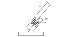
図1は、電子機器100の全体構成の一例を示す図である。図2は、電子機器100における共振器受電方式での受電態様の一例を示す図である。図3は、電子機器100におけるアンテナ受電方式での受電態様の一例を示す図である。
FIG. 1 is a diagram illustrating an example of the overall configuration of the
本実施形態に係る電子機器100は、共振器1、アンテナ部2、整流回路部3、誘電体基板4、及び、バッテリ5を備えている。
An
本実施形態に係る電子機器100は、バッテリ5の充電の際に、共振器1を用いた共振器受電方式、及び、アンテナ部2を用いたアンテナ受電方式のいずれにも適用することが可能な構成となっている。
The
電子機器100は、共振器受電方式で受電を実行する際には、図2に示すように、自身の共振器1が第1の送電装置200側の共振器201と対向するように、配置される。電子機器100は、この際には、共振器1と共振器201の間の電磁結合を利用して、第1の送電装置200から電力を回収する。これによって、大電力の受電が可能となり、バッテリ5への急速充電を実行することが可能となる。
The
第1の送電装置200は、例えば、商用電源(60Hz、100V)から高周波電力を生成する発振器(図示せず)、及び当該発振器からの高周波電力を取得する共振器201を含んで構成される。尚、第1の送電装置200の共振器201に送出される高周波電力の周波数は、典型的には、当該共振器201、及び、電子機器100の共振器1の共振周波数に対応する周波数(例えば、ミリ波帯域の特定の周波数)となるように設定される。
The first
一方、電子機器100は、アンテナ受電方式で受電を実行する際には、図3に示すように、第2の送電装置300によって送出された所定周波数の電磁波が伝搬される容器内に配置される。電子機器100は、この際には、アンテナ部2が当該電磁波と共振することにより、容器内に伝搬する電磁波の電力を回収する。これによって、電子機器100は、例えば、容器内に配置された他の電子機器(図3には、2つの電子機器100_1及び100_2を図示する)と共に、同時に、充電を実行することが可能である。
On the other hand, when the
第2の送電装置300は、例えば、容器内に、所定周波数の電磁波を放射するマグネトロン発振器、ガン発振器、又は半導体による発振器(例えば、インバータ)とアンプ等(図示せず)を含んで構成される。尚、第2の送電装置300から送出される高周波電力の周波数は、典型的には、電子機器100のアンテナ部2の共振周波数に対応する周波数(例えば、ミリ波帯域の特定の周波数)となるように設定される。
The second
次に、電子機器100の各部の構成について、詳述する。
Next, the configuration of each part of the
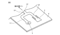
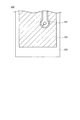
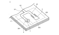
図4は、共振器1及びアンテナ部2の構成の一例を示す平面図である。図5は、共振器1及びアンテナ部2の構成の一例を示す斜視図である。図6は、共振器1及びアンテナ部2の構成の一例を示す側面断面図(図4のF−F’の位置における側面断面図)である。図7は、共振器1の構成の一例を示す拡大図である。
FIG. 4 is a plan view showing an example of the configuration of the
誘電体基板4は、共振器1、アンテナ部2、及び、整流回路部3等が配設される基板である。誘電体基板4内には、これらの各部品(共振器1、アンテナ部2、及び整流回路部3)が配設されると共に、これらの各部品を互いに電気的に接続する配線(図4のL1、L2及びL3)がパターン形成されている。
The dielectric substrate 4 is a substrate on which the
誘電体基板4の下面には、全領域に亘って接地導体4aが形成されている。つまり、誘電体基板4の上面側に形成された配線は、マイクロストリップ線路として、構成されている。但し、誘電体基板4上に形成される配線は、コプレーナ線路等として構成されてもよい。
On the lower surface of the dielectric substrate 4, a
誘電体基板4の材料は、本発明では特に限定されないが、例えば、サファイア基板を用いることができる。但し、誘電体基板4としては、半導体基板、PCB(Printed Circuit Board)基板等が用いられてもよいし、多層基板等が用いられてもよい。 Although the material of the dielectric substrate 4 is not particularly limited in the present invention, for example, a sapphire substrate can be used. However, as the dielectric substrate 4, a semiconductor substrate, a PCB (Printed Circuit Board) substrate, or the like may be used, or a multilayer substrate or the like may be used.
共振器1は、誘電体基板4と対向して配置された送電装置200の共振器201と電磁結合して、当該送電装置200から受電する。尚、電磁結合による電力伝送の態様としては、電磁誘導のみを利用したものであってもよいが、より好適には、磁界共鳴又は電界共鳴を利用したものとする。かかる観点から、共振器1と送電装置200の共振器201とは、共振周波数が同一となるように調整されたものが用いられるのが望ましい。
The
共振器1は、典型的には、誘電体基板4の基板面の第1の領域に形成された導体パターンによって構成されている。共振器1(及び、送電装置200の共振器201)としては、好適には、閉曲線線路の一部に開放部1aが形成された構造を有する共振器(典型的には、リング形状を呈しており、オープンリング共振器とも称される)が用いられる。オープンリング共振器は、放射損失が小さく、加えて高い伝送効率を得られる点で、特に有用である。
The
オープンリング共振器を用いた共振器1及び共振器201は、典型的には、金属線をリング状にして両端を近接させて構成される(図7を参照)。当該共振器1、201の金属線は、例えば、電位差の最大となる両端が近接するように、送受する高周波電力の波長の1/2の奇数倍の長さ程度に設定される。そして、送電側の共振器1と受電側の共振器201とは、平面視において、互いに中心点C0をあわせて対向して配設され、且つ、共振器1における開放部1aと中心点C0とを結ぶ線1alと、共振器201における開放部201aと中心点C0とを結ぶ線201alとの間のなす角度(即ち、共振器1の開放端と共振器201の開放端との間のリングの周方向における角度差)が、例えば、90°以上、より好適には180°の角度を有するように配設される。かかる構成によって、磁界の共振と電界の共振の両方が、共振器1と共振器201の間で同相となり、共鳴が最も強くなる(調相結合とも称される)。これにより、例えば、波長の1/4程度の距離でもほぼ100%の電力伝送が可能となる。
The
アンテナ部2は、外部空間(ここでは、第2の送電装置300)から照射される電磁波との共振により、当該電磁波の電力を回収する。即ち、アンテナ部2は、電磁誘導を利用することなく、第2の送電装置300から放射される電磁波の電力を回収する。
The
アンテナ部2は、典型的には、誘電体基板4の基板面の第2の領域に形成された導体パターンによって構成されている。アンテナ部2としては、例えば、パッチアンテナが用いられる。アンテナ部2を構成する導体バターンは、例えば、第2の送電装置300から放射される電磁波の波長の1/2の整数倍の長さ程度に設定され、第2の送電装置300から放射される電磁波に対して共振するように構成されている。
The
尚、共振器1とアンテナ部2とは、同一の周波数帯域の共振周波数を有するように設定されている。換言すると、本実施形態に係る電子機器100においては、アンテナ受電方式を利用して受電する場合と、共振器受電方式を利用して受電する場合とで、同一の周波数帯域が用いられる。これによって、後段の整流回路部3を特定周波数帯域に対応させて構成することができるため、アンテナ受電方式を利用して受電する場合と共振器受電方式を利用して受電する場合のいずれの場合でも、高い電力変換効率を確保することが可能となる。
The
但し、共振器1とアンテナ部2とは、異なる周波数帯域の共振周波数を有するように設定されてもよい。これによって、アンテナ部2を金属部材(後述)で被覆しない状態でも、共振器1で受電した電力が、アンテナ部2から放射されることを抑制することもできる。
However, the
整流回路部3は、入力段に共振器1とアンテナ部2とが並列に接続され、共振器1及びアンテナ部2のいずれかが回収した高周波電力を整流して、後段のバッテリ5に出力する(図4、図5を参照)。
The rectifier circuit unit 3 has the
整流回路部3は、例えば、ボルテージダブラ型の整流回路であって、誘電体基板4の基板面の第3の領域に形成された複数のショットキーバリアダイオード等によって構成される。尚、誘電体基板4上に整流回路部3を形成する手法は、公知の構成と同様であるため、ここでの説明は省略する(例えば、特許文献2を参照)。 The rectifier circuit unit 3 is, for example, a voltage doubler rectifier circuit, and includes a plurality of Schottky barrier diodes and the like formed in the third region of the substrate surface of the dielectric substrate 4. In addition, since the method of forming the rectifier circuit unit 3 on the dielectric substrate 4 is the same as a known configuration, description thereof is omitted here (for example, see Patent Document 2).
整流回路部3の後段には、例えば、バッテリ5が接続され、バッテリ5は、整流回路部3から出力される直流電力によって充電を実行する。
For example, a
ここで、電子機器100の共振器1と第1の送電装置200の共振器201とが対向して配設された状態について、説明する。
Here, a state in which the
図8は、第1の送電装置200の共振器201の構成を示す平面図である。図9は、第1の送電装置200の共振器201と電子機器100の共振器1を対向して配した状態を示す平面図である。図10は、第1の送電装置200の共振器201と電子機器100の共振器1を対向して配した状態を示す斜視図である。
FIG. 8 is a plan view showing the configuration of the
本実施形態に係るアンテナ部2は、共振器1で受電した電力が当該アンテナ部2から放射されることを抑制するため、共振器1を用いて受電する際には、金属部材によって、被覆される構成となっている。
The
図8に示すように、第1の送電装置200の共振器201は、誘電体基板202の基板面に形成された導体パターンによって構成されている。そして、誘電体基板202の共振器201の周囲領域には、電子機器100のアンテナ部2を被覆するように第2の導体パターン203(以下、「金属部材203」と称する)が形成されている。尚、図9、図10では、第1の送電装置200の構成を点線で描いている。
As shown in FIG. 8, the
当該構成によって、共振器201と共振器1とを対向して配置した際には、電子機器100のアンテナ部2は、第1の送電装置200に形成された金属部材203によって被覆されることになる。
With this configuration, when the
尚、図10では、第1の送電装置200の誘電体基板202と、電子機器100の誘電体基板4とが、ガラス基板を介して対向した状態を示している。
Note that FIG. 10 illustrates a state where the
[アンテナ部と共振器の接続構造]
次に、図4及び図11を参照して、本実施形態に係る電子機器100における、共振器1とアンテナ部2の接続構造について説明する。
[Connection structure of antenna and resonator]
Next, a connection structure between the
本実施形態に係る電子機器100においては、整流回路部3の入力段には、当該整流回路部3と直結する接続線路L3の端部の分岐点L0から、共振器1まで延在する接続線路L1(以下、「共振器側接続線路L1」と称する)とアンテナ部2まで延在する接続線路L2(以下、「アンテナ側接続線路L2」と称する)とが、分岐して接続されている。尚、これらの接続線路L1,接続線路L2、及び接続線路L3は、例えば、特性インピーダンスが50Ωに調整されたマイクロストリップ線路により構成されている。
In the
本実施形態に係る電子機器100においては、このように、共振器1、アンテナ部2及び整流回路部3を、同一の誘電体基板4上に配設することによって、接続線路L1、L2、L3内におけるインピーダンスの不整合が生じにくい回路構成を実現している。又、共振器1と整流回路部3の間、若しくはアンテナ部2と整流回路部3の間にワイヤボンディング等が介在することがないため、接続線路L1、L2、L3内の電位を安定化させることにもつながる。これによって、共振器1又はアンテナ部2が回収した高周波電力のRF/DC変換効率を向上させることができる。
In the
但し、分岐点L0においては、共振器1、アンテナ部2及び整流回路部3が接続された状態となるため、当該分岐点L0においてインピーダンスの不整合が生じるおそれがある。そして、当該状態は、リターンロスの発生を誘起する。
However, since the
本実施形態に係る電子機器100においては、当該状態を回避するため、アンテナ側接続線路L2の線路長t2及び共振器側接続線路L1の線路長t1の調整により、アンテナ部2を用いて受電する場合は共振器1があたかも接続されていないように、共振器1を用いて受電する場合はアンテナ部2があたかも接続されていないように見える状態とする。
In the
まず、アンテナ部2を用いて受電した際の当該電力の挙動について説明しつつ、共振器側接続線路L1の線路長t1の設定について説明する。
First, the setting of the line length t1 of the resonator-side connection line L1 will be described while explaining the behavior of the power when receiving power using the
本実施形態に係る電子機器100において、アンテナ部2を用いて受電する場合には、図4に示すように、共振器1及びアンテナ部2は、共に、空気に露出された状態となる。そして、アンテナ部2は、第2の送電装置300から所定周波数の電磁波が照射されるに応じて当該電磁波と共振して、当該電磁波の電力を回収する。そして、アンテナ部2は、回収した高周波電力を、整流回路部3に向けて送出する。
In the
アンテナ部2が回収した高周波電力は、整流回路部3に向かう際に、分岐点L0から共振器1側にも分流する。この際、共振器1には、相手の共振器201が配置されていないため、共振器1に到達した高周波電力は、外部空間に放射されることなく、そのまま分岐点L0側に反射する。即ち、共振器1における放射損失が存在しないため、共振器1における振幅反射率は1(即ち、全反射)とみなせる。但し、反射時の位相の変化は共振器1の特性により変化する。
The high-frequency power collected by the
ここで、共振器1で反射して分岐点L0に戻る高周波電力の位相角は、共振器側接続線路L1の線路長t1に依拠する。このとき、分岐点L0から共振器1へ向かう高周波電力の位相と共振器1で反射して分岐点L0へ向かう高周波電力の位相とが、分岐点L0で同位相であれば、共振器側接続線路L1が存在しない場合と等価である。つまり、共振器側接続線路L1に起因したインピーダンス不整合の発生を抑制することができる。
Here, the phase angle of the high-frequency power reflected by the
そこで、本実施形態に係る共振器側接続線路L1の線路長t1は、アンテナ部2で受電して分岐点L0から共振器1へ向かう高周波電力の位相と、共振器1で反射して分岐点L0に戻る当該高周波電力の位相とが、線路長t1を変えることで分岐点L0において同位相となるように調整されている。
Therefore, the line length t1 of the resonator-side connection line L1 according to the present embodiment includes the phase of the high-frequency power that is received by the
共振器側接続線路L1の線路長t1の調整には、例えば、整流回路部3側に入力ポートを配し、アンテナ部2の位置に出力ポートを配し、入力ポートから高周波電力を入力した際に出力ポートで検出される透過波を観察する手法を用いることができる。例えば、入力ポートから入力した高周波電力の全てがアンテナ部2側の出力ポートに透過するように、共振器側接続線路L1の線路長t1を調整することによって、上記構成を実現することができる。但し、共振器側接続線路L1の線路長t1の調整は、シミュレーションに限らず、実験により行われてもよい。
To adjust the line length t1 of the resonator side connection line L1, for example, when an input port is arranged on the rectifier circuit unit 3 side, an output port is arranged at the position of the
次に、共振器1を用いて受電した際の当該電力の挙動について説明しつつ、アンテナ側接続線路L2の線路長t2の設定について説明する。
Next, setting of the line length t2 of the antenna-side connection line L2 will be described while explaining the behavior of the power when receiving power using the
共振器1を用いて受電する際には、中心軸を揃えるように、共振器1と送電装置200の送電装置200の共振器201とが対向して配置される。この際、アンテナ部2は、第1の送電装置200の誘電体基板202上に形成された第2の導体パターン203によって、被覆されることになる。
When receiving power using the
共振器1は、送電装置200の共振器201との電磁結合によって、送電装置200から高周波電力を受電する。そして、共振器1は、受電した高周波電力を、整流回路部3に向けて送出する。この際、共振器1から整流回路部3に向かう高周波電力は、分岐点L0から、アンテナ部2側にも分流する。
The
一方、アンテナ部2には、上記したように、遮蔽用の金属部材(第2の導体パターン203に)が配置されているため、アンテナ部2からの電磁波の放射は抑制され、アンテナ部2における反射率は1(即ち、全反射)とみなせる。
On the other hand, as described above, since the shielding metal member (on the second conductor pattern 203) is arranged in the
ここで、アンテナ部2で反射して分岐点L0に戻る高周波電力の位相角は、アンテナ側接続線路L2の線路長t2に依拠する。このとき、分岐点L0からアンテナ部2へ向かう高周波電力の位相とアンテナ部2で反射して分岐点L0へ向かう高周波電力の位相とが、分岐点L0で同位相であれば、アンテナ側接続線路L2が存在しない場合と等価である。つまり、アンテナ側接続線路L2に起因したインピーダンス不整合の発生を抑制することができる。
Here, the phase angle of the high frequency power reflected by the
そこで、本実施形態に係るアンテナ側接続線路L2の線路長t2は、共振器1で受電して分岐点L0からアンテナ部2へ向かう高周波電力の位相と、アンテナ部2で反射して分岐点L0に戻る当該高周波電力の位相とが、分岐点L0において同位相となるように調整されている。
Therefore, the line length t2 of the antenna side connection line L2 according to the present embodiment is such that the phase of the high frequency power received by the
そこで、アンテナ側接続線路L2の線路長t2の調整には、例えば、整流回路部3側に入力ポートを配し、共振器1の位置に出力ポートを配し、入力ポートから高周波電力を入力した際に出力ポートで検出される透過波を観察する手法を用いることができる。例えば、入力ポートから入力した高周波電力の全てが共振器1側の出力ポートに透過するように、アンテナ側接続線路L2の線路長t2を調整することによって、上記構成を実現することができる。
Therefore, for adjusting the line length t2 of the antenna side connection line L2, for example, an input port is arranged on the rectifier circuit unit 3 side, an output port is arranged at the position of the
図11は、本実施形態に係る電子機器100の伝達特性を検証したシミュレーション結果である。図11において、縦軸は反射率又は透過率を表し、横軸はアンテナ部2又は共振器1に対して入力する高周波電力の周波数を表す。
FIG. 11 is a simulation result in which the transfer characteristics of the
図11のS1グラフは、整流回路部3側から共振器1及びアンテナ部2に対して高周波電力を入力した際に、共振器1又はアンテナ部2から整流回路部3に戻ってくる反射波の反射率を算出したシミュレーション結果である。このアンテナ部2は受電用に用いられるが、アンテナ特性は送受電で相反性があるので、送電と受電での反射率は同一であり、この特性で受電効率を推定することが出来る。尚、このS1グラフは、送電装置200の共振器201が配置されていない条件下で算出されている。つまり、アンテナ部2は空気に露出しており、また共振器1には相手となる共振器が存在しない。
The S1 graph of FIG. 11 shows the reflected wave returning from the
図11のS2グラフは、整流回路部3側から共振器1及びアンテナ部2に対して高周波電力を入力した際に、共振器1から共振器201への透過率を示すものである。尚、このS2グラフは、共振器1と対向して送電装置200の共振器201が配置されている条件下で、且つ、アンテナ部2が金属部材で被覆された条件下で算出されている。
The S2 graph of FIG. 11 shows the transmittance from the
図11のS3グラフは、上記S2グラフと同様の条件下で、整流回路部3側に戻ってくる反射波の反射率を算出したものである。 The S3 graph in FIG. 11 is obtained by calculating the reflectance of the reflected wave returning to the rectifier circuit unit 3 side under the same conditions as the S2 graph.
S1グラフから、共振器1やアンテナ部2を覆う金属板が無い場合は、アンテナ部2が共振する周波数(図では、5.8GHz)で大きな散逸が発生している。これは電波として外部への放散で、分岐点L0での反射が無く受電に於いても所定のアンテナとして機能していることを示している。又、外部に共振器1とアンテナ部2を覆う金属板を置いた場合、S2グラフから、整流回路部3側から送出した高周波電力は、共振器1の周波数特性を反映するように、広い周波数帯域に亘って100%近くの透過率で、共振器1から共振器201に対して伝送されることが確認できる。又、S3グラフから、整流回路部3側から送出した高周波電力は、整流回路部3側に戻ることなく、共振器1から共振器201に対して透過していることが確認できる。
From the S1 graph, when there is no metal plate covering the
[効果]
以上のように、本実施形態に係る電子機器100は、誘電体基板4と、当該誘電体基板4の第1の領域に配設され、当該誘電体基板4と対向して送電装置200の共振器1が配された際に当該送電装置200の共振器201と電磁結合することにより、当該送電装置200から第1の高周波電力を受電する共振器1と、当該誘電体基板4の第2の領域に配設され、外部空間から照射される電磁波との共振により、当該電磁波から第2の高周波電力を受電するアンテナ部2と、入力段に当該共振器1と当該アンテナ部2とが並列に接続されるように、当該誘電体基板4の第3の領域に配設され、当該第1及び第2の高周波電力を整流して後段のバッテリ5に出力する整流回路部3と、を備えている。
[effect]
As described above, the
従って、本実施形態に係る電子機器100によれば、バッテリ5に対する接続線路の切り替え動作を行うことなく、共振器受電方式(例えば、共振器1を用いた急速充電)及びアンテナ受電方式(例えば、アンテナ部2を用いた一括充電)のいずれにも適用することができる。又、共振器1、アンテナ部2及び整流回路部3を、同一の誘電体基板4上に配設することによって、接続線路内におけるインピーダンスの不整合を抑制し、受電した高周波電力のRF/DC変換効率を向上させることができる。加えて、共通の整流回路部3を用いることによって、電子機器100の小型化にも資する。
Therefore, according to the
又、本実施形態に係る電子機器100においては、アンテナ側接続線路L2(第1の接続線路)の線路長t2は、第1の送電装置200の共振器201が共振器1に対向して配設され、アンテナ部2側が金属板で遮蔽されている場合において、分岐点L0からアンテナ部2へ向かう第1の高周波電力(共振器1で受電した高周波電力)の位相と、アンテナ部2で反射して分岐点L0に戻る第1の高周波電力の位相とが、分岐点L0において同位相となるように調整されている。加えて、共振器側接続線路L1(第2の接続線路)の線路長t1は、第1の送電装置200の共振器201とアンテナ部2が金属板で遮蔽されていない場合において、分岐点L0から共振器1へ向かう第2の高周波電力(アンテナ部2で受電した高周波電力)の位相と、共振器1で反射して分岐点L0に戻る第2の高周波電力の位相とが、分岐点L0において同位相となるように調整されている。
In the
これによって、共振器1で受電した際には、分岐点L0から見たアンテナ部2側の線路L2は、等価的に存在しない状態とみなすことができる。又、アンテナ部2で受電した際には、分岐点L0から見た共振器1側の線路L1は、等価的に存在しない状態とみなすことができる。これにより、分岐点L0におけるインピーダンスの不整合に起因した電力損失を回避することが可能であり、共振器1又はアンテナ部2のいずれで受電した高周波電力についても、高い電力変換効率を達成することができる。
As a result, when power is received by the
又、本実施形態に係る送電装置200は、自身の共振器201を共振器1と対向して配する際に、アンテナ部2を被覆可能な金属部材203を備えている。これによって、共振器1で受電した電力が当該アンテナ部2から放射されることを抑制することができる。
In addition, the
(その他の実施形態)
本発明は、上記実施形態に限らず、種々に変形態様が考えられる。
(Other embodiments)
The present invention is not limited to the above embodiment, and various modifications can be considered.
上記実施形態では、共振器1の一例として、オープンリング共振器を用いる態様を示した。しかしながら、本発明の共振器1としては、種々の共振器を適用することが可能であり、リング共振器又はスパイラル共振器等を適用することもできる。
In the embodiment described above, an embodiment using an open ring resonator as an example of the
又、上記実施形態では、アンテナ部2の一例として、パッチアンテナを用いる態様を示した。しかしながら、本発明のアンテナ部2は、種々のアンテナを適用することが可能であり、例えば、スロットアンテナ又はダイポールアンテナ等を適用することもできる。
Moreover, in the said embodiment, the aspect which uses a patch antenna as an example of the
又、上記実施形態では、アンテナ部2を被覆するための金属部材の一例として、第1の送電装置200に設けられた金属部材203を用いる態様を示した。しかしながら、アンテナ部2を被覆するための金属部材としては、電子機器100の筐体に設けた可動式の導体板等であってもよい。
Moreover, in the said embodiment, the aspect which uses the
又、上記実施形態では、整流回路部3の一例として、ボルテージダブラ型の整流回路を用いる態様を示したが、全波整流型の整流回路等が用いられてもよい。又、整流回路部3には、更に、平滑化コンデンサ又はフィルタ部(例えば、オープンスタブ)等が配設されてもよい。又、整流回路部3は、誘電体基板4とは別体の半導体チップ上に形成されたものであってもよい。 In the above embodiment, a voltage doubler type rectifier circuit is used as an example of the rectifier circuit unit 3, but a full-wave rectifier type rectifier circuit or the like may be used. Further, the rectifying circuit unit 3 may be further provided with a smoothing capacitor or a filter unit (for example, an open stub). Further, the rectifier circuit unit 3 may be formed on a semiconductor chip separate from the dielectric substrate 4.
又、上記実施形態では、整流回路部3の後段に、電子機器100が搭載するバッテリ5が接続された態様を示した。しかしながら、本発明の電力供給対象としては、バッテリ5以外の種別の電気負荷であってもよい。
Moreover, in the said embodiment, the aspect by which the
以上、本発明の具体例を詳細に説明したが、これらは例示にすぎず、請求の範囲を限定するものではない。請求の範囲に記載の技術には、以上に例示した具体例を様々に変形、変更したものが含まれる。 As mentioned above, although the specific example of this invention was demonstrated in detail, these are only illustrations and do not limit a claim. The technology described in the claims includes various modifications and changes of the specific examples illustrated above.
本開示に係る電子機器によれば、バッテリの充電等の際に共振器受電方式とアンテナ受電方式のいずれにも適用することができる。 The electronic device according to the present disclosure can be applied to both the resonator power reception method and the antenna power reception method when charging the battery.
1 共振器
2 アンテナ部
3 整流回路部
4 誘電体基板
5 バッテリ
100 電子機器
200 第1の送電装置
201 共振器
202 誘電体基板
203 金属部材
300 第2の送電装置
DESCRIPTION OF
Claims (8)
前記誘電体基板の第1の領域に配設され、自身と対向して送電装置の共振器が配された際に当該送電装置の共振器と電磁結合することにより、当該送電装置から第1の高周波電力を受電する共振器と、
前記誘電体基板の第2の領域に配設され、外部空間から照射される電磁波との共振により、当該電磁波から第2の高周波電力を受電するアンテナ部と、
入力段に前記共振器と前記アンテナ部とが並列に接続されるように、前記誘電体基板の第3の領域に配設され、前記第1及び第2の高周波電力を整流して後段の電気負荷に出力する整流回路部と、
を備える電子機器。 A dielectric substrate;
When the resonator of the power transmission device is disposed in the first region of the dielectric substrate and is opposed to the dielectric substrate, it is electromagnetically coupled to the resonator of the power transmission device, thereby causing the first from the power transmission device to A resonator that receives high-frequency power;
An antenna unit disposed in the second region of the dielectric substrate and receiving a second high-frequency power from the electromagnetic wave by resonance with the electromagnetic wave irradiated from an external space;
The resonator and the antenna unit are connected in parallel to the input stage, and are arranged in a third region of the dielectric substrate to rectify the first and second high-frequency powers and A rectifier circuit that outputs to a load;
Electronic equipment comprising.
且つ、前記分岐点から前記共振器まで延在する第2の接続線路の線路長は、前記共振器と対向して前記送電装置の共振器が配されていない場合において、前記分岐点から前記共振器へ向かう前記第2の高周波電力の位相と、前記共振器で反射して前記分岐点に戻る前記第2の高周波電力の位相とが、前記分岐点において同位相となるように調整されている
請求項1に記載の電子機器。 The line length of the first connection line extending from the branch point branching to the resonator and the antenna unit at the input stage of the rectifier circuit unit is that the antenna unit is shielded by a metal plate. In this case, the phase of the first high-frequency power traveling from the branch point to the antenna unit and the phase of the first high-frequency power reflected by the antenna unit and returning to the branch point are the same at the branch point. Adjusted to be in phase,
The line length of the second connection line extending from the branch point to the resonator is such that the resonance of the power transmission device from the branch point when the resonator of the power transmission device is not disposed facing the resonator. The phase of the second high-frequency power going to the resonator and the phase of the second high-frequency power reflected by the resonator and returning to the branch point are adjusted to be the same phase at the branch point. The electronic device according to claim 1.
請求項1又は2に記載の電子機器。 The connection line connecting the rectifier circuit unit and the resonator, and the connection line connecting the rectifier circuit unit and the antenna unit are formed by a microstrip line or a coplanar line adjusted to have a predetermined characteristic impedance. The electronic device according to claim 1, wherein the electronic device is configured.
請求項1乃至3のいずれか一項に記載の電子機器。 The said power transmission apparatus is provided with the metal member which coat | covers the said antenna part, when the resonator which self has arrange | positions facing the said resonator of a power receiving side is provided. Electronics.
請求項1乃至4のいずれか一項に記載の電子機器。 The electronic device according to any one of claims 1 to 4, wherein the resonator and the antenna unit are configured by a conductor pattern formed on a substrate surface of the dielectric substrate.
請求項5に記載の電子機器。 The electronic device according to claim 5, wherein the resonator has a structure in which an open portion is formed in a part of a closed curve line.
請求項5又は6に記載の電子機器。 The electronic apparatus according to claim 5, wherein the antenna unit is a patch antenna.
請求項1乃至7のいずれか一項に記載の電子機器。 The electronic device according to any one of claims 1 to 7, wherein the electrical load is a battery.
Priority Applications (1)
| Application Number | Priority Date | Filing Date | Title |
|---|---|---|---|
| JP2018096154A JP7148917B2 (en) | 2018-05-18 | 2018-05-18 | Electronics |
Applications Claiming Priority (1)
| Application Number | Priority Date | Filing Date | Title |
|---|---|---|---|
| JP2018096154A JP7148917B2 (en) | 2018-05-18 | 2018-05-18 | Electronics |
Publications (2)
| Publication Number | Publication Date |
|---|---|
| JP2019201520A true JP2019201520A (en) | 2019-11-21 |
| JP7148917B2 JP7148917B2 (en) | 2022-10-06 |
Family
ID=68613324
Family Applications (1)
| Application Number | Title | Priority Date | Filing Date |
|---|---|---|---|
| JP2018096154A Active JP7148917B2 (en) | 2018-05-18 | 2018-05-18 | Electronics |
Country Status (1)
| Country | Link |
|---|---|
| JP (1) | JP7148917B2 (en) |
Cited By (1)
| Publication number | Priority date | Publication date | Assignee | Title |
|---|---|---|---|---|
| CN111342243A (en) * | 2020-02-27 | 2020-06-26 | 四川大学 | Impedance matching adjustable broadband rectification antenna based on resonance structure |
Citations (4)
| Publication number | Priority date | Publication date | Assignee | Title |
|---|---|---|---|---|
| JP2002261539A (en) * | 2001-02-28 | 2002-09-13 | Hiroyuki Arai | Patch array antenna |
| JP2008067012A (en) * | 2006-09-06 | 2008-03-21 | Univ Of Tokushima | High frequency signal transmission device |
| JP2010503368A (en) * | 2006-09-01 | 2010-01-28 | パワーキャスト コーポレイション | Hybrid power extraction and method |
| JP2017184561A (en) * | 2016-03-31 | 2017-10-05 | 株式会社ダイヘン | Non-contact power transmission system and power reception device |
-
2018
- 2018-05-18 JP JP2018096154A patent/JP7148917B2/en active Active
Patent Citations (4)
| Publication number | Priority date | Publication date | Assignee | Title |
|---|---|---|---|---|
| JP2002261539A (en) * | 2001-02-28 | 2002-09-13 | Hiroyuki Arai | Patch array antenna |
| JP2010503368A (en) * | 2006-09-01 | 2010-01-28 | パワーキャスト コーポレイション | Hybrid power extraction and method |
| JP2008067012A (en) * | 2006-09-06 | 2008-03-21 | Univ Of Tokushima | High frequency signal transmission device |
| JP2017184561A (en) * | 2016-03-31 | 2017-10-05 | 株式会社ダイヘン | Non-contact power transmission system and power reception device |
Cited By (2)
| Publication number | Priority date | Publication date | Assignee | Title |
|---|---|---|---|---|
| CN111342243A (en) * | 2020-02-27 | 2020-06-26 | 四川大学 | Impedance matching adjustable broadband rectification antenna based on resonance structure |
| CN111342243B (en) * | 2020-02-27 | 2020-11-03 | 四川大学 | Impedance matching adjustable broadband rectification antenna based on resonance structure |
Also Published As
| Publication number | Publication date |
|---|---|
| JP7148917B2 (en) | 2022-10-06 |
Similar Documents
| Publication | Publication Date | Title |
|---|---|---|
| US10033089B2 (en) | Antenna device and electronic apparatus including antenna device | |
| US8179329B2 (en) | Composite antenna | |
| TWI425713B (en) | Three-band antenna device with resonance generation | |
| TWI630759B (en) | Antenna structure and wireless communication device using the same | |
| Lin et al. | Electrically small, single-substrate Huygens dipole rectenna for ultracompact wireless power transfer applications | |
| TWI487198B (en) | A multi-band antenna | |
| US20110122040A1 (en) | Multi-Antenna Apparatus and Mobile Device | |
| TWI599095B (en) | Antenna structure and wireless communication device using the same | |
| KR101308284B1 (en) | Multifrequency antenna | |
| CN105556745A (en) | Techniques of tuning an antenna by weak coupling of a variable impedance component | |
| CN110854548B (en) | Antenna structure and wireless communication device with same | |
| WO2017006921A1 (en) | Antenna apparatus and electronic device | |
| US10333198B2 (en) | Antenna apparatus and communication terminal apparatus | |
| TW201436368A (en) | Tunable antenna | |
| US11394119B2 (en) | Antenna device | |
| US20170194818A1 (en) | Resonance terminal device for resonant wireless power reception system | |
| EP3588790A1 (en) | Near-field electromagnetic induction (nfemi) antenna and devices | |
| JP2019528602A (en) | Communication device | |
| JP2014209816A (en) | Rectenna device and power reception and rectification method | |
| Nguyen et al. | A microwave power transmission system using sequential phase ring antenna and inverted class F rectenna | |
| JP6076057B2 (en) | Rectifier circuit | |
| WO2016161653A1 (en) | Multi-frequency antenna and terminal device | |
| JP5336874B2 (en) | Antenna device and RFID tag | |
| US20120274530A1 (en) | Coupler | |
| US20120162020A1 (en) | Antenna and wireless communication unit |
Legal Events
| Date | Code | Title | Description |
|---|---|---|---|
| RD01 | Notification of change of attorney |
Free format text: JAPANESE INTERMEDIATE CODE: A7426 Effective date: 20180613 |
|
| RD02 | Notification of acceptance of power of attorney |
Free format text: JAPANESE INTERMEDIATE CODE: A7422 Effective date: 20190724 |
|
| RD04 | Notification of resignation of power of attorney |
Free format text: JAPANESE INTERMEDIATE CODE: A7424 Effective date: 20190725 |
|
| A621 | Written request for application examination |
Free format text: JAPANESE INTERMEDIATE CODE: A621 Effective date: 20210423 |
|
| A131 | Notification of reasons for refusal |
Free format text: JAPANESE INTERMEDIATE CODE: A131 Effective date: 20220517 |
|
| A977 | Report on retrieval |
Free format text: JAPANESE INTERMEDIATE CODE: A971007 Effective date: 20220518 |
|
| A521 | Request for written amendment filed |
Free format text: JAPANESE INTERMEDIATE CODE: A523 Effective date: 20220622 |
|
| TRDD | Decision of grant or rejection written | ||
| A01 | Written decision to grant a patent or to grant a registration (utility model) |
Free format text: JAPANESE INTERMEDIATE CODE: A01 Effective date: 20220830 |
|
| A61 | First payment of annual fees (during grant procedure) |
Free format text: JAPANESE INTERMEDIATE CODE: A61 Effective date: 20220914 |
|
| R150 | Certificate of patent or registration of utility model |
Ref document number: 7148917 Country of ref document: JP Free format text: JAPANESE INTERMEDIATE CODE: R150 |