EP3706033A1 - Kollimator, optischer fingerabdruckerkenner und vollbildschirm - Google Patents
Kollimator, optischer fingerabdruckerkenner und vollbildschirm Download PDFInfo
- Publication number
- EP3706033A1 EP3706033A1 EP18874564.0A EP18874564A EP3706033A1 EP 3706033 A1 EP3706033 A1 EP 3706033A1 EP 18874564 A EP18874564 A EP 18874564A EP 3706033 A1 EP3706033 A1 EP 3706033A1
- Authority
- EP
- European Patent Office
- Prior art keywords
- collimation
- layers
- collimator
- holes
- layer
- Prior art date
- Legal status (The legal status is an assumption and is not a legal conclusion. Google has not performed a legal analysis and makes no representation as to the accuracy of the status listed.)
- Withdrawn
Links
Images
Classifications
-
- G—PHYSICS
- G06—COMPUTING OR CALCULATING; COUNTING
- G06V—IMAGE OR VIDEO RECOGNITION OR UNDERSTANDING
- G06V40/00—Recognition of biometric, human-related or animal-related patterns in image or video data
- G06V40/10—Human or animal bodies, e.g. vehicle occupants or pedestrians; Body parts, e.g. hands
- G06V40/12—Fingerprints or palmprints
- G06V40/13—Sensors therefor
- G06V40/1318—Sensors therefor using electro-optical elements or layers, e.g. electroluminescent sensing
-
- G—PHYSICS
- G02—OPTICS
- G02B—OPTICAL ELEMENTS, SYSTEMS OR APPARATUS
- G02B27/00—Optical systems or apparatus not provided for by any of the groups G02B1/00 - G02B26/00, G02B30/00
- G02B27/30—Collimators
-
- G—PHYSICS
- G06—COMPUTING OR CALCULATING; COUNTING
- G06V—IMAGE OR VIDEO RECOGNITION OR UNDERSTANDING
- G06V40/00—Recognition of biometric, human-related or animal-related patterns in image or video data
- G06V40/10—Human or animal bodies, e.g. vehicle occupants or pedestrians; Body parts, e.g. hands
- G06V40/12—Fingerprints or palmprints
- G06V40/13—Sensors therefor
- G06V40/1324—Sensors therefor by using geometrical optics, e.g. using prisms
-
- G—PHYSICS
- G02—OPTICS
- G02B—OPTICAL ELEMENTS, SYSTEMS OR APPARATUS
- G02B2207/00—Coding scheme for general features or characteristics of optical elements and systems of subclass G02B, but not including elements and systems which would be classified in G02B6/00 and subgroups
- G02B2207/123—Optical louvre elements, e.g. for directional light blocking
Definitions
- the present disclosure relates to the field of computer technology, and in particular to a collimator, an optical fingerprint reader and a full screen display.
- a fingerprint recognition module for mobile phones is mainly based on capacitance, but because the fingerprint recognition module is unable to achieve the transmission of a cover glass having a thickness of 0.5 millimeter or greater, it is usually necessary to form grooves on the cover glass to obtain a reduced thickness in the range of 0.3 millimeter to 0.4 millimeter. Since the thickness of the cover glass which can be transmitted is related to physical principle of capacitive technology, it is difficult to improve it with time. It is usually considered that the limit of the thickness to be transmitted is in the range of 0.3 millimeter to 0.4 millimeter.
- the capacitive fingerprint recognition module is to be applied to a mobile phone and as a hidden fingerprint recognition application, it is necessary to transmit the cover glass having the thickness of 0.5 millimeter or greater. As a result, the capacitive technology is almost to be abandoned, and some fingerprint manufacturers have begun to shift the research to optical fingerprint recognition.
- CMOS complementary-metal-oxide-semiconductor
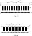
- the small hole has a diameter of 5 micrometers, its depth may need to be as large as 50 micrometers in order to make a collimation angle small enough.
- the collimator of such a thickness is generally difficult to be manufactured by a panel factory or a semiconductor factory; and if an optical fiber is used as the collimator, the cost will be increased and the cost of manufacturing the optical fiber will be very high.
- Embodiments of the present disclosure provide a collimator that includes at least two collimation layers and one or more light-transmissive substrates, each of which is arranged between two adjacent ones of the at least two collimation layers.
- the at least two collimation layers have a plurality of collimation holes, and the corresponding collimation holes of the two adjacent collimation layers are aligned holes, or the corresponding collimation holes of the two adjacent collimation layers are coupled to each other in a staggered manner.
- the two adjacent collimation layers have a same number of collimation holes, and the corresponding collimation holes of the two adjacent collimation layers are arranged opposite to each other.
- the at least two collimation layers are made of a light-shielding material.
- Embodiments of the present disclosure further provide an optical fingerprint reader that includes a cover plate, an optical sensor layer and the collimator as described above.
- the collimator is arranged between the cover plate and the optical sensor layer.
- the collimation holes of one of the at least two collimation layers closest to the optical sensor layer have a one-to-one relationship with sensor pixels of the optical sensor layer.
- the collimation holes of one of the at least two collimation layers closest to the optical sensor layer have a one-to-many relationship with sensor pixels of the optical sensor layer.
- the collimation holes of one of the at least two collimation layers closest to the optical sensor layer have a many-to-one relationship with sensor pixels of the optical sensor layer.
- Embodiments of the present disclosure further provide a full screen display that includes an organic light emitting diode (OLED) layer and the optical fingerprint reader as described above.
- OLED organic light emitting diode
- the OLED layer is arranged between the cover plate and the collimator, and the collimator and the optical sensor layer cover the entire OLED layer.
- the OLED layer is a flexible OLED layer or a glass OLED layer.
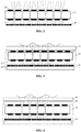
- FIG. 2 is a schematic structural diagram of a collimator provided in an embodiment 1 of the present disclosure.
- the collimator may specifically include at least two stacked collimation layers 21 and 22 and one or more light-transmissive substrates 23, each of which is arranged between two adjacent collimation layers.
- the at least two collimation layers 21, 22 have a plurality of collimation holes, and the corresponding collimation holes of two adjacent collimation layers 21, 22 are aligned holes, or are coupled to each other in a staggered manner, so as to collimate light emitted from a light source 24.
- the at least two collimation layers 21 and 22 are made of a light-shielding material.
- they are composed of a pure aluminum foil strip and a transparent polyester film strip.
- the light-transmissive substrate 23 is made of a light-transmissive material, such as glass and polymers.
- the collimation holes can have circular, regular hexagonal, triangular or other shapes, and they can be circular here, for example.
- the aligned holes may be at least two collimation holes whose axes are on a same straight line, and the aligned holes may be implemented in such a manner that the collimation layers 21, 22 are configured to have a same number of collimation holes which are distributed in a same manner and have a same size, and the corresponding collimation holes of the collimation layers 21 and 22 are arranged opposite to each other.
- the coupling of the corresponding collimation holes in the collimation layers 21 and 22 in the staggered manner may be implemented in such a manner that respective light receiving angles of the collimation holes in the two adjacent collimation layers 21 and 22 are calculated from thicknesses of the transparent substrate 23 and each of the collimation layers 21 and 22, and distribution positions, shapes, and sizes of the collimation holes in the collimation layers 21 and 22, and then the position of any one or more of the collimation layers 21 and 22 is customarily adjusted to realize the coupling of the collimation holes in the collimation layers 21 and 22 in the staggered manner.
- the staggering may be the staggering of two adjacent collimation layers, or may be a case where odd-numbered collimation layers exactly overlap in a stacking direction of the collimation layers and even-numbered collimation layers exactly overlap in the stacking direction; or, the collimation layers may be staggered on a group basis, and each group may include a variable number of collimation layers.
- the thicknesses of the collimation layers may not be identical.
- FIG. 2 shows a structure having only two collimation layers.
- a structure having three or more collimation layers it is not difficult to understand that if one collimation layer is added, a layer of a light-transmissive substrate will be added between the newly-added collimation layer and the collimation layer closest to the newly-added collimation layer.
- the coupling of the collimation holes in three or more collimation layers in a staggered manner is similar to that of the two collimation layers, and is not repeated here.
- a very thin layer of black material can be formed by, for example, a method for manufacturing a black matrix (BM) of a liquid crystal display (LCD).
- the BM process can achieve the application of a layer of material of about 2 micrometers, making it difficult to form deep and small holes, but it can be used to form a collimation effect similar to that of the deep and small holes by applying the material on both upper and lower sides of a transparent substrate, and the process is simple and cheap.
- the transparent substrate is provided to reduce the thickness required for the collimation layer, so as to further reduce the manufacturing cost while ensuring the collimation effect.
- this embodiment 2 further provides an illuminator which includes a light source configured to emit light and the collimator of the embodiment 1 configured to collimate the light emitted from the light source.
- a collimator can be placed between a lamp and a lampshade to control an irradiation angle of the electric lamp.
- a light output angle of the illuminator can be adjusted based on the collimation of the light by the collimator.
- FIG. 3 is a schematic structural diagram of an optical fingerprint reader provided in the embodiment 3 of the present disclosure.
- the optical fingerprint reader may specifically include a (protective) cover plate 31, an optical sensor layer 33, and the collimator 32 described in the embodiment 1.
- the collimator 32 is arranged between the cover plate 31 and the optical sensor layer 33, and configured to collimate light emitted from the optical sensor layer 33.
- the collimation holes of a collimation layer 321 of the at least two collimation layers in the collimator 32 closest to the optical sensor layer 33 may have a one-to-one, one-to-many, or many-to-one relationship with sensor pixels of the optical sensor layer 33.
- FIG. 3 it is not difficult to understand that how the correspondence between the collimation holes of the collimation layer 321 and the sensor pixels 331 is set can be determined based on actual needs of a user. Take FIG. 3 as an example, in which a plurality of sensor pixels 331 can be set to correspond to one collimation hole so that the optical sensor can collect enough optical signals, and a clearer fingerprint image can be thus obtained.
- the collimator based on the two layers of small holes in this embodiment collimates the light emitted by the optical sensor to avoid light leakage and achieve the purpose of accurately recognizing fingerprints.
- FIG. 4 is a schematic structural diagram of a full screen display provided in an embodiment 4 of the present disclosure.
- the full screen display may specifically include an OLED layer 42 and an optical fingerprint reader in the embodiment 3.
- the OLED layer 42 is arranged between the cover plate 41 and the collimator 43 (the collimation layers), and the collimator 43 and the optical sensor layer 44 cover the entire OLED layer 42.
- the OLED layer 42 is a flexible OLED layer or a glass OLED layer.
- a plastic OLED is a well-developed flexible OLED or glass OLED, and a cover glass 41 is placed above it and an optical sensor layer 44 and a collimator 43 are placed under the entire OLED module.
- the glass-based optical sensor layer may be an on/off thin film transistor (TFT) + photo TFT, or an on/off TFT + a photo diode (a positive intrinsic negative (PIN) photo diode).
- TFT thin film transistor
- PIN positive intrinsic negative
- the collimation holes can have a one-to-one relationship with the sensor pixels, that is, a fiber optic tube (an optical fiber collimator) corresponds to one pixel.
- the collimation holes may have a one-to-many or many-to-one relationship with the sensor pixels.
- this embodiment based on the above-mentioned collimator can allow the fingerprint recognition module to be arranged below the OLED layer 42 to achieve that fingerprint imaging can be clearly applied to a large-area glass-based image sensor without affecting or sacrificing the design or performance of the original OLED. It is thus possible to achieve the technology of full screen displays of mobile phones and pads, for example. Moreover, due to the low cost of the double-layered or multi-layered small-hole collimator structure, the production cost of the full screen display can be further reduced.
- the embodiments of the present disclosure may be provided as a method, a system, or a computer program product. Therefore, the present disclosure may take the form of an entirely hardware embodiment, an entirely software embodiment, or an embodiment combining software and hardware aspects. Moreover, the present disclosure may take the form of a computer program product implemented on one or more computer-usable storage media (including, but not limited to, a magnetic disk memory, a compact disk read-only memory (CD-ROM), an optical memory, etc.) containing computer-usable program codes therein.
- a computer-usable storage media including, but not limited to, a magnetic disk memory, a compact disk read-only memory (CD-ROM), an optical memory, etc.
Landscapes
- Engineering & Computer Science (AREA)
- Physics & Mathematics (AREA)
- General Physics & Mathematics (AREA)
- Human Computer Interaction (AREA)
- Multimedia (AREA)
- Theoretical Computer Science (AREA)
- Optics & Photonics (AREA)
- Electroluminescent Light Sources (AREA)
- Image Input (AREA)
Applications Claiming Priority (2)
| Application Number | Priority Date | Filing Date | Title |
|---|---|---|---|
| CN201711044121.6A CN107844767B (zh) | 2017-10-31 | 2017-10-31 | 一种准直器、光学指纹识别器以及全面屏 |
| PCT/CN2018/112408 WO2019085859A1 (zh) | 2017-10-31 | 2018-10-29 | 准直器、光学指纹识别器以及全面屏 |
Publications (2)
| Publication Number | Publication Date |
|---|---|
| EP3706033A1 true EP3706033A1 (de) | 2020-09-09 |
| EP3706033A4 EP3706033A4 (de) | 2020-12-30 |
Family
ID=61681162
Family Applications (1)
| Application Number | Title | Priority Date | Filing Date |
|---|---|---|---|
| EP18874564.0A Withdrawn EP3706033A4 (de) | 2017-10-31 | 2018-10-29 | Kollimator, optischer fingerabdruckerkenner und vollbildschirm |
Country Status (4)
| Country | Link |
|---|---|
| US (1) | US20200342195A1 (de) |
| EP (1) | EP3706033A4 (de) |
| CN (1) | CN107844767B (de) |
| WO (1) | WO2019085859A1 (de) |
Families Citing this family (26)
| Publication number | Priority date | Publication date | Assignee | Title |
|---|---|---|---|---|
| CN107844767B (zh) * | 2017-10-31 | 2020-03-17 | 维沃移动通信有限公司 | 一种准直器、光学指纹识别器以及全面屏 |
| CN110349984B (zh) | 2018-04-01 | 2021-08-03 | 广州印芯半导体技术有限公司 | 具有光学结构的集成电路 |
| CN108596080B (zh) * | 2018-04-20 | 2021-05-14 | Oppo广东移动通信有限公司 | 指纹识别组件、显示装置及电子装置 |
| CN108615003B (zh) * | 2018-04-20 | 2019-06-11 | Oppo广东移动通信有限公司 | 指纹识别组件、显示装置及电子装置 |
| PL3701420T3 (pl) | 2018-05-07 | 2021-11-08 | Wavetouch Limited | Kompaktowy czujnik optyczny do wykrywania linii papilarnych |
| CN110502955A (zh) * | 2018-05-17 | 2019-11-26 | 京东方科技集团股份有限公司 | 指纹识别面板、指纹识别方法及显示装置 |
| CN110175492B (zh) * | 2018-07-20 | 2022-03-01 | 神盾股份有限公司 | 光学指纹感测装置 |
| US10635374B2 (en) * | 2018-08-28 | 2020-04-28 | Innolux Corporation | Electronic device |
| US11922713B2 (en) | 2018-09-27 | 2024-03-05 | Apple Inc. | Under-display optical fingerprint sensor with NFV collimator and TFT/organic imager |
| CN109239938A (zh) * | 2018-10-11 | 2019-01-18 | 京东方科技集团股份有限公司 | 光学准直结构及其制作方法、指纹识别装置 |
| CN109643377A (zh) * | 2018-11-19 | 2019-04-16 | 深圳市汇顶科技股份有限公司 | 指纹识别装置和电子设备 |
| CN109753919B (zh) * | 2018-12-29 | 2021-04-02 | 武汉华星光电技术有限公司 | 光学指纹识别装置 |
| CN109740556B (zh) * | 2019-01-10 | 2021-02-02 | 京东方科技集团股份有限公司 | 基于准直光取出的光学结构的指纹识别模块及其制备方法 |
| CN111476055A (zh) * | 2019-01-23 | 2020-07-31 | 南昌欧菲生物识别技术有限公司 | 柔性准直器及其制备方法、指纹识别模组以及电子设备 |
| CN110309705B (zh) | 2019-04-30 | 2022-04-19 | 厦门天马微电子有限公司 | 显示面板和显示装置 |
| CN111914605A (zh) * | 2019-05-10 | 2020-11-10 | 南昌欧菲生物识别技术有限公司 | 准直器的制作方法、准直器、光学指纹模组及电子设备 |
| CN110278299B (zh) * | 2019-06-24 | 2021-10-19 | Oppo广东移动通信有限公司 | 显示装置、电子设备及图像获取方法 |
| CN110321832B (zh) * | 2019-06-28 | 2021-05-18 | 维沃移动通信有限公司 | 光学模组及移动终端 |
| CN112151572B (zh) * | 2019-06-28 | 2023-06-23 | 云谷(固安)科技有限公司 | 指纹识别显示器件及其制备方法、指纹识别显示装置 |
| CN112199979A (zh) * | 2019-07-07 | 2021-01-08 | 奕力科技股份有限公司 | 能够侦测一手指的指纹的显示装置与指纹识别芯片 |
| CN112766024A (zh) * | 2019-11-04 | 2021-05-07 | 上海箩箕技术有限公司 | 准直器、指纹识别装置及其指纹识别方法 |
| KR102383275B1 (ko) * | 2020-04-28 | 2022-04-08 | 베이징 샤오미 모바일 소프트웨어 컴퍼니 리미티드 난징 브랜치. | 단말 기기 |
| CN111785763A (zh) * | 2020-07-29 | 2020-10-16 | 北海惠科光电技术有限公司 | 一种显示面板及其制作方法 |
| CN112530999B (zh) | 2020-11-30 | 2022-10-25 | 厦门天马微电子有限公司 | 一种显示装置及其制作方法 |
| CN112816398B (zh) * | 2020-12-30 | 2023-07-25 | 中国科学院近代物理研究所 | 植物微束辐照实验准直器以及自动换样装置 |
| CN112861651B (zh) * | 2021-01-20 | 2024-06-28 | 京东方科技集团股份有限公司 | 显示面板和显示装置 |
Family Cites Families (11)
| Publication number | Priority date | Publication date | Assignee | Title |
|---|---|---|---|---|
| US10049256B2 (en) * | 2015-12-11 | 2018-08-14 | Gingy Technology Inc. | Fingerprint sensing module |
| US10732771B2 (en) * | 2014-11-12 | 2020-08-04 | Shenzhen GOODIX Technology Co., Ltd. | Fingerprint sensors having in-pixel optical sensors |
| US10181070B2 (en) * | 2015-02-02 | 2019-01-15 | Synaptics Incorporated | Low profile illumination in an optical fingerprint sensor |
| US9829614B2 (en) * | 2015-02-02 | 2017-11-28 | Synaptics Incorporated | Optical sensor using collimator |
| US10410037B2 (en) * | 2015-06-18 | 2019-09-10 | Shenzhen GOODIX Technology Co., Ltd. | Under-screen optical sensor module for on-screen fingerprint sensing implementing imaging lens, extra illumination or optical collimator array |
| US10176355B2 (en) * | 2015-12-03 | 2019-01-08 | Synaptics Incorporated | Optical sensor for integration in a display |
| KR102570180B1 (ko) * | 2016-11-28 | 2023-08-25 | 엘지디스플레이 주식회사 | 지문 센서 일체형 전계 발광 표시장치 |
| CN206470779U (zh) * | 2016-12-23 | 2017-09-05 | 敦捷光电股份有限公司 | 生物特征辨识装置 |
| CN106773219B (zh) * | 2017-02-07 | 2019-11-05 | 京东方科技集团股份有限公司 | 一种显示装置 |
| CN106873063B (zh) * | 2017-02-23 | 2018-09-18 | 京东方科技集团股份有限公司 | 一种显示装置 |
| CN107844767B (zh) * | 2017-10-31 | 2020-03-17 | 维沃移动通信有限公司 | 一种准直器、光学指纹识别器以及全面屏 |
-
2017
- 2017-10-31 CN CN201711044121.6A patent/CN107844767B/zh active Active
-
2018
- 2018-10-29 WO PCT/CN2018/112408 patent/WO2019085859A1/zh not_active Ceased
- 2018-10-29 EP EP18874564.0A patent/EP3706033A4/de not_active Withdrawn
- 2018-10-29 US US16/757,969 patent/US20200342195A1/en not_active Abandoned
Also Published As
| Publication number | Publication date |
|---|---|
| WO2019085859A1 (zh) | 2019-05-09 |
| US20200342195A1 (en) | 2020-10-29 |
| CN107844767A (zh) | 2018-03-27 |
| EP3706033A4 (de) | 2020-12-30 |
| CN107844767B (zh) | 2020-03-17 |
Similar Documents
| Publication | Publication Date | Title |
|---|---|---|
| EP3706033A1 (de) | Kollimator, optischer fingerabdruckerkenner und vollbildschirm | |
| CN109716352B (zh) | 液晶显示指纹模组、屏下指纹识别系统及电子设备 | |
| US10664680B2 (en) | Optical fingerprint recognition apparatus and display panel | |
| US11106888B2 (en) | Display device for fingerprint identification and control method thereof | |
| CN107168465B (zh) | 显示模组及显示装置 | |
| EP3819898B1 (de) | Anzeigeschirm und endgerät | |
| US10324299B2 (en) | Video wall display device | |
| US9086761B2 (en) | Display apparatus | |
| CN106159105B (zh) | 光学膜结构与显示器结构 | |
| TWI569237B (zh) | 顯示裝置 | |
| US10782508B2 (en) | Imaging apparatus including an optical assembly for refracting ambient lights to bypass shielding members in display panel and method for producing the same and mobile terminal device | |
| US20150092442A1 (en) | Display, display assembly, and backlight module | |
| KR20170037773A (ko) | 광섬유를 포함하는 판상 광학부재 및 그를 포함하는 다중 패널 표시장치 | |
| US10151948B2 (en) | Display apparatus | |
| US12279505B2 (en) | Display device and touch controller | |
| JP2021532386A (ja) | 表示モジュール及び表示装置 | |
| WO2020133479A1 (zh) | 光学指纹识别模组及电子设备 | |
| JP2007264393A (ja) | 液晶表示装置 | |
| CN209486694U (zh) | 光学指纹识别模组及电子设备 | |
| US20220139104A1 (en) | Screen Assembly and Electronic Device | |
| CN108845460A (zh) | 一种背光模组及显示装置 | |
| CN106483713A (zh) | 背光模块 | |
| WO2025227774A1 (zh) | 电子设备和导光结构 | |
| CN213092333U (zh) | 电子装置 | |
| US9927629B2 (en) | Display apparatus and display system |
Legal Events
| Date | Code | Title | Description |
|---|---|---|---|
| STAA | Information on the status of an ep patent application or granted ep patent |
Free format text: STATUS: THE INTERNATIONAL PUBLICATION HAS BEEN MADE |
|
| PUAI | Public reference made under article 153(3) epc to a published international application that has entered the european phase |
Free format text: ORIGINAL CODE: 0009012 |
|
| STAA | Information on the status of an ep patent application or granted ep patent |
Free format text: STATUS: REQUEST FOR EXAMINATION WAS MADE |
|
| 17P | Request for examination filed |
Effective date: 20200422 |
|
| AK | Designated contracting states |
Kind code of ref document: A1 Designated state(s): AL AT BE BG CH CY CZ DE DK EE ES FI FR GB GR HR HU IE IS IT LI LT LU LV MC MK MT NL NO PL PT RO RS SE SI SK SM TR |
|
| AX | Request for extension of the european patent |
Extension state: BA ME |
|
| A4 | Supplementary search report drawn up and despatched |
Effective date: 20201130 |
|
| RIC1 | Information provided on ipc code assigned before grant |
Ipc: G06K 9/00 20060101AFI20201124BHEP Ipc: G02B 27/30 20060101ALI20201124BHEP |
|
| DAV | Request for validation of the european patent (deleted) | ||
| DAX | Request for extension of the european patent (deleted) | ||
| STAA | Information on the status of an ep patent application or granted ep patent |
Free format text: STATUS: EXAMINATION IS IN PROGRESS |
|
| 17Q | First examination report despatched |
Effective date: 20220909 |
|
| STAA | Information on the status of an ep patent application or granted ep patent |
Free format text: STATUS: THE APPLICATION HAS BEEN WITHDRAWN |
|
| 18W | Application withdrawn |
Effective date: 20240606 |