EP3705839B1 - Improved signal conditioning circuit for use with active magnetic bearings - Google Patents
Improved signal conditioning circuit for use with active magnetic bearings Download PDFInfo
- Publication number
- EP3705839B1 EP3705839B1 EP20161656.2A EP20161656A EP3705839B1 EP 3705839 B1 EP3705839 B1 EP 3705839B1 EP 20161656 A EP20161656 A EP 20161656A EP 3705839 B1 EP3705839 B1 EP 3705839B1
- Authority
- EP
- European Patent Office
- Prior art keywords
- signal
- inductive
- sensing
- circuit
- sets
- Prior art date
- Legal status (The legal status is an assumption and is not a legal conclusion. Google has not performed a legal analysis and makes no representation as to the accuracy of the status listed.)
- Active
Links
Images






Classifications
-
- G—PHYSICS
- G01—MEASURING; TESTING
- G01D—MEASURING NOT SPECIALLY ADAPTED FOR A SPECIFIC VARIABLE; ARRANGEMENTS FOR MEASURING TWO OR MORE VARIABLES NOT COVERED IN A SINGLE OTHER SUBCLASS; TARIFF METERING APPARATUS; MEASURING OR TESTING NOT OTHERWISE PROVIDED FOR
- G01D5/00—Mechanical means for transferring the output of a sensing member; Means for converting the output of a sensing member to another variable where the form or nature of the sensing member does not constrain the means for converting; Transducers not specially adapted for a specific variable
- G01D5/12—Mechanical means for transferring the output of a sensing member; Means for converting the output of a sensing member to another variable where the form or nature of the sensing member does not constrain the means for converting; Transducers not specially adapted for a specific variable using electric or magnetic means
- G01D5/14—Mechanical means for transferring the output of a sensing member; Means for converting the output of a sensing member to another variable where the form or nature of the sensing member does not constrain the means for converting; Transducers not specially adapted for a specific variable using electric or magnetic means influencing the magnitude of a current or voltage
- G01D5/20—Mechanical means for transferring the output of a sensing member; Means for converting the output of a sensing member to another variable where the form or nature of the sensing member does not constrain the means for converting; Transducers not specially adapted for a specific variable using electric or magnetic means influencing the magnitude of a current or voltage by varying inductance, e.g. by a movable armature
-
- G—PHYSICS
- G01—MEASURING; TESTING
- G01D—MEASURING NOT SPECIALLY ADAPTED FOR A SPECIFIC VARIABLE; ARRANGEMENTS FOR MEASURING TWO OR MORE VARIABLES NOT COVERED IN A SINGLE OTHER SUBCLASS; TARIFF METERING APPARATUS; MEASURING OR TESTING NOT OTHERWISE PROVIDED FOR
- G01D5/00—Mechanical means for transferring the output of a sensing member; Means for converting the output of a sensing member to another variable where the form or nature of the sensing member does not constrain the means for converting; Transducers not specially adapted for a specific variable
- G01D5/12—Mechanical means for transferring the output of a sensing member; Means for converting the output of a sensing member to another variable where the form or nature of the sensing member does not constrain the means for converting; Transducers not specially adapted for a specific variable using electric or magnetic means
- G01D5/14—Mechanical means for transferring the output of a sensing member; Means for converting the output of a sensing member to another variable where the form or nature of the sensing member does not constrain the means for converting; Transducers not specially adapted for a specific variable using electric or magnetic means influencing the magnitude of a current or voltage
- G01D5/20—Mechanical means for transferring the output of a sensing member; Means for converting the output of a sensing member to another variable where the form or nature of the sensing member does not constrain the means for converting; Transducers not specially adapted for a specific variable using electric or magnetic means influencing the magnitude of a current or voltage by varying inductance, e.g. by a movable armature
- G01D5/22—Mechanical means for transferring the output of a sensing member; Means for converting the output of a sensing member to another variable where the form or nature of the sensing member does not constrain the means for converting; Transducers not specially adapted for a specific variable using electric or magnetic means influencing the magnitude of a current or voltage by varying inductance, e.g. by a movable armature differentially influencing two coils
-
- G—PHYSICS
- G01—MEASURING; TESTING
- G01B—MEASURING LENGTH, THICKNESS OR SIMILAR LINEAR DIMENSIONS; MEASURING ANGLES; MEASURING AREAS; MEASURING IRREGULARITIES OF SURFACES OR CONTOURS
- G01B7/00—Measuring arrangements characterised by the use of electric or magnetic techniques
- G01B7/003—Measuring arrangements characterised by the use of electric or magnetic techniques for measuring position, not involving coordinate determination
-
- G—PHYSICS
- G01—MEASURING; TESTING
- G01B—MEASURING LENGTH, THICKNESS OR SIMILAR LINEAR DIMENSIONS; MEASURING ANGLES; MEASURING AREAS; MEASURING IRREGULARITIES OF SURFACES OR CONTOURS
- G01B7/00—Measuring arrangements characterised by the use of electric or magnetic techniques
- G01B7/02—Measuring arrangements characterised by the use of electric or magnetic techniques for measuring length, width or thickness
- G01B7/023—Measuring arrangements characterised by the use of electric or magnetic techniques for measuring length, width or thickness for measuring distance between sensor and object
-
- F—MECHANICAL ENGINEERING; LIGHTING; HEATING; WEAPONS; BLASTING
- F16—ENGINEERING ELEMENTS AND UNITS; GENERAL MEASURES FOR PRODUCING AND MAINTAINING EFFECTIVE FUNCTIONING OF MACHINES OR INSTALLATIONS; THERMAL INSULATION IN GENERAL
- F16C—SHAFTS; FLEXIBLE SHAFTS; ELEMENTS OR CRANKSHAFT MECHANISMS; ROTARY BODIES OTHER THAN GEARING ELEMENTS; BEARINGS
- F16C32/00—Bearings not otherwise provided for
- F16C32/04—Bearings not otherwise provided for using magnetic or electric supporting means
- F16C32/0406—Magnetic bearings
- F16C32/044—Active magnetic bearings
- F16C32/0444—Details of devices to control the actuation of the electromagnets
- F16C32/0446—Determination of the actual position of the moving member, e.g. details of sensors
-
- F—MECHANICAL ENGINEERING; LIGHTING; HEATING; WEAPONS; BLASTING
- F16—ENGINEERING ELEMENTS AND UNITS; GENERAL MEASURES FOR PRODUCING AND MAINTAINING EFFECTIVE FUNCTIONING OF MACHINES OR INSTALLATIONS; THERMAL INSULATION IN GENERAL
- F16C—SHAFTS; FLEXIBLE SHAFTS; ELEMENTS OR CRANKSHAFT MECHANISMS; ROTARY BODIES OTHER THAN GEARING ELEMENTS; BEARINGS
- F16C32/00—Bearings not otherwise provided for
- F16C32/04—Bearings not otherwise provided for using magnetic or electric supporting means
- F16C32/0406—Magnetic bearings
- F16C32/044—Active magnetic bearings
- F16C32/0474—Active magnetic bearings for rotary movement
-
- G—PHYSICS
- G01—MEASURING; TESTING
- G01B—MEASURING LENGTH, THICKNESS OR SIMILAR LINEAR DIMENSIONS; MEASURING ANGLES; MEASURING AREAS; MEASURING IRREGULARITIES OF SURFACES OR CONTOURS
- G01B7/00—Measuring arrangements characterised by the use of electric or magnetic techniques
- G01B7/02—Measuring arrangements characterised by the use of electric or magnetic techniques for measuring length, width or thickness
-
- G—PHYSICS
- G01—MEASURING; TESTING
- G01B—MEASURING LENGTH, THICKNESS OR SIMILAR LINEAR DIMENSIONS; MEASURING ANGLES; MEASURING AREAS; MEASURING IRREGULARITIES OF SURFACES OR CONTOURS
- G01B7/00—Measuring arrangements characterised by the use of electric or magnetic techniques
- G01B7/14—Measuring arrangements characterised by the use of electric or magnetic techniques for measuring distance or clearance between spaced objects or spaced apertures
- G01B7/144—Measuring play on bearings
-
- G—PHYSICS
- G01—MEASURING; TESTING
- G01D—MEASURING NOT SPECIALLY ADAPTED FOR A SPECIFIC VARIABLE; ARRANGEMENTS FOR MEASURING TWO OR MORE VARIABLES NOT COVERED IN A SINGLE OTHER SUBCLASS; TARIFF METERING APPARATUS; MEASURING OR TESTING NOT OTHERWISE PROVIDED FOR
- G01D11/00—Component parts of measuring arrangements not specially adapted for a specific variable
- G01D11/02—Bearings or suspensions for moving parts
-
- G—PHYSICS
- G01—MEASURING; TESTING
- G01D—MEASURING NOT SPECIALLY ADAPTED FOR A SPECIFIC VARIABLE; ARRANGEMENTS FOR MEASURING TWO OR MORE VARIABLES NOT COVERED IN A SINGLE OTHER SUBCLASS; TARIFF METERING APPARATUS; MEASURING OR TESTING NOT OTHERWISE PROVIDED FOR
- G01D5/00—Mechanical means for transferring the output of a sensing member; Means for converting the output of a sensing member to another variable where the form or nature of the sensing member does not constrain the means for converting; Transducers not specially adapted for a specific variable
- G01D5/54—Mechanical means for transferring the output of a sensing member; Means for converting the output of a sensing member to another variable where the form or nature of the sensing member does not constrain the means for converting; Transducers not specially adapted for a specific variable using means specified in two or more of groups G01D5/02, G01D5/12, G01D5/26, G01D5/42, and G01D5/48
- G01D5/56—Mechanical means for transferring the output of a sensing member; Means for converting the output of a sensing member to another variable where the form or nature of the sensing member does not constrain the means for converting; Transducers not specially adapted for a specific variable using means specified in two or more of groups G01D5/02, G01D5/12, G01D5/26, G01D5/42, and G01D5/48 using electric or magnetic means
-
- F—MECHANICAL ENGINEERING; LIGHTING; HEATING; WEAPONS; BLASTING
- F16—ENGINEERING ELEMENTS AND UNITS; GENERAL MEASURES FOR PRODUCING AND MAINTAINING EFFECTIVE FUNCTIONING OF MACHINES OR INSTALLATIONS; THERMAL INSULATION IN GENERAL
- F16C—SHAFTS; FLEXIBLE SHAFTS; ELEMENTS OR CRANKSHAFT MECHANISMS; ROTARY BODIES OTHER THAN GEARING ELEMENTS; BEARINGS
- F16C2233/00—Monitoring condition, e.g. temperature, load, vibration
Definitions
- the present invention relates to the field of electronics in general.
- the invention relates to an improved signal conditioning circuit for use with active magnetic bearings.
- Active magnetic bearings for supporting a rotor traditionally comprise electromagnets with variable excitation controlled by displacement sensors using electronic servo circuits.
- the displacement sensors are sensitive to changes in the position of the rotor relative to a reference position.
- the displacement sensors may be of the optical, capacitive, eddy current or inductive type.
- An inductive position sensor comprises a set of inductive elements with a variable gap fixed to the stator and cooperating with a reference ring, or 'target', integral with the rotor.
- the reference ring traditionally comprises a ring composed of magnetic sheets or made of ferrite.
- the reference ring must be manufactured with great care, as manufacturing defects and build tolerances limit the performance of the inductive sensor elements.
- Bridge type inductive position sensors used for magnetic bearing applications traditionally use a phase sensitive (synchronous) de-modulation circuit implemented using analogue electronics.
- the phase of the reference waveform should be adjusted to match the phase of the output signal from the sensor when the rotor is displaced from the centre position.
- this phase shifting is traditionally performed using RC filter networks which are matched when the system is in its final installation with the field cabling installed.
- Document US 3,650,581 discloses a mechanical contact-free bearing system for a rotor comprising a magnetic system which includes at least one carrier magnet for suspending the rotor with its axis vertical.
- Document GB 1 500 809 discloses a radial active magnetic bearing having a rotating drive and comprising in combination one or more stators and a rotor associated with an air gap detected by sensors, a control rotating field being superimposed upon a drive rotating field produced by the stator winding as a result of energization by three-phase AC.
- Document EP 2 781 887 discloses a variable inductance type position sensor system comprising a rotary target of ferromagnetic material fixed on a rotary shaft and a stationary magnetic circuit which is placed around the rotor target.
- Document US 2014/252899 discloses a rotating electrical machine including a stator, a rotor, and at least one active magnetic bearing including a bearing winding, which is an air-gap winding, and includes at least a first phase winding and a second phase winding.
- the present invention provides an inductive sensing circuit comprising: a signal generator, configured to generate a drive signal; one or more sensing arrangements, each of the one or more sensing arrangements comprising: two sets of one or more inductive sensing elements configured in a half bridge arrangement, the two sets of one or more inductive sensing elements driven by the drive signal; a correction signal circuit configured to generate a correction signal, wherein the correction signal is an adjustably scaled version of the drive signal; and a summing circuit configured to sum an output signal of the two sets of one or more inductive sensing elements with the correction signal; and a demodulation circuit, configured to demodulate an output of the summing circuit of each of the one or more sensing arrangements.
- the present invention also provides a method for correcting an output signal of two sets of one or more inductive sensor elements, the method comprising: generating a drive signal; driving the two sets of one or more inductive sensor elements by applying the drive signal; generating a correction signal, wherein the correction signal is an adjustably scaled copy of the drive signal; summing the output signal of the two sets of one or more inductive sensor elements with the correction signal; and demodulating the summed signal.
- the present invention also provides an active magnetic bearing comprising the inductive sensing circuit disclosed herein.
- Embodiments of the invention disclosed herein provide inductive position sensing apparatus and methods which are tolerant to errors from manufacturing tolerances of the reference ring or inductive sensor elements, but are also tolerant to mismatches in the impedance of opposed inductive sensing elements.
- inductive sensor elements may not be a singular inductive sensor element, but instead may be one or more inductive sensor elements in a series arrangement.
- Figure 1 shows a high level block diagram of a typical radial inductive position sensor arrangement. Typically, synchronous de-modulation of the "in-phase" component of the signal is used to remove noise and/or interfering signals from the sensor outputs.
- Figure 1 shows a plurality of inductive sensor elements 132a, 132b, 134a, and 134b, arranged around the circumference of rotor 102. Inductive sensor elements 132a and 132b form a first pair. Inductive sensor elements 134a and 134b form a second pair. First pair of inductive sensor elements 132a and 132b are circumferentially arranged diametrically opposite each other with respect to the axis of rotation of the rotor 102.
- a signal generator 110 is configured to generate a sinusoidal drive signal 112. In some embodiments the drive signal may be non-sinusoidal and could be, for example, a square wave. Signal generator 110 is operably coupled to a balanced voltage drive 120. Signal generator 110 also provides a synchronisation signal to first and second synchronous de-modulation circuitry 152 and 154. This synchronisation signal may provide one input to a convolution algorithm used to perform synchronous de-modulation at the first and second synchronous de-modulation circuitry 152 and 154.
- First pair of inductive sensor elements 132a and 132b is connected in a first half bridge arrangement.
- Second pair of inductive sensor elements 134a and 134b is connected in a second half bridge arrangement.
- a first output 122 of balanced voltage drive 120 is coupled to a first input of each of the first and second half bridge arrangements.
- a second output 124 of balanced voltage drive 120 is coupled to a second input of each of the first and second half bridge arrangements.
- balanced voltage drive 120 may include circuitry configured to amplify the sinusoidal drive signal 122 from the signal generator 110.
- An output 142 from the first half bridge arrangement is operably coupled to a first input of first optional signal conditioning circuitry 180.
- a first output 142' of first optional signal conditioning circuitry 180 is coupled to a first input of second synchronous de-modulation circuitry 154.
- An output 144 from the second half bridge arrangement is operably coupled to a second input of first optional signal conditioning circuitry 180.
- a second output 144' of first optional signal conditioning circuitry 180 is coupled to a second input of second synchronous de-modulation circuitry 154.
- Second synchronous de-modulation circuitry 154 is configured to remove noise and/or interfering signals from each of outputs 142' and 144' of the first (132a, 132b) and second (134a, 134b) half bridge inductive sensor element arrangements or optional signal conditioning circuitry 180 such that only the respective sensor output remains (i.e. the signal which indicates the position of the rotor 102 along a particular axis).
- Element 158 converts a copy of outputs 122 and 124 (one or both) of balanced voltage drive 120 into a single ended signal 159.
- Single ended signal 159 from element 158 is operably coupled to an input of second optional signal conditioning circuitry 181.
- An output 159' of second optional signal conditioning circuitry 181 is coupled to an input of first synchronous de-modulation circuitry 152.
- First synchronous de-modulation circuitry 152 is configured to remove noise and/or interfering signals from single ended signal 159.
- First and second outputs 162 and 164 of second synchronous de-modulation circuitry 154 are operably coupled to first and second inputs of ratiometric block 156.
- Output 166 of first synchronous de-modulation circuitry 152 is operably coupled to a third input of ratiometric block 156.
- first and second synchronous de-modulation circuitry 152 and 154 are illustrated as separate blocks in Figure 1 , they may be implemented as a single circuit or as two or more separate circuits.
- first and second optional signal conditioning circuitry 180 and 181 may be implemented as a single circuit or as multiple independent circuits.
- Ratiometric block 156 is configured to convert sensor signals 162 and 164 to a meaningful output signal for use in controlling the actuators and/or electromagnets of an Active Magnetic Bearing.
- Signal 166 is used as a reference signal in converting signals 162 and 164, in order to eliminate any effect caused by variation in the outputs of balanced voltage drive 120. Synchronous de-modulation can be performed using either analogue implementations or digital implementations.
- inductive sensor elements 132a, 132b, 134a and 134b may be spaced equidistant about the circumference of rotor 102 (i.e. 90 degrees between each of inductive sensor elements 132a, 132b, 134a and 134b). In some embodiments, the spacing between the inductive sensor elements 132a, 132b, 134a and 134b may not be equal. However, inductive sensor elements 132a and 132b may still be diametrically opposed, and inductive sensor elements 134a and 134b may still be diametrically opposed.
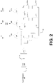
- Figure 2 shows a typical sensor design for use with digital implementations of synchronous de-modulation of the inductive position sensor element output signals.
- the circuit of Figure 2 provides an implementation of the elements of Figure 1 inside box 170.
- Figure 2 shows a signal generator 110, which is used to generate a sinusoidal drive signal 112 at a required frequency.
- signal generator 110 generates the signal digitally, however alternative embodiments may instead use an analogue signal generating stage.
- the signal generator 110 is operably coupled to a Digital-to-Analogue Converter (DAC) 212.
- DAC Digital-to-Analogue Converter
- AC Alternating Current
- AC couple 214 is configured to eliminate any Direct Current (DC) component of the sinusoidal drive signal 112.
- the AC couple 214 may be, for example, a suitably sized capacitor.
- the output of AC couple 214 is operably coupled to a power amplifier 216.
- Power amplifier 216 is coupled to balanced voltage drive 120.
- the balanced voltage drive 120 is implemented using a transformer with multiple secondary windings, however in other embodiments alternative means of implementing a balanced voltage drive may be used.
- a reference signal from balanced voltage drive 120 is coupled to amplifier 240, in order to provide a reference signal for performing the ratiometric function of ratiometric block 156.
- a first output 122 of balanced voltage drive 120 is coupled to a first input of each of the first (132a, 132b) and second (134a, 134b) half bridge inductive sensor element arrangements.
- a second output 124 of balanced voltage drive 120 is coupled to a second input of each of the first (132a, 132b) and second (134a, 134b) half bridge inductive sensor element arrangements.
- the sensed signal 142 from first pair of inductive sensor elements 132a, 132b is coupled to amplifier 242.
- the sensed signal from second pair of inductive sensor elements 134a, 134b is coupled to amplifier 244.
- amplifier stages 240, 242 and 244 may have adjustable gain.
- the respective outputs 241, 243 and 245 of amplifier stages 240, 242 and 244 are each coupled to the inputs of one or more Analogue-to-Digital Converters (ADC) 250.
- Analogue-to-Digital Converter(s) 250 are configured to convert analogue signals 241, 243 and 245 to digital signals 159', 142' and 144' respectively.
- Output 159' of Analogue-to-Digital Converter 250 is coupled to an input of first synchronous de-modulation circuitry 152 of Figure 1 .
- Outputs 142' and 144' of Analogue-to-Digital Converter 250 are coupled to first and second outputs of second synchronous de-modulation circuitry 154 of Figure 1 .
- Amplifier stages 240, 242 and 244 and Analogue-to-Digital Converter 250 may correspond to signal conditioning elements 180 and 181 of Figure 1 .
- First and second synchronous de-modulation circuitry 152 and 154 are coupled to ratiometric block 156 in the same manner as in Figure 1 .
- synchronous demodulation circuitry 152 and 154, and/or ratiometric block 156 are implemented digitally.
- Some digital implementations of the synchronous de-modulation circuitry 152 and 154, and ratiometric block 156 may combine Field Programmable Gate Arrays (FPGAs) or other control logic to handle the phase shifting and multiplication functions used for performing synchronous demodulation, and Digital Signal Processors (DSPs) or other control processing to handle the ratiometric function.
- the DSPs may also be used to perform Active Magnetic Bearing servo control functions.
- digital synchronous de-modulation of the output signal may comprise a programable signal generator 110 used to construct a sinusoidal drive signal 112 at a required frequency.
- the signal generator 110 may be configured to output a synchronising pulse for use by the first and second synchronous de-modulation circuitry 152 and 154, and/or ratiometric block 156.
- the signal generator 110 may be under the control of a supervisory FPGA or other control logic which may also be responsible for data communications and/or a supervisory state machine or other control logic which controls the sequencing of an overall Active Magnetic Bearing control system, which may include actuator elements or electromagnetic elements.
- Each Active Magnetic Bearing for use in a given installation may have its own control logic and/or processing, or control logic and/or processing may be shared between multiple Active Magnetic Bearings in a given installation.
- Motion of a rotor 102 supported by an Active Magnetic Bearing system may be typically constrained by mechanical "touchdown bearings" (one at each end of the rotor 102). These will normally be operational with a clearance, but when the rotor moves out of position the rotor may contact the touchdown bearings.
- the Active Magnetic Bearing system will normally be configured with the "centre" position defined by the mechanical centre of the touchdown bearing clearances, as opposed to the mechanical centre of the sensor clearances or the mechanical centre of the actuator clearances.
- Figure 3 shows a sinusoidal drive signal waveform 310 (which may be, for example, sinusoidal drive signal 112 generated by signal generator 110 of Figure 1 or Figure 2 ), and the ideal output signal of a half bridge inductive sensor element arrangement (which may be, for example, either half bridge inductive sensor element arrangement 132a, 132b; or half bridge inductive sensor element arrangement 134a, 134b) as the rotor 102 traverses (in one axis of motion) from contacting the touchdown bearings on one side (waveform 320), through the mechanical centre position (waveform 324) to contacting the touchdown bearings on the opposite side (waveform 322), for an ideal system.
- a half bridge inductive sensor element arrangement which may be, for example, either half bridge inductive sensor element arrangement 132a, 132b; or half bridge inductive sensor element arrangement 134a, 134b
- the input gain on the Analogue-to-Digital Converter 250 may be set to optimise the usage of the available Analogue-to-Digital Converter 250 input range for the allowable range of motion (between contacting the touchdown bearings on one side and contacting the touchdown bearings on the other side). This is done in order to maximise signal to noise ratio and minimise the effects of quantisation noise (i.e. noise caused by the error between the real analogue value of the signal input to the ADC 250 and the sampled output value associated with the input signal). Similar input range considerations apply for analogue implementations of the synchronous de-modulation circuit and ratiometric block.
- the mechanical centre of the half bridge inductive sensor element arrangement may be offset from the mechanical centre of the touchdown bearings (i.e. a misalignment between mechanical centre of the half bridge inductive sensor element arrangement and the mechanical centre of the touchdown bearings).
- the output signal of the sensor as the rotor 102 traverses (in one axis of motion) from contacting the touchdown bearings on one side (waveform 420), through the mechanical centre position of the touchdown bearings (waveform 424) to contacting the touchdown bearings on the opposite side (waveform 422) could be, for example, as shown in Figure 4 .
- the inductive sensor elements may not be perfectly matched, resulting in the null (minimum) output from the half bridge inductive sensor element arrangement being offset from the mechanical centre of the half bridge arrangement. This null is referred to as the electrical centre of the half bridge inductive sensor element arrangement.
- the input gain for the Analogue-to-Digital Converter 250 may be set so that the largest signal (for example, with amplitude 3A in Figure 4 , where A is an arbitrary value representing the amplitude of the signal) observed when traversing the rotor 102 can be correctly sampled by the Analogue-to-Digital Converter 250 (or the front end of the analogue circuit where the synchronous de-modulation is implemented using analogue components).
- the effect of this would be to reduce the sensitivity at the input of the synchronous demodulation circuit 152, 154 (or Analogue-to-Digital Converter 250) by a factor of 1/3, with a corresponding decrease in signal to noise ratio.
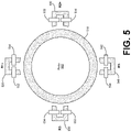
- Figure 5 shows an example of a typical construction of a radial inductive sensor arrangement used within an Active Magnetic Bearing system, as per Figure 1 .
- Figure 5 shows rotor shaft 502, with laminated reference ring 510.
- Inductive sensor element R1+ has laminated core 520 and coils 522 and 524.
- Inductive sensor element R2+ has laminated core 530 and coils 532 and 534.
- Inductive sensor element R1- has laminated core 540 and coils 542 and 544.
- Inductive sensor element R2- has laminated core 550 and coils 552 and 554.
- Inductive sensor element R1+ is arranged diametrically opposite inductive sensor element R1-.
- Inductive sensor element R2+ is arranged diametrically opposite inductive sensor element R2-.
- Inductive sensor elements R1+ and R1- are electrically connected in a first half bridge arrangement.
- Inductive sensor elements R2+ and R2- are electrically connected in a second half bridge arrangement.
- Figure 5 does not show any of the actuator parts or the touchdown bearings of an Active Magnetic Bearing system, and merely serves to illustrate one example arrangement of sensor elements.
- Figure 6 shows an example of a typical construction of an axial inductive slip sensor arrangement used within an Active Magnetic Bearing system, which may be used to detect the position of the rotor along the rotor axis.
- the inductive sensor is formed of pairs of opposed inductive sensor elements each wired to form a half bridge arrangement, and arranged along the axis of the rotor.
- Figure 6 shows a core shaft or rotor 602 with laminated reference ring 610.
- Laminated reference ring 610 may be supported by non-active mechanical support parts 612 and 614, which may be constructed from a non-magnetic material.
- Non-active mechanical support parts 612 and 614 may serve to keep the laminations of laminated reference ring 610 compressed. Non-active mechanical support parts 612 and 614 may also provide a boundary between the magnetic material of laminated reference ring 610 and non-active mechanical support parts 612 and 614.
- Inductive sensing elements 620 and 640 (which may alternatively be referred to as axial sensor rings) together form one element of a half bridge arrangement. Sensing elements 630 and 650 together form the other element of the half bridge arrangement.
- Figure 6 does not show any of the actuator parts or the touchdown bearings of an Active Magnetic Bearing system, and merely serves to illustrate one example arrangement of sensor elements.
- Figure 7 shows an alternative example of a typical construction of an axial inductive sensor arrangement using a disk as the target.
- Figure 7 shows a rotor 702 with a solid ferrite disc or laminated reference ring 710.
- Inductive sensing elements 720 and 740 together form one element of a half bridge arrangement.
- Inductive sensing elements 730 and 750 form the other element of the half bridge arrangement.
- Figure 7 does not show any of the actuator parts or the touchdown bearings of an Active Magnetic Bearing system, and merely serves to illustrate one example arrangement of sensor elements.
- An improved signal conditioning circuit disclosed herein provides the addition of a controlled amount of the sinusoidal drive signal used within the drive circuit to the signals output by the half bridge inductive sensor element arrangements (132a, 132b; 134a, 134b).
- the added signal will be of a controlled amplitude and for a particular axis, and may be of either positive or negative phase depending on the required correction for the particular half bridge sensor element arrangement.
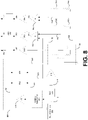
- Figure 8 shows a schematic of an improved sensor and signal conditioning circuit design in accordance with embodiments of the disclosure.
- the improved signal conditioning circuit of Figure 8 is an improved version of the signal conditioning circuit of Figure 2 . Accordingly, the same reference numerals are used to indicate elements which are the same as those in Figure 2 .
- Figure 8 shows signal generator 110 used to generate a sinusoidal drive signal at a required frequency. Signal generator 110 is coupled by connection 811 to supply a copy of drive signal 112 to a negative gain circuitry 820 (which may be alternatively referred to as an inverting amplifier, which may or may not have unity gain), and to a first input of each of first and second correction signal adjustment means 832 and 834 (where correction signal adjustment means 832 and 834 may be, for example, a potentiometer).
- a negative gain circuitry 820 which may be alternatively referred to as an inverting amplifier, which may or may not have unity gain
- correction signal adjustment means 832 and 834 may be, for example, a potentiometer
- Negative gain circuitry 820 is configured to generate a copy of drive signal 112 with an inverted polarity.
- An output of negative gain circuitry 820 is coupled by connection 821 to a second input of each of first and second correction signal adjustment potentiometers 832 and 834.
- First and second correction signal adjustment potentiometers 832 and 834 are each operable to scale a first and second correction signal by adjusting the amplitude and/or polarity of the signals at 811 and 821.
- the first correction signal output 833 of first correction signal adjustment potentiometer 832 is summed with the sensed signal 142 from first pair of inductive sensor elements 132a, 132b at summing block 842.
- the second correction signal output 835 of second correction signal adjustment potentiometer 834 is summed with the sensed signal 144 from the second pair of inductive sensor elements 134a, 134b at summing block 844.
- the outputs 843 and 845 of summing blocks 842 and 844 respectively are amplified by amplifier stages 242 and 244, respectively.
- the outputs 241, 243 and 245 of amplifier stages 240, 242 and 244 respectively are coupled to the inputs of one or more Analogue-to-Digital Converters (ADC) 250.
- ADC Analogue-to-Digital Converters
- the elements within block 801 may collectively be referred to as signal correction circuitry 801.
- first and second correction signals 833 and 835 may be isolated from signal generator 110 by use of a transformer 810 or other such isolating means in order to reduce the effect of ground noise on first and second correction signals 833 and 835.
- a separate isolation means may be used for each of correction signals 833 and 835.
- first and second correction signals 833 and 835 is shown as being controlled by first and second correction signal adjustment potentiometers 832 and 834, however scaling of the correction signals may alternatively be implemented using a range of techniques including: potentiometers, digitally controlled potentiometers, selected fixed resistors, etc. These techniques are intended to be non-limiting examples only.
- Figure 8 provides an inductive sensor element arrangement and signal conditioning circuit for two-axis sensing of an Active Magnetic Bearing.
- Alternative embodiments may provide sensor element arrangements and signal conditioning circuits for one or more axes of detection.
- the effect of applying the correction signals is to bring the resulting signal amplitude to zero when the rotor is at the mechanical centre of the touchdown bearings, and to achieve a similar amplitude at the two extreme positions (but with opposed phase for the two extreme positions), as for the ideal waveforms shown in Figure 3 .
- the input gains 242 and 244 to Analogue-to-Digital Converter 250 may be adjustable to facilitate further optimisation of the signal amplitude with respect to the input range of the Analogue-to-Digital Converter 250 (or analogue synchronous de-modulation circuitry for an analogue implementation), as noted above with respect to Figure 2 .
- the corrected output signal at the mechanical centre position may be a non-zero quadrature signal, but when synchronously de-modulated this gives zero in-phase signal as desired.
- Figure 9B shows an example of a corrected output signal where the signal at the mechanical centre position (waveform 924) is a non-zero quadrature signal, where waveform 920 shows the signal for maximum positive displacement of rotor 102 and waveform 922 shows the signal for maximum negative displacement of rotor 102.
- the non-perfect quadrature signal when at the mechanical centre position does not affect the improvement in signal to noise ratio achieved by the improved signal conditioning circuit disclosed herein.
- Figure 9C shows the in-phase components (930, 932, 934) of the corrected waveform, where waveform 930 shows the signal for maximum positive displacement of rotor 102, waveform 932 shows the signal for maximum negative displacement of rotor 102, and waveform 934 shows the signal for rotor 102 in the mechanical centre position.
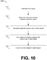
- Figure 10 shows an example method 1000 for conditioning an output signal of a pair of inductive sensor elements.
- a drive signal is generated. In some examples this may be carried out by a signal generator, such as signal generator 110 of Figure 1 .
- the drive signal may be sinusoidal drive signal 112 of Figure 1 .
- the drive signal is used to drive a pair of inductive sensor elements.
- the pair of inductive sensor elements may be connected in a half bridge arrangement.
- the pair of inductive sensor elements may be the same as inductive sensor element arrangement 132a, 132b or inductive sensor element arrangement 134a, 143b of Figure 1 .
- an adjustably scaled copy of the drive signal is generated.
- the adjustably scaled copy of the drive signal is isolated from the drive signal via isolation means.
- the isolation means may be one or more isolating transformers.
- the scaled copy of the drive signal is adjusted via one or more of a potentiometer, a digitally controlled potentiometer, or selected fixed resistors.
- an output signal of the pair of inductive sensor elements is summed with the adjustably scaled copy of the drive signal.
- the summed signal is converted to a digital signal.
- the summed signal is converted using one or more Analogue-to-Digital Converters, such as Analogue-to-Digital Converter 250 of Figure 2 or Figure 5 .
- a benefit of the improved signal conditioning circuit disclosed herein is that the improved signal conditioning circuit permits looser tolerances on the concentricity between the touchdown bearings, whilst still maintaining an optimal signal to noise ratio.
- the improved signal conditioning circuit is also tolerant of mismatches in the impedance of the opposed inductive sensor elements forming each half bridge arrangement.
- the improved signal conditioning circuit disclosed herein is applicable to both radial and axial sensor arrangements used in Active Magnetic Bearing systems.
- the use of the improved signal conditioning circuit can reduce the need for mechanical shims normally used to align the electrical centre of the half bridge inductive sensor arrangement in the axial direction with the mechanical centre of the touchdown bearings in the axial direction.
- the teachings herein are presented with reference to inductive position sensing elements. It should be understood that the teachings are equally applicable to eddy-current position sensing elements which is not covered by the scope of the claims.
- the reference ring may be constructed of a solid conducting material.
- the frequency of the sinusoidal drive signal may be higher than for implementations using inductive position sensing elements.
Landscapes
- Physics & Mathematics (AREA)
- General Physics & Mathematics (AREA)
- Engineering & Computer Science (AREA)
- General Engineering & Computer Science (AREA)
- Mechanical Engineering (AREA)
- Electromagnetism (AREA)
- Magnetic Bearings And Hydrostatic Bearings (AREA)
- Transmission And Conversion Of Sensor Element Output (AREA)
- Measurement Of Length, Angles, Or The Like Using Electric Or Magnetic Means (AREA)
Description
- The present invention relates to the field of electronics in general. In particular, the invention relates to an improved signal conditioning circuit for use with active magnetic bearings.
- Active magnetic bearings for supporting a rotor traditionally comprise electromagnets with variable excitation controlled by displacement sensors using electronic servo circuits. The displacement sensors are sensitive to changes in the position of the rotor relative to a reference position. The displacement sensors may be of the optical, capacitive, eddy current or inductive type.
- An inductive position sensor comprises a set of inductive elements with a variable gap fixed to the stator and cooperating with a reference ring, or 'target', integral with the rotor. The reference ring traditionally comprises a ring composed of magnetic sheets or made of ferrite. The reference ring must be manufactured with great care, as manufacturing defects and build tolerances limit the performance of the inductive sensor elements.
- Bridge type inductive position sensors used for magnetic bearing applications traditionally use a phase sensitive (synchronous) de-modulation circuit implemented using analogue electronics. In order to optimise the performance of the synchronous de-modulation circuit, the phase of the reference waveform should be adjusted to match the phase of the output signal from the sensor when the rotor is displaced from the centre position. With analogue synchronous de-modulation circuits, this phase shifting is traditionally performed using RC filter networks which are matched when the system is in its final installation with the field cabling installed.
- With the move towards automated and remote commissioning of magnetic bearing systems, this type of adjustment within the controller circuitry is inconvenient and a method of optimising the phase of the demodulation circuit remotely or automatically is desirable.
- Accordingly, an improved signal conditioning circuit for use with magnetic bearings is desirable.
- Document
US 3,650,581 discloses a mechanical contact-free bearing system for a rotor comprising a magnetic system which includes at least one carrier magnet for suspending the rotor with its axis vertical. -
Document GB 1 500 809 -
- Document
US 2014/252899 discloses a rotating electrical machine including a stator, a rotor, and at least one active magnetic bearing including a bearing winding, which is an air-gap winding, and includes at least a first phase winding and a second phase winding. - Embodiments of the invention are set out in the appended claims.
- The present invention provides an inductive sensing circuit comprising: a signal generator, configured to generate a drive signal; one or more sensing arrangements, each of the one or more sensing arrangements comprising: two sets of one or more inductive sensing elements configured in a half bridge arrangement, the two sets of one or more inductive sensing elements driven by the drive signal; a correction signal circuit configured to generate a correction signal, wherein the correction signal is an adjustably scaled version of the drive signal; and a summing circuit configured to sum an output signal of the two sets of one or more inductive sensing elements with the correction signal; and a demodulation circuit, configured to demodulate an output of the summing circuit of each of the one or more sensing arrangements.
- The present invention also provides a method for correcting an output signal of two sets of one or more inductive sensor elements, the method comprising: generating a drive signal; driving the two sets of one or more inductive sensor elements by applying the drive signal; generating a correction signal, wherein the correction signal is an adjustably scaled copy of the drive signal; summing the output signal of the two sets of one or more inductive sensor elements with the correction signal; and demodulating the summed signal.
- The present invention also provides an active magnetic bearing comprising the inductive sensing circuit disclosed herein.
- Further details, aspects and embodiments of the invention will be described, by way of example only, with reference to the drawings. In the drawings, like reference numbers are used to identify like or functionally similar elements. Elements in the figures are illustrated for simplicity and clarity and have not necessarily been drawn to scale.
-
Figure 1 shows a high level block diagram of a typical radial inductive position sensor arrangement. -
Figure 2 shows the block diagram of a typical digital implementation for an inductive position sensor element arrangement. -
Figure 3 shows an example of the output signal of a half bridge formed by an opposed pair of inductive sensor elements as the rotor is traversed in one axis of motion from contacting touchdown bearings on one side, through the mechanical centre position, to contacting the touchdown bearings on the opposite side, for an ideal system. -
Figure 4 shows an example of an offset waveform resulting from build tolerances causing the electrical or mechanical centre of the sensor elements to be offset from the mechanical centre of the touchdown bearings. -
Figure 5 shows a typical geometry for a radial inductive position sensor used within an Active Magnetic Bearing system. -
Figure 6 shows a typical geometry for an axial inductive position sensor used within an Active Magnetic Bearing system. -
Figure 7 shows a typical geometry using a disk as a reference ring for an axial inductive position sensor used within an Active Magnetic Bearing system. -
Figure 8 shows an improved sensor design for an inductive position sensor arrangement, in accordance with embodiments of the disclosure. -
Figure 9 shows an example corrected waveform derived from a raw sensor signal such as inFigure 4 obtained using the improved sensor design, along with an in-phase component of the corrected waveform. -
Figure 10 shows a flowchart of a method for conditioning output signals from an inductive sensor arrangement. - Embodiments of the invention disclosed herein provide inductive position sensing apparatus and methods which are tolerant to errors from manufacturing tolerances of the reference ring or inductive sensor elements, but are also tolerant to mismatches in the impedance of opposed inductive sensing elements.
- Throughout the following disclosure, reference shall be made to "inductive sensor elements". It should be understood that each inductive sensor element may not be a singular inductive sensor element, but instead may be one or more inductive sensor elements in a series arrangement.
-
Figure 1 shows a high level block diagram of a typical radial inductive position sensor arrangement. Typically, synchronous de-modulation of the "in-phase" component of the signal is used to remove noise and/or interfering signals from the sensor outputs.Figure 1 shows a plurality ofinductive sensor elements rotor 102.Inductive sensor elements Inductive sensor elements inductive sensor elements rotor 102. Likewise, the second pair ofinductive elements rotor 102. Asignal generator 110 is configured to generate asinusoidal drive signal 112. In some embodiments the drive signal may be non-sinusoidal and could be, for example, a square wave.Signal generator 110 is operably coupled to abalanced voltage drive 120.Signal generator 110 also provides a synchronisation signal to first and secondsynchronous de-modulation circuitry synchronous de-modulation circuitry - First pair of
inductive sensor elements inductive sensor elements first output 122 ofbalanced voltage drive 120 is coupled to a first input of each of the first and second half bridge arrangements. Asecond output 124 ofbalanced voltage drive 120 is coupled to a second input of each of the first and second half bridge arrangements. Optionally,balanced voltage drive 120 may include circuitry configured to amplify thesinusoidal drive signal 122 from thesignal generator 110. Although examples and embodiments herein reference use ofbalanced voltage drive 120, it should be understood that in some alternative embodiments a single-ended voltage drive may be used instead. Anoutput 142 from the first half bridge arrangement is operably coupled to a first input of first optionalsignal conditioning circuitry 180. A first output 142' of first optionalsignal conditioning circuitry 180 is coupled to a first input of secondsynchronous de-modulation circuitry 154. Anoutput 144 from the second half bridge arrangement is operably coupled to a second input of first optionalsignal conditioning circuitry 180. A second output 144' of first optionalsignal conditioning circuitry 180 is coupled to a second input of secondsynchronous de-modulation circuitry 154. Secondsynchronous de-modulation circuitry 154 is configured to remove noise and/or interfering signals from each of outputs 142' and 144' of the first (132a, 132b) and second (134a, 134b) half bridge inductive sensor element arrangements or optionalsignal conditioning circuitry 180 such that only the respective sensor output remains (i.e. the signal which indicates the position of therotor 102 along a particular axis). -
Element 158 converts a copy ofoutputs 122 and 124 (one or both) ofbalanced voltage drive 120 into a single endedsignal 159. Single ended signal 159 fromelement 158 is operably coupled to an input of second optionalsignal conditioning circuitry 181. An output 159' of second optionalsignal conditioning circuitry 181 is coupled to an input of firstsynchronous de-modulation circuitry 152. Firstsynchronous de-modulation circuitry 152 is configured to remove noise and/or interfering signals from single endedsignal 159. First andsecond outputs synchronous de-modulation circuitry 154 are operably coupled to first and second inputs ofratiometric block 156.Output 166 of firstsynchronous de-modulation circuitry 152 is operably coupled to a third input ofratiometric block 156. Although first and secondsynchronous de-modulation circuitry Figure 1 , they may be implemented as a single circuit or as two or more separate circuits. Similarly, first and second optionalsignal conditioning circuitry Ratiometric block 156 is configured to convertsensor signals Signal 166 is used as a reference signal in convertingsignals balanced voltage drive 120. Synchronous de-modulation can be performed using either analogue implementations or digital implementations. - In some examples,
inductive sensor elements inductive sensor elements inductive sensor elements inductive sensor elements inductive sensor elements -
Figure 2 shows a typical sensor design for use with digital implementations of synchronous de-modulation of the inductive position sensor element output signals. The circuit ofFigure 2 provides an implementation of the elements ofFigure 1 insidebox 170.Figure 2 shows asignal generator 110, which is used to generate asinusoidal drive signal 112 at a required frequency. In the embodiment ofFigure 2 ,signal generator 110 generates the signal digitally, however alternative embodiments may instead use an analogue signal generating stage. Thesignal generator 110 is operably coupled to a Digital-to-Analogue Converter (DAC) 212. The output of Digital-to-Analogue Converter (DAC) 212 is operably coupled to an Alternating Current (AC)couple 214.AC couple 214 is configured to eliminate any Direct Current (DC) component of thesinusoidal drive signal 112. TheAC couple 214 may be, for example, a suitably sized capacitor. The output ofAC couple 214 is operably coupled to apower amplifier 216.Power amplifier 216 is coupled tobalanced voltage drive 120. In the embodiment ofFigure 2 , thebalanced voltage drive 120 is implemented using a transformer with multiple secondary windings, however in other embodiments alternative means of implementing a balanced voltage drive may be used. A reference signal frombalanced voltage drive 120 is coupled toamplifier 240, in order to provide a reference signal for performing the ratiometric function ofratiometric block 156. Afirst output 122 ofbalanced voltage drive 120 is coupled to a first input of each of the first (132a, 132b) and second (134a, 134b) half bridge inductive sensor element arrangements. Asecond output 124 ofbalanced voltage drive 120 is coupled to a second input of each of the first (132a, 132b) and second (134a, 134b) half bridge inductive sensor element arrangements. The sensedsignal 142 from first pair ofinductive sensor elements amplifier 242. The sensed signal from second pair ofinductive sensor elements amplifier 244. In some embodiments, amplifier stages 240, 242 and 244 may have adjustable gain. Therespective outputs analogue signals Digital Converter 250 is coupled to an input of firstsynchronous de-modulation circuitry 152 ofFigure 1 . Outputs 142' and 144' of Analogue-to-Digital Converter 250 are coupled to first and second outputs of secondsynchronous de-modulation circuitry 154 ofFigure 1 . Amplifier stages 240, 242 and 244 and Analogue-to-Digital Converter 250 may correspond to signalconditioning elements Figure 1 . First and secondsynchronous de-modulation circuitry ratiometric block 156 in the same manner as inFigure 1 . In the embodiment ofFigure 2 ,synchronous demodulation circuitry ratiometric block 156, are implemented digitally. - Some digital implementations of the
synchronous de-modulation circuitry ratiometric block 156 may combine Field Programmable Gate Arrays (FPGAs) or other control logic to handle the phase shifting and multiplication functions used for performing synchronous demodulation, and Digital Signal Processors (DSPs) or other control processing to handle the ratiometric function. The DSPs may also be used to perform Active Magnetic Bearing servo control functions. In some embodiments, digital synchronous de-modulation of the output signal may comprise aprogramable signal generator 110 used to construct asinusoidal drive signal 112 at a required frequency. In addition to thesinusoidal drive signal 112, thesignal generator 110 may be configured to output a synchronising pulse for use by the first and secondsynchronous de-modulation circuitry ratiometric block 156. Thesignal generator 110 may be under the control of a supervisory FPGA or other control logic which may also be responsible for data communications and/or a supervisory state machine or other control logic which controls the sequencing of an overall Active Magnetic Bearing control system, which may include actuator elements or electromagnetic elements. Each Active Magnetic Bearing for use in a given installation may have its own control logic and/or processing, or control logic and/or processing may be shared between multiple Active Magnetic Bearings in a given installation. - Motion of a
rotor 102 supported by an Active Magnetic Bearing system according to the present disclosure may be typically constrained by mechanical "touchdown bearings" (one at each end of the rotor 102). These will normally be operational with a clearance, but when the rotor moves out of position the rotor may contact the touchdown bearings. The Active Magnetic Bearing system will normally be configured with the "centre" position defined by the mechanical centre of the touchdown bearing clearances, as opposed to the mechanical centre of the sensor clearances or the mechanical centre of the actuator clearances. -
Figure 3 shows a sinusoidal drive signal waveform 310 (which may be, for example,sinusoidal drive signal 112 generated bysignal generator 110 ofFigure 1 orFigure 2 ), and the ideal output signal of a half bridge inductive sensor element arrangement (which may be, for example, either half bridge inductivesensor element arrangement sensor element arrangement rotor 102 traverses (in one axis of motion) from contacting the touchdown bearings on one side (waveform 320), through the mechanical centre position (waveform 324) to contacting the touchdown bearings on the opposite side (waveform 322), for an ideal system. - The input gain on the Analogue-to-
Digital Converter 250 may be set to optimise the usage of the available Analogue-to-Digital Converter 250 input range for the allowable range of motion (between contacting the touchdown bearings on one side and contacting the touchdown bearings on the other side). This is done in order to maximise signal to noise ratio and minimise the effects of quantisation noise (i.e. noise caused by the error between the real analogue value of the signal input to theADC 250 and the sampled output value associated with the input signal). Similar input range considerations apply for analogue implementations of the synchronous de-modulation circuit and ratiometric block. - However, due to build tolerances the mechanical centre of the half bridge inductive sensor element arrangement may be offset from the mechanical centre of the touchdown bearings (i.e. a misalignment between mechanical centre of the half bridge inductive sensor element arrangement and the mechanical centre of the touchdown bearings). In this case, the output signal of the sensor as the
rotor 102 traverses (in one axis of motion) from contacting the touchdown bearings on one side (waveform 420), through the mechanical centre position of the touchdown bearings (waveform 424) to contacting the touchdown bearings on the opposite side (waveform 422) could be, for example, as shown inFigure 4 . - Additionally, due to constructional and material tolerance of the inductive sensor elements, the inductive sensor elements may not be perfectly matched, resulting in the null (minimum) output from the half bridge inductive sensor element arrangement being offset from the mechanical centre of the half bridge arrangement. This null is referred to as the electrical centre of the half bridge inductive sensor element arrangement.
- In the particular case of
Figure 4 , the input gain for the Analogue-to-Digital Converter 250 may be set so that the largest signal (for example, withamplitude 3A inFigure 4 , where A is an arbitrary value representing the amplitude of the signal) observed when traversing therotor 102 can be correctly sampled by the Analogue-to-Digital Converter 250 (or the front end of the analogue circuit where the synchronous de-modulation is implemented using analogue components). In the particular case shown inFigure 4 , the effect of this would be to reduce the sensitivity at the input of thesynchronous demodulation circuit 152, 154 (or Analogue-to-Digital Converter 250) by a factor of 1/3, with a corresponding decrease in signal to noise ratio. -
Figure 5 shows an example of a typical construction of a radial inductive sensor arrangement used within an Active Magnetic Bearing system, as perFigure 1 .Figure 5 showsrotor shaft 502, withlaminated reference ring 510. Inductive sensor element R1+ has laminatedcore 520 and coils 522 and 524. Inductive sensor element R2+ has laminatedcore 530 and coils 532 and 534. Inductive sensor element R1- has laminatedcore 540 and coils 542 and 544. Inductive sensor element R2- has laminatedcore 550 and coils 552 and 554. Inductive sensor element R1+ is arranged diametrically opposite inductive sensor element R1-. Inductive sensor element R2+ is arranged diametrically opposite inductive sensor element R2-. Inductive sensor elements R1+ and R1- are electrically connected in a first half bridge arrangement. Inductive sensor elements R2+ and R2- are electrically connected in a second half bridge arrangement.Figure 5 does not show any of the actuator parts or the touchdown bearings of an Active Magnetic Bearing system, and merely serves to illustrate one example arrangement of sensor elements. -
Figure 6 shows an example of a typical construction of an axial inductive slip sensor arrangement used within an Active Magnetic Bearing system, which may be used to detect the position of the rotor along the rotor axis. As with a radial sensor arrangement ofFigure 5 , in the axial arrangement the inductive sensor is formed of pairs of opposed inductive sensor elements each wired to form a half bridge arrangement, and arranged along the axis of the rotor.Figure 6 shows a core shaft orrotor 602 withlaminated reference ring 610.Laminated reference ring 610 may be supported by non-activemechanical support parts mechanical support parts laminated reference ring 610 compressed. Non-activemechanical support parts laminated reference ring 610 and non-activemechanical support parts Inductive sensing elements 620 and 640 (which may alternatively be referred to as axial sensor rings) together form one element of a half bridge arrangement. Sensingelements Figure 6 does not show any of the actuator parts or the touchdown bearings of an Active Magnetic Bearing system, and merely serves to illustrate one example arrangement of sensor elements. -
Figure 7 shows an alternative example of a typical construction of an axial inductive sensor arrangement using a disk as the target.Figure 7 shows arotor 702 with a solid ferrite disc orlaminated reference ring 710.Inductive sensing elements Inductive sensing elements Figure 7 does not show any of the actuator parts or the touchdown bearings of an Active Magnetic Bearing system, and merely serves to illustrate one example arrangement of sensor elements. - An improved signal conditioning circuit disclosed herein provides the addition of a controlled amount of the sinusoidal drive signal used within the drive circuit to the signals output by the half bridge inductive sensor element arrangements (132a, 132b; 134a, 134b). The added signal will be of a controlled amplitude and for a particular axis, and may be of either positive or negative phase depending on the required correction for the particular half bridge sensor element arrangement.
-
Figure 8 shows a schematic of an improved sensor and signal conditioning circuit design in accordance with embodiments of the disclosure. The improved signal conditioning circuit ofFigure 8 is an improved version of the signal conditioning circuit ofFigure 2 . Accordingly, the same reference numerals are used to indicate elements which are the same as those inFigure 2 .Figure 8 showssignal generator 110 used to generate a sinusoidal drive signal at a required frequency.Signal generator 110 is coupled byconnection 811 to supply a copy ofdrive signal 112 to a negative gain circuitry 820 (which may be alternatively referred to as an inverting amplifier, which may or may not have unity gain), and to a first input of each of first and second correction signal adjustment means 832 and 834 (where correction signal adjustment means 832 and 834 may be, for example, a potentiometer).Negative gain circuitry 820 is configured to generate a copy ofdrive signal 112 with an inverted polarity. An output ofnegative gain circuitry 820 is coupled byconnection 821 to a second input of each of first and second correctionsignal adjustment potentiometers signal adjustment potentiometers correction signal output 833 of first correctionsignal adjustment potentiometer 832 is summed with the sensedsignal 142 from first pair ofinductive sensor elements block 842. Likewise, the secondcorrection signal output 835 of second correctionsignal adjustment potentiometer 834 is summed with the sensedsignal 144 from the second pair ofinductive sensor elements block 844. Theoutputs blocks amplifier stages Figure 2 , theoutputs block 801 may collectively be referred to assignal correction circuitry 801. - Optionally, first and second correction signals 833 and 835 may be isolated from
signal generator 110 by use of atransformer 810 or other such isolating means in order to reduce the effect of ground noise on first and second correction signals 833 and 835. In some embodiments, a separate isolation means may be used for each of correction signals 833 and 835. - In
Figure 8 , the scaling of first and second correction signals 833 and 835 is shown as being controlled by first and second correctionsignal adjustment potentiometers - The embodiment of
Figure 8 provides an inductive sensor element arrangement and signal conditioning circuit for two-axis sensing of an Active Magnetic Bearing. Alternative embodiments may provide sensor element arrangements and signal conditioning circuits for one or more axes of detection. - The effect of applying the correction signals (for the ideal circuit) is to bring the resulting signal amplitude to zero when the rotor is at the mechanical centre of the touchdown bearings, and to achieve a similar amplitude at the two extreme positions (but with opposed phase for the two extreme positions), as for the ideal waveforms shown in
Figure 3 . - In some embodiments the input gains 242 and 244 to Analogue-to-
Digital Converter 250 may be adjustable to facilitate further optimisation of the signal amplitude with respect to the input range of the Analogue-to-Digital Converter 250 (or analogue synchronous de-modulation circuitry for an analogue implementation), as noted above with respect toFigure 2 . - In practice, due to mismatched inductances, capacitive cable effects and resistance, the corrected output signal at the mechanical centre position may be a non-zero quadrature signal, but when synchronously de-modulated this gives zero in-phase signal as desired.
Figure 9B shows an example of a corrected output signal where the signal at the mechanical centre position (waveform 924) is a non-zero quadrature signal, wherewaveform 920 shows the signal for maximum positive displacement ofrotor 102 andwaveform 922 shows the signal for maximum negative displacement ofrotor 102. The non-perfect quadrature signal when at the mechanical centre position does not affect the improvement in signal to noise ratio achieved by the improved signal conditioning circuit disclosed herein.Figure 9C shows the in-phase components (930, 932, 934) of the corrected waveform, wherewaveform 930 shows the signal for maximum positive displacement ofrotor 102,waveform 932 shows the signal for maximum negative displacement ofrotor 102, and waveform 934 shows the signal forrotor 102 in the mechanical centre position. -
Figure 10 shows anexample method 1000 for conditioning an output signal of a pair of inductive sensor elements. Atblock 1010, a drive signal is generated. In some examples this may be carried out by a signal generator, such assignal generator 110 ofFigure 1 . In some examples the drive signal may besinusoidal drive signal 112 ofFigure 1 . Atblock 1020, the drive signal is used to drive a pair of inductive sensor elements. In some examples, the pair of inductive sensor elements may be connected in a half bridge arrangement. The pair of inductive sensor elements may be the same as inductivesensor element arrangement sensor element arrangement 134a, 143b ofFigure 1 . Atblock 1030 an adjustably scaled copy of the drive signal is generated. In some examples, the adjustably scaled copy of the drive signal is isolated from the drive signal via isolation means. In some examples the isolation means may be one or more isolating transformers. In some examples the scaled copy of the drive signal is adjusted via one or more of a potentiometer, a digitally controlled potentiometer, or selected fixed resistors. Atblock 1040, an output signal of the pair of inductive sensor elements is summed with the adjustably scaled copy of the drive signal. Atblock 1050 the summed signal is converted to a digital signal. In some examples, the summed signal is converted using one or more Analogue-to-Digital Converters, such as Analogue-to-Digital Converter 250 ofFigure 2 orFigure 5 . - A benefit of the improved signal conditioning circuit disclosed herein is that the improved signal conditioning circuit permits looser tolerances on the concentricity between the touchdown bearings, whilst still maintaining an optimal signal to noise ratio. The improved signal conditioning circuit is also tolerant of mismatches in the impedance of the opposed inductive sensor elements forming each half bridge arrangement.
- The improved signal conditioning circuit disclosed herein is applicable to both radial and axial sensor arrangements used in Active Magnetic Bearing systems.
- For axial bearings, the use of the improved signal conditioning circuit can reduce the need for mechanical shims normally used to align the electrical centre of the half bridge inductive sensor arrangement in the axial direction with the mechanical centre of the touchdown bearings in the axial direction.
- For a typical Active Magnetic Bearing there will typically be one signal conditioning circuit for each axis of the Active Magnetic Bearing system.
- The teachings herein are presented with reference to inductive position sensing elements. It should be understood that the teachings are equally applicable to eddy-current position sensing elements which is not covered by the scope of the claims. In some examples implementing eddy-current sensor elements, the reference ring may be constructed of a solid conducting material. In some examples using eddy-current sensor elements, the frequency of the sinusoidal drive signal may be higher than for implementations using inductive position sensing elements.
- While several embodiments have been provided in the present disclosure, it should be understood that the disclosed systems and methods may be embodied in many other specific forms without departing from the scope of the present disclosure as defined by the appended claims. The present examples are to be considered as illustrative and not restrictive, and the intention is not to be limited to the details given herein. For example, various elements or components may be combined or integrated in another system or certain features may be omitted, or not implemented.
Claims (15)
- An inductive sensing circuit, comprising:a signal generator (110), configured to generate a drive signal (112);one or more sensing arrangements, each of the one or more sensing arrangements comprising:two sets of one or more inductive sensing elements (132a, 132b; 134a, 134b), configured in a half bridge arrangement, the two sets of one or more inductive sensing elements driven by the drive signal (112);a correction signal circuit (801), configured to generate a correction signal (833, 835), wherein the correction signal is an adjustably scaled version of the drive signal; anda summing circuit (842, 844), configured to sum an output signal (142, 244) of the two sets of one or more inductive sensing elements with the correction signal; anda demodulation circuit, configured to demodulate an output of the summing circuit (842, 844) of each of the one or more sensing arrangements.
- The inductive sensing circuit of claim 1, wherein the demodulation circuit comprises an analogue to digital converter (250) configured to convert an output of the summing circuit of each of the one or more sensing arrangements to a corresponding digital output signal (142', 144').
- The inductive sensing circuit of claim 1 or 2, wherein each of the one or more sensing arrangements further comprises a signal adjustment means (832, 834) configured to adjust the scaling of the correction signal.
- The inductive sensing circuit of any of claims 1 to 3, wherein each of the one or more sensing arrangements further comprises an amplifier circuit (242, 244) coupled between an output of the summing circuit and the demodulation circuit; and/or
further comprising a transformer (810) to isolate the signal generator from the correction signal circuit of each of the one or more sensing arrangements. - The inductive sensing circuit of any of claims 1 to 4, wherein the drive signal is a sinusoidal signal; and/orfurther comprising means (214) for removing a DC component of the drive signal; and/orfurther comprising a balanced voltage drive (120), configured to drive the two sets of one or more inductive sensing elements of each of the one or more sensing arrangements.
- The inductive sensing circuit of any of claims 2 to 5, wherein the demodulation further comprises one or more synchronous de-modulation circuits coupled to one or more outputs of the analogue-to-digital converter (250); and optionally
wherein the one or more synchronous de-modulation circuits are configured to remove noise from the one or more outputs of the analogue-to-digital converter. - The inductive sensing circuit of any of claims 1 to 6, further comprising means for performing a ratiometric function; and/orwherein the signal generator (110) is configured to provide a synchronisation signal to one or more of the synchronous de-modulation circuits; and/orwherein the inductive sensor elements are eddy current sensor elements.
- An active magnetic bearing, comprising the inductive sensing circuit of any preceding claim.
- The active magnetic bearing of claim 8, further comprising a rotor; andwherein the two sets of inductive sensing elements of a first sensing arrangement of the one or more sensing arrangements are arranged about a circumference of the rotor; and/orwherein the two sets of inductive sensing elements of a first sensing arrangement of the one or more sensing arrangements are arranged along an axis of the rotor.
- A method for correcting an output signal of two sets of one or more inductive sensor elements, the method comprising:generating a drive signal (112);driving the two sets of one or more inductive sensor elements (132a, 132b; 134a, 134b) by applying the drive signal;generating a correction signal (833, 835), wherein the correction signal is an adjustably scaled copy of the drive signal;summing the output signal (42, 144) of the two sets of one or more inductive sensor elements with the correction signal; anddemodulating the summed signal (243, 245).
- The method of claim 10, wherein demodulating the summed signal comprises converting the summed output signal (243, 245) of the two sets of one or more inductive sensor elements to a corresponding digital output signal (142', 144').
- The method of claim 10 or 11, further comprising adjusting the scaling of the correction signal via a signal adjustment means (832, 834); and/or
amplifying the summed output signal of the two sets of one or more inductive sensor elements. - The method of any of claims 10 to 12, further comprising isolating a copy of the drive signal for use in generating the correction signal; and/or
further comprising removing a DC component of the drive signal. - The method of any of claims 10 to 13, wherein demodulating the summed signal further comprises synchronously demodulating the digital output signal; and optionally
wherein synchronously demodulating the digital output signal comprises removing noise from the digital output signal. - The method of claim 14, further comprising performing a ratiometric function.
Applications Claiming Priority (1)
| Application Number | Priority Date | Filing Date | Title |
|---|---|---|---|
| GB1903224.2A GB2582286B (en) | 2019-03-08 | 2019-03-08 | Improved signal conditioning circuit for use with active magnetic bearings |
Publications (2)
| Publication Number | Publication Date |
|---|---|
| EP3705839A1 EP3705839A1 (en) | 2020-09-09 |
| EP3705839B1 true EP3705839B1 (en) | 2022-12-28 |
Family
ID=66380524
Family Applications (1)
| Application Number | Title | Priority Date | Filing Date |
|---|---|---|---|
| EP20161656.2A Active EP3705839B1 (en) | 2019-03-08 | 2020-03-06 | Improved signal conditioning circuit for use with active magnetic bearings |
Country Status (5)
| Country | Link |
|---|---|
| US (1) | US11428547B2 (en) |
| EP (1) | EP3705839B1 (en) |
| JP (1) | JP7514087B2 (en) |
| CN (1) | CN111664779B (en) |
| GB (1) | GB2582286B (en) |
Families Citing this family (4)
| Publication number | Priority date | Publication date | Assignee | Title |
|---|---|---|---|---|
| US10975908B1 (en) * | 2019-10-29 | 2021-04-13 | Schaeffler Monitoring Services Gmbh | Method and device for monitoring a bearing clearance of roller bearings |
| CN113833757B (en) * | 2021-09-23 | 2022-08-02 | 北京航空航天大学 | Five-degree-of-freedom rotor axial displacement self-sensing magnetic suspension bearing |
| CN115507742B (en) * | 2022-09-30 | 2026-03-06 | 九江精密测试技术研究所 | A circuit for testing the installation of a turntable motor |
| CN115615304B (en) * | 2022-12-20 | 2023-06-02 | 苏州苏磁智能科技有限公司 | Magnetic suspension motor, position detection sensor and sensor detection circuit |
Family Cites Families (12)
| Publication number | Priority date | Publication date | Assignee | Title |
|---|---|---|---|---|
| DE1933031C3 (en) | 1969-06-30 | 1978-10-26 | Karl 5170 Juelich Boden | Magnetic storage |
| DE2457084A1 (en) | 1974-02-09 | 1976-06-10 | Licentia Gmbh | RADIAL ACTIVE MAGNETIC BEARING |
| US4967154A (en) * | 1989-09-13 | 1990-10-30 | Optima Industries, Inc. | Dynamic tube runout measuring method and apparatus with square wave energized reluctance measuring coils |
| JP3649057B2 (en) | 1999-09-27 | 2005-05-18 | 日本精工株式会社 | Torque sensor |
| GB0126014D0 (en) * | 2001-10-30 | 2001-12-19 | Sensopad Technologies Ltd | Modulated field position sensor |
| US8258777B2 (en) * | 2009-09-04 | 2012-09-04 | Weihua Chen | Inductive proximity sensor |
| EP2402777B1 (en) * | 2010-06-30 | 2013-01-09 | LEM Intellectual Property SA | Autonomously calibrated magnetic field sensor |
| EP2589827A1 (en) | 2011-11-04 | 2013-05-08 | ETH Zürich | Rotating electrical machine and method for measuring a displacement of a rotating electrical machine |
| EP2781887B1 (en) | 2013-03-19 | 2016-08-10 | Skf Magnetic Mechatronics | Variable inductance type position sensor system and method |
| DE102014010671A1 (en) * | 2014-05-23 | 2015-12-17 | Gerd Reime | Method for determining at least one physical parameter by means of a sensor unit |
| CN105823452B (en) * | 2016-04-29 | 2017-11-14 | 北京航空航天大学 | A kind of magnetic bearing displacement transducer displacement signal Opsonizing method |
| JP6677663B2 (en) * | 2017-02-17 | 2020-04-08 | 株式会社東芝 | Motor control device and motor drive device |
-
2019
- 2019-03-08 GB GB1903224.2A patent/GB2582286B/en not_active Expired - Fee Related
-
2020
- 2020-03-04 US US16/808,744 patent/US11428547B2/en active Active
- 2020-03-05 JP JP2020037549A patent/JP7514087B2/en active Active
- 2020-03-06 EP EP20161656.2A patent/EP3705839B1/en active Active
- 2020-03-09 CN CN202010157273.2A patent/CN111664779B/en active Active
Also Published As
| Publication number | Publication date |
|---|---|
| GB201903224D0 (en) | 2019-04-24 |
| GB2582286B (en) | 2021-05-12 |
| GB2582286A (en) | 2020-09-23 |
| US20200284617A1 (en) | 2020-09-10 |
| EP3705839A1 (en) | 2020-09-09 |
| CN111664779B (en) | 2024-09-17 |
| JP2020169978A (en) | 2020-10-15 |
| CN111664779A (en) | 2020-09-15 |
| JP7514087B2 (en) | 2024-07-10 |
| US11428547B2 (en) | 2022-08-30 |
Similar Documents
| Publication | Publication Date | Title |
|---|---|---|
| US11428547B2 (en) | Signal conditioning circuit for use with active magnetic bearings | |
| CN102472640B (en) | Resolver signal conversion device and method | |
| US4843292A (en) | Direct drive motor system | |
| JP6171375B2 (en) | Magnetic bearing device and vacuum pump | |
| CN105823452B (en) | A kind of magnetic bearing displacement transducer displacement signal Opsonizing method | |
| WO2017024119A1 (en) | Homopolar, flux-biased hysteresis bearingless motor | |
| Zare et al. | The effect of winding arrangements on measurement accuracy of sinusoidal rotor resolver under fault conditions | |
| CN107063075B (en) | Angle detection equipment | |
| EP3517896B1 (en) | Contactless radial position sensor having improved response behavior to target defects | |
| US10436609B2 (en) | Position sensor assembly | |
| WO2014195424A1 (en) | Rotary encoder | |
| US6442210B1 (en) | Apparatus for AC-to-DC conversion which provides a signed DC signal | |
| CN106655685A (en) | Rotary transformer and rotating body equipped with same | |
| US4568865A (en) | Self-corrected synchro/resolver | |
| CN117411371A (en) | High-precision servo control system | |
| KR20130059230A (en) | Device for compensating of the thermal errors for machine tool | |
| JP6320098B2 (en) | Variable inductance type position sensor system and variable inductance type method | |
| WO2018037158A1 (en) | A stator module for an axial magnetic bearing | |
| JP2010164450A (en) | Resolver digital converter | |
| Verma et al. | Design considerations for resolver-to-digital converters in electric vehicles | |
| Aung | Analysis and synthesis of precision resolver system | |
| CN114252766A (en) | Sensor and method for extracting rotation angle and rotation speed signals | |
| CN119572622A (en) | Analog compensation of inductive sensors | |
| Alipour-Sarabi et al. | Linearized resolver | |
| JP2023018461A (en) | Adjustment method of differential resolver and differential resolver |
Legal Events
| Date | Code | Title | Description |
|---|---|---|---|
| PUAI | Public reference made under article 153(3) epc to a published international application that has entered the european phase |
Free format text: ORIGINAL CODE: 0009012 |
|
| STAA | Information on the status of an ep patent application or granted ep patent |
Free format text: STATUS: THE APPLICATION HAS BEEN PUBLISHED |
|
| AK | Designated contracting states |
Kind code of ref document: A1 Designated state(s): AL AT BE BG CH CY CZ DE DK EE ES FI FR GB GR HR HU IE IS IT LI LT LU LV MC MK MT NL NO PL PT RO RS SE SI SK SM TR |
|
| AX | Request for extension of the european patent |
Extension state: BA ME |
|
| STAA | Information on the status of an ep patent application or granted ep patent |
Free format text: STATUS: REQUEST FOR EXAMINATION WAS MADE |
|
| 17P | Request for examination filed |
Effective date: 20210309 |
|
| RBV | Designated contracting states (corrected) |
Designated state(s): AL AT BE BG CH CY CZ DE DK EE ES FI FR GB GR HR HU IE IS IT LI LT LU LV MC MK MT NL NO PL PT RO RS SE SI SK SM TR |
|
| GRAP | Despatch of communication of intention to grant a patent |
Free format text: ORIGINAL CODE: EPIDOSNIGR1 |
|
| STAA | Information on the status of an ep patent application or granted ep patent |
Free format text: STATUS: GRANT OF PATENT IS INTENDED |
|
| INTG | Intention to grant announced |
Effective date: 20220713 |
|
| GRAS | Grant fee paid |
Free format text: ORIGINAL CODE: EPIDOSNIGR3 |
|
| GRAA | (expected) grant |
Free format text: ORIGINAL CODE: 0009210 |
|
| STAA | Information on the status of an ep patent application or granted ep patent |
Free format text: STATUS: THE PATENT HAS BEEN GRANTED |
|
| AK | Designated contracting states |
Kind code of ref document: B1 Designated state(s): AL AT BE BG CH CY CZ DE DK EE ES FI FR GB GR HR HU IE IS IT LI LT LU LV MC MK MT NL NO PL PT RO RS SE SI SK SM TR |
|
| REG | Reference to a national code |
Ref country code: GB Ref legal event code: FG4D |
|
| REG | Reference to a national code |
Ref country code: CH Ref legal event code: EP |
|
| REG | Reference to a national code |
Ref country code: DE Ref legal event code: R096 Ref document number: 602020007137 Country of ref document: DE |
|
| REG | Reference to a national code |
Ref country code: AT Ref legal event code: REF Ref document number: 1540761 Country of ref document: AT Kind code of ref document: T Effective date: 20230115 |
|
| REG | Reference to a national code |
Ref country code: IE Ref legal event code: FG4D |
|
| REG | Reference to a national code |
Ref country code: LT Ref legal event code: MG9D |
|
| PG25 | Lapsed in a contracting state [announced via postgrant information from national office to epo] |
Ref country code: SE Free format text: LAPSE BECAUSE OF FAILURE TO SUBMIT A TRANSLATION OF THE DESCRIPTION OR TO PAY THE FEE WITHIN THE PRESCRIBED TIME-LIMIT Effective date: 20221228 Ref country code: NO Free format text: LAPSE BECAUSE OF FAILURE TO SUBMIT A TRANSLATION OF THE DESCRIPTION OR TO PAY THE FEE WITHIN THE PRESCRIBED TIME-LIMIT Effective date: 20230328 Ref country code: LT Free format text: LAPSE BECAUSE OF FAILURE TO SUBMIT A TRANSLATION OF THE DESCRIPTION OR TO PAY THE FEE WITHIN THE PRESCRIBED TIME-LIMIT Effective date: 20221228 Ref country code: FI Free format text: LAPSE BECAUSE OF FAILURE TO SUBMIT A TRANSLATION OF THE DESCRIPTION OR TO PAY THE FEE WITHIN THE PRESCRIBED TIME-LIMIT Effective date: 20221228 |
|
| REG | Reference to a national code |
Ref country code: NL Ref legal event code: MP Effective date: 20221228 |
|
| REG | Reference to a national code |
Ref country code: AT Ref legal event code: MK05 Ref document number: 1540761 Country of ref document: AT Kind code of ref document: T Effective date: 20221228 |
|
| PG25 | Lapsed in a contracting state [announced via postgrant information from national office to epo] |
Ref country code: RS Free format text: LAPSE BECAUSE OF FAILURE TO SUBMIT A TRANSLATION OF THE DESCRIPTION OR TO PAY THE FEE WITHIN THE PRESCRIBED TIME-LIMIT Effective date: 20221228 Ref country code: LV Free format text: LAPSE BECAUSE OF FAILURE TO SUBMIT A TRANSLATION OF THE DESCRIPTION OR TO PAY THE FEE WITHIN THE PRESCRIBED TIME-LIMIT Effective date: 20221228 Ref country code: HR Free format text: LAPSE BECAUSE OF FAILURE TO SUBMIT A TRANSLATION OF THE DESCRIPTION OR TO PAY THE FEE WITHIN THE PRESCRIBED TIME-LIMIT Effective date: 20221228 Ref country code: GR Free format text: LAPSE BECAUSE OF FAILURE TO SUBMIT A TRANSLATION OF THE DESCRIPTION OR TO PAY THE FEE WITHIN THE PRESCRIBED TIME-LIMIT Effective date: 20230329 |
|
| PG25 | Lapsed in a contracting state [announced via postgrant information from national office to epo] |
Ref country code: NL Free format text: LAPSE BECAUSE OF FAILURE TO SUBMIT A TRANSLATION OF THE DESCRIPTION OR TO PAY THE FEE WITHIN THE PRESCRIBED TIME-LIMIT Effective date: 20221228 |
|
| PG25 | Lapsed in a contracting state [announced via postgrant information from national office to epo] |
Ref country code: SM Free format text: LAPSE BECAUSE OF FAILURE TO SUBMIT A TRANSLATION OF THE DESCRIPTION OR TO PAY THE FEE WITHIN THE PRESCRIBED TIME-LIMIT Effective date: 20221228 Ref country code: RO Free format text: LAPSE BECAUSE OF FAILURE TO SUBMIT A TRANSLATION OF THE DESCRIPTION OR TO PAY THE FEE WITHIN THE PRESCRIBED TIME-LIMIT Effective date: 20221228 Ref country code: PT Free format text: LAPSE BECAUSE OF FAILURE TO SUBMIT A TRANSLATION OF THE DESCRIPTION OR TO PAY THE FEE WITHIN THE PRESCRIBED TIME-LIMIT Effective date: 20230428 Ref country code: ES Free format text: LAPSE BECAUSE OF FAILURE TO SUBMIT A TRANSLATION OF THE DESCRIPTION OR TO PAY THE FEE WITHIN THE PRESCRIBED TIME-LIMIT Effective date: 20221228 Ref country code: EE Free format text: LAPSE BECAUSE OF FAILURE TO SUBMIT A TRANSLATION OF THE DESCRIPTION OR TO PAY THE FEE WITHIN THE PRESCRIBED TIME-LIMIT Effective date: 20221228 Ref country code: CZ Free format text: LAPSE BECAUSE OF FAILURE TO SUBMIT A TRANSLATION OF THE DESCRIPTION OR TO PAY THE FEE WITHIN THE PRESCRIBED TIME-LIMIT Effective date: 20221228 Ref country code: AT Free format text: LAPSE BECAUSE OF FAILURE TO SUBMIT A TRANSLATION OF THE DESCRIPTION OR TO PAY THE FEE WITHIN THE PRESCRIBED TIME-LIMIT Effective date: 20221228 |
|
| PG25 | Lapsed in a contracting state [announced via postgrant information from national office to epo] |
Ref country code: SK Free format text: LAPSE BECAUSE OF FAILURE TO SUBMIT A TRANSLATION OF THE DESCRIPTION OR TO PAY THE FEE WITHIN THE PRESCRIBED TIME-LIMIT Effective date: 20221228 Ref country code: PL Free format text: LAPSE BECAUSE OF FAILURE TO SUBMIT A TRANSLATION OF THE DESCRIPTION OR TO PAY THE FEE WITHIN THE PRESCRIBED TIME-LIMIT Effective date: 20221228 Ref country code: IS Free format text: LAPSE BECAUSE OF FAILURE TO SUBMIT A TRANSLATION OF THE DESCRIPTION OR TO PAY THE FEE WITHIN THE PRESCRIBED TIME-LIMIT Effective date: 20230428 Ref country code: AL Free format text: LAPSE BECAUSE OF FAILURE TO SUBMIT A TRANSLATION OF THE DESCRIPTION OR TO PAY THE FEE WITHIN THE PRESCRIBED TIME-LIMIT Effective date: 20221228 |
|
| REG | Reference to a national code |
Ref country code: DE Ref legal event code: R097 Ref document number: 602020007137 Country of ref document: DE |
|
| PG25 | Lapsed in a contracting state [announced via postgrant information from national office to epo] |
Ref country code: MC Free format text: LAPSE BECAUSE OF FAILURE TO SUBMIT A TRANSLATION OF THE DESCRIPTION OR TO PAY THE FEE WITHIN THE PRESCRIBED TIME-LIMIT Effective date: 20221228 Ref country code: DK Free format text: LAPSE BECAUSE OF FAILURE TO SUBMIT A TRANSLATION OF THE DESCRIPTION OR TO PAY THE FEE WITHIN THE PRESCRIBED TIME-LIMIT Effective date: 20221228 |
|
| REG | Reference to a national code |
Ref country code: CH Ref legal event code: PL |
|
| PLBE | No opposition filed within time limit |
Free format text: ORIGINAL CODE: 0009261 |
|
| STAA | Information on the status of an ep patent application or granted ep patent |
Free format text: STATUS: NO OPPOSITION FILED WITHIN TIME LIMIT |
|
| REG | Reference to a national code |
Ref country code: BE Ref legal event code: MM Effective date: 20230331 |
|
| 26N | No opposition filed |
Effective date: 20230929 |
|
| PG25 | Lapsed in a contracting state [announced via postgrant information from national office to epo] |
Ref country code: LU Free format text: LAPSE BECAUSE OF NON-PAYMENT OF DUE FEES Effective date: 20230306 |
|
| REG | Reference to a national code |
Ref country code: IE Ref legal event code: MM4A |
|
| PG25 | Lapsed in a contracting state [announced via postgrant information from national office to epo] |
Ref country code: SI Free format text: LAPSE BECAUSE OF FAILURE TO SUBMIT A TRANSLATION OF THE DESCRIPTION OR TO PAY THE FEE WITHIN THE PRESCRIBED TIME-LIMIT Effective date: 20221228 Ref country code: LI Free format text: LAPSE BECAUSE OF NON-PAYMENT OF DUE FEES Effective date: 20230331 Ref country code: IE Free format text: LAPSE BECAUSE OF NON-PAYMENT OF DUE FEES Effective date: 20230306 Ref country code: CH Free format text: LAPSE BECAUSE OF NON-PAYMENT OF DUE FEES Effective date: 20230331 |
|
| PG25 | Lapsed in a contracting state [announced via postgrant information from national office to epo] |
Ref country code: BE Free format text: LAPSE BECAUSE OF NON-PAYMENT OF DUE FEES Effective date: 20230331 |
|
| PG25 | Lapsed in a contracting state [announced via postgrant information from national office to epo] |
Ref country code: BG Free format text: LAPSE BECAUSE OF FAILURE TO SUBMIT A TRANSLATION OF THE DESCRIPTION OR TO PAY THE FEE WITHIN THE PRESCRIBED TIME-LIMIT Effective date: 20221228 |
|
| PG25 | Lapsed in a contracting state [announced via postgrant information from national office to epo] |
Ref country code: BG Free format text: LAPSE BECAUSE OF FAILURE TO SUBMIT A TRANSLATION OF THE DESCRIPTION OR TO PAY THE FEE WITHIN THE PRESCRIBED TIME-LIMIT Effective date: 20221228 |
|
| PG25 | Lapsed in a contracting state [announced via postgrant information from national office to epo] |
Ref country code: CY Free format text: LAPSE BECAUSE OF FAILURE TO SUBMIT A TRANSLATION OF THE DESCRIPTION OR TO PAY THE FEE WITHIN THE PRESCRIBED TIME-LIMIT; INVALID AB INITIO Effective date: 20200306 |
|
| PG25 | Lapsed in a contracting state [announced via postgrant information from national office to epo] |
Ref country code: HU Free format text: LAPSE BECAUSE OF FAILURE TO SUBMIT A TRANSLATION OF THE DESCRIPTION OR TO PAY THE FEE WITHIN THE PRESCRIBED TIME-LIMIT; INVALID AB INITIO Effective date: 20200306 |
|
| PG25 | Lapsed in a contracting state [announced via postgrant information from national office to epo] |
Ref country code: TR Free format text: LAPSE BECAUSE OF FAILURE TO SUBMIT A TRANSLATION OF THE DESCRIPTION OR TO PAY THE FEE WITHIN THE PRESCRIBED TIME-LIMIT Effective date: 20221228 |
|
| PGFP | Annual fee paid to national office [announced via postgrant information from national office to epo] |
Ref country code: GB Payment date: 20260303 Year of fee payment: 7 |
|
| PGFP | Annual fee paid to national office [announced via postgrant information from national office to epo] |
Ref country code: DE Payment date: 20260311 Year of fee payment: 7 |
|
| PGFP | Annual fee paid to national office [announced via postgrant information from national office to epo] |
Ref country code: IT Payment date: 20260305 Year of fee payment: 7 |
|
| PGFP | Annual fee paid to national office [announced via postgrant information from national office to epo] |
Ref country code: FR Payment date: 20260310 Year of fee payment: 7 |