EP3705772B1 - Intelligente lampe mit lichtquellenmodul und kommunikationsmodul - Google Patents
Intelligente lampe mit lichtquellenmodul und kommunikationsmodul Download PDFInfo
- Publication number
- EP3705772B1 EP3705772B1 EP20161361.9A EP20161361A EP3705772B1 EP 3705772 B1 EP3705772 B1 EP 3705772B1 EP 20161361 A EP20161361 A EP 20161361A EP 3705772 B1 EP3705772 B1 EP 3705772B1
- Authority
- EP
- European Patent Office
- Prior art keywords
- light source
- heat dissipation
- source board
- disposed
- module
- Prior art date
- Legal status (The legal status is an assumption and is not a legal conclusion. Google has not performed a legal analysis and makes no representation as to the accuracy of the status listed.)
- Active
Links
Images


Classifications
-
- F—MECHANICAL ENGINEERING; LIGHTING; HEATING; WEAPONS; BLASTING
- F21—LIGHTING
- F21K—NON-ELECTRIC LIGHT SOURCES USING LUMINESCENCE; LIGHT SOURCES USING ELECTROCHEMILUMINESCENCE; LIGHT SOURCES USING CHARGES OF COMBUSTIBLE MATERIAL; LIGHT SOURCES USING SEMICONDUCTOR DEVICES AS LIGHT-GENERATING ELEMENTS; LIGHT SOURCES NOT OTHERWISE PROVIDED FOR
- F21K9/00—Light sources using semiconductor devices as light-generating elements, e.g. using light-emitting diodes [LED] or lasers
- F21K9/20—Light sources comprising attachment means
- F21K9/23—Retrofit light sources for lighting devices with a single fitting for each light source, e.g. for substitution of incandescent lamps with bayonet or threaded fittings
- F21K9/237—Details of housings or cases, i.e. the parts between the light-generating element and the bases; Arrangement of components within housings or cases
-
- F—MECHANICAL ENGINEERING; LIGHTING; HEATING; WEAPONS; BLASTING
- F21—LIGHTING
- F21K—NON-ELECTRIC LIGHT SOURCES USING LUMINESCENCE; LIGHT SOURCES USING ELECTROCHEMILUMINESCENCE; LIGHT SOURCES USING CHARGES OF COMBUSTIBLE MATERIAL; LIGHT SOURCES USING SEMICONDUCTOR DEVICES AS LIGHT-GENERATING ELEMENTS; LIGHT SOURCES NOT OTHERWISE PROVIDED FOR
- F21K9/00—Light sources using semiconductor devices as light-generating elements, e.g. using light-emitting diodes [LED] or lasers
- F21K9/20—Light sources comprising attachment means
- F21K9/23—Retrofit light sources for lighting devices with a single fitting for each light source, e.g. for substitution of incandescent lamps with bayonet or threaded fittings
- F21K9/232—Retrofit light sources for lighting devices with a single fitting for each light source, e.g. for substitution of incandescent lamps with bayonet or threaded fittings specially adapted for generating an essentially omnidirectional light distribution, e.g. with a glass bulb
-
- F—MECHANICAL ENGINEERING; LIGHTING; HEATING; WEAPONS; BLASTING
- F21—LIGHTING
- F21K—NON-ELECTRIC LIGHT SOURCES USING LUMINESCENCE; LIGHT SOURCES USING ELECTROCHEMILUMINESCENCE; LIGHT SOURCES USING CHARGES OF COMBUSTIBLE MATERIAL; LIGHT SOURCES USING SEMICONDUCTOR DEVICES AS LIGHT-GENERATING ELEMENTS; LIGHT SOURCES NOT OTHERWISE PROVIDED FOR
- F21K9/00—Light sources using semiconductor devices as light-generating elements, e.g. using light-emitting diodes [LED] or lasers
- F21K9/20—Light sources comprising attachment means
- F21K9/23—Retrofit light sources for lighting devices with a single fitting for each light source, e.g. for substitution of incandescent lamps with bayonet or threaded fittings
- F21K9/235—Details of bases or caps, i.e. the parts that connect the light source to a fitting; Arrangement of components within bases or caps
-
- F—MECHANICAL ENGINEERING; LIGHTING; HEATING; WEAPONS; BLASTING
- F21—LIGHTING
- F21K—NON-ELECTRIC LIGHT SOURCES USING LUMINESCENCE; LIGHT SOURCES USING ELECTROCHEMILUMINESCENCE; LIGHT SOURCES USING CHARGES OF COMBUSTIBLE MATERIAL; LIGHT SOURCES USING SEMICONDUCTOR DEVICES AS LIGHT-GENERATING ELEMENTS; LIGHT SOURCES NOT OTHERWISE PROVIDED FOR
- F21K9/00—Light sources using semiconductor devices as light-generating elements, e.g. using light-emitting diodes [LED] or lasers
- F21K9/20—Light sources comprising attachment means
- F21K9/23—Retrofit light sources for lighting devices with a single fitting for each light source, e.g. for substitution of incandescent lamps with bayonet or threaded fittings
- F21K9/238—Arrangement or mounting of circuit elements integrated in the light source
-
- F—MECHANICAL ENGINEERING; LIGHTING; HEATING; WEAPONS; BLASTING
- F21—LIGHTING
- F21V—FUNCTIONAL FEATURES OR DETAILS OF LIGHTING DEVICES OR SYSTEMS THEREOF; STRUCTURAL COMBINATIONS OF LIGHTING DEVICES WITH OTHER ARTICLES, NOT OTHERWISE PROVIDED FOR
- F21V23/00—Arrangement of electric circuit elements in or on lighting devices
- F21V23/003—Arrangement of electric circuit elements in or on lighting devices the elements being electronics drivers or controllers for operating the light source, e.g. for a LED array
- F21V23/004—Arrangement of electric circuit elements in or on lighting devices the elements being electronics drivers or controllers for operating the light source, e.g. for a LED array arranged on a substrate, e.g. a printed circuit board
- F21V23/006—Arrangement of electric circuit elements in or on lighting devices the elements being electronics drivers or controllers for operating the light source, e.g. for a LED array arranged on a substrate, e.g. a printed circuit board the substrate being distinct from the light source holder
-
- F—MECHANICAL ENGINEERING; LIGHTING; HEATING; WEAPONS; BLASTING
- F21—LIGHTING
- F21V—FUNCTIONAL FEATURES OR DETAILS OF LIGHTING DEVICES OR SYSTEMS THEREOF; STRUCTURAL COMBINATIONS OF LIGHTING DEVICES WITH OTHER ARTICLES, NOT OTHERWISE PROVIDED FOR
- F21V23/00—Arrangement of electric circuit elements in or on lighting devices
- F21V23/04—Arrangement of electric circuit elements in or on lighting devices the elements being switches
- F21V23/0442—Arrangement of electric circuit elements in or on lighting devices the elements being switches activated by means of a sensor, e.g. motion or photodetectors
- F21V23/045—Arrangement of electric circuit elements in or on lighting devices the elements being switches activated by means of a sensor, e.g. motion or photodetectors the sensor receiving a signal from a remote controller
-
- F—MECHANICAL ENGINEERING; LIGHTING; HEATING; WEAPONS; BLASTING
- F21—LIGHTING
- F21V—FUNCTIONAL FEATURES OR DETAILS OF LIGHTING DEVICES OR SYSTEMS THEREOF; STRUCTURAL COMBINATIONS OF LIGHTING DEVICES WITH OTHER ARTICLES, NOT OTHERWISE PROVIDED FOR
- F21V29/00—Protecting lighting devices from thermal damage; Cooling or heating arrangements specially adapted for lighting devices or systems
- F21V29/50—Cooling arrangements
- F21V29/70—Cooling arrangements characterised by passive heat-dissipating elements, e.g. heat-sinks
- F21V29/71—Cooling arrangements characterised by passive heat-dissipating elements, e.g. heat-sinks using a combination of separate elements interconnected by heat-conducting means, e.g. with heat pipes or thermally conductive bars between separate heat-sink elements
-
- H—ELECTRICITY
- H01—ELECTRIC ELEMENTS
- H01Q—ANTENNAS, i.e. RADIO AERIALS
- H01Q1/00—Details of, or arrangements associated with, antennas
- H01Q1/44—Details of, or arrangements associated with, antennas using equipment having another main function to serve additionally as an antenna, e.g. means for giving an antenna an aesthetic aspect
-
- H—ELECTRICITY
- H01—ELECTRIC ELEMENTS
- H01Q—ANTENNAS, i.e. RADIO AERIALS
- H01Q1/00—Details of, or arrangements associated with, antennas
- H01Q1/48—Earthing means; Earth screens; Counterpoises
-
- H—ELECTRICITY
- H05—ELECTRIC TECHNIQUES NOT OTHERWISE PROVIDED FOR
- H05B—ELECTRIC HEATING; ELECTRIC LIGHT SOURCES NOT OTHERWISE PROVIDED FOR; CIRCUIT ARRANGEMENTS FOR ELECTRIC LIGHT SOURCES, IN GENERAL
- H05B45/00—Circuit arrangements for operating light-emitting diodes [LED]
- H05B45/30—Driver circuits
- H05B45/357—Driver circuits specially adapted for retrofit LED light sources
-
- H—ELECTRICITY
- H05—ELECTRIC TECHNIQUES NOT OTHERWISE PROVIDED FOR
- H05B—ELECTRIC HEATING; ELECTRIC LIGHT SOURCES NOT OTHERWISE PROVIDED FOR; CIRCUIT ARRANGEMENTS FOR ELECTRIC LIGHT SOURCES, IN GENERAL
- H05B47/00—Circuit arrangements for operating light sources in general, i.e. where the type of light source is not relevant
- H05B47/10—Controlling the light source
- H05B47/175—Controlling the light source by remote control
- H05B47/19—Controlling the light source by remote control via wireless transmission
-
- F—MECHANICAL ENGINEERING; LIGHTING; HEATING; WEAPONS; BLASTING
- F21—LIGHTING
- F21Y—INDEXING SCHEME ASSOCIATED WITH SUBCLASSES F21K, F21L, F21S and F21V, RELATING TO THE FORM OR THE KIND OF THE LIGHT SOURCES OR OF THE COLOUR OF THE LIGHT EMITTED
- F21Y2115/00—Light-generating elements of semiconductor light sources
- F21Y2115/10—Light-emitting diodes [LED]
Definitions
- the disclosure is related to an intelligence lamp, and more particularly, an intelligence lamp including a light source module and a communications module with improved antenna performance.
- LED lighting has gradually become a highly preferred choice for new environmentally friendly lighting. LED is much superior to traditional lighting products in terms of light emitting principle, energy saving and environmental protection.
- a radio frequency (RF) module and an antenna may be integrated on a small-sized card, so that it can be used as an independently operated module.
- the small card is surrounded by metal, the radiation of the antenna will be reduced, and the stability of transceiving signals by the lamp will be relatively poor.
- the antennas can be optimized by modifying the antenna routing or changing the matching parameters. However, the optimization effect was limited. Therefore, an antenna height can be increased to improve communications performance, but this will affect the luminous efficiency to a certain level.
- Document CN206682674U discloses a lamp of the prior art.
- the invention provides an intelligent lamp including a heat dissipation element having a hollow structure inside; a cover element disposed to cover a side of the heat dissipation element; a lamp holder assembly disposed at another side of the heat dissipation element; a light source module disposed in the heat dissipation element, electrically connected to the lamp holder assembly, and comprising a light source board disposed in the heat dissipation element; and a communications module disposed through the light source module, electrically connected to the lamp holder assembly, and the communications module comprising an antenna and a radio frequency module disposed at two opposite sides of the light source board, wherein a plurality of ground components are disposed on the radio frequency module and the ground components contact the light source board, wherein the light source board, the radio frequency module and the heat dissipation element are coupled together via the ground components, and a ground of the antenna, a ground of the radio frequency module, a ground of the light source board and the heat dissipation element are electrically connected
- the spring leaf has a straight shape.
- the spring leaf has an arc shape.
- the spring leaf has a bent shape.
- one of the ground components includes a connector coupled between the radio frequency module and the light source board.
- the lamp holder assembly further includes a lamp holder coupled to the heat dissipation element; and a driver element coupled between the lamp holder and the light source board.
- the light source module further includes at least a light-emitting diode light source disposed on the light source board; where the driver is electrically connected to the light-emitting diode light source and configured to drive the light-emitting diode light source.
- the heat dissipation element further includes a heat dissipation layer where the light source board is disposed to cover a portion of the heat dissipation layer; and an insulation layer where the lamp holder is screwed with a portion of the insulation layer; where the heat dissipation layer and the insulation layer are disposed from an inner position to an outer position in order.
- the light source board and the radio frequency (RF) module may be coupled via the ground components, the ground of the antenna, the ground of the RF module, the light source board and the heat dissipation element may be integrated.
- RF radio frequency
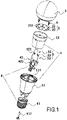
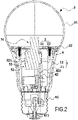
- an intelligent lamp provided by an embodiment includes a heat dissipation element 1 having a hollow structure inside, a cover element 3 disposed to cover a side of the heat dissipation element 1, a lamp holder assembly 4 disposed at another side of the heat dissipation element 1, a light source module 2 disposed in the heat dissipation element 1 and electrically connected to the lamp holder assembly 4, and a communications module 5 disposed through the light source module 2 and electrically connected to the lamp holder assembly 4.
- the light source module 2 includes a light source board 21 disposed in the heat dissipation element 1.
- the communications module 5 includes an antenna 51 and a radio frequency (RF) module 52 disposed at two opposite sides of the light source board 21.
- RF radio frequency
- the light source board 21 may separate the antenna 51 and the RF module 52 into two areas where the RF module 52 may be in a cavity area formed by the light source board 21 and the heat dissipation element 1, and the antenna 51 may extend beyond the light source board 21.
- a plurality of ground components 521 are disposed on the RF module 52 and the ground components 521 may conductively contact the light source board 21.
- the RF module 52 is coupled to the light source board 21 via the ground components 521 so that a ground of the antenna 51 (i.e. a ground of the RF module 52) is coupled to the light source board 21.
- this design concept is applicable to products related to lamps such as bulb devices, and also feasible for related products including an RF module (e.g., the RF module 52) and an antenna (e.g., the antenna 51).
- the light source board 21 and the RF module 52 are coupled via the ground components 521, the ground of the antenna 51, the ground of the RF module 52, the light source board 21 and the heat dissipation element 1 are integrated. Compared with a design of prior art, there are some improvements as follows.
- the heat dissipation element 1 and the cover element 3 may cover the light source module 2 and the communications module 5 inside to protect them.
- the heat dissipation element 1 may include an insulation layer 11 and a heat dissipation layer 12 disposed from an outer position to an inner position in order, where the inner position may be closer to the light source board 21.
- the heat dissipation layer 12 may be made of aluminum.
- the aluminum heat dissipation element 1 may dissipate heat and have a relatively higher conductivity.
- the insulation layer 11 may be disposed outside the heat dissipation layer 12 to avoid electric shock when touched by a human hand.
- the heat dissipation layer 12 may form a cylinder with two ends open.
- the insulation layer may form a cup body with two ends open.
- the light source board 21 may cover on the heat dissipation layer 12 and be fixed using connection elements such as the screws 6.
- the heat dissipation layer 12 may support and fix the light source board 21.
- the cover element 3 may have a shape of a bulb.
- the cover element 3 may be formed using a transparent material such as a polycarbonate (PC) or a polyethylene terephthalate (PET) plastic material, so that a high transmittance can be assured, and the light can be emitted evenly.
- the cover element 3 may be engaged with the insulation layer 11 at the outer position.
- the cover element 3 may include a bulb part 31 and a buckle 32 where the buckle 32 may be bent toward the insulation layer 11 from a circumferential portion at an end of the bulb part 31.
- a circumferential portion of the insulation layer 11 may have a clamping groove 111 corresponding to the buckle 32.
- the buckle 32 and the clamping groove 111 may be used to be attached and detached with each other.
- the fit clearance between the cover element 3 and the insulation layer 11 may be substantially between 0 mm to 0.3 mm (millimeters), and there may be no requirement for thickness difference.
- a fit clearance between the cover element 3 and the insulation layer 11 may be substantially 0 mm, 0.1 mm, 0.2 mm or 0.3 mm.
- the lamp holder assembly 4 may include a lamp holder 41 and a driver element 42.
- the driver element 42 may be coupled between the lamp holder 41 and the light source board 21.
- the RF module 52 may be coupled to the driver element 42 by insertion.
- the communications module 5 includes a printed circuit board (PCB) 53 where the antenna 51 and the RF module 52 are disposed on the PCB 53.
- the RF module 52 and the antenna 51 may be coupled to one another via the feeding wires (not illustrated) of the PCB 53.
- the driver element 42 may include a driver board 421 and components located on the driver board 421.
- the PCB 53 and the driver board 421 may be coupled by being orthogonally inserted, so that the lamp holder 41 may be electrically connected with the PCB 53 via the driver board 421.
- the ground component 521 may be disposed on the PCB 53, and the ground component 521 may conductively contact the light source board 21.
- an end of the lamp holder 41 may be attached with the insulation layer at an outer position by screwing. Another end of the lamp holder 41 may be electrically connected to an external power source through a pin 411 located inside.
- the pin 411 may be used to provide currents for the RF module 52 and the light source module 2 respectively through the driver element 42.
- the fir clearance between the lamp holder 41 and the insulation layer 11 may be substantially between 0 mm to 0.2 mm without requirement for thickness difference. According to an embodiment, the fir clearance between the lamp holder 41 and the insulation layer 11 may be substantially 0 mm, 0.1 mm or 0.2 mm.
- an output connector 422 may be disposed on the driver element 42.
- An input connector (not illustrated) electrically connected to the output connector 422 may be disposed on the light source board 21.
- the light source board 21 may have a through hole 211, and the output connector 422 may be electrically connected to the output connector via the through hole 211.
- the output connector 422 may be a male connector, and the input connector may be a female connector.
- the output connector 422 may be a female connector, and the input connector may be a female connector.
- the types of the output connector 422 and the input connector may be not limited as long as the two connectors can be connected.
- the light source module 2 may further include at least one light-emitting diode (LED) light source 22 disposed on the light source board 21.
- the driver element 42 may be electrically connected to the LED light source 22 and be used to drive the LED light source 11 to emit light.
- one of the ground components 521 includes a spring leaf coupled between the RF module 52 and the light source board 21.
- a portion of the spring leaf may be coupled to the PCB 53, and another portion of the spring leaf is coupled to the light source board 21.
- the spring leaf may have a straight shape.
- the spring leaf with a straight shape may be coupled to the PCB 53 and the light source board 21 respectively through an adhesive (e.g., an electrically conductive adhesive) or a connection element as long as the spring leaf can be fixed and kept conductive so as to have a conductive path between the PCB 53 and the light source board 21.
- an adhesive e.g., an electrically conductive adhesive
- the spring leaf may have an arc shape, and be connected in a way that a straight-shaped spring leaf is connected as described above.
- a curvature of an arc-shaped spring leaf is larger, two installation holes may be respectively opened for two ends of the arc-shaped spring leaf for the spring leaf to be connected between the PCB 53 and the light source board 21 through a connection element.
- the spring leaf may have a bent shape.
- the spring leaf may have a first bent portion 5211, a connecting portion 5213 and a second bent portion 5212.
- the first bent portion 5211 may be coupled to the light source board 21.
- the second bent portion 5212 may be coupled to the PCB 53.
- the first bent portion 5211 may be extended from an end of the connecting portion 5213 toward a side of the light source board 21.
- the second bent portion 5212 may be extended from an end of the connecting portion 5213 toward a side of the PCB 53.
- the bent portions 5211 and 5212 may be optionally bent.
- the connecting portion 5213 may have a bent shape or an arc shape.
- the first bent portion 5211, the second bend portion 5212 and the connecting portion 5213 may be of an integrally formed structure, where the integrally formed structure is preferably to be made of a same material.
- the abovementioned spring leaf may be a ground connector coupled between the light source board 21 and the RF module 52.
- a connector may be a terminal which is a component used to realize electrical connection and be of the industrial category of the connectors.
- the said connectors may include a male connector disposed on the light source board 21 and a female connector disposed on the PCB 53, where the male connector may be inserted into the female connector to conductively connect the light source board 21 and the PCB 53.
- a male connector may be disposed on the PCB 53, and a female connector may be disposed on the light source board 21.
- the ground component 521 may be used to conductively connect the light source board 21 and the RF module 52 by contacting a portion where the oxide layer is removed.
- a copper exposed area 212 may be disposed on the light source board 21, and the said ground components 521 may conductively contact the copper exposed area 212.
- a portion of the light source board 21 being close to the ground component 521 may be processed by laser engraving or oxide removing to make the portion conductive, so the RF module 52 and the light source board 21 may be conductively connected. The whole lamp may be operated as a portion of the antenna 51, and the antenna 51 may radiate more effectively.
- a previous antenna Compared with a previous antenna design, a previous antenna has to avoid a metal surface to avoid antenna affects, and transmission efficiency is reduced.
- metal parts close to the RF module 52 and the whole lamp may be integrated, the lamp may be used as a part of the antenna 51, so it is not necessary to avoid the metal parts, and the metal parts can be used for radiation.
- power may be provided to the LED light source 22 via the path described below.
- the alternating current (AC) power from an external power source may be sent through the pin 411 of the lamp holder 41 to the driver element 42. Then, the power may be sent through the output connector 422 and the input connected coupled with the output connector 422 to the light source board 21, and the current may be sent to the LED light source.
- AC alternating current
- Power may be provided to the antenna 51 via the path described below.
- the alternating current (AC) power from an external power source may be sent through the pin 411 of the lamp holder 41 to the driver element 42. Then, the power may be sent to the PCB 53. The power may be sent to the antenna 51 through the feeding wires.
- AC alternating current
- the communications module may control the light source module via the path described below.
- the antenna 51 may receive a control signal, and send the control signal to the RF module 52.
- the RF module 52 may control the driver element 42 according to the control signal to drive the LED light source 22 to emit light.
Landscapes
- Engineering & Computer Science (AREA)
- General Engineering & Computer Science (AREA)
- Microelectronics & Electronic Packaging (AREA)
- Physics & Mathematics (AREA)
- Optics & Photonics (AREA)
- Computer Networks & Wireless Communication (AREA)
- Non-Portable Lighting Devices Or Systems Thereof (AREA)
- Arrangement Of Elements, Cooling, Sealing, Or The Like Of Lighting Devices (AREA)
- Support Of Aerials (AREA)
Claims (10)
- Intelligente Lampe, umfassend:ein Wärmeableitungselement (1) mit einer hohlen Struktur im Inneren;ein Abdeckelement (3), das angeordnet ist, um eine Seite des Wärmeableitungselements (1) abzudecken;eine Lampenfassungsanordnung (4), die an einer anderen Seite des Wärmeableitungselements (1) angeordnet ist;ein Lichtquellenmodul (2), das in dem Wärmeableitungselement (1) angeordnet ist, elektrisch mit der Lampenfassungsanordnung (4) verbunden ist und eine Lichtquellenplatine (21) umfasst, die in dem Wärmeableitungselement (1) angeordnet ist; undein Kommunikationsmodul (5), das durch das Lichtquellenmodul (2) angeordnet ist, elektrisch mit der Lampenfassungsanordnung (4) verbunden ist, und wobei das Kommunikationsmodul (5) eine Antenne (51) und ein Hochfrequenzmodul (52) umfasst, die an zwei gegenüberliegenden Seiten der Lichtquellenplatine (21) angeordnet sind, wobei eine Vielzahl von Erdungskomponenten (521) auf dem Hochfrequenzmodul (52) angeordnet sind und die Erdungskomponenten (521) die Lichtquellenplatine (21) kontaktieren,wobei die Lichtquellenplatine (21), das Hochfrequenzmodul (25) und das Wärmeableitungselement (1) über die Erdungskomponenten (521) miteinander gekoppelt sind, und eine Erdung der Antenne (51), eine Erdung des Hochfrequenzmoduls (52), eine Erdung der Lichtquellenplatine (21) und das Wärmeableitungselement (1) elektrisch verbunden sind, um das Wärmeableitungselement (1) zu einem Teil der Antenne (51) zu machen,ein freigelegter Kupferbereich (212) auf der Lichtquellenplatine (21) angeordnet ist und die Erdungskomponenten den freigelegten Kupferbereich (212) kontaktieren,eine der Erdungskomponenten ein Federblatt umfasst, das zwischen das Hochfrequenzmodul (52) und die Lichtquellenplatine (21) gekoppelt ist,die Antenne (51) und das Hochfrequenzmodul (52) auf einer PCB (53) angeordnet sind, undein Abschnitt des Federblatts kann mit der PCB (53) gekoppelt sein und ein anderer Abschnitt des Federblatts mit der Lichtquellenplatine (21) gekoppelt ist.
- Intelligente Lampe nach Anspruch 1, wobei das Federblatt eine gerade Form hat.
- Intelligente Lampe nach Anspruch 1, wobei das Federblatt eine Bogenform hat.
- Intelligente Lampe nach Anspruch 1, wobei das Federblatt eine gebogene Form hat.
- Intelligente Lampe nach einem der Ansprüche 1 bis 4, wobei die Lampenfassungsanordnung (4) ferner umfasst:eine mit dem Wärmeableitungselement gekoppelte Lampenfassung (41); undein Treiberelement (42), das zwischen der Lampenfassung und die Lichtquellenplatine gekoppelt ist.
- Intelligente Lampe nach Anspruch 1, wobei eine der Erdungskomponenten einen Verbinder umfasst, der zwischen das Hochfrequenzmodul (52) und die Lichtquellenplatine (21) gekoppelt ist.
- Intelligente Lampe nach Anspruch 6, wobei ein freigelegter Kupferbereich auf der Lichtquellenplatine angeordnet ist, und die Erdungskomponenten den freigelegten Kupferbereich kontaktieren.
- Intelligente Lampe nach Anspruch 6, wobei die Lampenfassungsanordnung ferner umfasst:eine mit dem Wärmeableitungselement gekoppelte Lampenfassung; undein Treiberelement, das zwischen der Lampenfassung und die Lichtquellenplatine gekoppelt ist.
- Intelligente Lampe nach Anspruch 8, wobei das Lichtquellenmodul (2) ferner umfasst:mindestens eine Leuchtdioden-Lichtquelle, die auf der Lichtquellenplatine (21) angeordnet ist;wobei das Treiberelement (42) elektrisch mit der Leuchtdioden-Lichtquelle (22) verbunden und konfiguriert ist, um die Leuchtdioden-Lichtquelle (11) anzusteuern.
- Intelligente Lampe nach Anspruch 8, wobei das Wärmeableitungselement (1) ferner umfasst:eine Wärmeableitungsschicht (12), wobei die Lichtquellenplatine (21) angeordnet ist, um einen Abschnitt der Wärmeableitungsschicht (12) zu bedecken; undeine Isolationsschicht (11), wobei die Lampenfassung mit einem Abschnitt der Isolationsschicht (11) verschraubt ist;wobei die Wärmeableitungsschicht (12) und die Isolationsschicht (11) der Reihe nach von einer inneren Position zu einer äußeren Position angeordnet sind.
Applications Claiming Priority (1)
| Application Number | Priority Date | Filing Date | Title |
|---|---|---|---|
| CN201920290327.5U CN209672089U (zh) | 2019-03-07 | 2019-03-07 | 一种智能灯 |
Publications (2)
| Publication Number | Publication Date |
|---|---|
| EP3705772A1 EP3705772A1 (de) | 2020-09-09 |
| EP3705772B1 true EP3705772B1 (de) | 2022-04-20 |
Family
ID=68570817
Family Applications (1)
| Application Number | Title | Priority Date | Filing Date |
|---|---|---|---|
| EP20161361.9A Active EP3705772B1 (de) | 2019-03-07 | 2020-03-06 | Intelligente lampe mit lichtquellenmodul und kommunikationsmodul |
Country Status (3)
| Country | Link |
|---|---|
| US (1) | US11174997B2 (de) |
| EP (1) | EP3705772B1 (de) |
| CN (1) | CN209672089U (de) |
Families Citing this family (4)
| Publication number | Priority date | Publication date | Assignee | Title |
|---|---|---|---|---|
| CN214580954U (zh) * | 2021-02-24 | 2021-11-02 | 漳州立达信光电子科技有限公司 | 一种led灯具 |
| CN116111344B (zh) * | 2022-03-10 | 2025-11-04 | 漳州立达信光电子科技有限公司 | 智能灯 |
| CN114963036A (zh) * | 2022-06-21 | 2022-08-30 | 深圳市水世界信息有限公司 | 一种智能球泡灯 |
| CN222543784U (zh) * | 2024-06-11 | 2025-02-28 | 厦门通士达照明有限公司 | 一种基于dob设计的多色温切换led灯 |
Citations (2)
| Publication number | Priority date | Publication date | Assignee | Title |
|---|---|---|---|---|
| WO2014140961A1 (en) * | 2013-03-13 | 2014-09-18 | Koninklijke Philips N.V. | A lighting device and luminaire comprising an antenna. |
| KR20150129388A (ko) * | 2014-05-12 | 2015-11-20 | 엘지전자 주식회사 | 조명 장치 |
Family Cites Families (8)
| Publication number | Priority date | Publication date | Assignee | Title |
|---|---|---|---|---|
| TW201250154A (en) * | 2012-07-23 | 2012-12-16 | Kenner Material & System Co Ltd | Structure of plastic heat sink for LED bulb and method of making the same |
| KR102015911B1 (ko) * | 2012-11-12 | 2019-08-29 | 엘지전자 주식회사 | 조명장치 |
| KR20150109656A (ko) * | 2014-03-20 | 2015-10-02 | 엘지이노텍 주식회사 | 조명 장치 |
| US9538623B2 (en) * | 2014-05-12 | 2017-01-03 | Lg Electronics Inc. | Lighting device |
| US9488352B2 (en) * | 2014-05-28 | 2016-11-08 | Technical Consumer Products, Inc. | Radio frequency (RF) signal pathway for a lamp antenna |
| US10129960B2 (en) * | 2014-11-10 | 2018-11-13 | Cree, Inc. | Antenna arrangement for a solid-state lamp |
| CN105444008B (zh) * | 2015-11-30 | 2018-10-19 | 小米科技有限责任公司 | 一种智能灯 |
| CN206682674U (zh) * | 2017-04-14 | 2017-11-28 | 漳州立达信光电子科技有限公司 | 一种智能灯具 |
-
2019
- 2019-03-07 CN CN201920290327.5U patent/CN209672089U/zh active Active
-
2020
- 2020-03-06 EP EP20161361.9A patent/EP3705772B1/de active Active
- 2020-03-06 US US16/811,993 patent/US11174997B2/en active Active
Patent Citations (2)
| Publication number | Priority date | Publication date | Assignee | Title |
|---|---|---|---|---|
| WO2014140961A1 (en) * | 2013-03-13 | 2014-09-18 | Koninklijke Philips N.V. | A lighting device and luminaire comprising an antenna. |
| KR20150129388A (ko) * | 2014-05-12 | 2015-11-20 | 엘지전자 주식회사 | 조명 장치 |
Also Published As
| Publication number | Publication date |
|---|---|
| EP3705772A1 (de) | 2020-09-09 |
| CN209672089U (zh) | 2019-11-22 |
| US20200284400A1 (en) | 2020-09-10 |
| US11174997B2 (en) | 2021-11-16 |
Similar Documents
| Publication | Publication Date | Title |
|---|---|---|
| US11174997B2 (en) | Intelligent lamp including light source module and communications module | |
| KR101999660B1 (ko) | 통신 모듈을 포함하는 조명 장치 | |
| JP6334437B2 (ja) | 照明装置 | |
| CN205065392U (zh) | 照明器具 | |
| US9538623B2 (en) | Lighting device | |
| US8556462B2 (en) | LED lighting device | |
| US20050169006A1 (en) | Led chip lamp apparatus | |
| CN104566027B (zh) | Led照明装置、系统及其天线布置方法 | |
| CN101165396A (zh) | 半导体灯 | |
| EP2077415B1 (de) | LED-Lampe mit Wärmeabfuhrvorrichtung | |
| KR20090006633U (ko) | 엘이디램프 모듈 연결구조 | |
| US6799870B2 (en) | Sideway-projecting light emitting diode structure | |
| US20150003080A1 (en) | Light emitting diode module | |
| CN211925426U (zh) | 一种智能灯 | |
| US20160169484A1 (en) | Lighting device | |
| CN212960971U (zh) | 智能灯 | |
| CN103579750B (zh) | 移动装置 | |
| KR102059342B1 (ko) | 조명 장치 | |
| KR101512499B1 (ko) | 비용절감형 인쇄회로기판 및 이를 이용한 led 조명장치 | |
| US20150123559A1 (en) | Optical semiconductor lighting apparatus | |
| CN204328571U (zh) | Led照明装置及系统 | |
| CN113067118B (zh) | 照明装置 | |
| US10869418B2 (en) | Lamp | |
| CN102667306A (zh) | 具有共同模制的金属触头的发光二极管照明模块 | |
| CN102447184A (zh) | 连接器及照明装置 |
Legal Events
| Date | Code | Title | Description |
|---|---|---|---|
| PUAI | Public reference made under article 153(3) epc to a published international application that has entered the european phase |
Free format text: ORIGINAL CODE: 0009012 |
|
| STAA | Information on the status of an ep patent application or granted ep patent |
Free format text: STATUS: REQUEST FOR EXAMINATION WAS MADE |
|
| 17P | Request for examination filed |
Effective date: 20200306 |
|
| AK | Designated contracting states |
Kind code of ref document: A1 Designated state(s): AL AT BE BG CH CY CZ DE DK EE ES FI FR GB GR HR HU IE IS IT LI LT LU LV MC MK MT NL NO PL PT RO RS SE SI SK SM TR |
|
| AX | Request for extension of the european patent |
Extension state: BA ME |
|
| STAA | Information on the status of an ep patent application or granted ep patent |
Free format text: STATUS: EXAMINATION IS IN PROGRESS |
|
| 17Q | First examination report despatched |
Effective date: 20200918 |
|
| GRAP | Despatch of communication of intention to grant a patent |
Free format text: ORIGINAL CODE: EPIDOSNIGR1 |
|
| STAA | Information on the status of an ep patent application or granted ep patent |
Free format text: STATUS: GRANT OF PATENT IS INTENDED |
|
| RIC1 | Information provided on ipc code assigned before grant |
Ipc: F21Y 115/10 20160101ALN20211029BHEP Ipc: F21V 23/00 20150101ALI20211029BHEP Ipc: F21K 9/238 20160101ALI20211029BHEP Ipc: F21V 23/04 20060101ALI20211029BHEP Ipc: F21K 9/232 20160101AFI20211029BHEP |
|
| INTG | Intention to grant announced |
Effective date: 20211206 |
|
| GRAS | Grant fee paid |
Free format text: ORIGINAL CODE: EPIDOSNIGR3 |
|
| GRAA | (expected) grant |
Free format text: ORIGINAL CODE: 0009210 |
|
| STAA | Information on the status of an ep patent application or granted ep patent |
Free format text: STATUS: THE PATENT HAS BEEN GRANTED |
|
| AK | Designated contracting states |
Kind code of ref document: B1 Designated state(s): AL AT BE BG CH CY CZ DE DK EE ES FI FR GB GR HR HU IE IS IT LI LT LU LV MC MK MT NL NO PL PT RO RS SE SI SK SM TR |
|
| REG | Reference to a national code |
Ref country code: GB Ref legal event code: FG4D |
|
| REG | Reference to a national code |
Ref country code: CH Ref legal event code: EP |
|
| REG | Reference to a national code |
Ref country code: IE Ref legal event code: FG4D |
|
| REG | Reference to a national code |
Ref country code: DE Ref legal event code: R096 Ref document number: 602020002702 Country of ref document: DE |
|
| REG | Reference to a national code |
Ref country code: AT Ref legal event code: REF Ref document number: 1485403 Country of ref document: AT Kind code of ref document: T Effective date: 20220515 |
|
| REG | Reference to a national code |
Ref country code: LT Ref legal event code: MG9D |
|
| REG | Reference to a national code |
Ref country code: NL Ref legal event code: MP Effective date: 20220420 |
|
| REG | Reference to a national code |
Ref country code: AT Ref legal event code: MK05 Ref document number: 1485403 Country of ref document: AT Kind code of ref document: T Effective date: 20220420 |
|
| PG25 | Lapsed in a contracting state [announced via postgrant information from national office to epo] |
Ref country code: NL Free format text: LAPSE BECAUSE OF FAILURE TO SUBMIT A TRANSLATION OF THE DESCRIPTION OR TO PAY THE FEE WITHIN THE PRESCRIBED TIME-LIMIT Effective date: 20220420 |
|
| PG25 | Lapsed in a contracting state [announced via postgrant information from national office to epo] |
Ref country code: SE Free format text: LAPSE BECAUSE OF FAILURE TO SUBMIT A TRANSLATION OF THE DESCRIPTION OR TO PAY THE FEE WITHIN THE PRESCRIBED TIME-LIMIT Effective date: 20220420 Ref country code: PT Free format text: LAPSE BECAUSE OF FAILURE TO SUBMIT A TRANSLATION OF THE DESCRIPTION OR TO PAY THE FEE WITHIN THE PRESCRIBED TIME-LIMIT Effective date: 20220822 Ref country code: NO Free format text: LAPSE BECAUSE OF FAILURE TO SUBMIT A TRANSLATION OF THE DESCRIPTION OR TO PAY THE FEE WITHIN THE PRESCRIBED TIME-LIMIT Effective date: 20220720 Ref country code: LT Free format text: LAPSE BECAUSE OF FAILURE TO SUBMIT A TRANSLATION OF THE DESCRIPTION OR TO PAY THE FEE WITHIN THE PRESCRIBED TIME-LIMIT Effective date: 20220420 Ref country code: HR Free format text: LAPSE BECAUSE OF FAILURE TO SUBMIT A TRANSLATION OF THE DESCRIPTION OR TO PAY THE FEE WITHIN THE PRESCRIBED TIME-LIMIT Effective date: 20220420 Ref country code: GR Free format text: LAPSE BECAUSE OF FAILURE TO SUBMIT A TRANSLATION OF THE DESCRIPTION OR TO PAY THE FEE WITHIN THE PRESCRIBED TIME-LIMIT Effective date: 20220721 Ref country code: FI Free format text: LAPSE BECAUSE OF FAILURE TO SUBMIT A TRANSLATION OF THE DESCRIPTION OR TO PAY THE FEE WITHIN THE PRESCRIBED TIME-LIMIT Effective date: 20220420 Ref country code: ES Free format text: LAPSE BECAUSE OF FAILURE TO SUBMIT A TRANSLATION OF THE DESCRIPTION OR TO PAY THE FEE WITHIN THE PRESCRIBED TIME-LIMIT Effective date: 20220420 Ref country code: BG Free format text: LAPSE BECAUSE OF FAILURE TO SUBMIT A TRANSLATION OF THE DESCRIPTION OR TO PAY THE FEE WITHIN THE PRESCRIBED TIME-LIMIT Effective date: 20220720 Ref country code: AT Free format text: LAPSE BECAUSE OF FAILURE TO SUBMIT A TRANSLATION OF THE DESCRIPTION OR TO PAY THE FEE WITHIN THE PRESCRIBED TIME-LIMIT Effective date: 20220420 |
|
| PG25 | Lapsed in a contracting state [announced via postgrant information from national office to epo] |
Ref country code: RS Free format text: LAPSE BECAUSE OF FAILURE TO SUBMIT A TRANSLATION OF THE DESCRIPTION OR TO PAY THE FEE WITHIN THE PRESCRIBED TIME-LIMIT Effective date: 20220420 Ref country code: PL Free format text: LAPSE BECAUSE OF FAILURE TO SUBMIT A TRANSLATION OF THE DESCRIPTION OR TO PAY THE FEE WITHIN THE PRESCRIBED TIME-LIMIT Effective date: 20220420 Ref country code: LV Free format text: LAPSE BECAUSE OF FAILURE TO SUBMIT A TRANSLATION OF THE DESCRIPTION OR TO PAY THE FEE WITHIN THE PRESCRIBED TIME-LIMIT Effective date: 20220420 Ref country code: IS Free format text: LAPSE BECAUSE OF FAILURE TO SUBMIT A TRANSLATION OF THE DESCRIPTION OR TO PAY THE FEE WITHIN THE PRESCRIBED TIME-LIMIT Effective date: 20220820 |
|
| REG | Reference to a national code |
Ref country code: DE Ref legal event code: R097 Ref document number: 602020002702 Country of ref document: DE |
|
| PG25 | Lapsed in a contracting state [announced via postgrant information from national office to epo] |
Ref country code: SM Free format text: LAPSE BECAUSE OF FAILURE TO SUBMIT A TRANSLATION OF THE DESCRIPTION OR TO PAY THE FEE WITHIN THE PRESCRIBED TIME-LIMIT Effective date: 20220420 Ref country code: SK Free format text: LAPSE BECAUSE OF FAILURE TO SUBMIT A TRANSLATION OF THE DESCRIPTION OR TO PAY THE FEE WITHIN THE PRESCRIBED TIME-LIMIT Effective date: 20220420 Ref country code: RO Free format text: LAPSE BECAUSE OF FAILURE TO SUBMIT A TRANSLATION OF THE DESCRIPTION OR TO PAY THE FEE WITHIN THE PRESCRIBED TIME-LIMIT Effective date: 20220420 Ref country code: EE Free format text: LAPSE BECAUSE OF FAILURE TO SUBMIT A TRANSLATION OF THE DESCRIPTION OR TO PAY THE FEE WITHIN THE PRESCRIBED TIME-LIMIT Effective date: 20220420 Ref country code: DK Free format text: LAPSE BECAUSE OF FAILURE TO SUBMIT A TRANSLATION OF THE DESCRIPTION OR TO PAY THE FEE WITHIN THE PRESCRIBED TIME-LIMIT Effective date: 20220420 Ref country code: CZ Free format text: LAPSE BECAUSE OF FAILURE TO SUBMIT A TRANSLATION OF THE DESCRIPTION OR TO PAY THE FEE WITHIN THE PRESCRIBED TIME-LIMIT Effective date: 20220420 |
|
| PLBE | No opposition filed within time limit |
Free format text: ORIGINAL CODE: 0009261 |
|
| STAA | Information on the status of an ep patent application or granted ep patent |
Free format text: STATUS: NO OPPOSITION FILED WITHIN TIME LIMIT |
|
| 26N | No opposition filed |
Effective date: 20230123 |
|
| PG25 | Lapsed in a contracting state [announced via postgrant information from national office to epo] |
Ref country code: AL Free format text: LAPSE BECAUSE OF FAILURE TO SUBMIT A TRANSLATION OF THE DESCRIPTION OR TO PAY THE FEE WITHIN THE PRESCRIBED TIME-LIMIT Effective date: 20220420 |
|
| PG25 | Lapsed in a contracting state [announced via postgrant information from national office to epo] |
Ref country code: SI Free format text: LAPSE BECAUSE OF FAILURE TO SUBMIT A TRANSLATION OF THE DESCRIPTION OR TO PAY THE FEE WITHIN THE PRESCRIBED TIME-LIMIT Effective date: 20220420 |
|
| REG | Reference to a national code |
Ref country code: DE Ref legal event code: R119 Ref document number: 602020002702 Country of ref document: DE |
|
| PG25 | Lapsed in a contracting state [announced via postgrant information from national office to epo] |
Ref country code: MC Free format text: LAPSE BECAUSE OF FAILURE TO SUBMIT A TRANSLATION OF THE DESCRIPTION OR TO PAY THE FEE WITHIN THE PRESCRIBED TIME-LIMIT Effective date: 20220420 |
|
| REG | Reference to a national code |
Ref country code: CH Ref legal event code: PL |
|
| REG | Reference to a national code |
Ref country code: BE Ref legal event code: MM Effective date: 20230331 |
|
| PG25 | Lapsed in a contracting state [announced via postgrant information from national office to epo] |
Ref country code: LU Free format text: LAPSE BECAUSE OF NON-PAYMENT OF DUE FEES Effective date: 20230306 |
|
| REG | Reference to a national code |
Ref country code: IE Ref legal event code: MM4A |
|
| PG25 | Lapsed in a contracting state [announced via postgrant information from national office to epo] |
Ref country code: LI Free format text: LAPSE BECAUSE OF NON-PAYMENT OF DUE FEES Effective date: 20230331 Ref country code: IT Free format text: LAPSE BECAUSE OF FAILURE TO SUBMIT A TRANSLATION OF THE DESCRIPTION OR TO PAY THE FEE WITHIN THE PRESCRIBED TIME-LIMIT Effective date: 20220420 Ref country code: IE Free format text: LAPSE BECAUSE OF NON-PAYMENT OF DUE FEES Effective date: 20230306 Ref country code: DE Free format text: LAPSE BECAUSE OF NON-PAYMENT OF DUE FEES Effective date: 20231003 Ref country code: CH Free format text: LAPSE BECAUSE OF NON-PAYMENT OF DUE FEES Effective date: 20230331 |
|
| PG25 | Lapsed in a contracting state [announced via postgrant information from national office to epo] |
Ref country code: BE Free format text: LAPSE BECAUSE OF NON-PAYMENT OF DUE FEES Effective date: 20230331 |
|
| PG25 | Lapsed in a contracting state [announced via postgrant information from national office to epo] |
Ref country code: BG Free format text: LAPSE BECAUSE OF FAILURE TO SUBMIT A TRANSLATION OF THE DESCRIPTION OR TO PAY THE FEE WITHIN THE PRESCRIBED TIME-LIMIT Effective date: 20220420 |
|
| PG25 | Lapsed in a contracting state [announced via postgrant information from national office to epo] |
Ref country code: BG Free format text: LAPSE BECAUSE OF FAILURE TO SUBMIT A TRANSLATION OF THE DESCRIPTION OR TO PAY THE FEE WITHIN THE PRESCRIBED TIME-LIMIT Effective date: 20220420 |
|
| PG25 | Lapsed in a contracting state [announced via postgrant information from national office to epo] |
Ref country code: CY Free format text: LAPSE BECAUSE OF FAILURE TO SUBMIT A TRANSLATION OF THE DESCRIPTION OR TO PAY THE FEE WITHIN THE PRESCRIBED TIME-LIMIT; INVALID AB INITIO Effective date: 20200306 |
|
| PG25 | Lapsed in a contracting state [announced via postgrant information from national office to epo] |
Ref country code: HU Free format text: LAPSE BECAUSE OF FAILURE TO SUBMIT A TRANSLATION OF THE DESCRIPTION OR TO PAY THE FEE WITHIN THE PRESCRIBED TIME-LIMIT; INVALID AB INITIO Effective date: 20200306 |
|
| PG25 | Lapsed in a contracting state [announced via postgrant information from national office to epo] |
Ref country code: TR Free format text: LAPSE BECAUSE OF FAILURE TO SUBMIT A TRANSLATION OF THE DESCRIPTION OR TO PAY THE FEE WITHIN THE PRESCRIBED TIME-LIMIT Effective date: 20220420 |
|
| PGFP | Annual fee paid to national office [announced via postgrant information from national office to epo] |
Ref country code: FR Payment date: 20251210 Year of fee payment: 7 |
|
| PGFP | Annual fee paid to national office [announced via postgrant information from national office to epo] |
Ref country code: GB Payment date: 20260107 Year of fee payment: 7 |