EP3703468B1 - Led-beleuchtungsvorrichtung zur verhinderung von flackern - Google Patents
Led-beleuchtungsvorrichtung zur verhinderung von flackern Download PDFInfo
- Publication number
- EP3703468B1 EP3703468B1 EP18871480.2A EP18871480A EP3703468B1 EP 3703468 B1 EP3703468 B1 EP 3703468B1 EP 18871480 A EP18871480 A EP 18871480A EP 3703468 B1 EP3703468 B1 EP 3703468B1
- Authority
- EP
- European Patent Office
- Prior art keywords
- current
- effect transistor
- terminal
- field
- constant
- Prior art date
- Legal status (The legal status is an assumption and is not a legal conclusion. Google has not performed a legal analysis and makes no representation as to the accuracy of the status listed.)
- Active
Links
Images





Classifications
-
- H—ELECTRICITY
- H05—ELECTRIC TECHNIQUES NOT OTHERWISE PROVIDED FOR
- H05B—ELECTRIC HEATING; ELECTRIC LIGHT SOURCES NOT OTHERWISE PROVIDED FOR; CIRCUIT ARRANGEMENTS FOR ELECTRIC LIGHT SOURCES, IN GENERAL
- H05B45/00—Circuit arrangements for operating light-emitting diodes [LED]
- H05B45/30—Driver circuits
- H05B45/345—Current stabilisation; Maintaining constant current
-
- H—ELECTRICITY
- H05—ELECTRIC TECHNIQUES NOT OTHERWISE PROVIDED FOR
- H05B—ELECTRIC HEATING; ELECTRIC LIGHT SOURCES NOT OTHERWISE PROVIDED FOR; CIRCUIT ARRANGEMENTS FOR ELECTRIC LIGHT SOURCES, IN GENERAL
- H05B45/00—Circuit arrangements for operating light-emitting diodes [LED]
-
- H—ELECTRICITY
- H05—ELECTRIC TECHNIQUES NOT OTHERWISE PROVIDED FOR
- H05B—ELECTRIC HEATING; ELECTRIC LIGHT SOURCES NOT OTHERWISE PROVIDED FOR; CIRCUIT ARRANGEMENTS FOR ELECTRIC LIGHT SOURCES, IN GENERAL
- H05B45/00—Circuit arrangements for operating light-emitting diodes [LED]
- H05B45/10—Controlling the intensity of the light
- H05B45/14—Controlling the intensity of the light using electrical feedback from LEDs or from LED modules
-
- H—ELECTRICITY
- H05—ELECTRIC TECHNIQUES NOT OTHERWISE PROVIDED FOR
- H05B—ELECTRIC HEATING; ELECTRIC LIGHT SOURCES NOT OTHERWISE PROVIDED FOR; CIRCUIT ARRANGEMENTS FOR ELECTRIC LIGHT SOURCES, IN GENERAL
- H05B45/00—Circuit arrangements for operating light-emitting diodes [LED]
- H05B45/30—Driver circuits
- H05B45/37—Converter circuits
- H05B45/3725—Switched mode power supply [SMPS]
-
- H—ELECTRICITY
- H05—ELECTRIC TECHNIQUES NOT OTHERWISE PROVIDED FOR
- H05B—ELECTRIC HEATING; ELECTRIC LIGHT SOURCES NOT OTHERWISE PROVIDED FOR; CIRCUIT ARRANGEMENTS FOR ELECTRIC LIGHT SOURCES, IN GENERAL
- H05B45/00—Circuit arrangements for operating light-emitting diodes [LED]
- H05B45/30—Driver circuits
- H05B45/395—Linear regulators
-
- H—ELECTRICITY
- H05—ELECTRIC TECHNIQUES NOT OTHERWISE PROVIDED FOR
- H05B—ELECTRIC HEATING; ELECTRIC LIGHT SOURCES NOT OTHERWISE PROVIDED FOR; CIRCUIT ARRANGEMENTS FOR ELECTRIC LIGHT SOURCES, IN GENERAL
- H05B45/00—Circuit arrangements for operating light-emitting diodes [LED]
- H05B45/40—Details of LED load circuits
- H05B45/44—Details of LED load circuits with an active control inside an LED matrix
- H05B45/48—Details of LED load circuits with an active control inside an LED matrix having LEDs organised in strings and incorporating parallel shunting devices
-
- H—ELECTRICITY
- H05—ELECTRIC TECHNIQUES NOT OTHERWISE PROVIDED FOR
- H05B—ELECTRIC HEATING; ELECTRIC LIGHT SOURCES NOT OTHERWISE PROVIDED FOR; CIRCUIT ARRANGEMENTS FOR ELECTRIC LIGHT SOURCES, IN GENERAL
- H05B45/00—Circuit arrangements for operating light-emitting diodes [LED]
- H05B45/50—Circuit arrangements for operating light-emitting diodes [LED] responsive to malfunctions or undesirable behaviour of LEDs; responsive to LED life; Protective circuits
- H05B45/59—Circuit arrangements for operating light-emitting diodes [LED] responsive to malfunctions or undesirable behaviour of LEDs; responsive to LED life; Protective circuits for reducing or suppressing flicker or glow effects
-
- Y—GENERAL TAGGING OF NEW TECHNOLOGICAL DEVELOPMENTS; GENERAL TAGGING OF CROSS-SECTIONAL TECHNOLOGIES SPANNING OVER SEVERAL SECTIONS OF THE IPC; TECHNICAL SUBJECTS COVERED BY FORMER USPC CROSS-REFERENCE ART COLLECTIONS [XRACs] AND DIGESTS
- Y02—TECHNOLOGIES OR APPLICATIONS FOR MITIGATION OR ADAPTATION AGAINST CLIMATE CHANGE
- Y02B—CLIMATE CHANGE MITIGATION TECHNOLOGIES RELATED TO BUILDINGS, e.g. HOUSING, HOUSE APPLIANCES OR RELATED END-USER APPLICATIONS
- Y02B20/00—Energy efficient lighting technologies, e.g. halogen lamps or gas discharge lamps
- Y02B20/30—Semiconductor lamps, e.g. solid state lamps [SSL] light emitting diodes [LED] or organic LED [OLED]
Definitions
- the present disclosure relates to an LED lighting device, and particularly to an LED lighting device for preventing a flicker that can reduce current ripples caused in an AC power supply of the LED lighting device by adjusting a constant current in a light-emitting unit, thereby preventing a flicker without increasing the number and capacity of electrolytic capacitors, preventing a deterioration of aesthetic qualities of the LED lighting device and easily satisfying the requirements of a performance certification program.
- a flicker of an LED light cannot be seen by people with their naked eyes but can be seen by cameras that can capture after images at a speed higher than that of the eyes of people.
- a flicker of an LED lighting device can occur periodically and can cause eye fatigue to users.
- FIG. 1 is a view illustrating a 23W-AC-driven LED lighting device for preventing a flicker of the related art.
- FIG. 2 is a circuit diagram illustrating the LED lighting device in FIG. 1 .
- the LED lighting device is provided with an AC power supply 10, a rectifying unit 20, first and second light-emitting units 30, 40, and a series-type switching unit 50.
- the first light-emitting unit 30 includes a first LED array (LA1), a first electrolytic capacitor (EC1) and a first discharge resistance (RC1)
- the second light-emitting unit 40 includes a second LED array (LA2), a second electrolytic capacitor (EC2) and a second discharge resistance (RC2).
- FIG. 3 is a graph illustrating a waveform of a sine wave of an AC voltage output from an AC power supply 10 in the LED lighting device in FIG. 2 .
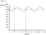
- FIG. 4 is a graph illustrating a waveform as a result of simulation of electric currents and ripple currents flowing in a first LED array (LA1) in the LED lighting device in FIG. 2 .
- An AC component takes the form of a sinusoidal voltage that is twice as high as a frequency of an AC voltage from a main line or a power supply similar to the main line.
- An LED that is a diode shows a low differential impedance that is defined as a change rate of a voltage to an electric current in its operation section.
- the low differential impedance causes a significant amount of ripple current of the LED when there are voltage ripples.
- the ripples are generated at a frequency twice as high as an AC frequency of a main line, which is between 100 Hz and 120 Hz.
- the flicker is caused when current ripples occur in an LED lighting device.
- the current ripples can cause a flicker of light.
- LED technologies are limitedly applied to lighting in households, offices, streets and industries.
- the study shows that about 75 % of healthy adults have sensitivity to the stroboscopic phenomenon due to a 10 % flicker that is caused by about 20 % of current ripples at a frequency of 100 Hz.
- LED lighting Due to sensitivity to the stroboscopic phenomenon caused by a flicker, LED lighting is not widely used for applications in which comfortable and accurate recognition of movements is an important factor, and applications in which an illuminated scene includes movement, vibration or rotation of an object.
- a dimming device of an LED lamp of the related art using a triac dimmer changes an output voltage corresponding to an amount of changes at a constant ratio even when a phase angle used for determining a dimming range is fixed.
- a flicker has no option but to occur to an LED of the lamp driven by an AC power supply 10.
- a forward-direction voltage of a predetermined level has to be input.
- the AC voltage is changed at a constant ratio due to the external environment into a voltage lower than or equal to a critical value (a threshold voltage).
- the threshold voltage is usually changed in a range of low voltages.
- capacitance supplied to an output of the power supply device or output near the output value of the power supply device is used to smooth voltage ripples generated by the power supply device, preferably, to lower the voltage ripples to a level of a few percents.
- an LED lighting apparatus used in streets, offices or industries in the form of a long series-connected string is considered effective, and each string is supplied with a constant direct current by a single driver.
- a DC output voltage of the driver needs to be high enough to drive a plurality of LEDs such that each driver guarantees generation of a sufficient amount of optical power from the LED string driven by the driver.
- an electric capacitor used to smooth voltage ripples from the power supply device has to tolerate a relatively high DC voltage such as 200 V or higher.
- electrolytic capacitor can tolerate a voltage as high as the above described voltage while supplying a high capacitance value of approximately hundreds of microfarads ( ⁇ F) unlike other types of capacitors.
- the number of capacitors used to realize total required capacitance is determined at least partially by a maximum rated ripple current with respect to each capacitor.
- the number and capacity of electrolytic capacitors required for output from the power supply device of an LED driver are preferably reduced.
- a peak-to-peak value of current ripples in an LED array preferably accounts for less than about 1 % of DC currents supplied to the LED array, and, on the basis of the peak-to-peak value, a flicker directly detectable and a flicker quantum stroboscopically detectable are preferably reduced significantly or removed.
- a power supply device designed to be used in an LED driver is required to achieve two opposite purposes sought by lighting used in streets, offices and industries.
- the power supply device supplies a low voltage ripple to minimize an LED current ripple and an optical flicker.
- Electric charge that charges first and second electrolytic capacitors (EC1 and EC2) is discharged through a voltage drop or a resistance in first and second LED arrays (LA1 and LA2).
- a large amount of electric currents flow and a large amount of electric charge is discharged.
- a flicker may occur more often at a low power level than a normal power level when brightness is adjusted using a triac dimmer.
- a capacitor having a capacity and size larger than a capacitor that satisfies a flicker at a normal power level has to be used to satisfy the standard of a flicker at a low power level.
- the Energy Star is a program for certifying performance of a product, which is presented by the US government to encourage consumers to use energy efficient products, and is well known for its logo on various electronic devices such as computers, peripheral devices, lighting devices and the like.
- a speed of charge and discharge in a normal state is based on a time constant defined by multiplying a dynamic resistance (R_LAj) of each LED array (LAj) by capacitance (C_ECj) of each electrolytic capacitor (ECj).
- a fluctuation of a voltage at the time of charge is increased at a ratio of 1-exp (-R LAj x C_ECj) at a voltage right before the charge, and a fluctuation of a voltage at the time of discharge is decreased at a ratio of exp (-R LAj x C_ECj) at a voltage right before the discharge.
- the number of LED arrays (LAj) connected in series has to be halved and the LED arrays (LAj) have to be driven in parallel. Accordingly, a resistance has to be halved, a driving current has to be doubled, and a value of capacitance has to be quadrupled.
- volume of the electrolytic capacitor (ECj) has to be doubled when the LED lighting device is actually implemented.
- the capacitance As described above, has to be ten-folded. Also, the volume has to be ten-folded.
- percent flicker is measured at 10.5 %, as in the waveform of FIG. 5 .
- KR 101 778 494 B1 discloses an apparatus for light controller both AC and DC with flicker removal function.
- the present disclosure is directed to an LED lighting device for preventing a flicker that can reduce current ripples generated from an AC power supply of the LED lighting device by adjusting a constant current in a light-emitting unit, thereby making it possible to reduce a flicker without increasing the number and capacity of electrolytic capacitors.
- An LED lighting device for preventing a flicker includes; a rectifying unit configured to be supplied with an AC voltage from an AC power supply, configured to rectify the same and configured to output a direct current; a first light-emitting unit supplied with a part of the direct current, configured to adjust a first constant current and configured to allow a first LED array to emit light; a second light-emitting unit supplied with a part of the adjusted first constant current, configured to adjust a second constant current and configured to allow a second LED array to emit light; and a series-type switching unit supplied with the remaining part of the direct current, the remaining part of the adjusted first constant current and the adjusted second constant current and configured to control delivery of the remaining part of the direct current, the remaining part of the adjusted first constant current and the adjusted second constant current on the basis of opening and closing of a plurality of transistors built into the series-type switching unit, wherein the current supplied to the first light-emitting unit is supplied by passing through a first di
- the first light-emitting unit of an LED lighting device for preventing a flicker comprises: a first electrolytic capacitor with one side connected to a cathode terminal of the first diode and the other side connected to an anode terminal of the second diode to charge first electric charge; a first discharge resistance connected in parallel with the first electrolytic capacitor and configured to discharge the charged first electric charge; the first LED array being provided with a plurality of LEDs, supplied with a part of the current having passed through the first diode and configured to emit light; and a first constant-current adjusting unit with one side connected to an output terminal of the first LED array and the other side connected to the anode terminal of the second diode to adjust and output the first constant current.
- the first constant-current adjusting unit of an LED lighting device for preventing a flicker comprises: a first field-effect transistor having a drain terminal connected to the output terminal of the first LED array and being configured to switch a flow of the first constant current; a first drain resistance with one side connected to the drain terminal of the first field-effect transistor and the other side connected to a gate terminal of the first field-effect transistor to adjust a gate bias; a first current-branch resistance with one side connected to the drain terminal of the first field-effect transistor and the other side connected to a source terminal of the first field-effect transistor to branch a drain current of the first field-effect transistor; a first current-control resistance with one side connected to the source terminal of the first field-effect transistor and the other side connected to the anode terminal of the second diode to control a source current of the first field-effect transistor; a first gate resistance with one side connected to the gate terminal of the first field-effect transistor and the other side connected to the anode terminal of the second diode to adjust the gate
- the second light-emitting unit of an LED lighting device for preventing a flicker comprises: a second electrolytic capacitor with one side connected to a cathode terminal of the second diode to charge second electric charge; a second discharge resistance connected in parallel with the second electrolytic capacitor and configured to discharge the charged second electric charge; the second LED array being provided with a plurality of LEDs, supplied with a part of the current having passed through the second diode and configured to emit light; and a second constant-current adjusting unit with one side connected to an output terminal of the second LED array to adjust and output the second constant current.
- the second constant-current adjusting unit of an LED lighting device for preventing a flicker comprises: a second field-effect transistor having a drain terminal connected to an output terminal of the second LED array and being configured to switch a flow of the second constant current; a second drain resistance with one side connected to the drain terminal of the second field-effect transistor and the other side connected to a gate terminal of the second field-effect transistor to adjust a gate bias; a second current-branch resistance with one side connected to the drain terminal of the second field-effect transistor and the other side connected to a source terminal of the second field-effect transistor to branch a drain current of the second field-effect transistor; a second current-control resistance with one side connected to the source terminal of the second field-effect transistor and the other side connected to the series-type switching unit to control a source current of the second field-effect transistor; a second gate resistance with one side connected to the gate terminal of the second field-effect transistor and the other side connected to the series-type switching unit to adjust the gate bias; and a second gate-voltage
- the series-type switching unit of an LED lighting device for preventing a flicker comprising: a power-supply resistance, one side of which is connected to the rectifying unit, which is supplied with the remaining part of direct current and which is supplied with a constant voltage; first to third branch resistances which are connected in series, one side of which is connected to the other side of the power-supply resistance to receive the constant voltage, and the other side of which is grounded to branch the constant voltage; a Zener diode whose anode terminal is grounded, which is connected in parallel with the first to third branch resistances and which is configured to prevent an overvoltage; a first transistor whose gate terminal is connected to a contact point of the first and second branch resistances and whose drain terminal is supplied with the remaining part of the first constant current; and a second transistor whose gate terminal is connected to a contact point of the second and third branch resistances and whose drain terminal is supplied with the remaining part of the second constant current, wherein source terminals of the first and second transistors are connected to each other.
- the series-type switching unit further comprising: a current-amount-control resistance, one side of which being commonly connected to source terminals of the first and second transistors and the other side of which being grounded, configured to control an amount of current conducted through the transistors (Q1, Q2) of the series-type switching unit.
- the first electrolytic capacitor of an LED lighting device for preventing a flicker is charged at a speed based on a time constant defined by the result of a multiplication of a dynamic resistance of the first LED array and a capacitance of the first electrolytic capacitor.
- the second electrolytic capacitor of an LED lighting device for preventing a flicker is charged at a speed based on a time constant defined by the result of a multiplication of a dynamic resistance of the second LED array and a capacitance of the second electrolytic capacitor.
- the LED lighting device requires a small number and capacity of electrolytic capacitors, thereby preventing a deterioration of aesthetic qualities, and, even when a plurality of LEDs are turned on at a plurality of positions, causes no shadow of the electrolytic capacitor, thereby improving illuminance of the lighting device.
- the LED lighting device prevents a flicker generated periodically, thereby making it possible to reduce eye fatigue of a user who is exposed to the LED lighting device for a long period and is used in households, offices, streets and industries.
- LED lighting may be widely adopted in applications in which comfortable and accurate recognition of movements is an important factor and in applications which include movement, vibration and rotation of an object.
- an LED driving apparatus for preventing a flicker a failure rate of the electrolytic capacitor and LED lighting-emitting unit is decreased, thereby ensuring improved performance of a product and easily satisfying the standard of ENERGY STAR that is a program for certifying performance of an LED lighting device.
- the component When a component is described as "being in another component or being connected to another component", the component may be directly connected to another component or may contact another component.
- the component When a component is described as being spaced a predetermined distance apart from another component, the component may be fixed or connected to another component through a third component or a third means.
- spacial terms such as “up”, “down”, “left”, “right” and the like denote a relative position of the component in the drawing.
- spacial terms do not denote an absolute position of the component.
- unit that may perform one or more functions or operations.
- the "unit”, “part”, “module”, “device” and the like may be implemented as hardware or software or a combination of hardware and software.
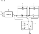
- FIG. 6 is a view illustrating a 23W-AC-driven LED lighting device for preventing a flicker according to the present disclosure.
- FIG. 7 is a circuit diagram illustrating the LED lighting device in FIG. 6 .
- the LED lighting device is provided with an AC power supply 10, a rectifying unit 20, first and second light-emitting units 100, 200, first and second diodes (D1 and D2) and a series-type switching unit 50.
- the first light-emitting unit 100 includes a first LED array (LA1), a first electrolytic capacitor (EC1), a first discharge resistance (RC1) and a first constant-current adjusting unit 150
- the second light-emitting unit 200 includes a second LED array (LA2), a second electrolytic capacitor (EC2), a second discharge resistance (RC2) and a second constant-current adjusting unit 250.
- the first constant-current adjusting unit 150 is provided with a first drain resistance (RT1D), a first gate resistance (RT1G), a first gate-voltage-maintenance capacitor (CT1G), a first current-control resistance (RT1S) and a first current-branch resistance (RTM1)
- the second constant-current adjusting unit 250 is provided with a second drain resistance (RT2D), a second gate resistance (RT2G), a second gate-voltage-maintenance capacitor (CT2G), a second current-control resistance (RT2S) and a second current-branch resistance (RTM2).
- the series-type switching unit 50 includes a power-supply resistance (R1), a Zener diode (Z1), gate-voltage-branch resistances (R2, R3 and R4), and first and second transistors (Q1 and Q2).
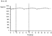
- FIG. 8 is a graph illustrating a flicker waveform measured in the LED lighting device in FIG. 7 .
- FIG. 9 compares the picture taken with the camera in the state in which the LED lighting device of FIG. 7 emits light compared to the prior art.
- each component of the LED lighting device for preventing a flicker according to the present disclosure is schematically described as follows with reference to FIGS. 6 to 9 .
- a rectifying unit 20 is supplied with an AC voltage from an AC power supply 10 and rectifies the same, to output a direct current.
- a first light-emitting unit 100 is supplied with the direct current from the rectifying unit 20 and adjusts a first constant current, to allow a first LED array (LA1) to emit light.
- a second light-emitting unit 200 is supplied with the adjusted first constant current from the first light-emitting unit 100 and adjusts a second constant current, to allow a second LED array (LA2) to emit light.
- LA2 second LED array
- a series-type switching unit 50 is supplied with the direct current from the rectifying unit 20 and the adjusted first and second constant currents respectively from the first and second light-emitting units 100, 200, and controls delivery of an electric current on the basis of opening and closing of a plurality of transistors (Q1 and Q2) built into the series-type switching unit.
- a current-amount-control resistance is commonly connected to a source terminal of first and second transistors (Q1 and Q2) and the other side is grounded, to control a current amount of the series-type switching unit 50.
- the direct current, supplied to the first light-emitting unit 100, is supplied by passing through a first diode (D1), and the first constant current, supplied to the second light-emitting unit 200, is supplied by passing through a second diode (D2).
- each component of the first light-emitting unit 100 in the LED lighting device for preventing a flicker according to the present disclosure are specifically described as follows with reference to FIGS. 6 to 9 .
- One side of a first electrolytic capacitor (EC1) is connected to a cathode terminal of a first diode (D1), and the other side is connected to an anode terminal of a second diode (D2), to charge first electric charge.
- a first discharge resistance (RC1) is connected in parallel with the first electrolytic capacitor (EC1) to discharge the charged first electric charge.
- the first LED array (LA1) is provided with a plurality of LEDs (not illustrated), and is supplied with a direct current to emit light.
- One side of a first constant-current adjusting unit 150 is connected to an output terminal of the first LED array (LA1), and the other side is connected to the anode terminal of the second diode (D2), to adjust and output the first constant current where a gate bias is adjusted.
- each component of the first constant-current adjusting unit 150 in the LED lighting device for preventing a flicker according to the present disclosure are specifically described as follows with reference to FIGS. 6 to 9 .
- One side of a first field-effect transistor (T1) is connected to an output terminal of a first LED array (LA1) to adjust a gate bias, and switches a flow of a first constant current.
- One side of a first drain resistance (RT1D) is connected to a drain terminal of the first field-effect transistor (T1), and the other side is connected to a gate terminal of the first field-effect transistor (T1), to adjust a gate bias.
- One side of a first current-branch resistance (RTM1) is connected to the drain terminal of the first field-effect transistor (T1), and the other side is connected to a source terminal of the first field-effect transistor (T1), to branch a drain current of the first field-effect transistor (T1).
- R1S first current-control resistance
- T1 One side of a first current-control resistance (RT1S) is connected to the source terminal of the first field-effect transistor (T1), and the other side is connected to the anode terminal of the second diode (D2), to control a source current of the first field-effect transistor (T1).
- R1S first current-control resistance
- R1G One side of a first gate resistance (RT1G) is connected to the gate terminal of the first field-effect transistor (T1), and the other side is connected to the anode terminal of the second diode (D2), to adjust a gate bias.
- a first gate-voltage-maintenance capacitor (CT1G) is connected in parallel with the first gate resistance (RT1G) to keep a first gate voltage constant with respect to a fluctuating first drain voltage of the first field-effect transistor (T1).
- each component of the second light-emitting unit 200 in the LED lighting device for preventing a flicker according to the present disclosure are specifically described as follows with reference to FIGS. 6 to 9 .
- One side of a second electrolytic capacitor (EC2) is connected to a cathode terminal of a second diode (D2) to charge second electric charge.
- a second discharge resistance (RC2) is connected in parallel with the second electrolytic capacitor (EC2) to discharge the charged second electric charge.
- a second LED array (LA2) is provided with a plurality of LEDs (not illustrated) and is supplied with a direct current to emit light.
- One side of a second constant-current adjusting unit 250 is connected to an output terminal of the second LED array (LA2) to adjust and output a second constant current where a gate bias is adjusted.
- each component of the second constant-current adjusting unit 250 in the LED lighting device for preventing a flicker according to the present disclosure are specifically described as follows with reference to FIGS. 6 to 9 .
- T2 One side of a second field-effect transistor (T2) is connected to an output terminal of a second LED array (LA2) to adjust a gate bias, and switches a flow of a second constant current.
- R2D second drain resistance
- T2D drain terminal of the second field-effect transistor
- T2D gate terminal of the second field-effect transistor
- One side of a second current-branch resistance (RTM2) is connected to the drain terminal of the second field-effect transistor (T2), and the other side is connected to a source terminal of the second field-effect transistor (T2), to branch a drain current of the second field-effect transistor (T2).
- R2S second current-control resistance
- T2S The second current-control resistance
- T2S One side of a second current-control resistance (RT2S) is connected to the source terminal of the second field-effect transistor (T2), and the other side is connected to a series-type switching unit 50, to control a source current of the second field-effect transistor (T2).
- R2G second gate resistance
- T2G gate terminal of the second field-effect transistor
- D2 second diode
- a second gate-voltage-maintenance capacitor (CT2G) is connected in parallel with the second gate resistance (RT2G) to keep a second gate voltage constant with respect to a fluctuating second drain voltage of the second field-effect transistor (T2).
- each component of the series-type switching unit 50 in the LED lighting device for preventing a flicker according to the present disclosure are specifically described as follows with reference to FIGS. 6 to 9 .
- One side of a power-supply resistance (R1) is connected to a rectifying unit 20, supplied with a direct current and supplied with a constant voltage.
- first to third branch resistances (R2, R3 and R4) is connected to the other side of the power-supply resistance (R1) to receive a constant voltage. Additionally, the first to third branch resistances (R2, R3 and R4) are connected in series with each other and the other sides are grounded, to branch the received constant voltage.
- An anode terminal is grounded to a Zener diode (Z1), and the Zener diode (Z1) is connected in parallel with the first to third branch resistances (R2, R3 and R4) to prevent an overvoltage.
- a gate terminal is connected to a contact point of the first and second branch resistances (R2 and R3), and a drain terminal is supplied with a first constant current to be switched.
- a gate terminal is connected to a contact point of the second and third branch resistances (R3 and R4), and a drain terminal is supplied with a second constant current to be switched.
- a speed of charge in a normal state is based on a time constant defined by multiplying a dynamic resistance of each LED array (LAj) by capacitance (C_ECj) of each electrolytic capacitor (ECj), like that of the related art.
- discharge is based on a value of a constant current, which is proportional to an average of drain voltages, of a constant current circuit including the field-effect transistor (Tj) disclosed in the present disclosure.
- V_Tj gate bias of the field-effect transistor (Tj)
- RjD drain resistance
- RjG gate resistance
- CjG gate-voltage-maintenance capacitor
- VG Tj and VT_Tj are respectively a gate voltage and a threshold voltage of the field-effect transistor (Tj).
- the gate voltage (VG_Tj) of the field-effect transistor (Tj) is a voltage that is branched by the drain voltage (VD_Tj) of the field-effect transistor (Tj) and is calculated on the basis of the following formula.
- VG _ Tj VD _ Tj ⁇ RG _ Tj / RG _ Tj + RD _ Tj ⁇ ⁇
- ⁇ which is a factor when ⁇ is turned into a constant by a gate-voltage-maintenance capacitor (CTjG) may be a value smaller than 1.
- ⁇ is 2/ ⁇ . In fact, however, ⁇ is about 0.64 that is a little different from 2/ ⁇ . In the case of a triangle-wave-linear function, in the fluctuation of a drain voltage, ⁇ is 1/2. In fact, however, ⁇ is about 0.5 that is a little different from 1/2.
- a fluctuation of electric currents flowing to the field-effect transistor (Tj) is adjusted such that a desired target value of a flicker index is acquired at a slightly high power voltage considering a constant voltage or a margin.
- a drain resistance (RTjD), a gate resistance (RTjG) and a source resistance (RTjS) of the field-effect transistor (Tj) are respectively or entirely adjusted to acquire a desired flicker index.
- a value of capacitance may be doubled and an internal voltage may be halved.
- a flicker index may be adjusted to 3 % that is one tenth of 30 % by adjusting a resistance (RTjD, RTjG and RTjS) of the transistor.
- the present disclosure provides an LED lighting device for preventing a flicker that reduces a current ripple produced from an AC power supply of the LED lighting device by adjusting a constant current in the light-emitting unit, thereby preventing a flicker without increasing the number and capacity of electrolytic capacitors.
- LED lighting may be widely adopted in applications in which comfortable and accurate recognition of movements is an important factor and applications which include movement, vibration or rotation of an object.
- an LED driving apparatus for preventing a flicker, a failure rate of the electrolytic capacitor and LED lighting-emitting unit is decreased, thereby ensuring improved performance of a product and easily satisfying the standard of ENERGY STAR that is a program for certifying performance of an LED lighting device.
Landscapes
- Circuit Arrangement For Electric Light Sources In General (AREA)
Claims (5)
- LED-Beleuchtungsvorrichtung zur Verhinderung von Flimmern, umfassend;eine Gleichrichtereinheit (20), die so konfiguriert ist, dass sie mit einer Wechselspannung von einer Wechselstromversorgung (10) versorgt wird, die so konfiguriert ist, dass sie diese gleichrichtet, und die so konfiguriert ist, dass sie einen Gleichstrom ausgibt;eine erste lichtemittierende Einheit (100), die mit einem Teil des Gleichstroms versorgt wird, die so konfiguriert ist, dass sie einen ersten konstanten Strom einstellt, und die so konfiguriert ist, dass sie einer ersten LED-Anordnung (LA1) ermöglicht, Licht zu emittieren;eine zweite lichtemittierende Einheit (200), die mit einem Teil des eingestellten ersten Konstantstroms versorgt wird, die so konfiguriert ist, dass sie einen zweiten Konstantstrom einstellt, und die so konfiguriert ist, dass sie einer zweiten LED-Anordnung (LA2) ermöglicht, Licht zu emittieren; undeine Reihenschalteinheit (50), die mit dem verbleibenden Teil des Gleichstroms, dem verbleibenden Teil des eingestellten ersten Konstantstroms und dem eingestellten zweiten Konstantstrom versorgt wird und so konfiguriert ist, dass sie die Abgabe des verbleibenden Teils des Gleichstroms, des verbleibenden Teils des eingestellten ersten Konstantstroms und des eingestellten zweiten Konstantstroms auf der Grundlage des Öffnens und Schließens einer Vielzahl von in der Reihenschalteinheit (50) eingebauten Transistoren steuert,wobei der der ersten lichtemittierenden Einheit (100) zugeführte Strom durch Durchlaufen einer ersten Diode (D1) der LED-Beleuchtungsvorrichtung zugeführt wird und der der zweiten lichtemittierenden Einheit (200) zugeführte Strom durch Durchlaufen einer zweiten Diode (D2) der LED-Beleuchtungsvorrichtung zugeführt wird,wobei die erste lichtemittierende Einheit (100) umfasst:einen ersten Elektrolytkondensator (EC1), dessen eine Seite mit einem Kathodenanschluss der ersten Diode (D1) und dessen andere Seite mit einem Anodenanschluss der zweiten Diode (D2) verbunden ist, um eine erste elektrische Ladung zu laden;einen ersten Entladewiderstand (RC1), der parallel zu dem ersten Elektrolytkondensator (EC1) geschaltet und so konfiguriert ist, dass er die geladene erste elektrische Ladung entlädt;wobei die erste LED-Anordnung (LA1) mit einer Vielzahl von LEDs versehen ist, die mit einem Teil des Stroms versorgt werden, der durch die erste Diode (D1) geflossen ist, und so konfiguriert sind, dass sie Licht emittieren; undeine erste Konstantstrom-Einstelleinheit (150), deren eine Seite mit einem Ausgangsanschluss des ersten LED-Arrays (LA1) und deren andere Seite mit dem Anodenanschluss der zweiten Diode (D2) verbunden ist, um den ersten Konstantstrom einzustellen und auszugeben,wobei die erste Konstantstrom-Einstelleinheit (150) umfasst:einen ersten Feldeffekttransistor (T1) mit einem Drain-Anschluss, der mit dem Ausgangsanschluss des ersten LED-Arrays (LA1) verbunden ist und so konfiguriert ist, dass er einen Fluss des ersten Konstantstroms schaltet;einen ersten Drain-Widerstand (RT1D), wobei eine Seite mit dem Drain-Anschluss des ersten Feldeffekttransistors (T1) und die andere Seite mit einem Gate-Anschluss des ersten Feldeffekttransistors (T1) verbunden ist, um eine Gate-Vorspannung einzustellen;einen ersten Stromverzweigungswiderstand (RTM1), dessen eine Seite mit dem Drain-Anschluss des ersten Feldeffekttransistors (T1) und dessen andere Seite mit einem Source-Anschluss des ersten Feldeffekttransistors (T1) verbunden ist, um einen Drain-Strom des ersten Feldeffekttransistors (T1) zu verzweigen;einen ersten Stromsteuerungswiderstand (RT1S), dessen eine Seite mit dem Source-Anschluss des ersten Feldeffekttransistors (T1) und dessen andere Seite mit dem Anodenanschluss der zweiten Diode (D2) verbunden ist, um einen Source-Strom des ersten Feldeffekttransistors (T1) zu steuern;einen ersten Gate-Widerstand (RT1G), dessen eine Seite mit dem Gate-Anschluss des ersten Feldeffekttransistors (T1) und dessen andere Seite mit dem Anodenanschluss der zweiten Diode (D2) verbunden ist, um die Gate-Vorspannung einzustellen; undeinen ersten Gate-Spannungserhaltungskondensator (CT1G), der parallel zu dem ersten Gate-Widerstand (RT1G) geschaltet und so konfiguriert ist, dass er eine erste Gate-Spannung in Bezug auf eine schwankende erste Drain-Spannung des ersten Feldeffekttransistors (T1) konstant hält, undwobei die zweite lichtemittierende Einheit (200) umfasst:einen zweiten Elektrolytkondensator (EC2), dessen eine Seite mit einem Kathodenanschluss der zweiten Diode (D2) verbunden ist, um eine zweite elektrische Ladung zu laden;einen zweiten Entladewiderstand (RC2), der parallel zu dem zweiten Elektrolytkondensator (EC2) geschaltet und so konfiguriert ist, dass er die geladene zweite elektrische Ladung entlädt;wobei die zweite LED-Anordnung (LA2) mit einer Vielzahl von LEDs versehen ist, die mit einem Teil des Stroms versorgt werden, der durch die zweite Diode (D2) geflossen ist, und so konfiguriert sind, dass sie Licht emittieren; undeine zweite Konstantstrom-Einstelleinheit (250), deren eine Seite mit einem Ausgangsanschluss des zweiten LED-Arrays (LA2) verbunden ist, um den zweiten Konstantstrom einzustellen und auszugeben,wobei die zweite Konstantstrom-Einstelleinheit (250) umfasst:einen zweiten Feldeffekttransistor (T2) mit einem Drain-Anschluss, der mit einem Ausgangsanschluss der zweiten LED-Anordnung (LA2) verbunden ist und so konfiguriert ist, dass er einen Fluss des zweiten Konstantstroms schaltet;einen zweiten Drain-Widerstand (RT2D), dessen eine Seite mit dem Drain-Anschluss des zweiten Feldeffekttransistors (T2) und dessen andere Seite mit einem Gate-Anschluss des zweiten Feldeffekttransistors (T2) verbunden ist, um eine Gate-Vorspannung einzustellen;einen zweiten Stromverzweigungswiderstand (RTM2), dessen eine Seite mit dem Drain-Anschluss des zweiten Feldeffekttransistors (T2) und dessen andere Seite mit einem Source-Anschluss des zweiten Feldeffekttransistors (T2) verbunden ist, um einen Drain-Strom des zweiten Feldeffekttransistors (T2) zu verzweigen;einen zweiten Stromsteuerungswiderstand (RT2S), dessen eine Seite mit dem Source-Anschluss des zweiten Feldeffekttransistors (T2) verbunden ist und dessen andere Seite mit der Serienschalteinheit (50) verbunden ist, um einen Source-Strom des zweiten Feldeffekttransistors (T2) zu steuern;einen zweiten Gate-Widerstand (RT2G), dessen eine Seite mit dem Gate-Anschluss des zweiten Feldeffekttransistors (T2) und dessen andere Seite mit der Serienschalteinheit (50) verbunden ist, um die Gate-Vorspannung einzustellen; undeinen zweiten Gate-Spannungshaltekondensator (CT2G), der parallel zu dem zweiten Gate-Widerstand (RT2G) geschaltet und so konfiguriert ist, dass er eine zweite Gate-Spannung in Bezug auf eine schwankende zweite Drain-Spannung des zweiten Feldeffekttransistors (T2) konstant hält.
- LED-Beleuchtungsvorrichtung zur Verhinderung eines Flackerns nach Anspruch 1, wobei die Serienschalteinheit (50) umfasst:einen Stromversorgungswiderstand (R1), dessen eine Seite mit der Gleichrichtereinheit (20) verbunden ist, die mit dem restlichen Teil des Gleichstroms versorgt wird und die mit einer konstanten Spannung versorgt wird;die Widerstände des ersten bis dritten Zweigs (R2, R3, R4), die in Reihe geschaltet sind und deren eine Seite mit der anderen Seite des Versorgungswiderstands (R1) verbunden ist, um die konstante Spannung zu erhalten, und deren andere Seite geerdet ist, um die konstante Spannung abzuzweigen;eine Zenerdiode (Z1), deren Anodenanschluss geerdet ist, die parallel zu den Widerständen des ersten bis dritten Zweigs (R2, R3, R4) geschaltet ist und die so konfiguriert ist, dass sie eine Überspannung verhindert;einen ersten Transistor (Q1), dessen Gate-Anschluss mit einem Kontaktpunkt des ersten und zweiten Zweigwiderstands (R2, R3) verbunden ist und dessen Drain-Anschluss mit dem verbleibenden Teil des ersten Konstantstroms versorgt wird; undeinen zweiten Transistor (Q2), dessen Gate-Anschluss mit einem Kontaktpunkt des zweiten und dritten Zweigwiderstands (R3, R4) verbunden ist und dessen Drain-Anschluss mit dem zweiten Konstantstrom versorgt wird,wobei die Source-Anschlüsse des ersten und zweiten Transistors (Q1, Q2) miteinander verbunden sind.
- LED-Beleuchtungsvorrichtung zur Verhinderung eines Flackerns nach Anspruch 2, wobei die Schalteinheit der Serie (50) weiterhin umfasst:
einen Strommengen-Steuerwiderstand (RS), dessen eine Seite gemeinsam mit den Source-Anschlüssen des ersten und des zweiten Transistors (Q1, Q2) verbunden ist und dessen andere Seite geerdet ist, der so konfiguriert ist, dass er eine durch die Transistoren (Q1, Q2) der Serien-Schalteinheit (50) geleitete Strommenge steuert. - LED-Beleuchtungsvorrichtung zur Verhinderung eines Flackerns nach Anspruch 1, wobei der erste Elektrolytkondensator (EC1) so konfiguriert ist, dass er
mit einer Geschwindigkeit geladen wird, die auf einer Zeitkonstante basiert, die durch definiert ist, dem Ergebnis einer Multiplikation von einem dynamischen Widerstand des ersten LED-Arrays (LA1) und einer Kapazität des ersten Elektrolytkondensators (EC1). - LED-Beleuchtungsvorrichtung zur Verhinderung eines Flackerns nach Anspruch 1, wobei der zweite Elektrolytkondensator (EC2) so konfiguriert ist, dass er
mit einer Geschwindigkeit geladen wird, die auf einer Zeitkonstante basiert, die durch das Ergebnis einer Multiplikation eines dynamischen Widerstands der zweiten LED-Anordnung und einer Kapazität des zweiten Elektrolytkondensators (EC2) definiert ist.
Applications Claiming Priority (2)
| Application Number | Priority Date | Filing Date | Title |
|---|---|---|---|
| KR1020170139928A KR102018365B1 (ko) | 2017-10-26 | 2017-10-26 | 플리커 방지용 led 조명 장치 |
| PCT/KR2018/005744 WO2019083110A1 (ko) | 2017-10-26 | 2018-05-18 | 플리커 방지용 led 조명 장치 |
Publications (3)
| Publication Number | Publication Date |
|---|---|
| EP3703468A1 EP3703468A1 (de) | 2020-09-02 |
| EP3703468A4 EP3703468A4 (de) | 2021-07-07 |
| EP3703468B1 true EP3703468B1 (de) | 2022-11-16 |
Family
ID=66246536
Family Applications (1)
| Application Number | Title | Priority Date | Filing Date |
|---|---|---|---|
| EP18871480.2A Active EP3703468B1 (de) | 2017-10-26 | 2018-05-18 | Led-beleuchtungsvorrichtung zur verhinderung von flackern |
Country Status (4)
| Country | Link |
|---|---|
| US (1) | US11076459B2 (de) |
| EP (1) | EP3703468B1 (de) |
| KR (1) | KR102018365B1 (de) |
| WO (1) | WO2019083110A1 (de) |
Families Citing this family (2)
| Publication number | Priority date | Publication date | Assignee | Title |
|---|---|---|---|---|
| EP4072248B1 (de) * | 2021-04-08 | 2024-08-07 | Controlled Oy | Flimmerreduktionsschaltung |
| KR102896600B1 (ko) | 2025-05-12 | 2025-12-08 | 주식회사 천일 | Ai 기반 플리커 저감 디밍 최적화 조명 제어시스템 |
Family Cites Families (8)
| Publication number | Priority date | Publication date | Assignee | Title |
|---|---|---|---|---|
| US8569956B2 (en) * | 2009-06-04 | 2013-10-29 | Point Somee Limited Liability Company | Apparatus, method and system for providing AC line power to lighting devices |
| KR101357636B1 (ko) | 2012-02-08 | 2014-02-04 | (주)로그인디지탈 | 플리커 제거 기능의 고효율 직결형 엘이디 구동 회로 |
| KR20140100394A (ko) * | 2013-02-05 | 2014-08-14 | 주식회사 루멘스 | 블럭으로 구성된 엘이디부를 포함하는 엘이디 조명장치 |
| DE102013107499A1 (de) * | 2013-07-15 | 2015-01-15 | RIVA GmbH Lighting | Vorrichtung und Verfahren zum direkten Betreiben einer Mehrzahl von Leuchtdioden an einer pulsierenden Gleichspannung |
| KR101635549B1 (ko) | 2014-03-18 | 2016-07-04 | 주식회사 르코어테크놀러지 | Led 구동 집적회로 및 그 구동 방법 |
| KR20160125241A (ko) * | 2015-04-21 | 2016-10-31 | 주식회사 아노덴 | 플리커 방지용 led 구동 장치 |
| KR101618544B1 (ko) | 2015-10-21 | 2016-05-10 | (주)유양디앤유 | 플리커리스 led 드라이버 장치 |
| KR101778494B1 (ko) * | 2017-06-08 | 2017-09-13 | 주식회사 에피룩스 | 플리커 제거 기능을 가지는 교류 및 직류 겸용 광원제어장치 |
-
2017
- 2017-10-26 KR KR1020170139928A patent/KR102018365B1/ko active Active
-
2018
- 2018-05-18 WO PCT/KR2018/005744 patent/WO2019083110A1/ko not_active Ceased
- 2018-05-18 EP EP18871480.2A patent/EP3703468B1/de active Active
- 2018-05-18 US US16/757,227 patent/US11076459B2/en active Active
Also Published As
| Publication number | Publication date |
|---|---|
| KR102018365B1 (ko) | 2019-09-04 |
| US20200281057A1 (en) | 2020-09-03 |
| EP3703468A1 (de) | 2020-09-02 |
| EP3703468A4 (de) | 2021-07-07 |
| KR20190046298A (ko) | 2019-05-07 |
| US11076459B2 (en) | 2021-07-27 |
| WO2019083110A1 (ko) | 2019-05-02 |
Similar Documents
| Publication | Publication Date | Title |
|---|---|---|
| CN102640306B (zh) | Led驱动电路 | |
| US8853954B2 (en) | Power supply for illumination and luminaire | |
| US8164276B2 (en) | LED drive device, LED drive method and lighting system | |
| KR101302182B1 (ko) | 발광다이오드의 점멸주파수를 변환시키는 전원공급회로 | |
| CN102186283A (zh) | 一种可控硅调光电路、调光方法以及应用其的一种led驱动电路 | |
| US8742696B2 (en) | Illuminating apparatus and method thereof | |
| CN110933816A (zh) | 适用于极低triac调光深度的led电流纹波消除电路 | |
| US20160014862A1 (en) | Control circuit of led lighting apparatus | |
| TW201325302A (zh) | 發光二極體驅動裝置及其方法 | |
| US20150327341A1 (en) | Control circuit of led lighting apparatus | |
| US8569961B2 (en) | Light emitting apparatus using AC LED | |
| US8749164B2 (en) | Illuminating apparatus capable of detecting power supply and method using the same | |
| US11076459B2 (en) | LED lighting device for preventing flickering | |
| US9743479B2 (en) | LED lighting apparatus with improved flicker index | |
| US20160037594A1 (en) | Lighting device, illuminating device and light fixture | |
| US9730287B2 (en) | Lighting apparatus and dimming regulation circuit thereof | |
| US20130099671A1 (en) | Power supply device and driving device | |
| TWI519204B (zh) | 具備多級驅動階段之發光二極體照明裝置 | |
| US10128654B2 (en) | Method and apparatus for correcting for power harmonics | |
| KR20160032370A (ko) | 교류 직결형 조명 장치의 구동 회로 및 방법 | |
| KR20150017442A (ko) | Led 조명기구 | |
| KR102297781B1 (ko) | 발광소자 구동회로 | |
| KR20130104143A (ko) | Led 전원 장치. | |
| US20150173150A1 (en) | Balanced AC Direct Driver Lighting System with a Valley Fill Circuit and a Light Balancer | |
| CN109699101B (zh) | 发光二极管照明装置 |
Legal Events
| Date | Code | Title | Description |
|---|---|---|---|
| STAA | Information on the status of an ep patent application or granted ep patent |
Free format text: STATUS: THE INTERNATIONAL PUBLICATION HAS BEEN MADE |
|
| PUAI | Public reference made under article 153(3) epc to a published international application that has entered the european phase |
Free format text: ORIGINAL CODE: 0009012 |
|
| STAA | Information on the status of an ep patent application or granted ep patent |
Free format text: STATUS: REQUEST FOR EXAMINATION WAS MADE |
|
| 17P | Request for examination filed |
Effective date: 20200424 |
|
| AK | Designated contracting states |
Kind code of ref document: A1 Designated state(s): AL AT BE BG CH CY CZ DE DK EE ES FI FR GB GR HR HU IE IS IT LI LT LU LV MC MK MT NL NO PL PT RO RS SE SI SK SM TR |
|
| AX | Request for extension of the european patent |
Extension state: BA ME |
|
| DAV | Request for validation of the european patent (deleted) | ||
| DAX | Request for extension of the european patent (deleted) | ||
| REG | Reference to a national code |
Ref country code: DE Ref legal event code: R079 Ref document number: 602018043239 Country of ref document: DE Free format text: PREVIOUS MAIN CLASS: H05B0033080000 Ipc: H05B0045480000 |
|
| A4 | Supplementary search report drawn up and despatched |
Effective date: 20210607 |
|
| RIC1 | Information provided on ipc code assigned before grant |
Ipc: H05B 45/48 20200101AFI20210531BHEP Ipc: H05B 45/345 20200101ALI20210531BHEP Ipc: H05B 45/395 20200101ALI20210531BHEP |
|
| GRAP | Despatch of communication of intention to grant a patent |
Free format text: ORIGINAL CODE: EPIDOSNIGR1 |
|
| STAA | Information on the status of an ep patent application or granted ep patent |
Free format text: STATUS: GRANT OF PATENT IS INTENDED |
|
| INTG | Intention to grant announced |
Effective date: 20220629 |
|
| GRAS | Grant fee paid |
Free format text: ORIGINAL CODE: EPIDOSNIGR3 |
|
| GRAA | (expected) grant |
Free format text: ORIGINAL CODE: 0009210 |
|
| STAA | Information on the status of an ep patent application or granted ep patent |
Free format text: STATUS: THE PATENT HAS BEEN GRANTED |
|
| RAP1 | Party data changed (applicant data changed or rights of an application transferred) |
Owner name: ISLT CO., LTD. |
|
| RIN1 | Information on inventor provided before grant (corrected) |
Inventor name: GONG, DA-YOUNG Inventor name: GONG, MYEONG-KOOK |
|
| AK | Designated contracting states |
Kind code of ref document: B1 Designated state(s): AL AT BE BG CH CY CZ DE DK EE ES FI FR GB GR HR HU IE IS IT LI LT LU LV MC MK MT NL NO PL PT RO RS SE SI SK SM TR |
|
| REG | Reference to a national code |
Ref country code: GB Ref legal event code: FG4D |
|
| REG | Reference to a national code |
Ref country code: CH Ref legal event code: EP |
|
| REG | Reference to a national code |
Ref country code: IE Ref legal event code: FG4D |
|
| REG | Reference to a national code |
Ref country code: DE Ref legal event code: R096 Ref document number: 602018043239 Country of ref document: DE |
|
| REG | Reference to a national code |
Ref country code: AT Ref legal event code: REF Ref document number: 1532550 Country of ref document: AT Kind code of ref document: T Effective date: 20221215 |
|
| REG | Reference to a national code |
Ref country code: LT Ref legal event code: MG9D |
|
| REG | Reference to a national code |
Ref country code: NL Ref legal event code: MP Effective date: 20221116 |
|
| REG | Reference to a national code |
Ref country code: AT Ref legal event code: MK05 Ref document number: 1532550 Country of ref document: AT Kind code of ref document: T Effective date: 20221116 |
|
| PG25 | Lapsed in a contracting state [announced via postgrant information from national office to epo] |
Ref country code: SE Free format text: LAPSE BECAUSE OF FAILURE TO SUBMIT A TRANSLATION OF THE DESCRIPTION OR TO PAY THE FEE WITHIN THE PRESCRIBED TIME-LIMIT Effective date: 20221116 Ref country code: PT Free format text: LAPSE BECAUSE OF FAILURE TO SUBMIT A TRANSLATION OF THE DESCRIPTION OR TO PAY THE FEE WITHIN THE PRESCRIBED TIME-LIMIT Effective date: 20230316 Ref country code: NO Free format text: LAPSE BECAUSE OF FAILURE TO SUBMIT A TRANSLATION OF THE DESCRIPTION OR TO PAY THE FEE WITHIN THE PRESCRIBED TIME-LIMIT Effective date: 20230216 Ref country code: LT Free format text: LAPSE BECAUSE OF FAILURE TO SUBMIT A TRANSLATION OF THE DESCRIPTION OR TO PAY THE FEE WITHIN THE PRESCRIBED TIME-LIMIT Effective date: 20221116 Ref country code: FI Free format text: LAPSE BECAUSE OF FAILURE TO SUBMIT A TRANSLATION OF THE DESCRIPTION OR TO PAY THE FEE WITHIN THE PRESCRIBED TIME-LIMIT Effective date: 20221116 Ref country code: ES Free format text: LAPSE BECAUSE OF FAILURE TO SUBMIT A TRANSLATION OF THE DESCRIPTION OR TO PAY THE FEE WITHIN THE PRESCRIBED TIME-LIMIT Effective date: 20221116 Ref country code: AT Free format text: LAPSE BECAUSE OF FAILURE TO SUBMIT A TRANSLATION OF THE DESCRIPTION OR TO PAY THE FEE WITHIN THE PRESCRIBED TIME-LIMIT Effective date: 20221116 |
|
| PG25 | Lapsed in a contracting state [announced via postgrant information from national office to epo] |
Ref country code: RS Free format text: LAPSE BECAUSE OF FAILURE TO SUBMIT A TRANSLATION OF THE DESCRIPTION OR TO PAY THE FEE WITHIN THE PRESCRIBED TIME-LIMIT Effective date: 20221116 Ref country code: PL Free format text: LAPSE BECAUSE OF FAILURE TO SUBMIT A TRANSLATION OF THE DESCRIPTION OR TO PAY THE FEE WITHIN THE PRESCRIBED TIME-LIMIT Effective date: 20221116 Ref country code: LV Free format text: LAPSE BECAUSE OF FAILURE TO SUBMIT A TRANSLATION OF THE DESCRIPTION OR TO PAY THE FEE WITHIN THE PRESCRIBED TIME-LIMIT Effective date: 20221116 Ref country code: IS Free format text: LAPSE BECAUSE OF FAILURE TO SUBMIT A TRANSLATION OF THE DESCRIPTION OR TO PAY THE FEE WITHIN THE PRESCRIBED TIME-LIMIT Effective date: 20230316 Ref country code: HR Free format text: LAPSE BECAUSE OF FAILURE TO SUBMIT A TRANSLATION OF THE DESCRIPTION OR TO PAY THE FEE WITHIN THE PRESCRIBED TIME-LIMIT Effective date: 20221116 Ref country code: GR Free format text: LAPSE BECAUSE OF FAILURE TO SUBMIT A TRANSLATION OF THE DESCRIPTION OR TO PAY THE FEE WITHIN THE PRESCRIBED TIME-LIMIT Effective date: 20230217 |
|
| PG25 | Lapsed in a contracting state [announced via postgrant information from national office to epo] |
Ref country code: NL Free format text: LAPSE BECAUSE OF FAILURE TO SUBMIT A TRANSLATION OF THE DESCRIPTION OR TO PAY THE FEE WITHIN THE PRESCRIBED TIME-LIMIT Effective date: 20221116 |
|
| P01 | Opt-out of the competence of the unified patent court (upc) registered |
Effective date: 20230526 |
|
| PG25 | Lapsed in a contracting state [announced via postgrant information from national office to epo] |
Ref country code: SM Free format text: LAPSE BECAUSE OF FAILURE TO SUBMIT A TRANSLATION OF THE DESCRIPTION OR TO PAY THE FEE WITHIN THE PRESCRIBED TIME-LIMIT Effective date: 20221116 Ref country code: RO Free format text: LAPSE BECAUSE OF FAILURE TO SUBMIT A TRANSLATION OF THE DESCRIPTION OR TO PAY THE FEE WITHIN THE PRESCRIBED TIME-LIMIT Effective date: 20221116 Ref country code: EE Free format text: LAPSE BECAUSE OF FAILURE TO SUBMIT A TRANSLATION OF THE DESCRIPTION OR TO PAY THE FEE WITHIN THE PRESCRIBED TIME-LIMIT Effective date: 20221116 Ref country code: DK Free format text: LAPSE BECAUSE OF FAILURE TO SUBMIT A TRANSLATION OF THE DESCRIPTION OR TO PAY THE FEE WITHIN THE PRESCRIBED TIME-LIMIT Effective date: 20221116 Ref country code: CZ Free format text: LAPSE BECAUSE OF FAILURE TO SUBMIT A TRANSLATION OF THE DESCRIPTION OR TO PAY THE FEE WITHIN THE PRESCRIBED TIME-LIMIT Effective date: 20221116 |
|
| REG | Reference to a national code |
Ref country code: DE Ref legal event code: R097 Ref document number: 602018043239 Country of ref document: DE |
|
| PG25 | Lapsed in a contracting state [announced via postgrant information from national office to epo] |
Ref country code: SK Free format text: LAPSE BECAUSE OF FAILURE TO SUBMIT A TRANSLATION OF THE DESCRIPTION OR TO PAY THE FEE WITHIN THE PRESCRIBED TIME-LIMIT Effective date: 20221116 Ref country code: AL Free format text: LAPSE BECAUSE OF FAILURE TO SUBMIT A TRANSLATION OF THE DESCRIPTION OR TO PAY THE FEE WITHIN THE PRESCRIBED TIME-LIMIT Effective date: 20221116 |
|
| PLBE | No opposition filed within time limit |
Free format text: ORIGINAL CODE: 0009261 |
|
| STAA | Information on the status of an ep patent application or granted ep patent |
Free format text: STATUS: NO OPPOSITION FILED WITHIN TIME LIMIT |
|
| 26N | No opposition filed |
Effective date: 20230817 |
|
| PG25 | Lapsed in a contracting state [announced via postgrant information from national office to epo] |
Ref country code: SI Free format text: LAPSE BECAUSE OF FAILURE TO SUBMIT A TRANSLATION OF THE DESCRIPTION OR TO PAY THE FEE WITHIN THE PRESCRIBED TIME-LIMIT Effective date: 20221116 |
|
| REG | Reference to a national code |
Ref country code: CH Ref legal event code: PL |
|
| PG25 | Lapsed in a contracting state [announced via postgrant information from national office to epo] |
Ref country code: MC Free format text: LAPSE BECAUSE OF FAILURE TO SUBMIT A TRANSLATION OF THE DESCRIPTION OR TO PAY THE FEE WITHIN THE PRESCRIBED TIME-LIMIT Effective date: 20221116 |
|
| REG | Reference to a national code |
Ref country code: BE Ref legal event code: MM Effective date: 20230531 |
|
| PG25 | Lapsed in a contracting state [announced via postgrant information from national office to epo] |
Ref country code: MC Free format text: LAPSE BECAUSE OF FAILURE TO SUBMIT A TRANSLATION OF THE DESCRIPTION OR TO PAY THE FEE WITHIN THE PRESCRIBED TIME-LIMIT Effective date: 20221116 Ref country code: LU Free format text: LAPSE BECAUSE OF NON-PAYMENT OF DUE FEES Effective date: 20230518 Ref country code: LI Free format text: LAPSE BECAUSE OF NON-PAYMENT OF DUE FEES Effective date: 20230531 Ref country code: CH Free format text: LAPSE BECAUSE OF NON-PAYMENT OF DUE FEES Effective date: 20230531 |
|
| REG | Reference to a national code |
Ref country code: IE Ref legal event code: MM4A |
|
| PG25 | Lapsed in a contracting state [announced via postgrant information from national office to epo] |
Ref country code: IE Free format text: LAPSE BECAUSE OF NON-PAYMENT OF DUE FEES Effective date: 20230518 |
|
| PG25 | Lapsed in a contracting state [announced via postgrant information from national office to epo] |
Ref country code: IE Free format text: LAPSE BECAUSE OF NON-PAYMENT OF DUE FEES Effective date: 20230518 |
|
| PG25 | Lapsed in a contracting state [announced via postgrant information from national office to epo] |
Ref country code: BE Free format text: LAPSE BECAUSE OF NON-PAYMENT OF DUE FEES Effective date: 20230531 |
|
| PG25 | Lapsed in a contracting state [announced via postgrant information from national office to epo] |
Ref country code: BG Free format text: LAPSE BECAUSE OF FAILURE TO SUBMIT A TRANSLATION OF THE DESCRIPTION OR TO PAY THE FEE WITHIN THE PRESCRIBED TIME-LIMIT Effective date: 20221116 |
|
| PG25 | Lapsed in a contracting state [announced via postgrant information from national office to epo] |
Ref country code: BG Free format text: LAPSE BECAUSE OF FAILURE TO SUBMIT A TRANSLATION OF THE DESCRIPTION OR TO PAY THE FEE WITHIN THE PRESCRIBED TIME-LIMIT Effective date: 20221116 |
|
| PG25 | Lapsed in a contracting state [announced via postgrant information from national office to epo] |
Ref country code: CY Free format text: LAPSE BECAUSE OF FAILURE TO SUBMIT A TRANSLATION OF THE DESCRIPTION OR TO PAY THE FEE WITHIN THE PRESCRIBED TIME-LIMIT; INVALID AB INITIO Effective date: 20180518 |
|
| PG25 | Lapsed in a contracting state [announced via postgrant information from national office to epo] |
Ref country code: HU Free format text: LAPSE BECAUSE OF FAILURE TO SUBMIT A TRANSLATION OF THE DESCRIPTION OR TO PAY THE FEE WITHIN THE PRESCRIBED TIME-LIMIT; INVALID AB INITIO Effective date: 20180518 |
|
| PGFP | Annual fee paid to national office [announced via postgrant information from national office to epo] |
Ref country code: DE Payment date: 20250721 Year of fee payment: 8 |
|
| PG25 | Lapsed in a contracting state [announced via postgrant information from national office to epo] |
Ref country code: TR Free format text: LAPSE BECAUSE OF FAILURE TO SUBMIT A TRANSLATION OF THE DESCRIPTION OR TO PAY THE FEE WITHIN THE PRESCRIBED TIME-LIMIT Effective date: 20221116 |
|
| PGFP | Annual fee paid to national office [announced via postgrant information from national office to epo] |
Ref country code: GB Payment date: 20260521 Year of fee payment: 9 |
|
| PGFP | Annual fee paid to national office [announced via postgrant information from national office to epo] |
Ref country code: IT Payment date: 20260529 Year of fee payment: 9 |
|
| PGFP | Annual fee paid to national office [announced via postgrant information from national office to epo] |
Ref country code: FR Payment date: 20260522 Year of fee payment: 9 |