EP3703045A1 - Scanning driver and driving method therefor - Google Patents
Scanning driver and driving method therefor Download PDFInfo
- Publication number
- EP3703045A1 EP3703045A1 EP17929606.6A EP17929606A EP3703045A1 EP 3703045 A1 EP3703045 A1 EP 3703045A1 EP 17929606 A EP17929606 A EP 17929606A EP 3703045 A1 EP3703045 A1 EP 3703045A1
- Authority
- EP
- European Patent Office
- Prior art keywords
- shift register
- scanning
- signal
- scan lines
- selection
- Prior art date
- Legal status (The legal status is an assumption and is not a legal conclusion. Google has not performed a legal analysis and makes no representation as to the accuracy of the status listed.)
- Withdrawn
Links
- 238000000034 method Methods 0.000 title claims abstract description 16
- 230000000750 progressive effect Effects 0.000 claims description 19
- 102100029361 Aromatase Human genes 0.000 abstract description 6
- 101000919395 Homo sapiens Aromatase Proteins 0.000 abstract description 6
- 101000869896 Homo sapiens Death-inducer obliterator 1 Proteins 0.000 abstract description 4
- 101001053773 Homo sapiens Type I iodothyronine deiodinase Proteins 0.000 abstract description 4
- 101001053754 Homo sapiens Type II iodothyronine deiodinase Proteins 0.000 abstract description 4
- 102100024063 Type I iodothyronine deiodinase Human genes 0.000 abstract description 4
- 102100024060 Type II iodothyronine deiodinase Human genes 0.000 abstract description 4
- 230000003321 amplification Effects 0.000 abstract 1
- 238000006243 chemical reaction Methods 0.000 abstract 1
- 238000003199 nucleic acid amplification method Methods 0.000 abstract 1
- 238000006467 substitution reaction Methods 0.000 description 2
Images


Classifications
-
- G—PHYSICS
- G09—EDUCATION; CRYPTOGRAPHY; DISPLAY; ADVERTISING; SEALS
- G09G—ARRANGEMENTS OR CIRCUITS FOR CONTROL OF INDICATING DEVICES USING STATIC MEANS TO PRESENT VARIABLE INFORMATION
- G09G3/00—Control arrangements or circuits, of interest only in connection with visual indicators other than cathode-ray tubes
- G09G3/20—Control arrangements or circuits, of interest only in connection with visual indicators other than cathode-ray tubes for presentation of an assembly of a number of characters, e.g. a page, by composing the assembly by combination of individual elements arranged in a matrix no fixed position being assigned to or needed to be assigned to the individual characters or partial characters
-
- G—PHYSICS
- G11—INFORMATION STORAGE
- G11C—STATIC STORES
- G11C19/00—Digital stores in which the information is moved stepwise, e.g. shift registers
- G11C19/28—Digital stores in which the information is moved stepwise, e.g. shift registers using semiconductor elements
-
- G—PHYSICS
- G11—INFORMATION STORAGE
- G11C—STATIC STORES
- G11C19/00—Digital stores in which the information is moved stepwise, e.g. shift registers
- G11C19/28—Digital stores in which the information is moved stepwise, e.g. shift registers using semiconductor elements
- G11C19/287—Organisation of a multiplicity of shift registers
-
- G—PHYSICS
- G09—EDUCATION; CRYPTOGRAPHY; DISPLAY; ADVERTISING; SEALS
- G09G—ARRANGEMENTS OR CIRCUITS FOR CONTROL OF INDICATING DEVICES USING STATIC MEANS TO PRESENT VARIABLE INFORMATION
- G09G2310/00—Command of the display device
- G09G2310/02—Addressing, scanning or driving the display screen or processing steps related thereto
- G09G2310/0202—Addressing of scan or signal lines
-
- G—PHYSICS
- G09—EDUCATION; CRYPTOGRAPHY; DISPLAY; ADVERTISING; SEALS
- G09G—ARRANGEMENTS OR CIRCUITS FOR CONTROL OF INDICATING DEVICES USING STATIC MEANS TO PRESENT VARIABLE INFORMATION
- G09G2310/00—Command of the display device
- G09G2310/02—Addressing, scanning or driving the display screen or processing steps related thereto
- G09G2310/0202—Addressing of scan or signal lines
- G09G2310/0213—Addressing of scan or signal lines controlling the sequence of the scanning lines with respect to the patterns to be displayed, e.g. to save power
-
- G—PHYSICS
- G09—EDUCATION; CRYPTOGRAPHY; DISPLAY; ADVERTISING; SEALS
- G09G—ARRANGEMENTS OR CIRCUITS FOR CONTROL OF INDICATING DEVICES USING STATIC MEANS TO PRESENT VARIABLE INFORMATION
- G09G2310/00—Command of the display device
- G09G2310/02—Addressing, scanning or driving the display screen or processing steps related thereto
- G09G2310/0202—Addressing of scan or signal lines
- G09G2310/0216—Interleaved control phases for different scan lines in the same sub-field, e.g. initialization, addressing and sustaining in plasma displays that are not simultaneous for all scan lines
-
- G—PHYSICS
- G09—EDUCATION; CRYPTOGRAPHY; DISPLAY; ADVERTISING; SEALS
- G09G—ARRANGEMENTS OR CIRCUITS FOR CONTROL OF INDICATING DEVICES USING STATIC MEANS TO PRESENT VARIABLE INFORMATION
- G09G2310/00—Command of the display device
- G09G2310/02—Addressing, scanning or driving the display screen or processing steps related thereto
- G09G2310/0243—Details of the generation of driving signals
-
- G—PHYSICS
- G09—EDUCATION; CRYPTOGRAPHY; DISPLAY; ADVERTISING; SEALS
- G09G—ARRANGEMENTS OR CIRCUITS FOR CONTROL OF INDICATING DEVICES USING STATIC MEANS TO PRESENT VARIABLE INFORMATION
- G09G2310/00—Command of the display device
- G09G2310/02—Addressing, scanning or driving the display screen or processing steps related thereto
- G09G2310/0264—Details of driving circuits
- G09G2310/0267—Details of drivers for scan electrodes, other than drivers for liquid crystal, plasma or OLED displays
-
- G—PHYSICS
- G09—EDUCATION; CRYPTOGRAPHY; DISPLAY; ADVERTISING; SEALS
- G09G—ARRANGEMENTS OR CIRCUITS FOR CONTROL OF INDICATING DEVICES USING STATIC MEANS TO PRESENT VARIABLE INFORMATION
- G09G2310/00—Command of the display device
- G09G2310/02—Addressing, scanning or driving the display screen or processing steps related thereto
- G09G2310/0264—Details of driving circuits
- G09G2310/0286—Details of a shift registers arranged for use in a driving circuit
-
- G—PHYSICS
- G09—EDUCATION; CRYPTOGRAPHY; DISPLAY; ADVERTISING; SEALS
- G09G—ARRANGEMENTS OR CIRCUITS FOR CONTROL OF INDICATING DEVICES USING STATIC MEANS TO PRESENT VARIABLE INFORMATION
- G09G2310/00—Command of the display device
- G09G2310/06—Details of flat display driving waveforms
- G09G2310/067—Special waveforms for scanning, where no circuit details of the gate driver are given
-
- G—PHYSICS
- G09—EDUCATION; CRYPTOGRAPHY; DISPLAY; ADVERTISING; SEALS
- G09G—ARRANGEMENTS OR CIRCUITS FOR CONTROL OF INDICATING DEVICES USING STATIC MEANS TO PRESENT VARIABLE INFORMATION
- G09G2310/00—Command of the display device
- G09G2310/08—Details of timing specific for flat panels, other than clock recovery
Definitions
- the disclosure relates to a display technical field, and more particularly to a scan driver and a driving method of the scan driver.
- the existing scan driver (shown as FIG. 1 ) only could driving the type for progressive scanning (shown as FIG. 2 and FIG. 3 ) base on the shift register. In some circuit which has special function requirement, it needs to scan the scan line by non-sequential scanning, and the existing scan driver cannot to satisfy that.
- a technical problem to be solved by the disclosure is to provide a scan driver and a driving method of the scan driver with satisfy requirement of progressive scanning and non-sequential scanning.
- the disclosure further provides a scan driver, comprising a first shift register receiving a first clock signal and a first initial pulse signal from a controller according to a first scanning type scans scan lines; a second shift register receiving a second clock signal and a second initial pulse signal from the controller according to a second scanning type scans scan lines; a selection unit connecting the first shift register and the second shift register, which receiving selection signals from the controller to select the first shift register for scanning scan lines by the first scanning type or the second shift register for scanning scan lines by the second scanning type; a logic control unit connecting the selection unit, which receiving an output enable signal from the controller and controls the outputting from an outputting terminal of a scanning driver according to the output enable signal; a level shift unit connecting the logic control unit, which outputting a level signal; and an output amplifier connecting the level shift unit, which amplifying the level signal and outputting an amplifying level signal from the outputting terminal of the scanning driver to the scan lines; wherein frequency of the first shift register is less than frequency of the second shift register, and the first shift register
- the disclosure further provides a scan driver, comprising:
- the disclosure further provides a driving method of scan driver, comprising:
- the scan driver and driving method of scan driver of this present invention is that using the first shift register to achieve progressive scanning and using the second shift register to achieve non-sequential scanning, and the selection unit receiving selection signals from the controller and select to work the first shift register or the second shift register. And then the logic control unit controls to outputting of the output terminal of scan driver. It achieves to satisfy requirement of progressive scanning and non-sequential scanning of scan driver.
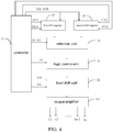
- FIG. 4 is a structural schematic view of a scan driver according to an embodiment of the disclosure.
- the scan driver comprising a first shift register 10 receiving a first clock signal CPV1 and a first initial pulse signal DIO1 from a controller 70 according to a first scanning type scans scan lines.
- the second shift register 20 receiving a second clock signal CPV2 and a second initial pulse signal DIO2 from the controller 70 according to a second scanning type scans scan lines.
- the selection unit 30 is connecting the first shift register 10 and the second shift register 20, which receiving selection signals SR_SEL from the controller 70 to select the first shift register 10 for scanning scan lines by the first scanning type or the second shift register 20 for scanning scan lines by the second scanning type.
- the logic control unit 40 is connecting the selection unit 30, which receiving an output enable signal OE from controller 70 and controls the outputting from an outputting terminal of a scanning driver according to the output enable signal OE.
- the level shift unit 50 is connecting the logic control unit 40, which outputting a level signal.
- the output amplifier 60 is connecting the level shift unit 50, which amplifying the level signal and outputting an amplifying level signal (the level signal is 1 or 0) from the outputting terminal Gn of the scanning driver to the scan lines.
- frequency of the first shift register 10 is less than frequency of the second shift register 20, and the first shift register 10 scans a valid region by progressive scanning, the second shift register 20 scans invalid region by non-sequential scanning.
- the selection signals SR_SEL received by the selection unit 30 from the controller 70 include a first selection signal and a second selection signal, the selection unit 30 selects the first shift register 10 for scanning scan lines by the first scanning type according to receive the first selection signal, the selection unit 30 selects the second shift register 20 for scanning scan lines by the second scanning type according to receive the second selection signal.
- the first shift register 10 and the second shift register 20 further receiving a gated clock signal CLK_GATE from the controller 70, and elongating enabling time of the scan lines by the gate clock signal CLK_GATE.
- the maximum operating frequency of existing scan driving will not be over 350KHZ, and because this frequency already satisfy existing using requirement.
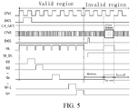
- FIG. 5 is a schematic view of a signal timing of scan driver of this present invention. As shown in FIG. 4 and FIG. 5 , the working principle of the first shift register 10 for scanning scan lines by the first scanning type (which is progressive scanning) described below.
- Address stage rapid scans to correspondingly scan line.
- the entire scan lines in turn-off status the output enable signal OE received from the logic control unit 40 from controller 70 is low potential level.
- the scan driver does not outputting, the first shift register 10 receiving the first clock signal CPV1 and the first initial pulse signal DIO1, and then the first shift register 10 working and the first shift register 10 scans a first scan line (forward scan, which is from first scan line progressive scan to last scan line, here will illustrate by forward scan) or last scan line (backward scan, which is from last scan line progressive scan to first scan line).
- Turn-on stage turn-on the correspondingly scan line, and turn-on the scan line for a certain time.
- the scan driver scans the correspondingly scan line (for example the first scan line)
- the output enable signal OE received by the logic control unit 40 from controller 70 is high potential level.
- the scan driver outputs a scan driver signal for controlling to turn-on the correspondingly scan line (for example the first scan line). Because a clock cycle is short, it cannot satisfy needs of turn-on time, such that the controller 70 outputs a gated clock signal CLK_GATE has low potential level to the first shift register 10, and made the first clock signal CPV1 failure. It could achieve to turn-on a certain time to the correspondingly scan line.
- Turn-off stage turn-off the correspondingly scan line which already turn-on, and finish to scan other scan lines.
- the controller 70 outputs a gated clock signal CLK_GATE has high potential level to the first shift register 10, enables the first clock signal CPV1.
- the scan driver will keep forward scan to other scan lines (for example a second scan line).
- turn-off the correspondingly scan line which already turn-on the scan principle for other scan lines as same as the described above, here is not repeat again. According the scan process above could achieve to progressive turn-on the scan line and holding a certain time, and it could achieve to progressive scanning.
- Address stage rapidly scans to scan line which needs to turn-on.
- the entire scan lines in turn-off status the output enable signal OE received from the logic control unit 40 from controller 70 is low potential level.
- the scan driver does not output, the second shift register 20 receiving the second clock signal CPV2 and the second initial pulse signal DIO2, then working to more highly frequency, and made the second shift register 20 rapidly scans to scan line which needs to turn-on.
- Turn-on stage turn-on the scan line which needs to turn-on, and holding the turn-on scan line for a certain time.
- the output enable signal OE received by the logic control unit 40 from controller 70 is high potential level.
- the scan driver outputs a scan driver signal for controlling to turn-on the scan line which needs to turn-on. Because a clock cycle is short, it cannot satisfy the needs turn-on time, such that the controller 70 outputs a gated clock signal CLK_GATE has low potential level to the second shift register 20, and made the second clock signal CPV2 failure. It could achieve to turn-on a certain time to the scan line which needs to turn-on.
- Turn-off stage turn-off the scan line which need to turn-on, and finishing to scan other scan lines which needs to turn-on.
- the controller 70 outputs a gated clock signal CLK_GATE has high potential level to the second shift register 20, enables the second clock signal CPV2.
- the scan driver will keep to forward scan other scan lines which need to turn-on.
- turn-off the scan line which needs turn-on the scan principle for other scan lines as same as the described above, here is not repeat again. According the scan process above could achieve to progressive turn-on the scan line which needs turn-on and holding a certain time, and it could achieve to progressive scanning.
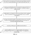
- FIG. 6 is a flowchart schematic view of a driving method of scan driver according to an embodiment of the disclosure.
- the step S1 includes: scanning a valid region by the first shift register 10 for progressive scanning;
- the step S2 includes: scanning a invalid region by the second shift register 20 for non-sequential scanning.
- the step S3 includes: the selection signals include a first selection signal and a second selection signal, the selection unit 30 selects the first shift register 10 for scanning scan lines by the first scanning type according to receive the first selection signal, the selection unit 30 selects the second shift register 20 for scanning scan lines by the second scanning type according to receive the second selection signal.
- the scan driver and driving method of scan driver is that using the first shift register to achieve progressive scanning and using the second shift register to achieve non-sequential scanning, and the selection unit revived selection signal from the controller and select working the first shift register or the second shift register. And then the logic control unit controls to outputting of the output terminal of scan driver. It achieves to satisfy requirement of progressive scanning and non-sequential scanning of scan driver.
Landscapes
- Engineering & Computer Science (AREA)
- Physics & Mathematics (AREA)
- Computer Hardware Design (AREA)
- General Physics & Mathematics (AREA)
- Theoretical Computer Science (AREA)
- Control Of Indicators Other Than Cathode Ray Tubes (AREA)
- Liquid Crystal Display Device Control (AREA)
Abstract
Description
- The present application is a National Phase of International Application Number
PCT/CN2017/112620, filed November 23, 2017 201711017742.5 filed October 25, 2017 - The disclosure relates to a display technical field, and more particularly to a scan driver and a driving method of the scan driver.
- The existing scan driver (shown as
FIG. 1 ) only could driving the type for progressive scanning (shown asFIG. 2 and FIG. 3 ) base on the shift register. In some circuit which has special function requirement, it needs to scan the scan line by non-sequential scanning, and the existing scan driver cannot to satisfy that. - A technical problem to be solved by the disclosure is to provide a scan driver and a driving method of the scan driver with satisfy requirement of progressive scanning and non-sequential scanning.
- Furthermore, the disclosure further provides a scan driver, comprising
a first shift register receiving a first clock signal and a first initial pulse signal from a controller according to a first scanning type scans scan lines;
a second shift register receiving a second clock signal and a second initial pulse signal from the controller according to a second scanning type scans scan lines;
a selection unit connecting the first shift register and the second shift register, which receiving selection signals from the controller to select the first shift register for scanning scan lines by the first scanning type or the second shift register for scanning scan lines by the second scanning type;
a logic control unit connecting the selection unit, which receiving an output enable signal from the controller and controls the outputting from an outputting terminal of a scanning driver according to the output enable signal;
a level shift unit connecting the logic control unit, which outputting a level signal; and
an output amplifier connecting the level shift unit, which amplifying the level signal and outputting an amplifying level signal from the outputting terminal of the scanning driver to the scan lines;
wherein frequency of the first shift register is less than frequency of the second shift register, and the first shift register scans a valid region by progressive scanning, the second shift register scans invalid region by non-sequential scanning;
wherein the selection signals received by the selection unit from the controller include a first selection signal and a second selection signal, the selection unit selects the first shift register for scanning scan lines by the first scanning type according to receive the first selection signal, the selection unit selects the second shift register for scanning scan lines by the second scanning type according to receive the second selection signal. - According to another aspect of the disclosure, the disclosure further provides a scan driver, comprising:
- a first shift register receiving a first clock signal and a first initial pulse signal from a controller according to a first scanning type scans scan lines;
- a second shift register receiving a second clock signal and a second initial pulse signal from the controller according to a second scanning type scans scan lines;
- a selection unit connecting the first shift register and the second shift register, which receiving selection signals from the controller to select the first shift register for scanning scan lines by the first scanning type or the second shift register for scanning scan lines by the second scanning type;
- a logic control unit connecting the selection unit, which receiving an output enable signal from controller and controls the outputting from an outputting terminal of a scanning driver according to the output enable signal;
- a level shift unit connecting the logic control unit, which outputting a level signal; and
- an output amplifier connecting the level shift unit, which amplifying the level signal and outputting an amplifying level signal from the outputting terminal of the scanning driver to the scan lines.
- According to another aspect of the disclosure, the disclosure further provides a driving method of scan driver, comprising:
- receiving a first clock signal and a first initial pulse signal from a controller by a first shift register according to a first scanning type scans scan lines;
- receiving a second clock signal and a second initial pulse signal from the controller by a second shift register according to a second scanning type scans scan lines;
- receiving selection signals from the controller to selection unit for selecting the first shift register for scanning scan lines by the first scanning type or the second shift register for scanning scan lines by the second scanning type;
- receiving an output enable signal from controller to a logic control unit and controls the outputting from an outputting terminal of a scanning driver according to the output enable signal;
- outputting a level signal outputted by the level shift unit; and
- amplifying the level signal by an output amplifier and outputting an amplifying level signal from the outputting terminal of the scanning driver to the scan lines.
- In sum: comparing with the existing technology, the scan driver and driving method of scan driver of this present invention is that using the first shift register to achieve progressive scanning and using the second shift register to achieve non-sequential scanning, and the selection unit receiving selection signals from the controller and select to work the first shift register or the second shift register. And then the logic control unit controls to outputting of the output terminal of scan driver. It achieves to satisfy requirement of progressive scanning and non-sequential scanning of scan driver.
- Accompanying drawings are for providing further understanding of embodiments of the disclosure. The drawings form a part of the disclosure and are for illustrating the principle of the embodiments of the disclosure along with the literal description. Apparently, the drawings in the description below are merely some embodiments of the disclosure, a person skilled in the art can obtain other drawings according to these drawings without creative efforts. In the figures:
-
FIG. 1 is a prior art structural schematic view of a scan driver; -
FIG. 2 is a schematic view of a signal timing ofFIG. 1 ; -
FIG. 3 is a prior art schematic view of an output waveform; -
FIG. 4 is a structural schematic view of a scan driver according to an embodiment of the disclosure; -
FIG. 5 is a schematic view of a signal timing ofFIG. 4 ; and -
FIG. 6 is a flowchart schematic view of a driving method of scan driver according to an embodiment of the disclosure. - The specific structural and functional details disclosed herein are only representative and are intended for describing exemplary embodiments of the disclosure. However, the disclosure can be embodied in many forms of substitution, and should not be interpreted as merely limited to the embodiments described herein.
- The disclosure will be further described in detail with reference to accompanying drawings and preferred embodiments as follows.
- Please refer to
FIG. 4. FIG. 4 is a structural schematic view of a scan driver according to an embodiment of the disclosure. The scan driver comprising afirst shift register 10 receiving a first clock signal CPV1 and a first initial pulse signal DIO1 from acontroller 70 according to a first scanning type scans scan lines. - The second shift register 20 receiving a second clock signal CPV2 and a second initial pulse signal DIO2 from the
controller 70 according to a second scanning type scans scan lines. - The
selection unit 30 is connecting thefirst shift register 10 and thesecond shift register 20, which receiving selection signals SR_SEL from thecontroller 70 to select thefirst shift register 10 for scanning scan lines by the first scanning type or thesecond shift register 20 for scanning scan lines by the second scanning type. - The
logic control unit 40 is connecting theselection unit 30, which receiving an output enable signal OE fromcontroller 70 and controls the outputting from an outputting terminal of a scanning driver according to the output enable signal OE. - The
level shift unit 50 is connecting thelogic control unit 40, which outputting a level signal. - The
output amplifier 60 is connecting thelevel shift unit 50, which amplifying the level signal and outputting an amplifying level signal (the level signal is 1 or 0) from the outputting terminal Gn of the scanning driver to the scan lines. - In this embodiment, frequency of the
first shift register 10 is less than frequency of thesecond shift register 20, and the first shift register 10 scans a valid region by progressive scanning, the second shift register 20 scans invalid region by non-sequential scanning. - Specifically, the selection signals SR_SEL received by the
selection unit 30 from thecontroller 70 include a first selection signal and a second selection signal, theselection unit 30 selects thefirst shift register 10 for scanning scan lines by the first scanning type according to receive the first selection signal, theselection unit 30 selects thesecond shift register 20 for scanning scan lines by the second scanning type according to receive the second selection signal. - In this embodiment, the
first shift register 10 and thesecond shift register 20 further receiving a gated clock signal CLK_GATE from thecontroller 70, and elongating enabling time of the scan lines by the gate clock signal CLK_GATE. - In this embodiment, the frequency the second clock signal CPV2 received by the
second shift register 20 is according to formula fCPV2>=(N-1)/(tVB-tOPEN), wherein fCPV2 is frequency of the second clock signal, N is number of scan lines, tVB is time of invalid time, tOPEN is enabling time of scan lines.. - The maximum operating frequency of existing scan driving will not be over 350KHZ, and because this frequency already satisfy existing using requirement. For example 4K2K UD @120Hz, the frequency of scan driver is fCPV=2160*120=259.2KHz, which could satisfy existing using requirement. Because the clock signal CPV directly applicants to the shift register, the frequency is effected by inner circuit of scan driver but not the shift register, so that the shift register could working on higher frequency.
- Please refer to
FIG. 5. FIG. 5 is a schematic view of a signal timing of scan driver of this present invention. As shown inFIG. 4 andFIG. 5 , the working principle of thefirst shift register 10 for scanning scan lines by the first scanning type (which is progressive scanning) described below. - Address stage: rapid scans to correspondingly scan line. In order to not affect display of panel, the entire scan lines in turn-off status, the output enable signal OE received from the
logic control unit 40 fromcontroller 70 is low potential level. At this time, the scan driver does not outputting, thefirst shift register 10 receiving the first clock signal CPV1 and the first initial pulse signal DIO1, and then thefirst shift register 10 working and thefirst shift register 10 scans a first scan line (forward scan, which is from first scan line progressive scan to last scan line, here will illustrate by forward scan) or last scan line (backward scan, which is from last scan line progressive scan to first scan line). - Turn-on stage: turn-on the correspondingly scan line, and turn-on the scan line for a certain time. When the scan driver scans the correspondingly scan line (for example the first scan line), the output enable signal OE received by the
logic control unit 40 fromcontroller 70 is high potential level. At this time, the scan driver outputs a scan driver signal for controlling to turn-on the correspondingly scan line (for example the first scan line). Because a clock cycle is short, it cannot satisfy needs of turn-on time, such that thecontroller 70 outputs a gated clock signal CLK_GATE has low potential level to thefirst shift register 10, and made the first clock signal CPV1 failure. It could achieve to turn-on a certain time to the correspondingly scan line. - Turn-off stage: turn-off the correspondingly scan line which already turn-on, and finish to scan other scan lines. When the corresponding scan line already turn-on for the certain time, the
controller 70 outputs a gated clock signal CLK_GATE has high potential level to thefirst shift register 10, enables the first clock signal CPV1. The scan driver will keep forward scan to other scan lines (for example a second scan line). When turn-off the correspondingly scan line which already turn-on, the scan principle for other scan lines as same as the described above, here is not repeat again. According the scan process above could achieve to progressive turn-on the scan line and holding a certain time, and it could achieve to progressive scanning. - The working principle of the
second shift register 20 for scanning scan lines by the second scanning type (which is non-sequential scanning) described below. - Address stage: rapidly scans to scan line which needs to turn-on. In order to not affect display of panel, the entire scan lines in turn-off status, the output enable signal OE received from the
logic control unit 40 fromcontroller 70 is low potential level. At this time, the scan driver does not output, thesecond shift register 20 receiving the second clock signal CPV2 and the second initial pulse signal DIO2, then working to more highly frequency, and made thesecond shift register 20 rapidly scans to scan line which needs to turn-on. - Turn-on stage: turn-on the scan line which needs to turn-on, and holding the turn-on scan line for a certain time. When the scan driver scans the scan line which need to turn-on, the output enable signal OE received by the
logic control unit 40 fromcontroller 70 is high potential level. At this time, the scan driver outputs a scan driver signal for controlling to turn-on the scan line which needs to turn-on. Because a clock cycle is short, it cannot satisfy the needs turn-on time, such that thecontroller 70 outputs a gated clock signal CLK_GATE has low potential level to thesecond shift register 20, and made the second clock signal CPV2 failure. It could achieve to turn-on a certain time to the scan line which needs to turn-on. - Turn-off stage: turn-off the scan line which need to turn-on, and finishing to scan other scan lines which needs to turn-on. When the scan line which needs turn-on already turn-on for the certain time, the
controller 70 outputs a gated clock signal CLK_GATE has high potential level to thesecond shift register 20, enables the second clock signal CPV2. The scan driver will keep to forward scan other scan lines which need to turn-on. When turn-off the scan line which needs turn-on, the scan principle for other scan lines as same as the described above, here is not repeat again. According the scan process above could achieve to progressive turn-on the scan line which needs turn-on and holding a certain time, and it could achieve to progressive scanning. - Please refer to
FIG. 6. FIG. 6 is a flowchart schematic view of a driving method of scan driver according to an embodiment of the disclosure. - Step S1, receiving a first clock signal CPV1 and a first initial pulse signal DIO1 from a
controller 70 by afirst shift register 10 according to a first scanning type scans scan lines; - Step S2, receiving a second clock signal CPV2 and a second initial pulse signal DIO2 from the
controller 70 by asecond shift register 20 according to a second scanning type scans scan lines; - Step S3, receiving selection signals from the
controller 70 to aselection unit 30 for selecting thefirst shift register 10 for scanning scan lines by the first scanning type or thesecond shift register 20 for scanning scan lines by the second scanning type; - Step S4, receiving an output enable signal OE from
controller 70 to alogic control unit 40 and controls the outputting from an outputting terminal Gn of a scanning driver according to the output enable signal OE; - Step S5, outputting a level signal outputted by the
level shift unit 50; and - Step S6, amplifying the level signal by an
output amplifier 60 and outputting an amplifying level signal from the outputting terminal Gn of the scanning driver to the scan lines. - Wherein, the step S1 includes:
scanning a valid region by thefirst shift register 10 for progressive scanning; - Wherein, the step S2 includes:
scanning a invalid region by thesecond shift register 20 for non-sequential scanning. - Wherein, the step S3 includes:
the selection signals include a first selection signal and a second selection signal, theselection unit 30 selects thefirst shift register 10 for scanning scan lines by the first scanning type according to receive the first selection signal, theselection unit 30 selects thesecond shift register 20 for scanning scan lines by the second scanning type according to receive the second selection signal. - The scan driver and driving method of scan driver is that using the first shift register to achieve progressive scanning and using the second shift register to achieve non-sequential scanning, and the selection unit revived selection signal from the controller and select working the first shift register or the second shift register. And then the logic control unit controls to outputting of the output terminal of scan driver. It achieves to satisfy requirement of progressive scanning and non-sequential scanning of scan driver.
- The foregoing contents are detailed description of the disclosure in conjunction with specific preferred embodiments and concrete embodiments of the disclosure are not limited to these description. For the person skilled in the art of the disclosure, without departing from the concept of the disclosure, simple deductions or substitutions can be made and should be included in the protection scope of the application.
Claims (11)
- A scan driver, comprising
a first shift register receiving a first clock signal and a first initial pulse signal from a controller according to a first scanning type scans scan lines; a second shift register receiving a second clock signal and a second initial pulse signal from the controller according to a second scanning type scans scan lines;
a selection unit connecting the first shift register and the second shift register, which receiving selection signals from the controller to select the first shift register for scanning scan lines by the first scanning type or the second shift register for scanning scan lines by the second scanning type; a logic control unit connecting the selection unit, which receiving an output enable signal from the controller and controls the outputting from an outputting terminal of a scanning driver according to the output enable signal;
a level shift unit connecting the logic control unit, which outputting a level signal; and
an output amplifier connecting the level shift unit, which amplifying the level signal and outputting an amplifying level signal from the outputting terminal of the scanning driver to the scan lines;
wherein frequency of the first shift register is less than frequency of the second shift register, and the first shift register scans a valid region by progressive scanning, the second shift register scans invalid region by non-sequential scanning;
wherein the selection signals received by the selection unit from the controller include a first selection signal and a second selection signal, the selection unit selects the first shift register for scanning scan lines by the first scanning type according to receive the first selection signal, the selection unit selects the second shift register for scanning scan lines by the second scanning type according to receive the second selection signal. - A scan driver, comprising:a first shift register receiving a first clock signal and a first initial pulse signal from a controller according to a first scanning type scans scan lines;a second shift register receiving a second clock signal and a second initial pulse signal from the controller according to a second scanning type scans scan lines;a selection unit connecting the first shift register and the second shift register, which receiving selection signals from the controller to select the first shift register for scanning scan lines by the first scanning type or the second shift register for scanning scan lines by the second scanning type;a logic control unit connecting the selection unit, which receiving an output enable signal from the controller and controls the outputting from an outputting terminal of a scanning driver according to the output enable signal;a level shift unit connecting the logic control unit, which outputting a level signal; andan output amplifier connecting the level shift unit, which amplifying the level signal and outputting an amplifying level signal from the outputting terminal of the scanning driver to the scan lines.
- The scan driver according to claim 2, wherein frequency of the first shift register is less than frequency of the second shift register, and the first shift register scans a valid region by progressive scanning, the second shift register scans invalid region by non-sequential scanning.
- The scan driver according to claim 2, wherein the selection signals received by the selection unit from the controller include a first selection signal and a second selection signal, the selection unit selects the first shift register for scanning scan lines by the first scanning type according to receive the first selection signal, the selection unit selects the second shift register for scanning scan lines by the second scanning type according to receive the second selection signal.
- The scan driver according to claim 2, wherein the first shift register and the second shift register further receiving a gated clock signal from the controller, and elongating enabling time of the scan lines by the gated clock signal.
- The scan driver according to claim 2, wherein frequency the second clock signal received by the second shift register is according to formula fCPV2>=(N-1)/(tVB-tOPEN), wherein fCPV2 is frequency of the second clock signal, N is number of scan lines, tVB is time of invalid time, tOPEN is enabling time of scan lines.
- A driving method of scan driver, comprising:receiving a first clock signal and a first initial pulse signal from a controller by a first shift register according to a first scanning type scans scan lines;receiving a second clock signal and a second initial pulse signal from the controller by a second shift register according to a second scanning type scans scan lines;receiving selection signals from the controller to a selection unit for selecting the first shift register for scanning scan lines by the first scanning type or the second shift register for scanning scan lines by the second scanning type;receiving an output enable signal from the controller to a logic control unit and controls the outputting from an outputting terminal of a scanning driver according to the output enable signal;outputting a level signal outputted by the level shift unit; andamplifying the level signal by an output amplifier and outputting an amplifying level signal from the outputting terminal of the scanning driver to the scan lines.
- The driving method of scan driver according to claim 7, wherein the step of receiving the first clock signal and a first initial pulse signal from the controller by the first shift register according to the first scanning type scans scan lines, comprising:scanning a valid region by the first shift register for progressive scanning;wherein the step of receiving the second clock signal and the second initial pulse signal from the controller by the second shift register according to the second scanning type scans scan lines, comprising:
scanning an invalid region by the second shift register for non-sequential scanning. - The driving method of scan driver according to claim 7, wherein the step of receiving selection signals from the controller to selection unit for selecting the first shift register for scanning scan lines by the first scanning type or the second shift register for scanning scan lines by the second scanning type, comprising:
the selection signals include a first selection signal and a second selection signal, the selection unit selects the first shift register for scanning scan lines by the first scanning type according to receive the first selection signal, the selection unit selects the second shift register for scanning scan lines by the second scanning type according to receive the second selection signal. - The driving method of scan driver according to claim 7, wherein the controller outputting a gated clock signal to the first shift register and the second shift register, and elongating enabling time of the scan lines by the gated clock signal.
- The driving method of scan driver according to claim 7, wherein frequency the second clock signal received by the second shift register is according to formula fCPV2>=(N-1)/(tVB-tOPEN), wherein fCPV2 is frequency of the second clock signal, N is number of scan lines, tVB is time of invalid time, tOPEN is enabling time of scan lines.
Applications Claiming Priority (2)
| Application Number | Priority Date | Filing Date | Title |
|---|---|---|---|
| CN201711017742.5A CN107731147B (en) | 2017-10-25 | 2017-10-25 | Scan driver and method of driving the same |
| PCT/CN2017/112620 WO2019080234A1 (en) | 2017-10-25 | 2017-11-23 | Scanning driver and driving method therefor |
Publications (2)
| Publication Number | Publication Date |
|---|---|
| EP3703045A1 true EP3703045A1 (en) | 2020-09-02 |
| EP3703045A4 EP3703045A4 (en) | 2021-08-11 |
Family
ID=61214028
Family Applications (1)
| Application Number | Title | Priority Date | Filing Date |
|---|---|---|---|
| EP17929606.6A Withdrawn EP3703045A4 (en) | 2017-10-25 | 2017-11-23 | Scanning driver and driving method therefor |
Country Status (6)
| Country | Link |
|---|---|
| US (1) | US10600348B2 (en) |
| EP (1) | EP3703045A4 (en) |
| JP (1) | JP6938004B2 (en) |
| KR (1) | KR102365390B1 (en) |
| CN (1) | CN107731147B (en) |
| WO (1) | WO2019080234A1 (en) |
Families Citing this family (2)
| Publication number | Priority date | Publication date | Assignee | Title |
|---|---|---|---|---|
| CN111312136B (en) * | 2018-12-12 | 2022-01-14 | 京东方科技集团股份有限公司 | Shift register unit, scanning driving circuit, driving method and display device |
| TW202303555A (en) * | 2021-07-14 | 2023-01-16 | 美商谷歌有限責任公司 | Backplane and method for pulse width modulation |
Family Cites Families (18)
| Publication number | Priority date | Publication date | Assignee | Title |
|---|---|---|---|---|
| JP3896542B2 (en) * | 2002-11-29 | 2007-03-22 | 日本テキサス・インスツルメンツ株式会社 | Integrated circuit for scanning drive |
| JP3726905B2 (en) * | 2003-01-31 | 2005-12-14 | セイコーエプソン株式会社 | Display driver and electro-optical device |
| TWI269591B (en) | 2005-09-26 | 2006-12-21 | Princeton Technology Corp | Image playing device, system and method |
| CN100511415C (en) * | 2006-01-25 | 2009-07-08 | 普诚科技股份有限公司 | Image playing device, system and method |
| TWI353575B (en) * | 2006-12-29 | 2011-12-01 | Novatek Microelectronics Corp | Gate driver structure of tft-lcd display |
| CN100543831C (en) * | 2007-03-01 | 2009-09-23 | 友达光电股份有限公司 | Multi-scanning liquid crystal display and driving method thereof |
| CN101540148B (en) * | 2008-03-20 | 2010-12-22 | 联咏科技股份有限公司 | Driving device for liquid crystal display and related output enabling signal conversion device |
| CN102237055A (en) * | 2010-05-05 | 2011-11-09 | 联咏科技股份有限公司 | Gate driver for liquid crystal display (LCD) and driving method |
| KR101395997B1 (en) * | 2012-07-31 | 2014-05-28 | 엘지디스플레이 주식회사 | Gate driving integrated circuit and display device using the same |
| CN104520918B (en) * | 2012-08-02 | 2016-08-31 | 夏普株式会社 | Display device and driving method thereof |
| KR102063348B1 (en) * | 2013-10-31 | 2020-01-07 | 엘지디스플레이 주식회사 | Gate drivier, organic light emitting display device using the same and method of driving the organic light emitting display device |
| JP6367566B2 (en) * | 2014-01-31 | 2018-08-01 | ラピスセミコンダクタ株式会社 | Display device driver |
| KR102234096B1 (en) * | 2014-11-07 | 2021-03-31 | 엘지디스플레이 주식회사 | Scan driver and display device including the same |
| KR102307006B1 (en) * | 2014-12-31 | 2021-09-30 | 엘지디스플레이 주식회사 | Gate Driver and Display Device having thereof and Method for driving thereof |
| CN104766587B (en) * | 2015-04-30 | 2016-03-02 | 京东方科技集团股份有限公司 | Scan drive circuit and driving method, array base palte, display device |
| KR102635475B1 (en) * | 2015-12-29 | 2024-02-08 | 엘지디스플레이 주식회사 | Gate shift register and organic light emitting display device including the same, and driving method of the same |
| CN106205461B (en) * | 2016-09-30 | 2019-04-02 | 京东方科技集团股份有限公司 | Shift register unit, driving method, gate driving circuit and display device |
| CN107068105A (en) * | 2017-06-15 | 2017-08-18 | 深圳市华星光电技术有限公司 | Grid chip |
-
2017
- 2017-10-25 CN CN201711017742.5A patent/CN107731147B/en not_active Expired - Fee Related
- 2017-11-23 KR KR1020207014531A patent/KR102365390B1/en not_active Expired - Fee Related
- 2017-11-23 EP EP17929606.6A patent/EP3703045A4/en not_active Withdrawn
- 2017-11-23 US US15/740,875 patent/US10600348B2/en not_active Expired - Fee Related
- 2017-11-23 JP JP2020523352A patent/JP6938004B2/en not_active Expired - Fee Related
- 2017-11-23 WO PCT/CN2017/112620 patent/WO2019080234A1/en not_active Ceased
Also Published As
| Publication number | Publication date |
|---|---|
| KR20200086287A (en) | 2020-07-16 |
| KR102365390B1 (en) | 2022-02-18 |
| JP2021500626A (en) | 2021-01-07 |
| CN107731147A (en) | 2018-02-23 |
| EP3703045A4 (en) | 2021-08-11 |
| CN107731147B (en) | 2020-03-31 |
| US10600348B2 (en) | 2020-03-24 |
| US20190385501A1 (en) | 2019-12-19 |
| JP6938004B2 (en) | 2021-09-22 |
| WO2019080234A1 (en) | 2019-05-02 |
Similar Documents
| Publication | Publication Date | Title |
|---|---|---|
| JP4464635B2 (en) | Liquid crystal drive device | |
| KR101782818B1 (en) | Data processing method, data driving circuit and display device including the same | |
| US10621943B2 (en) | Display device driver having pixel drive voltage delay selection | |
| US9030398B2 (en) | Shift register circuit, source driver including the same, and method | |
| EP3041000B1 (en) | Shift register unit, shift register, and display device | |
| US8392775B2 (en) | Shift register circuit | |
| EP3276605A1 (en) | Shift register, gate electrode drive circuit, display panel, and display apparatus | |
| JP2022510053A5 (en) | ||
| TWI864163B (en) | Display device, timing controller and source driver | |
| US20230196970A1 (en) | Shift register and display panel | |
| US11557242B2 (en) | Display apparatus | |
| JP2003029717A (en) | LCD control circuit | |
| JP2004318153A (en) | Method and apparatus for driving electroluminescent display panel | |
| CN112216239B (en) | Source driver and display device | |
| US20150042395A1 (en) | Source driver and method to reduce peak current therein | |
| CN102024407A (en) | Signal line drive circuit of display device, display device and signal line driving method | |
| US20130286003A1 (en) | Data driver with up-scaling function and display device having the same | |
| KR20230042214A (en) | Gate integrated drive circuit, display panel and display device | |
| US20190140024A1 (en) | Organic light-emitting diode touch display operating method | |
| WO2019041827A1 (en) | Shift register unit, gate drive circuit, and drive method | |
| JP4313281B2 (en) | Multiple screen scanning method and apparatus | |
| US10600348B2 (en) | Scan driver and a driving method of scan driver | |
| US20180374427A1 (en) | Method of Controlling Power Level of Output Driver in Source Driver and Source Driver Using the Same | |
| KR102505064B1 (en) | Display driving device and display device | |
| US10114500B2 (en) | Driving unit without a reset transistor for a touch driving electrode and driving method thereof |
Legal Events
| Date | Code | Title | Description |
|---|---|---|---|
| STAA | Information on the status of an ep patent application or granted ep patent |
Free format text: STATUS: THE INTERNATIONAL PUBLICATION HAS BEEN MADE |
|
| PUAI | Public reference made under article 153(3) epc to a published international application that has entered the european phase |
Free format text: ORIGINAL CODE: 0009012 |
|
| STAA | Information on the status of an ep patent application or granted ep patent |
Free format text: STATUS: REQUEST FOR EXAMINATION WAS MADE |
|
| 17P | Request for examination filed |
Effective date: 20200423 |
|
| AK | Designated contracting states |
Kind code of ref document: A1 Designated state(s): AL AT BE BG CH CY CZ DE DK EE ES FI FR GB GR HR HU IE IS IT LI LT LU LV MC MK MT NL NO PL PT RO RS SE SI SK SM TR |
|
| AX | Request for extension of the european patent |
Extension state: BA ME |
|
| DAV | Request for validation of the european patent (deleted) | ||
| DAX | Request for extension of the european patent (deleted) | ||
| A4 | Supplementary search report drawn up and despatched |
Effective date: 20210712 |
|
| RIC1 | Information provided on ipc code assigned before grant |
Ipc: G09G 3/32 20160101AFI20210706BHEP Ipc: G11C 19/28 20060101ALI20210706BHEP Ipc: G09G 3/20 20060101ALI20210706BHEP |
|
| STAA | Information on the status of an ep patent application or granted ep patent |
Free format text: STATUS: THE APPLICATION IS DEEMED TO BE WITHDRAWN |
|
| 18D | Application deemed to be withdrawn |
Effective date: 20230601 |