EP3702793A1 - A method and a device for monitoring the gate signal of a power semiconductor - Google Patents
A method and a device for monitoring the gate signal of a power semiconductor Download PDFInfo
- Publication number
- EP3702793A1 EP3702793A1 EP19160277.0A EP19160277A EP3702793A1 EP 3702793 A1 EP3702793 A1 EP 3702793A1 EP 19160277 A EP19160277 A EP 19160277A EP 3702793 A1 EP3702793 A1 EP 3702793A1
- Authority
- EP
- European Patent Office
- Prior art keywords
- signal
- gate driver
- power semiconductor
- gate
- deterioration
- Prior art date
- Legal status (The legal status is an assumption and is not a legal conclusion. Google has not performed a legal analysis and makes no representation as to the accuracy of the status listed.)
- Pending
Links
Images


Classifications
-
- G—PHYSICS
- G01—MEASURING; TESTING
- G01R—MEASURING ELECTRIC VARIABLES; MEASURING MAGNETIC VARIABLES
- G01R31/00—Arrangements for testing electric properties; Arrangements for locating electric faults; Arrangements for electrical testing characterised by what is being tested not provided for elsewhere
- G01R31/26—Testing of individual semiconductor devices
- G01R31/2642—Testing semiconductor operation lifetime or reliability, e.g. by accelerated life tests
-
- G—PHYSICS
- G01—MEASURING; TESTING
- G01R—MEASURING ELECTRIC VARIABLES; MEASURING MAGNETIC VARIABLES
- G01R31/00—Arrangements for testing electric properties; Arrangements for locating electric faults; Arrangements for electrical testing characterised by what is being tested not provided for elsewhere
- G01R31/26—Testing of individual semiconductor devices
- G01R31/2607—Circuits therefor
- G01R31/2608—Circuits therefor for testing bipolar transistors
-
- G—PHYSICS
- G01—MEASURING; TESTING
- G01R—MEASURING ELECTRIC VARIABLES; MEASURING MAGNETIC VARIABLES
- G01R31/00—Arrangements for testing electric properties; Arrangements for locating electric faults; Arrangements for electrical testing characterised by what is being tested not provided for elsewhere
- G01R31/28—Testing of electronic circuits, e.g. by signal tracer
- G01R31/2832—Specific tests of electronic circuits not provided for elsewhere
- G01R31/2836—Fault-finding or characterising
-
- G—PHYSICS
- G01—MEASURING; TESTING
- G01R—MEASURING ELECTRIC VARIABLES; MEASURING MAGNETIC VARIABLES
- G01R31/00—Arrangements for testing electric properties; Arrangements for locating electric faults; Arrangements for electrical testing characterised by what is being tested not provided for elsewhere
- G01R31/40—Testing power supplies
-
- H—ELECTRICITY
- H03—ELECTRONIC CIRCUITRY
- H03K—PULSE TECHNIQUE
- H03K17/00—Electronic switching or gating, i.e. not by contact-making and –breaking
- H03K17/18—Modifications for indicating state of switch
-
- H—ELECTRICITY
- H03—ELECTRONIC CIRCUITRY
- H03K—PULSE TECHNIQUE
- H03K17/00—Electronic switching or gating, i.e. not by contact-making and –breaking
- H03K17/51—Electronic switching or gating, i.e. not by contact-making and –breaking characterised by the components used
- H03K17/56—Electronic switching or gating, i.e. not by contact-making and –breaking characterised by the components used by the use, as active elements, of semiconductor devices
- H03K17/567—Circuits characterised by the use of more than one type of semiconductor device, e.g. BIMOS, composite devices such as IGBT
Definitions
- the present invention relates generally to a method and a system for device for monitoring the gate signal of a power semiconductor.
- Short-circuits are typically caused by the gate driver itself, the controller, the power semiconductor, or the load.
- the usually implemented protection methods avoid a catastrophic failure but do not help the maintenance team to understand the source of the failure.
- the gate driver is faulty, the whole system may be changed while only a low-cost replacement of the gate driver board would have solved the issue.
- the present invention aims to allow an efficient monitoring of a gate driver and of a power semiconductor.
- the present invention concerns a device for monitoring the gate signal of a power semiconductor, the gate signal of the power semiconductor being provided by a gate driver, characterized in that the device comprises:
- the present invention concerns also a method for monitoring the gate signal of a power semiconductor, the gate signal of the power semiconductor being provided by a gate driver, characterized in that the method comprises the steps of:
- the anomalies in the gate signal trajectory are extracted at high speed during the commutation.
- the diagnostic is then improved.
- the means for generating the expected signal comprise at least a capacitor and a resistor.
- the implementation is performed with off-the-shelf and low-cost electronic components.
- the gate driver comprises a first isolation module and the output of the means for determining if a deterioration occurs is connected to a second isolation module.
- the requirements on the second isolation e.g. time response, bandwidth are low.
- the gate driver and means for generating an expected signal receive a pulse width modulated signal and a signal taken on a connection of the semiconductor that is different from the gate signal.
- gate drivers using a signal from the power semiconductor for protection or gate trajectory control can be diagnosed.
- the means for determining if the deterioration occurs process the result of the comparing of the expected signal and the signal outputted by the gate driver by comparing the result of the comparing to a threshold and/or by performing integration and/or mean and/or extreme values of the result of the comparing and comparing these integration and/or mean and/or extreme values to thresholds in order to detect a deterioration and/or by comparing the result of the comparing to stored envelopes of signals.
- the means for determining if the deterioration occurs can be implemented with high bandwidth analog circuits.
- the value of the at least one threshold is predetermined.
- the method is operational from the first operation of the power semiconductor and the designer can select the sensitivity to certain failures.
- the value of the at least one threshold is equal to X% the maximum value observed during the first 100 cycles of operation of the device, X being predefined and superior to 100%.
- the method does not require prior definition by the designer and adapts to the specificities of the system it is integrated in (e.g. power semi-conductor variabilities, operating conditions).
- the value of the threshold is equal to X% of the maximum value observed from the beginning of operation of the device, X being predefined and superior to 100%.
- the method detects sudden deterioration and does not detect progressive deterioration.
- Fig. 1a represents a first example of an architecture of a gate driver of a power semiconductor in which the present invention is implemented.
- a conditioner 10a generates an expected gate signal VGexp from the input signal In provided to the gate driver 12a that provides a gate signal VGmeas to the power semiconductor S1.
- the gate signal VGmeas is compared to the expected gate driver signal VGexp by a difference detection module 13a in order to determine deviations of VGmeas and VGexp.
- the comparison may be a subtraction of one signal to the other signal and an amplification of the subtraction result.
- the output of the difference detection module 13a is provided to a diagnostic module 14a that quantifies the output of the difference detection module 13a using, for example, comparison with different kinds of signal envelopes, mathematical operations, e.g. max, mean and integral.
- the generation by the conditioner 10a of the expected gate signal VGexp can be tuned to reflect specificities relative to the power semi-conductor and/or operating conditions.
- the generation of VGexp is performed based on the input signal, using a model the transfer function of which reproduces the transfer function of the gate driver 12a in normal operation.
- the input signal In is for example a PWM signal generated by an external controller not shown in Fig. 1a .
- the transfer function used by the conditioner 10a is a circuit composed by a buffer, buf, which introduces a fixed delay, t1, and a RC circuit, VGexp is the voltage between the R and the C components.
- the R and/or the C values can be tuned depending of the power semiconductor S1.
- the fixed delay, t1 has the same value than the delay produced by the gate driver 12a.
- the time constant of the circuit RC is equal to the time constant of the typical gate resistor (internal plus external) and the equivalent input capacitance of the power semiconductor S1.
- the value of the resistor is around 10 ⁇ and the capacitance C is around 10nF.
- the conditioner 10a may implement non-linear controlled capacitor and/or resistor values.
- the voltage supply of the conditioner 10a is inferior to the voltage supply of the gate driver 12a by a divisor factor K.
- the voltage between R and C is amplified by a factor K.
- the power necessary to supply the conditioner 10a is reduced by a factor K 2 .
- the expected signal VGexp is a signal that corresponds to the signal outputted by the gate driver when no deterioration of the gate driver and/or of the power semiconductor and/or of a load linked to the power semiconductor exist.
- Fig. 1b represents a second example of an architecture of a gate driver of a power semiconductor in which the present invention is implemented.
- a conditioner 10b generates an expected gate signal VGexp from the input signal In provided to the gate driver 12b that provides a gate signal VGmeas to the power semiconductor S1.
- the gate signal VGmeas is compared to the expected gate driver signal VGexp by a difference detection module 13b in order to determine deviations of VGmeas and VGexp.
- the comparison may be a subtraction of one signal to the other signal and an amplification of the subtraction result.
- the output of the difference detection module 13b is provided to a diagnostic module 14b that quantifies the output of the difference detection module 13b using, for example, comparison with different kinds of signal envelopes, mathematical operations, e.g. max, mean and integral.
- the generation by the conditioner 10b of the expected gate signal VGexp is controlled by the diagnostic module 14b in order to implement controlled capacitor and/or resistors values provided by the diagnostic module so as to represent more accurately the expected gate signal VGexp.
- the diagnostic module 14b may select one transfer function out of several.
- the conditioner 10b may generate the signal VGexp using a processing unit and a digital to analog converter based on a lookup table, a model or a transfer function provided by the diagnostic module 14b.
- the expected signal VGexp is a signal that corresponds to the signal outputted by the gate driver with no deterioration of the gate driver and/or of the power semiconductor and/or of a load linked to the power semiconductor exist.
- Fig. 1c represents a third example of an architecture of a gate driver of a power semiconductor in which the present invention is implemented.
- a conditioner 10c generates an expected gate signal VGexp from the input signal In provided to the gate driver 12c that provides a gate signal VGmeas to the power semiconductor S1.
- the gate signal VGmeas is compared to the expected gate driver signal VGexp by a difference detection module 13c in order to determine deviations of VGmeas and VGexp.
- the comparison may be a subtraction of one signal to the other signal and an amplification of the subtraction result.
- the output of the difference detection module 13c is provided to a diagnostic module 14c that quantifies the output of the difference detection module 13c using, for example, comparison with different kinds of signal envelopes, mathematical operations, e.g. max, mean and integral.
- the generation by the conditioner 10c of the expected gate signal VGexp may be as the one disclosed in Fig. 1a or 1b with a particular processing that takes into account the feedback signal.
- the input signal In is for example a PWM signal generated by an external controller not shown in Fig. 1c .
- the gate driver 12c uses the input signal In together with a feedback signal from the power semiconductor.
- feedback signal is the collector voltage of the power semiconductor that can be used for protection and/or active gate signal trajectory control.
- the feedback signal is typically combined with the PWM signal by the gate driver 12c and the conditioner 10c.
- the generation by the conditioner 10c of the expected gate signal VGexp may be as the one disclosed in Fig. 1a or 1b with a particular processing that takes into account the feedback signal.
- the expected signal VGexp is a signal that corresponds to the signal outputted by the gate driver when no deterioration of the gate driver and/or of the power semiconductor and/or of a load linked to the power semiconductor exist.
- Fig. 1d represents a fourth example of an architecture of a gate driver of a power semiconductor in which the present invention is implemented.
- a conditioner 10d generates an expected gate signal VGexp from the input signal In provided to the gate driver 12d that provides a gate signal VGmeas to the power semiconductor S1.
- the gate signal VGmeas is compared to the expected gate driver signal VGexp by a difference detection module 13d in order to determine deviations of VGmeas and VGexp.
- the comparison may be a subtraction of one signal to the other signal and an amplification of the subtraction result.
- the output of the difference detection module 13d is provided to a diagnostic module 14d that quantifies the output of the difference detection module 13d using, for example, comparison with different kinds of signal envelopes, mathematical operations, e.g. max, mean and integral.
- the input signal In is for example a PWM signal generated by an external controller not shown in Fig. 1d .
- the driver 12c is composed of a preprocessing module Pr, an insulation module Is and a buffer Bu.
- the output of the insulation module Is is provided to the conditioner 10d as an input signal.
- a second insulation module Is2 is provided at the output of the diagnostic module 14d.
- the expected signal VGexp is a signal that corresponds to the signal outputted by the gate driver when no deterioration of the gate driver and/or of the power semiconductor and/or of a load linked to the power semiconductor exist.
- Fig. 2 is a diagram representing the architecture of the diagnostic module in which the present invention is implemented.
- the diagnostic module 10, that can be either 10a, 10b, 10c or 10d has, for example, an architecture based on components connected together by a bus 201 and a processor 200 controlled by the program as disclosed in Fig. 3 .
- the bus 201 links the processor 200 to a read only memory ROM 202, a random access memory RAM 203, an input output interface 205 and eventually an alarm module 206.
- the memory 203 contains registers intended to receive variables and the instructions of the programs related to the algorithm as disclosed in Fig. 3 .
- the read only memory 202 contains instructions of the programs related to the algorithm as disclosed in Figs. 3 , which are transferred, when the diagnostic module 10 is powered on, to the random access memory 203.
- Any and all steps of the algorithm described hereafter with regard to Fig. 3 may be implemented in software by execution of a set of instructions or program by a programmable computing machine, such as a PC ( Personal Computer ), a DSP ( Digital Signal Processor ) or a microcontroller; or else implemented in hardware by a machine or a dedicated component, such as an FPGA ( Field-Programmable Gate Array ) or an ASIC ( Application-Specific Integrated Circuit ).
- a programmable computing machine such as a PC ( Personal Computer ), a DSP ( Digital Signal Processor ) or a microcontroller; or else implemented in hardware by a machine or a dedicated component, such as an FPGA ( Field-Programmable Gate Array ) or an ASIC ( Application-Specific Integrated Circuit ).
- the diagnostic module 10 includes circuitry, or a device including circuitry, causing the diagnostic module 10 to perform the steps of the algorithms described hereafter with regard to Fig. 3 .
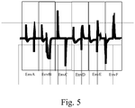
- the memory 202 comprises envelope signals as disclosed in Fig. 5
- Fig. 3 represents an algorithm executed according to the present invention.
- step S30 the input signal is received as disclosed in reference to Figs. 1a to 1d .
- the gate driver provides a gate signal VGmeas to the power semiconductor S1.
- the conditioner 10 provides the expected signal VGexp.
- the difference detection module 13 provides to the diagnostic module 10 a signal representative of the comparison of the gate signal VGmeas to the expected signal VGexp.
- the diagnostic module 10 analyses the signal received from the difference detection module 13.
- Fig. 4 represents examples of signals that can occur during the operation of a gate diver of a power semiconductor.
- signals VGmeas and VGexp are almost identical.
- the shape of signals VGmeas and VGexp are representative of a normal operation of the gate driver 12 and the power semiconductor S1.
- the output of the gate driver 12 provides a wrong logic level, the signal difference D saturates indicating a fault.
- the input characteristic of power semiconductor S1 presents a lower resistance (e.g. the gate resistance is short-circuited)
- the signal difference D indicates the anomaly as a short and high value pulses during the transitions. Furthermore, during the transition the difference signal D has opposite sign compared to the normal operation.
- the input characteristic of power semiconductor S1 presents a higher resistance (twice bigger than normal, the difference signal D indicates the anomaly as large and high value pulses.
- the difference signal D indicates a constant error that doesn't return to 0.
- the gate driver 12 has an abnormal delay time, the difference signal D indicates high values spikes during the transitions.
- the diagnostic module 10 may compare the difference signal D to a threshold in order to detect a deterioration, like for example the example given in the time intervals T2, T3 and T6.
- the value of the threshold is either pre-defined, or initially auto-defined like for example 120% the maximum value observed during the first 100 cycles of operation, or constantly auto-defined like for example 120% the maximum value observed until now.
- the diagnostic module 10 may integrate the difference signal D in order to detect a deterioration as the one disclosed in the time interval T5.
- the diagnostic module 10 may check if the signal D is within predetermined envelopes stored in memory in order to detect a deterioration.
- Fig. 5 represents examples of envelopes that are used by the diagnostic module for determining if a fault appears during the operation of the driver and of the power semiconductor.
- the envelope EnvA corresponds to a signal as shown in the time interval T1 of Fig. 4 .
- the envelope EnvB corresponds to a signal as shown in the time interval T2 of Fig. 4 .
- the envelope EnvC corresponds to a signal as shown in the time interval T3 of Fig. 4 .
- the envelope EnvD corresponds to a signal as shown in the time interval T4 of Fig. 4 .
- the envelope EnvE corresponds to a signal as shown in the time interval T5 of Fig. 4 .
- the envelope EnvF corresponds to a signal as shown in the time interval T6 of Fig. 4 .
- Fig. 6 represents mean, min, max and integral values corresponding to the differences observed when no deterioration occurs and when various different deteriorations occur.
- the calculations in the part noted calc1 correspond to calculations performed on the signal as shown in the time interval T1 of Fig. 4 .
- the calculation result noted Me1 corresponds to the mean of the signal as shown in the time interval T1
- the calculation result noted Mi1 corresponds to the minimum of the signal as shown in the time interval T1
- the calculation result noted Ma1 corresponds to the maximum of the signal as shown in the time interval T1
- the calculation result noted In1 corresponds to the integral of the signal as shown in the time interval T1.
- the calculations in the part noted calc2 correspond to calculations performed on the signal as shown in the time interval T2 of Fig. 4 .
- the calculation result noted Me2 corresponds to the mean of the signal as shown in the time interval T2
- the calculation result noted Mi2 corresponds to the minimum of the signal as shown in the time interval T2
- the calculation result noted Ma2 corresponds to the maximum of the signal as shown in the time interval T2
- the calculation result noted In2 corresponds to the integral of the signal as shown in the time interval T2.
- the calculations in the part noted calc3 correspond to calculations performed on the signal as shown in the time interval T3 of Fig. 4 .
- the calculation result noted Me3 corresponds to the mean of the signal as shown in the time interval T3
- the calculation result noted Mi3 corresponds to the minimum of the signal as shown in the time interval T3
- the calculation result noted Ma3 corresponds to the maximum of the signal as shown in the time interval T3
- the calculation result noted In3 corresponds to the integral of the signal as shown in the time interval T3.
- the calculations in the part noted calc4 correspond to calculations performed on the signal as shown in the time interval T4 of Fig. 4 .
- the calculation result noted Me4 corresponds to the mean of the signal as shown in the time interval T4
- the calculation result noted Mi4 corresponds to the minimum of the signal as shown in the time interval T4
- the calculation result noted Ma4 corresponds to the maximum of the signal as shown in the time interval T4
- the calculation result noted In4 corresponds to the integral of the signal as shown in the time interval T4.
- the calculations in the part noted calc5 correspond to calculations performed on the signal as shown in the time interval T5 of Fig. 4 .
- the calculation result noted Me5 corresponds to the mean of the signal as shown in the time interval T5
- the calculation result noted Mi5 corresponds to the minimum of the signal as shown in the time interval T5
- the calculation result noted Ma5 corresponds to the maximum of the signal as shown in the time interval T5
- the calculation result noted In5 corresponds to the integral of the signal as shown in the time interval T5.
- the calculations in the part noted calc6 correspond to calculations performed on the signal as shown in the time interval T6 of Fig. 4 .
- the calculation result noted Me6 corresponds to the mean of the signal as shown in the time interval T6
- the calculation result noted Mi6 corresponds to the minimum of the signal as shown in the time interval T6
- the calculation result noted Ma6 corresponds to the maximum of the signal as shown in the time interval T6
- the calculation result noted In6 corresponds to the integral of the signal as shown in the time interval T6.
- the value is considered as corresponding to no deterioration, otherwise the value is considered as corresponding to a deterioration.
- the minimum is superior to minus ten value, the value is considered as corresponding to no deterioration, otherwise the value is considered as corresponding to a deterioration.
- the maximum is superior to ten value, the value is considered as corresponding to no deterioration, otherwise the value is considered as corresponding to a deterioration.
- the integral value is superior to minus five, the value is considered as corresponding to no deterioration, otherwise the value is considered as corresponding to a deterioration.
- the comparison of these metrics to threshold values as the abovementioned one gives unique pattern that allows identifying a deterioration.
- the diagnostic module detects a deterioration if one of the comparisons shows a degradation.
- the diagnostic module may provide comparison results as an output signal.
- the alarm block 206 is activated or a signal Out is outputted in order to inform that a deterioration occurs, and which deterioration occurs.
- the difference signal D and/or the comparison results is or are memorized by the diagnostic module in order to provide data that may be useful for maintenance staff.
- the diagnostic module performs an initial validation of the communication with the gate driver.
- D VGexp
- the signal D is an image of the input signal.
Abstract
Description
- The present invention relates generally to a method and a system for device for monitoring the gate signal of a power semiconductor.
- In field applications such as traction, most of the failures on gate drivers of power semiconductors are reported as desaturation errors, i.e. the gate driver reports an abnormal condition wherein the gate voltage is at a high level and the voltage across the semiconductor is higher than a threshold value. The reporting of such anomaly is often a false positive, i.e. a problem is notified despite the gate driver and the power semiconductor operate normally. In some other cases, such reporting can be a true positive, i.e. when a short-circuit occurs.
- Short-circuits are typically caused by the gate driver itself, the controller, the power semiconductor, or the load. The usually implemented protection methods avoid a catastrophic failure but do not help the maintenance team to understand the source of the failure. In some cases where the gate driver is faulty, the whole system may be changed while only a low-cost replacement of the gate driver board would have solved the issue.
- It is thus important to monitor efficiently the operation of the gate driver itself, the operation of the power semiconductor, and to improve diagnostics.
- The present invention aims to allow an efficient monitoring of a gate driver and of a power semiconductor.
- To that end, the present invention concerns a device for monitoring the gate signal of a power semiconductor, the gate signal of the power semiconductor being provided by a gate driver, characterized in that the device comprises:
- means for generating an expected signal that corresponds to the signal outputted by the gate driver when no deterioration of the gate driver and/or of the power semiconductor and/or of a load linked to the power semiconductor exists,
- means for comparing the expected signal and the signal outputted by the gate driver,
- means for determining if a deterioration of the gate driver and/or of the power semiconductor and/or of a load linked to the power semiconductor exists using the result of the comparing of the expected signal and the signal outputted by the gate driver.
- The present invention concerns also a method for monitoring the gate signal of a power semiconductor, the gate signal of the power semiconductor being provided by a gate driver, characterized in that the method comprises the steps of:
- generating an expected signal that corresponds to the signal outputted by the gate driver when no deterioration of the gate driver and/or of the power semiconductor and/or of a load linked to the power semiconductor exists,
- comparing the expected signal and the signal outputted by the gate driver,
- determining if a deterioration of the gate driver and/or of the power semiconductor and/or of a load linked to the power semiconductor exists using the result of the comparing of the expected signal and the signal outputted by the gate driver.
- Thus, the anomalies in the gate signal trajectory are extracted at high speed during the commutation. The diagnostic is then improved.
- According to a particular feature, the means for generating the expected signal comprise at least a capacitor and a resistor.
- Thus, the implementation is performed with off-the-shelf and low-cost electronic components.
- According to a particular feature, the gate driver comprises a first isolation module and the output of the means for determining if a deterioration occurs is connected to a second isolation module.
- Thus, the requirements on the second isolation e.g. time response, bandwidth are low.
- According to a particular feature, the gate driver and means for generating an expected signal receive a pulse width modulated signal and a signal taken on a connection of the semiconductor that is different from the gate signal.
- Thus, gate drivers using a signal from the power semiconductor for protection or gate trajectory control can be diagnosed.
- According to a particular feature, the means for determining if the deterioration occurs process the result of the comparing of the expected signal and the signal outputted by the gate driver by comparing the result of the comparing to a threshold and/or by performing integration and/or mean and/or extreme values of the result of the comparing and comparing these integration and/or mean and/or extreme values to thresholds in order to detect a deterioration and/or by comparing the result of the comparing to stored envelopes of signals.
- Thus, the means for determining if the deterioration occurs can be implemented with high bandwidth analog circuits.
- According to a particular feature, the value of the at least one threshold is predetermined.
- Thus, the method is operational from the first operation of the power semiconductor and the designer can select the sensitivity to certain failures.
- According to a particular feature, the value of the at least one threshold is equal to X% the maximum value observed during the first 100 cycles of operation of the device, X being predefined and superior to 100%.
- Thus, the method does not require prior definition by the designer and adapts to the specificities of the system it is integrated in (e.g. power semi-conductor variabilities, operating conditions).
- According to a particular feature, the value of the threshold is equal to X% of the maximum value observed from the beginning of operation of the device, X being predefined and superior to 100%.
- Thus, the method detects sudden deterioration and does not detect progressive deterioration.
- The characteristics of the invention will emerge more clearly from a reading of the following description of example embodiments, the said description being produced with reference to the accompanying drawings, among which:
-
Fig. 1a represents a first example of an architecture of a gate driver of a power semiconductor in which the present invention is implemented; -
Fig. 1b represents a second example of an architecture of a gate driver of a power semiconductor in which the present invention is implemented; -
Fig. 1c represents a third example of an architecture of a gate driver of a power semiconductor in which the present invention is implemented; -
Fig. 1d represents a fourth example of an architecture of a gate driver of a power semiconductor in which the present invention is implemented; -
Fig. 2 is a diagram representing the architecture of a diagnostic module in which the present invention is implemented; -
Fig. 3 represents an algorithm executed according to the present invention; -
Fig. 4 represents examples of signals that can occur during the operation of a gate diver of a power semiconductor; -
Fig. 5 represents examples of envelopes that are used by the diagnostic module for determining if a fault appears during the operation of the driver and of the power semiconductor; -
Fig. 6 represents mean, min, max and integral values corresponding to the differences observed when no deterioration occurs and when various different deteriorations occur. -
Fig. 1a represents a first example of an architecture of a gate driver of a power semiconductor in which the present invention is implemented. - According to the first example of realization, a
conditioner 10a generates an expected gate signal VGexp from the input signal In provided to thegate driver 12a that provides a gate signal VGmeas to the power semiconductor S1. The gate signal VGmeas is compared to the expected gate driver signal VGexp by adifference detection module 13a in order to determine deviations of VGmeas and VGexp. The comparison may be a subtraction of one signal to the other signal and an amplification of the subtraction result. The output of thedifference detection module 13a is provided to adiagnostic module 14a that quantifies the output of thedifference detection module 13a using, for example, comparison with different kinds of signal envelopes, mathematical operations, e.g. max, mean and integral. - The generation by the
conditioner 10a of the expected gate signal VGexp can be tuned to reflect specificities relative to the power semi-conductor and/or operating conditions. The generation of VGexp is performed based on the input signal, using a model the transfer function of which reproduces the transfer function of thegate driver 12a in normal operation. - The input signal In is for example a PWM signal generated by an external controller not shown in
Fig. 1a . - The transfer function used by the
conditioner 10a is a circuit composed by a buffer, buf, which introduces a fixed delay, t1, and a RC circuit, VGexp is the voltage between the R and the C components. The R and/or the C values can be tuned depending of the power semiconductor S1. The fixed delay, t1, has the same value than the delay produced by thegate driver 12a. The time constant of the circuit RC is equal to the time constant of the typical gate resistor (internal plus external) and the equivalent input capacitance of the power semiconductor S1. For example, the value of the resistor is around 10Ω and the capacitance C is around 10nF. Theconditioner 10a may implement non-linear controlled capacitor and/or resistor values. - In a particular feature, the voltage supply of the
conditioner 10a is inferior to the voltage supply of thegate driver 12a by a divisor factor K. In this case, the voltage between R and C is amplified by a factor K. Thus, the power necessary to supply theconditioner 10a is reduced by a factor K2. - The expected signal VGexp is a signal that corresponds to the signal outputted by the gate driver when no deterioration of the gate driver and/or of the power semiconductor and/or of a load linked to the power semiconductor exist.
-
Fig. 1b represents a second example of an architecture of a gate driver of a power semiconductor in which the present invention is implemented. - According to the second example of realization, a
conditioner 10b generates an expected gate signal VGexp from the input signal In provided to thegate driver 12b that provides a gate signal VGmeas to the power semiconductor S1. The gate signal VGmeas is compared to the expected gate driver signal VGexp by adifference detection module 13b in order to determine deviations of VGmeas and VGexp. The comparison may be a subtraction of one signal to the other signal and an amplification of the subtraction result. The output of thedifference detection module 13b is provided to adiagnostic module 14b that quantifies the output of thedifference detection module 13b using, for example, comparison with different kinds of signal envelopes, mathematical operations, e.g. max, mean and integral. - The generation by the
conditioner 10b of the expected gate signal VGexp is controlled by thediagnostic module 14b in order to implement controlled capacitor and/or resistors values provided by the diagnostic module so as to represent more accurately the expected gate signal VGexp. Thediagnostic module 14b may select one transfer function out of several. Theconditioner 10b may generate the signal VGexp using a processing unit and a digital to analog converter based on a lookup table, a model or a transfer function provided by thediagnostic module 14b. - The expected signal VGexp is a signal that corresponds to the signal outputted by the gate driver with no deterioration of the gate driver and/or of the power semiconductor and/or of a load linked to the power semiconductor exist.
-
Fig. 1c represents a third example of an architecture of a gate driver of a power semiconductor in which the present invention is implemented. - According to the third example of realization, a
conditioner 10c generates an expected gate signal VGexp from the input signal In provided to thegate driver 12c that provides a gate signal VGmeas to the power semiconductor S1. The gate signal VGmeas is compared to the expected gate driver signal VGexp by adifference detection module 13c in order to determine deviations of VGmeas and VGexp. The comparison may be a subtraction of one signal to the other signal and an amplification of the subtraction result. The output of thedifference detection module 13c is provided to adiagnostic module 14c that quantifies the output of thedifference detection module 13c using, for example, comparison with different kinds of signal envelopes, mathematical operations, e.g. max, mean and integral. - The generation by the
conditioner 10c of the expected gate signal VGexp may be as the one disclosed inFig. 1a or 1b with a particular processing that takes into account the feedback signal. - The input signal In is for example a PWM signal generated by an external controller not shown in
Fig. 1c . - In the third example of realization, the
gate driver 12c uses the input signal In together with a feedback signal from the power semiconductor. One example of feedback signal is the collector voltage of the power semiconductor that can be used for protection and/or active gate signal trajectory control. The feedback signal is typically combined with the PWM signal by thegate driver 12c and theconditioner 10c. - The generation by the
conditioner 10c of the expected gate signal VGexp may be as the one disclosed inFig. 1a or 1b with a particular processing that takes into account the feedback signal. - The expected signal VGexp is a signal that corresponds to the signal outputted by the gate driver when no deterioration of the gate driver and/or of the power semiconductor and/or of a load linked to the power semiconductor exist.
-
Fig. 1d represents a fourth example of an architecture of a gate driver of a power semiconductor in which the present invention is implemented. - According to the fourth example of realization, a
conditioner 10d generates an expected gate signal VGexp from the input signal In provided to thegate driver 12d that provides a gate signal VGmeas to the power semiconductor S1. The gate signal VGmeas is compared to the expected gate driver signal VGexp by adifference detection module 13d in order to determine deviations of VGmeas and VGexp. The comparison may be a subtraction of one signal to the other signal and an amplification of the subtraction result. The output of thedifference detection module 13d is provided to adiagnostic module 14d that quantifies the output of thedifference detection module 13d using, for example, comparison with different kinds of signal envelopes, mathematical operations, e.g. max, mean and integral. - The input signal In is for example a PWM signal generated by an external controller not shown in
Fig. 1d . - In the example of
Fig. 1d , thedriver 12c is composed of a preprocessing module Pr, an insulation module Is and a buffer Bu. The output of the insulation module Is is provided to theconditioner 10d as an input signal. - A second insulation module Is2 is provided at the output of the
diagnostic module 14d. - The expected signal VGexp is a signal that corresponds to the signal outputted by the gate driver when no deterioration of the gate driver and/or of the power semiconductor and/or of a load linked to the power semiconductor exist.
-
Fig. 2 is a diagram representing the architecture of the diagnostic module in which the present invention is implemented. - The
diagnostic module 10, that can be either 10a, 10b, 10c or 10d has, for example, an architecture based on components connected together by abus 201 and aprocessor 200 controlled by the program as disclosed inFig. 3 . - The
bus 201 links theprocessor 200 to a read onlymemory ROM 202, a randomaccess memory RAM 203, aninput output interface 205 and eventually analarm module 206. - The
memory 203 contains registers intended to receive variables and the instructions of the programs related to the algorithm as disclosed inFig. 3 . - The read only
memory 202 contains instructions of the programs related to the algorithm as disclosed inFigs. 3 , which are transferred, when thediagnostic module 10 is powered on, to therandom access memory 203. - Any and all steps of the algorithm described hereafter with regard to
Fig. 3 may be implemented in software by execution of a set of instructions or program by a programmable computing machine, such as a PC (Personal Computer), a DSP (Digital Signal Processor) or a microcontroller; or else implemented in hardware by a machine or a dedicated component, such as an FPGA (Field-Programmable Gate Array) or an ASIC (Application-Specific Integrated Circuit). - In other words, the
diagnostic module 10 includes circuitry, or a device including circuitry, causing thediagnostic module 10 to perform the steps of the algorithms described hereafter with regard toFig. 3 . - The
memory 202 comprises envelope signals as disclosed inFig. 5 -
Fig. 3 represents an algorithm executed according to the present invention. - At step S30, the input signal is received as disclosed in reference to
Figs. 1a to 1d . - At step S31, the gate driver provides a gate signal VGmeas to the power semiconductor S1.
- At step S32, the
conditioner 10 provides the expected signal VGexp. - At step S33, the difference detection module 13 provides to the
diagnostic module 10 a signal representative of the comparison of the gate signal VGmeas to the expected signal VGexp. - At step S34, the
diagnostic module 10 analyses the signal received from the difference detection module 13. - Examples of signals received from the difference detection module 13 are given in
Fig. 4 . -
Fig. 4 represents examples of signals that can occur during the operation of a gate diver of a power semiconductor. - In
Fig. 4 the signals In, VGmeas, VGexp, the signal D, which is the signal at the output of the difference detection module 13, are shown during different intervals noted T1 to T6. - In the time interval T1, the signals VGmeas and VGexp are almost identical. The shape of signals VGmeas and VGexp are representative of a normal operation of the gate driver 12 and the power semiconductor S1.
- In the time interval T2, the output of the gate driver 12 provides a wrong logic level, the signal difference D saturates indicating a fault.
- In the time interval T3, the input characteristic of power semiconductor S1 presents a lower resistance (e.g. the gate resistance is short-circuited), the signal difference D indicates the anomaly as a short and high value pulses during the transitions. Furthermore, during the transition the difference signal D has opposite sign compared to the normal operation.
- In the time interval T4, the input characteristic of power semiconductor S1 presents a higher resistance (twice bigger than normal, the difference signal D indicates the anomaly as large and high value pulses.
- In the time interval T5, the power supply level of the gate driver 12 has a droop, the difference signal D indicates a constant error that doesn't return to 0.
- In the time interval T6, the gate driver 12 has an abnormal delay time, the difference signal D indicates high values spikes during the transitions.
- The
diagnostic module 10 may compare the difference signal D to a threshold in order to detect a deterioration, like for example the example given in the time intervals T2, T3 and T6. The value of the threshold is either pre-defined, or initially auto-defined like for example 120% the maximum value observed during the first 100 cycles of operation, or constantly auto-defined like for example 120% the maximum value observed until now. Thediagnostic module 10 may integrate the difference signal D in order to detect a deterioration as the one disclosed in the time interval T5. Thediagnostic module 10 may check if the signal D is within predetermined envelopes stored in memory in order to detect a deterioration. - Examples of such envelopes are given in
Fig. 5 . -
Fig. 5 represents examples of envelopes that are used by the diagnostic module for determining if a fault appears during the operation of the driver and of the power semiconductor. - The envelope EnvA corresponds to a signal as shown in the time interval T1 of
Fig. 4 . - The envelope EnvB corresponds to a signal as shown in the time interval T2 of
Fig. 4 . - The envelope EnvC corresponds to a signal as shown in the time interval T3 of
Fig. 4 . - The envelope EnvD corresponds to a signal as shown in the time interval T4 of
Fig. 4 . - The envelope EnvE corresponds to a signal as shown in the time interval T5 of
Fig. 4 . - The envelope EnvF corresponds to a signal as shown in the time interval T6 of
Fig. 4 . -
Fig. 6 represents mean, min, max and integral values corresponding to the differences observed when no deterioration occurs and when various different deteriorations occur. - The calculations in the part noted calc1 correspond to calculations performed on the signal as shown in the time interval T1 of
Fig. 4 . - The calculation result noted Me1 corresponds to the mean of the signal as shown in the time interval T1, the calculation result noted Mi1 corresponds to the minimum of the signal as shown in the time interval T1, the calculation result noted Ma1 corresponds to the maximum of the signal as shown in the time interval T1 and the calculation result noted In1 corresponds to the integral of the signal as shown in the time interval T1.
- The calculations in the part noted calc2 correspond to calculations performed on the signal as shown in the time interval T2 of
Fig. 4 . - The calculation result noted Me2 corresponds to the mean of the signal as shown in the time interval T2, the calculation result noted Mi2 corresponds to the minimum of the signal as shown in the time interval T2, the calculation result noted Ma2 corresponds to the maximum of the signal as shown in the time interval T2 and the calculation result noted In2 corresponds to the integral of the signal as shown in the time interval T2.
- The calculations in the part noted calc3 correspond to calculations performed on the signal as shown in the time interval T3 of
Fig. 4 . - The calculation result noted Me3 corresponds to the mean of the signal as shown in the time interval T3, the calculation result noted Mi3 corresponds to the minimum of the signal as shown in the time interval T3, the calculation result noted Ma3 corresponds to the maximum of the signal as shown in the time interval T3 and the calculation result noted In3 corresponds to the integral of the signal as shown in the time interval T3.
- The calculations in the part noted calc4 correspond to calculations performed on the signal as shown in the time interval T4 of
Fig. 4 . - The calculation result noted Me4 corresponds to the mean of the signal as shown in the time interval T4, the calculation result noted Mi4 corresponds to the minimum of the signal as shown in the time interval T4, the calculation result noted Ma4 corresponds to the maximum of the signal as shown in the time interval T4 and the calculation result noted In4 corresponds to the integral of the signal as shown in the time interval T4.
- The calculations in the part noted calc5 correspond to calculations performed on the signal as shown in the time interval T5 of
Fig. 4 . - The calculation result noted Me5 corresponds to the mean of the signal as shown in the time interval T5, the calculation result noted Mi5 corresponds to the minimum of the signal as shown in the time interval T5, the calculation result noted Ma5 corresponds to the maximum of the signal as shown in the time interval T5 and the calculation result noted In5 corresponds to the integral of the signal as shown in the time interval T5.
- The calculations in the part noted calc6 correspond to calculations performed on the signal as shown in the time interval T6 of
Fig. 4 . - The calculation result noted Me6 corresponds to the mean of the signal as shown in the time interval T6, the calculation result noted Mi6 corresponds to the minimum of the signal as shown in the time interval T6, the calculation result noted Ma6 corresponds to the maximum of the signal as shown in the time interval T6 and the calculation result noted In6 corresponds to the integral of the signal as shown in the time interval T6.
- For example, if the mean is superior to null value, the value is considered as corresponding to no deterioration, otherwise the value is considered as corresponding to a deterioration. If the minimum is superior to minus ten value, the value is considered as corresponding to no deterioration, otherwise the value is considered as corresponding to a deterioration. If the maximum is superior to ten value, the value is considered as corresponding to no deterioration, otherwise the value is considered as corresponding to a deterioration. If the integral value is superior to minus five, the value is considered as corresponding to no deterioration, otherwise the value is considered as corresponding to a deterioration.
- These calculations can be implemented with simple fast analog circuits. The comparison of these metrics to threshold values as the abovementioned one gives unique pattern that allows identifying a deterioration. The diagnostic module detects a deterioration if one of the comparisons shows a degradation. The diagnostic module may provide comparison results as an output signal.
- As a result, if a deterioration occurs, the
alarm block 206 is activated or a signal Out is outputted in order to inform that a deterioration occurs, and which deterioration occurs. - If such deterioration occurs, the difference signal D and/or the comparison results is or are memorized by the diagnostic module in order to provide data that may be useful for maintenance staff.
- In a variant of operation, the diagnostic module performs an initial validation of the communication with the gate driver. In this mode, the gate driver is deactivated such that VGmeas=0. Thus, D=VGexp, the signal D is an image of the input signal. Thus, in case of a misconnection of the input or output signal, or in case of a default in the conditioner, an anomaly is easily detected.
- Naturally, many modifications can be made to the embodiments of the invention described above without departing from the scope of the present invention.
Claims (9)
- A device for monitoring the gate signal of a power semiconductor, the gate signal of the power semiconductor being provided by a gate driver, characterized in that the device comprises:- means for generating an expected reference signal that corresponds to the signal outputted by the gate driver when no deterioration of the gate driver and/or of the power semiconductor and/or of a load linked to the power semiconductor exists,- means for comparing the expected reference signal and the signal outputted by the gate driver,- means for determining if a deterioration of the gate driver and/or of the power semiconductor and/or of a load linked to the power semiconductor exists using the result of the comparing of the reference expected signal and the signal outputted by the gate driver.
- The device according to claim 1, characterized in that the means for generating the expected reference signal comprise at least a first order model composed of a capacitor and a resistor.
- The device according to claim 1 or 2, characterized in that the gate driver comprises a first isolation module and the output of the means for determining if a deterioration occurs is connected to a second isolation module.
- The device according to any of the claims 1 to 3, characterized in that the gate driver and means for generating an expected signal receive a pulse width modulated signal and a signal taken on a connection of the semiconductor that is different from the gate signal.
- The device according to any of the claims 1 to 4, characterized in that the means for determining if the deterioration occurs process the result of the comparison of the expected signal and the signal outputted by the gate driver by comparing the result of the comparison to a threshold and/or by performing integration and/or mean and/or extreme values of the result of the comparison and comparing the integration and/or mean and/or extreme values to thresholds and/or by comparing the result of the comparing to stored envelopes of signals.
- The device according to claim 5, characterized in that the value of the at least one threshold is predetermined.
- The device according to claim 5, characterized in that the value of the at least one threshold is equal to X% of the maximum value observed during the first 100 cycles of operation of the device, X being predefined and superior to 100%.
- The device according to claim 5, characterized in that the value of the threshold is equal to X% of the maximum value observed from the beginning of operation of the device, X being predefined and superior to 100%.
- A method for monitoring the gate signal of a power semiconductor, the gate signal of the power semiconductor being provided by a gate driver, characterized in that the method comprises the steps of:- generating an expected reference signal that corresponds to the signal outputted by the gate driver when no deterioration of the gate driver and/or of the power semiconductor and/or of a load linked to the power semiconductor exists,- comparing the expected reference signal and the signal outputted by the gate driver,- determining if a deterioration of the gate driver and/or of the power semiconductor and/or of a load linked to the power semiconductor exists using the result of the comparing of the expected reference signal and the signal outputted by the gate driver.
Priority Applications (5)
| Application Number | Priority Date | Filing Date | Title |
|---|---|---|---|
| EP19160277.0A EP3702793A1 (en) | 2019-03-01 | 2019-03-01 | A method and a device for monitoring the gate signal of a power semiconductor |
| US17/422,383 US20220091177A1 (en) | 2019-03-01 | 2020-01-16 | Method and device for monitoring gate signal of power semiconductor |
| CN202080015436.1A CN113474667A (en) | 2019-03-01 | 2020-01-16 | Method and device for monitoring grid signals of power semiconductor |
| PCT/JP2020/002199 WO2020179263A1 (en) | 2019-03-01 | 2020-01-16 | Method and device for monitoring gate signal of power semiconductor |
| JP2021552088A JP7210763B2 (en) | 2019-03-01 | 2020-01-16 | METHOD AND DEVICE FOR MONITORING GATE SIGNAL OF POWER SEMICONDUCTOR |
Applications Claiming Priority (1)
| Application Number | Priority Date | Filing Date | Title |
|---|---|---|---|
| EP19160277.0A EP3702793A1 (en) | 2019-03-01 | 2019-03-01 | A method and a device for monitoring the gate signal of a power semiconductor |
Publications (1)
| Publication Number | Publication Date |
|---|---|
| EP3702793A1 true EP3702793A1 (en) | 2020-09-02 |
Family
ID=65657374
Family Applications (1)
| Application Number | Title | Priority Date | Filing Date |
|---|---|---|---|
| EP19160277.0A Pending EP3702793A1 (en) | 2019-03-01 | 2019-03-01 | A method and a device for monitoring the gate signal of a power semiconductor |
Country Status (5)
| Country | Link |
|---|---|
| US (1) | US20220091177A1 (en) |
| EP (1) | EP3702793A1 (en) |
| JP (1) | JP7210763B2 (en) |
| CN (1) | CN113474667A (en) |
| WO (1) | WO2020179263A1 (en) |
Cited By (2)
| Publication number | Priority date | Publication date | Assignee | Title |
|---|---|---|---|---|
| CN112781174A (en) * | 2020-12-31 | 2021-05-11 | 青岛海信日立空调系统有限公司 | Variable frequency air conditioner and variable frequency air conditioner service life monitoring control method |
| US11889246B1 (en) | 2022-07-05 | 2024-01-30 | Infineon Technologies Ag | Electronic device and electronic system that receives and processes telemetry information |
Families Citing this family (1)
| Publication number | Priority date | Publication date | Assignee | Title |
|---|---|---|---|---|
| JP7341370B1 (en) | 2022-10-11 | 2023-09-08 | 三菱電機株式会社 | power converter |
Citations (2)
| Publication number | Priority date | Publication date | Assignee | Title |
|---|---|---|---|---|
| EP3261215A1 (en) * | 2016-06-21 | 2017-12-27 | Hamilton Sundstrand Corporation | Fault detection system for isolated two-switch exciter drive gate driver |
| US20180102773A1 (en) * | 2016-10-07 | 2018-04-12 | Texas Instruments Incorporated | Gate Driver with VGTH and VCESAT Measurement Capability for the State of Health Monitor |
Family Cites Families (10)
| Publication number | Priority date | Publication date | Assignee | Title |
|---|---|---|---|---|
| JPS60131479A (en) * | 1983-12-20 | 1985-07-13 | Oki Electric Ind Co Ltd | Testing device for semiconductor device |
| JPS61262671A (en) * | 1985-04-19 | 1986-11-20 | Kawasaki Erekutoronika Kk | Function testing method and function tester |
| JP3931627B2 (en) * | 2001-11-01 | 2007-06-20 | 株式会社日立製作所 | Gate driving device for semiconductor switching element |
| US8823411B2 (en) * | 2010-02-08 | 2014-09-02 | Freescale Semiconductor, Inc. | Fatal failure diagnostics circuit and methodology |
| JP5415993B2 (en) * | 2010-02-26 | 2014-02-12 | 古河電気工業株式会社 | Power supply device |
| JP5750311B2 (en) * | 2011-05-31 | 2015-07-22 | 日立オートモティブシステムズ株式会社 | Inverter drive |
| CN104237761B (en) * | 2013-06-13 | 2018-05-04 | 通用电气公司 | The system and method for the failure mode detection and protection of insulated gate bipolar transistor |
| US9322852B2 (en) * | 2014-07-15 | 2016-04-26 | Ford Global Technologies, Llc | Gate drive under-voltage detection |
| US10126353B2 (en) * | 2015-03-23 | 2018-11-13 | Infineon Technologies Ag | Verification of gate driver protection logic |
| JPWO2018168328A1 (en) * | 2017-03-14 | 2020-01-16 | 日本電産株式会社 | Power semiconductor switching device damage prediction device and damage prediction method, AC-DC converter, DC-DC converter |
-
2019
- 2019-03-01 EP EP19160277.0A patent/EP3702793A1/en active Pending
-
2020
- 2020-01-16 WO PCT/JP2020/002199 patent/WO2020179263A1/en active Application Filing
- 2020-01-16 US US17/422,383 patent/US20220091177A1/en active Pending
- 2020-01-16 JP JP2021552088A patent/JP7210763B2/en active Active
- 2020-01-16 CN CN202080015436.1A patent/CN113474667A/en active Pending
Patent Citations (2)
| Publication number | Priority date | Publication date | Assignee | Title |
|---|---|---|---|---|
| EP3261215A1 (en) * | 2016-06-21 | 2017-12-27 | Hamilton Sundstrand Corporation | Fault detection system for isolated two-switch exciter drive gate driver |
| US20180102773A1 (en) * | 2016-10-07 | 2018-04-12 | Texas Instruments Incorporated | Gate Driver with VGTH and VCESAT Measurement Capability for the State of Health Monitor |
Cited By (3)
| Publication number | Priority date | Publication date | Assignee | Title |
|---|---|---|---|---|
| CN112781174A (en) * | 2020-12-31 | 2021-05-11 | 青岛海信日立空调系统有限公司 | Variable frequency air conditioner and variable frequency air conditioner service life monitoring control method |
| CN112781174B (en) * | 2020-12-31 | 2023-11-21 | 青岛海信日立空调系统有限公司 | Variable frequency air conditioner and service life monitoring control method thereof |
| US11889246B1 (en) | 2022-07-05 | 2024-01-30 | Infineon Technologies Ag | Electronic device and electronic system that receives and processes telemetry information |
Also Published As
| Publication number | Publication date |
|---|---|
| WO2020179263A1 (en) | 2020-09-10 |
| JP7210763B2 (en) | 2023-01-23 |
| JP2022509565A (en) | 2022-01-20 |
| US20220091177A1 (en) | 2022-03-24 |
| CN113474667A (en) | 2021-10-01 |
Similar Documents
| Publication | Publication Date | Title |
|---|---|---|
| US20220091177A1 (en) | Method and device for monitoring gate signal of power semiconductor | |
| US10476386B2 (en) | Digitally controlled power supply apparatus and production management system | |
| JP4418197B2 (en) | Overvoltage protection circuit and power supply, power supply system and electronic device using the same | |
| KR102021864B1 (en) | Driving circuit of switching device for electric power control | |
| JP2016080532A (en) | Power supply voltage detection device | |
| KR20210075479A (en) | Sensor fault diagnosis system for converter | |
| KR20150084613A (en) | Method For Predicting Disorder Of Tower Crane By Using Data Mining | |
| US8044624B2 (en) | Load control apparatus and method for processing diagnosis signal for the same | |
| JP6612583B2 (en) | Open / Circuit detection circuit | |
| US7472337B2 (en) | Method and system for detecting faults in an electronic engine control module | |
| CN104044632A (en) | Cross Check Strategy For Systematic Error Protection | |
| US10126375B2 (en) | Diagnosis circuit and method for a power module | |
| JP3953093B2 (en) | A / D converter | |
| US20060291376A1 (en) | Continuous Median Failure Control System and Method | |
| US6535028B1 (en) | Data bus fault detection circuit and method | |
| JP2021005637A (en) | Control device | |
| US10673370B2 (en) | Three-phase motor control circuit and three-phase motor control method | |
| US20210036667A1 (en) | Semiconductor device | |
| EP4068549A1 (en) | Power supply system and power supply device | |
| TW202018319A (en) | Fan diagnosis circuit | |
| CN114356617B (en) | Error injection testing method, device, system and computing equipment | |
| JP7329579B2 (en) | Control device | |
| US10234882B2 (en) | Electrical function group | |
| JP2018152391A (en) | Semiconductor device | |
| US20160077943A1 (en) | Input module for programmable logic controller |
Legal Events
| Date | Code | Title | Description |
|---|---|---|---|
| PUAI | Public reference made under article 153(3) epc to a published international application that has entered the european phase |
Free format text: ORIGINAL CODE: 0009012 |
|
| STAA | Information on the status of an ep patent application or granted ep patent |
Free format text: STATUS: THE APPLICATION HAS BEEN PUBLISHED |
|
| AK | Designated contracting states |
Kind code of ref document: A1 Designated state(s): AL AT BE BG CH CY CZ DE DK EE ES FI FR GB GR HR HU IE IS IT LI LT LU LV MC MK MT NL NO PL PT RO RS SE SI SK SM TR |
|
| AX | Request for extension of the european patent |
Extension state: BA ME |
|
| STAA | Information on the status of an ep patent application or granted ep patent |
Free format text: STATUS: REQUEST FOR EXAMINATION WAS MADE |
|
| 17P | Request for examination filed |
Effective date: 20210302 |
|
| RBV | Designated contracting states (corrected) |
Designated state(s): AL AT BE BG CH CY CZ DE DK EE ES FI FR GB GR HR HU IE IS IT LI LT LU LV MC MK MT NL NO PL PT RO RS SE SI SK SM TR |
|
| STAA | Information on the status of an ep patent application or granted ep patent |
Free format text: STATUS: EXAMINATION IS IN PROGRESS |
|
| 17Q | First examination report despatched |
Effective date: 20221214 |