EP3699954A1 - Manufacturing method of tft substrate and tft substrate - Google Patents
Manufacturing method of tft substrate and tft substrate Download PDFInfo
- Publication number
- EP3699954A1 EP3699954A1 EP17929206.5A EP17929206A EP3699954A1 EP 3699954 A1 EP3699954 A1 EP 3699954A1 EP 17929206 A EP17929206 A EP 17929206A EP 3699954 A1 EP3699954 A1 EP 3699954A1
- Authority
- EP
- European Patent Office
- Prior art keywords
- layer
- silicon
- structures
- wafer
- plate
- Prior art date
- Legal status (The legal status is an assumption and is not a legal conclusion. Google has not performed a legal analysis and makes no representation as to the accuracy of the status listed.)
- Granted
Links
Images



Classifications
-
- H—ELECTRICITY
- H10—SEMICONDUCTOR DEVICES; ELECTRIC SOLID-STATE DEVICES NOT OTHERWISE PROVIDED FOR
- H10D—INORGANIC ELECTRIC SEMICONDUCTOR DEVICES
- H10D86/00—Integrated devices formed in or on insulating or conducting substrates, e.g. formed in silicon-on-insulator [SOI] substrates or on stainless steel or glass substrates
- H10D86/01—Manufacture or treatment
- H10D86/021—Manufacture or treatment of multiple TFTs
-
- H—ELECTRICITY
- H10—SEMICONDUCTOR DEVICES; ELECTRIC SOLID-STATE DEVICES NOT OTHERWISE PROVIDED FOR
- H10D—INORGANIC ELECTRIC SEMICONDUCTOR DEVICES
- H10D86/00—Integrated devices formed in or on insulating or conducting substrates, e.g. formed in silicon-on-insulator [SOI] substrates or on stainless steel or glass substrates
- H10D86/01—Manufacture or treatment
- H10D86/021—Manufacture or treatment of multiple TFTs
- H10D86/0212—Manufacture or treatment of multiple TFTs comprising manufacture, treatment or coating of substrates
-
- H—ELECTRICITY
- H10—SEMICONDUCTOR DEVICES; ELECTRIC SOLID-STATE DEVICES NOT OTHERWISE PROVIDED FOR
- H10P—GENERIC PROCESSES OR APPARATUS FOR THE MANUFACTURE OR TREATMENT OF DEVICES COVERED BY CLASS H10
- H10P90/00—Preparation of wafers not covered by a single main group of this subclass, e.g. wafer reinforcement
- H10P90/19—Preparing inhomogeneous wafers
- H10P90/1904—Preparing vertically inhomogeneous wafers
- H10P90/1906—Preparing SOI wafers
- H10P90/1914—Preparing SOI wafers using bonding
-
- H—ELECTRICITY
- H10—SEMICONDUCTOR DEVICES; ELECTRIC SOLID-STATE DEVICES NOT OTHERWISE PROVIDED FOR
- H10D—INORGANIC ELECTRIC SEMICONDUCTOR DEVICES
- H10D86/00—Integrated devices formed in or on insulating or conducting substrates, e.g. formed in silicon-on-insulator [SOI] substrates or on stainless steel or glass substrates
- H10D86/01—Manufacture or treatment
- H10D86/021—Manufacture or treatment of multiple TFTs
- H10D86/0221—Manufacture or treatment of multiple TFTs comprising manufacture, treatment or patterning of TFT semiconductor bodies
-
- H—ELECTRICITY
- H10—SEMICONDUCTOR DEVICES; ELECTRIC SOLID-STATE DEVICES NOT OTHERWISE PROVIDED FOR
- H10D—INORGANIC ELECTRIC SEMICONDUCTOR DEVICES
- H10D86/00—Integrated devices formed in or on insulating or conducting substrates, e.g. formed in silicon-on-insulator [SOI] substrates or on stainless steel or glass substrates
- H10D86/01—Manufacture or treatment
- H10D86/021—Manufacture or treatment of multiple TFTs
- H10D86/0231—Manufacture or treatment of multiple TFTs using masks, e.g. half-tone masks
-
- H—ELECTRICITY
- H10—SEMICONDUCTOR DEVICES; ELECTRIC SOLID-STATE DEVICES NOT OTHERWISE PROVIDED FOR
- H10D—INORGANIC ELECTRIC SEMICONDUCTOR DEVICES
- H10D86/00—Integrated devices formed in or on insulating or conducting substrates, e.g. formed in silicon-on-insulator [SOI] substrates or on stainless steel or glass substrates
- H10D86/40—Integrated devices formed in or on insulating or conducting substrates, e.g. formed in silicon-on-insulator [SOI] substrates or on stainless steel or glass substrates characterised by multiple TFTs
-
- H—ELECTRICITY
- H10—SEMICONDUCTOR DEVICES; ELECTRIC SOLID-STATE DEVICES NOT OTHERWISE PROVIDED FOR
- H10W—GENERIC PACKAGES, INTERCONNECTIONS, CONNECTORS OR OTHER CONSTRUCTIONAL DETAILS OF DEVICES COVERED BY CLASS H10
- H10W10/00—Isolation regions in semiconductor bodies between components of integrated devices
- H10W10/10—Isolation regions comprising dielectric materials
- H10W10/181—Semiconductor-on-insulator [SOI] isolation regions, e.g. buried oxide regions of SOI wafers
-
- H—ELECTRICITY
- H10—SEMICONDUCTOR DEVICES; ELECTRIC SOLID-STATE DEVICES NOT OTHERWISE PROVIDED FOR
- H10D—INORGANIC ELECTRIC SEMICONDUCTOR DEVICES
- H10D86/00—Integrated devices formed in or on insulating or conducting substrates, e.g. formed in silicon-on-insulator [SOI] substrates or on stainless steel or glass substrates
- H10D86/40—Integrated devices formed in or on insulating or conducting substrates, e.g. formed in silicon-on-insulator [SOI] substrates or on stainless steel or glass substrates characterised by multiple TFTs
- H10D86/411—Integrated devices formed in or on insulating or conducting substrates, e.g. formed in silicon-on-insulator [SOI] substrates or on stainless steel or glass substrates characterised by multiple TFTs characterised by materials, geometry or structure of the substrates
-
- H—ELECTRICITY
- H10—SEMICONDUCTOR DEVICES; ELECTRIC SOLID-STATE DEVICES NOT OTHERWISE PROVIDED FOR
- H10D—INORGANIC ELECTRIC SEMICONDUCTOR DEVICES
- H10D86/00—Integrated devices formed in or on insulating or conducting substrates, e.g. formed in silicon-on-insulator [SOI] substrates or on stainless steel or glass substrates
- H10D86/40—Integrated devices formed in or on insulating or conducting substrates, e.g. formed in silicon-on-insulator [SOI] substrates or on stainless steel or glass substrates characterised by multiple TFTs
- H10D86/60—Integrated devices formed in or on insulating or conducting substrates, e.g. formed in silicon-on-insulator [SOI] substrates or on stainless steel or glass substrates characterised by multiple TFTs wherein the TFTs are in active matrices
Definitions
- the present disclosure generally relates to the display panel manufacturing field, and in particular to a TFT substrate and a method for manufacturing the same.
- the flexible display panel is a deformable and bendable display apparatus.
- the flexible display panel may be applied into the electronic paper, LCD, OLED etc.
- An OLED (organic light-emitting diode) flexible display panel has the advantages, such as, low consumption, thin thickness and rollable ability, thus it largely attracts the peoples' eyes.
- the OLED flexible display panel may include a flexible substrate, OLED display components and connecting lines for connecting the OLED display components.
- the OLED display components may include an anode electrode, a cathode electrode opposite to the anode electrode and a functional layer between the anode electrode and the cathode electrode.
- the OLED display panel is lighted by means of the semiconductor material and the organic light-emitting material being driven by the electric field between the anode electrode and the cathode electrode, to inject or recombine the carries.
- a polyimide (PI) flexible substrate is a type of flexible substrate with good bendability and temperature resistance. Therefore it is widely used as the substrate of the OLED flexible display panel.
- the flexible substrate may be designed to have island structures. However, it is difficult to form the island structures on a polyimide flexible substrate.
- the present disclosure aims to provide a TFT substrate and a method for manufacturing the same to form the island structures on a substrate so as to improve the stability of the substrate during bending.
- a technical scheme adopted by the present disclosure is to provide a method for manufacturing a TFT substrate.
- the method comprises: providing a silicon-wafer plate; coating the silicon-wafer plate with a layer of photoresist material; patterning the photoresist material and removing a portion of the photoresist material where first masking structures are to be set; forming a first masking layer on a side of the silicon-wafer plate which is coated with the photoresist material, wherein the first masking layer covers the photoresist material; removing a portion of the first masking layer which covers the photoresist material with an etching solution corresponding to the photoresist material so as to forming the first mask; plasma etching the silicon-wafer plate to form island structures; cutting the island structures layer by layer to form a silicon-wafer sub-plate; and attaching the silicon-wafer sub-plate onto a substrate to form the TFT substrate.
- Another technical scheme adopted by the present disclosure is to provide a method for manufacturing a TFT substrate.
- the method comprises: providing a silicon-wafer plate; forming first masking structures on the silicon-wafer plate and etching to form island structures; cutting the island structures layer by layer to form a silicon-wafer sub-plate; and attaching the silicon-wafer sub-plate on a substrate to form the TFT substrate.
- the TFT substrate is manufactured by the above-mentioned method.
- the method comprises: providing a silicon-wafer plate; forming first masking structures on the silicon-wafer plate and etching to form island structures; cutting the island structures layer by layer to form a silicon-wafer sub-plate; and attaching the silicon-wafer sub-plate on a substrate to form the TFT substrate.
- the method of the present disclosure may include forming first masking structures on a silicon-wafer substrate, etching to form island structures, cutting layer by layer the island structures and then attaching onto a substrate to form a TFT substrate. Therefore, the implementation of the present disclosure may improve the stability of the substrate during bending and reduce the stress mismatch between the substrate and a TFT component film.
- a technical scheme adopted by the present disclosure is to provide a method for manufacturing a TFT substrate.
- the method comprises: providing a silicon-wafer plate; forming first masking structures on the silicon-wafer plate and plasma etching to form island structures; cutting the island structures layer by layer to form a silicon-wafer sub-plate; attaching the silicon-wafer sub-plate on a substrate to form the TFT substrate.
- the method will be depicted in detail as follows.
- FIG. 1 is a flow chart of the method for manufacturing a TFT substrate according to an embodiment of the present disclosure.
- a silicon-wafer plate may be taken as material to prepare the island structures to be attached on the flexible substrate.
- materials having similar molecular structure as the silicon-wafer which may match the flexible substrate, such as the chemical elements in the same family of silicon, may also be utilized to prepare the island elements.
- S102 Forming first masking structures on the silicon-wafer plate and etching to form island structures.
- a metal layer may be deposited as first masking structures on the silicon-wafer plate. Then the island structures may be formed by etching the silicon-wafer plate.
- the metal layer may be a layer of nickel.
- the island structures on the silicon-wafer plate may be cut layer by layer according to the structure and size of the island structures to be formed on the TFT substrate, so as to obtain silicon-wafer sub-plates as the island structures on the substrate.
- S104 Attaching the silicon-wafer sub-plate onto the substrate to form the TFT substrate.
- the substrate may be a polyimide (PI) flexible substrate.
- PI polyimide
- the polyimide flexible substrate itself has a certain adhesive capacity.
- the silicon-wafer sub-plates may be attached onto the polyimide flexible substrate with the help of the adhesive capacity of the polyimide flexible substrate.
- the silicon-wafer sub-plate may be taken as the island structures matching TFT components in order to manufacture the TFT substrate.
- the present disclosure provides a method including forming first masking structures on a silicon-wafer substrate, etching the silicon-wafer substrate via the first masking structures to form island structures, cutting layer by layer the island structures and then attaching them onto a substrate to form the TFT substrate. Therefore, the implementation of the present disclosure may improve the stability of the substrate during bending and reduce the stress mismatch between the substrate and a TFT component film.
- FIG. 2 is a flow chart of the method for manufacturing a TFT substrate according to another embodiment of the present disclosure.
- a silicon-wafer plate may be taken as material to prepare the island structures attached on the flexible substrate.
- materials having similar molecular structure as the silicon-wafer which may match the flexible substrate, such as the chemical elements in the same family of silicon, may also be utilized to prepare the island structure.
- S202 forming first masking structures on the silicon-wafer plate and etching to form island structures.
- the silicon-wafer plate 300 may be coated with a layer of photoresist material.
- the photoresist material may be patterned by removing a portion of the photoresist material where the first masking structures 301 are to be set and keeping the remained photoresist material. Then a fist masking layer may be formed on a side of the silicon-wafer plate 300 which is coated with the photoresist material, wherein the first masking layer may cover the surface of the silicon-wafer plate and the photoresist material thereon.
- a portion of the first masking layer which covers the photoresist material may be removed with etching solution corresponding to the photoresist material while the left of the first masking layer which does not cover the photoresist material is kept.
- the first masking structures 301 may be formed.
- island structures 401 may be formed.
- the photoresist material coating the silicon-wafer plate 300 may be positive photoresist. A portion of the photoresist material on the silicon-wafer plate 300 where the first masking structures are to be set may be exposed to light. After applying developer, the photoresist material on the silicon-wafer plate 300 where the first masking structures 301 are to be set may be removed because the positive photoresist exposed to light will become liquid and washable by the etching solution. Moreover, the photoresist material coating the silicon-wafer plate 300 may alternatively be negative photoresist. All of the photoresist material on the silicon-wafer plate 300 except for the portion where the first masking structures 301 are to be set may be exposed to light.
- the photoresist material on the silicon-wafer plate 300 where the first masking structures 301 are to be set may be removed because only the negative photoresist exposed to light will become solid,.
- the photoresist material is negative photoresist
- a portion of the photoresist material on the silicon-wafer plate 300 where the first masking structures 301 are to be set may not be exposed to light while the left is exposed to light and hardened.
- the photoresist material on the silicon-wafer plate 300 where the first masking structures 301 are to be set may be washed away by etching solution.
- the exposure time of the photoresist material on the surface of the silicon-wafer plate 300 may be determined according to the height of the pattern to be formed. It should be noted that the exposure time should be long enough for removing the photoresist material on the surface of the silicon-wafer plate 300 at the location where the first masking structures 301 are to be set.
- a plasma beam may be shot towards the surface of the silicon-wafer plate 300 and the first masking structures 301.
- the plasma hits the silicon-wafer plate 300 so that the required island structures 401 may be formed.
- the first masking structures 301 may include nickel or other metal. Especially, those skilled in the art should understand that elements having similar chemical and physical characters as nickel, such as elements of the same family of nickel, may also be utilized as the first masking structures 301 of this embodiment.
- the thickness of the first masking structures 301 may be 100 nm. Moreover, those skilled in the art should understand that the thickness of the first masking structures 301 should be thick enough for the first masking structures 301 to function as the etching mask during plasma etching of the silicon-wafer plate 300.
- S203 Depositing a layer of second masking structures on the silicon-wafer plate and forming a first protection layer.
- a layer of second masking structures 501 may be deposited on a surface of the silicon-wafer plate 300 where the island structures 401 have been formed.
- a first protection layer 502 may be formed and then hardened on a portion of the second masking structures 501 which is not located on the island structures of the silicon-wafer plate 300.
- the first protection layer 502 in order to harden the first protection layer 502, may be placed in a first temperature environment during a first predetermined time.
- the first temperature may be 180°C and the first predetermined time may be 1 min.
- the first temperature and the first predetermined time may be determined according to the thickness and area of the first protection layer 502, and intend to make the first protection layer 502 to have enough stiffness and enough adhesive force with the second masking structures. The above-mentioned values are just illustrative and should not be taken as limit to the scope of the present disclosure.
- the first protection layer 502 may include polymethyl methacrylate (PMMA).
- PMMA polymethyl methacrylate
- the portion of the second masking structures 501 which is not located on the island structures 401 of the silicon-wafer plate 300 may be coated with 100 nm of PMMA which may help to attach the second masking structures 501 to the silicon-wafer plate 300.
- PMMA should be thick enough to provide enough adhesive force between the layer of second masking structures 501 and the silicon-wafer plate 300 and may be determined based on the size and thickness of the layer of second masking structures 501.
- the first protection 502 may also include other adhesive colloid, and the thickness of the colloid may be determined based on the adhesion between the silicon-wafer plate 300 and the layer of second masking structures 501, and the size and thickness of the layer of second masking structures 501.
- the second masking structures 501 may also be deposited on the surface of the island structures 401.
- the second masking structures 501 may be deposited on the surface of the silicon-wafer plate 300 by PVD (physical vapor deposition) such as vacuum plating, sputtering or ion plating.
- the layer of second masking structures 501 may be a metal layer of gold.
- the second masking structures 501 may be deposited on a portion of the silicon-wafer plate 300 where the island structures 401 are not formed so as to facilitate the separation of the bottom of the island structures 401 from the first protection layer 502.
- other metals which may facilitate the separation of the bottom of the island structures 401 from the first protection layer 502 may also be utilized to form the second masking structures 501.
- the thickness of the layer of second masking structures 501 may be 30 nm. Hence, those skilled in the art may understand that the thickness of the layer of second masking structures 501 should be large enough for facilitating the separation of the bottom of the island structure 401 from the first protection layer 502.
- etching solution corresponding to the second masking structures 501 may be utilized to etch the second masking structures 501 on the surface of the island structures 401.
- the second masking structures 501 deposited on the portion of the silicon-wafer plate 300 where the island structures 401 are not formed may not be etched by the etching solution since it is covered by the first protection layer 502. Consequently, only the second masking structures 501 deposited on the surface of the island structures 401 far away from the first protection layer 502 will be etched. Then a second protection layer 601 wrapping around the island structure 401 may be formed and hardened on the silicon-wafer plate 300.
- the second protection layer 601 in order to harden the second protection layer 601, may be placed in a second temperature environment during a second predetermined time.
- the second temperature may be 80°C and the second predetermined time may be 4 h.
- the second temperature and the second predetermined time may be determined according to the thickness and area of the second protection layer 601, and intend to make the second protection layer 601 to have enough stiffness and adhesive force with the island structures 401.
- the above-mentioned values are just illustrative and should not be taken as limit to the scope of the present disclosure.
- S205 cutting layer by layer the island structures and the second protection layer to obtain second protection sub-layers.
- second protection sub-layers 700 may be obtained by cutting layer by layer the island structures 401 and the second protection layer 601 wrapping around.
- the second protection sub-layers 700 wrap around a same number of silicon-wafer sub-plates as the island structures, which will be utilized in subsequent processes for manufacturing the TFT substrate.
- the second protection layer 601 may include an epoxy layer.
- the second protection layer 601 wrapping around the silicon-wafer sub-plates may be hardened to maintain the distance D of each two of the silicon-wafer sub-plates.
- the distance D may be determined according to the required distance between the island structures on the TFT substrate.
- the island structures 401 and the second protection layer 601 wrapping around may be cut along a cutting direction parallel to the extending direction of the silicon-wafer plate 300.
- the island structures 401 and the second protection layer 601 wrapping around may also be cut one by one so as to acquire the silicon-wafer sub-plates 701 for manufacturing the island elements on the TFT substrate.
- the thickness of the second protection layer 700 may be determined according to the required thickness of the island elements on the TFT substrate.
- a nanometer diamond cutter may be utilized to cut layer by layer the island structures 401 and the second protection layer 601 wrapping around so as to obtain the second protection sub-layer 700.
- nano-sized cutting tools such as laser may also be utilized.
- the substrate may be a polyimide (PI) flexible substrate.
- PI polyimide
- the polyimide flexible substrate itself has a certain adhesive capacity. It should be understood that any substrate having a certain adhesive capacity may also be utilized to manufacturing the TFT substrate 801 of the present disclosure.
- the second protection sub-layer 700 obtained in the previous steps may be attached onto a substrate 801.
- the silicon-wafer sub-plates 701 may be exposed by plasma etching the second protection layer 700. After plasma etching, the second protection layer 601 on the substrate 801 may be removed, and the silicon-wafer sub-plates may be kept as the island elements of the TFT substrate. Then the substrate 801 may be placed in a third temperature environment during a third predetermined time so as to enhance the adhesive force between the silicon-wafer sub-plates 701 and the substrate 801.
- the silicon-wafer sub-plates 701 may be utilized as the island elements matching the TFT components for the sequent processes.
- the third temperature may be 150°C and the third predetermined time may be 3 min.
- the third temperature and the third predetermined time may be determined based on the thickness and area of the silicon-wafer sub-plates 701 and the adhesion between the silicon-wafer sub-plates 701 and the substrate 801, and intend to provide enough adhesive force between the silicon-wafer sub-plates 701 and the substrate 801.
- the above-mentioned values are just illustrative and should not be taken as limit to the scope of the present disclosure.
- the island structures may be obtained by etching the silicon-wafer plate via the first masking structures, and the silicon-wafer sub-plates for manufacturing the island elements of the TFT substrate may be obtained by cutting layer by layer the island structures.
- the acquired silicon-wafer sub-plates may be attached onto the substrate to form the TFT substrate. Therefore, the present disclosure may improve the stability of the substrate during bending and reduce the stress mismatch between the substrate and the film of a TFT component.
- FIG. 9 shows a diagram of the TFT substrate according to an embodiment of the present disclosure.
- the TFT substrate 900 may include a TFT component film 901 and the substrate 902.
- the TFT substrate 900 may be manufactured by the method described in the above embodiments. Therefore, the stress mismatch during bending between the TFT component film 901 and the substrate 902 of the TFT substrate 900 may be reduced, and the stability of the TFT substrate 900 during bending may be improved.
Landscapes
- Thin Film Transistor (AREA)
- Die Bonding (AREA)
Abstract
Description
- The present disclosure generally relates to the display panel manufacturing field, and in particular to a TFT substrate and a method for manufacturing the same.
- The flexible display panel is a deformable and bendable display apparatus. The flexible display panel may be applied into the electronic paper, LCD, OLED etc. An OLED (organic light-emitting diode) flexible display panel has the advantages, such as, low consumption, thin thickness and rollable ability, thus it largely attracts the peoples' eyes.
- The OLED flexible display panel may include a flexible substrate, OLED display components and connecting lines for connecting the OLED display components. The OLED display components may include an anode electrode, a cathode electrode opposite to the anode electrode and a functional layer between the anode electrode and the cathode electrode. The OLED display panel is lighted by means of the semiconductor material and the organic light-emitting material being driven by the electric field between the anode electrode and the cathode electrode, to inject or recombine the carries.
- A polyimide (PI) flexible substrate is a type of flexible substrate with good bendability and temperature resistance. Therefore it is widely used as the substrate of the OLED flexible display panel. In order to reduce the stress mismatch between the flexible substrate and TFT (thin film transistor) component films and to improve the stability during bending, the flexible substrate may be designed to have island structures. However, it is difficult to form the island structures on a polyimide flexible substrate.
- Accordingly, the present disclosure aims to provide a TFT substrate and a method for manufacturing the same to form the island structures on a substrate so as to improve the stability of the substrate during bending.
- To solve the above mentioned problem, a technical scheme adopted by the present disclosure is to provide a method for manufacturing a TFT substrate. The method comprises:
providing a silicon-wafer plate; coating the silicon-wafer plate with a layer of photoresist material; patterning the photoresist material and removing a portion of the photoresist material where first masking structures are to be set; forming a first masking layer on a side of the silicon-wafer plate which is coated with the photoresist material, wherein the first masking layer covers the photoresist material; removing a portion of the first masking layer which covers the photoresist material with an etching solution corresponding to the photoresist material so as to forming the first mask; plasma etching the silicon-wafer plate to form island structures; cutting the island structures layer by layer to form a silicon-wafer sub-plate; and attaching the silicon-wafer sub-plate onto a substrate to form the TFT substrate. - To solve the above mentioned problem, another technical scheme adopted by the present disclosure is to provide a method for manufacturing a TFT substrate. The method comprises:
providing a silicon-wafer plate; forming first masking structures on the silicon-wafer plate and etching to form island structures; cutting the island structures layer by layer to form a silicon-wafer sub-plate; and attaching the silicon-wafer sub-plate on a substrate to form the TFT substrate. - To solve the above mentioned problem, another technical scheme adopted by the present disclosure is to provide a TFT substrate. The TFT substrate is manufactured by the above-mentioned method. The method comprises:
providing a silicon-wafer plate; forming first masking structures on the silicon-wafer plate and etching to form island structures; cutting the island structures layer by layer to form a silicon-wafer sub-plate; and attaching the silicon-wafer sub-plate on a substrate to form the TFT substrate. - The method of the present disclosure may include forming first masking structures on a silicon-wafer substrate, etching to form island structures, cutting layer by layer the island structures and then attaching onto a substrate to form a TFT substrate. Therefore, the implementation of the present disclosure may improve the stability of the substrate during bending and reduce the stress mismatch between the substrate and a TFT component film.
-
-
FIG. 1 is a flow chart of the method for manufacturing a TFT substrate according to an embodiment of the present disclosure. -
FIG. 2 is a flow chart of the method for manufacturing a TFT substrate according to another embodiment of the present disclosure. -
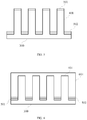
FIG. 3 shows a diagram of the first masking structures according to an embodiment of the present disclosure. -
FIG. 4 shows a diagram of the island structures according to an embodiment of the present disclosure. -
FIG. 5 shows a diagram of the layer of second masking structures and the first protection layer according to an embodiment of the present disclosure. -
FIG. 6 shows a diagram of the second protection layer according to an embodiment of the present disclosure. -
FIG. 7 shows a diagram of the second protection sub-layer according to an embodiment of the present disclosure. -
FIG. 8 shows a diagram of the substrate attached with a silicon-wafer sub-plate according to an embodiment of the present disclosure. -
FIG. 9 shows a diagram of the TFT substrate according to an embodiment of the present disclosure. - The disclosure will now be described in detail with reference to the accompanying drawings and examples.
- To solve the above mentioned problem, a technical scheme adopted by the present disclosure is to provide a method for manufacturing a TFT substrate. The method comprises: providing a silicon-wafer plate; forming first masking structures on the silicon-wafer plate and plasma etching to form island structures; cutting the island structures layer by layer to form a silicon-wafer sub-plate; attaching the silicon-wafer sub-plate on a substrate to form the TFT substrate. The method will be depicted in detail as follows.
- Referring to
FIG. 1, FIG. 1 is a flow chart of the method for manufacturing a TFT substrate according to an embodiment of the present disclosure. - S101: Providing a silicon-wafer plate.
- In this embodiment, in order to implement island elements on a flexible substrate, a silicon-wafer plate may be taken as material to prepare the island structures to be attached on the flexible substrate. Those skilled in the art should understand, materials having similar molecular structure as the silicon-wafer which may match the flexible substrate, such as the chemical elements in the same family of silicon, may also be utilized to prepare the island elements.
- S102: Forming first masking structures on the silicon-wafer plate and etching to form island structures.
- In this embodiment, a metal layer may be deposited as first masking structures on the silicon-wafer plate. Then the island structures may be formed by etching the silicon-wafer plate. The metal layer may be a layer of nickel.
- S103: Cutting the island structures layer by layer to form silicon-wafer sub-plates.
- In this embodiment, after the island structures are formed by etching the silicon-wafer plate, the island structures on the silicon-wafer plate may be cut layer by layer according to the structure and size of the island structures to be formed on the TFT substrate, so as to obtain silicon-wafer sub-plates as the island structures on the substrate.
- S104: Attaching the silicon-wafer sub-plate onto the substrate to form the TFT substrate.
- In this embodiment, the substrate may be a polyimide (PI) flexible substrate. The polyimide flexible substrate itself has a certain adhesive capacity. Accordingly, the silicon-wafer sub-plates may be attached onto the polyimide flexible substrate with the help of the adhesive capacity of the polyimide flexible substrate. In subsequence processes, the silicon-wafer sub-plate may be taken as the island structures matching TFT components in order to manufacture the TFT substrate.
- The present disclosure provides a method including forming first masking structures on a silicon-wafer substrate, etching the silicon-wafer substrate via the first masking structures to form island structures, cutting layer by layer the island structures and then attaching them onto a substrate to form the TFT substrate. Therefore, the implementation of the present disclosure may improve the stability of the substrate during bending and reduce the stress mismatch between the substrate and a TFT component film.
- Referring to
FIG. 2, FIG. 2 is a flow chart of the method for manufacturing a TFT substrate according to another embodiment of the present disclosure. - S201: Providing a silicon-wafer plate.
- In this embodiment, in order to implement island structures on a flexible substrate, a silicon-wafer plate may be taken as material to prepare the island structures attached on the flexible substrate. Those skilled in the art should understand, materials having similar molecular structure as the silicon-wafer which may match the flexible substrate, such as the chemical elements in the same family of silicon, may also be utilized to prepare the island structure.
- S202: forming first masking structures on the silicon-wafer plate and etching to form island structures.
- Referring to
FIG. 3-4 , in this embodiment, the silicon-wafer plate 300 may be coated with a layer of photoresist material. The photoresist material may be patterned by removing a portion of the photoresist material where thefirst masking structures 301 are to be set and keeping the remained photoresist material. Then a fist masking layer may be formed on a side of the silicon-wafer plate 300 which is coated with the photoresist material, wherein the first masking layer may cover the surface of the silicon-wafer plate and the photoresist material thereon. A portion of the first masking layer which covers the photoresist material may be removed with etching solution corresponding to the photoresist material while the left of the first masking layer which does not cover the photoresist material is kept. Thus thefirst masking structures 301 may be formed. By further plasma etching the silicon-wafer plate 300 and thefirst masking structures 301,island structures 401 may be formed. - In one embodiment, the photoresist material coating the silicon-
wafer plate 300 may be positive photoresist. A portion of the photoresist material on the silicon-wafer plate 300 where the first masking structures are to be set may be exposed to light. After applying developer, the photoresist material on the silicon-wafer plate 300 where thefirst masking structures 301 are to be set may be removed because the positive photoresist exposed to light will become liquid and washable by the etching solution. Apparently, the photoresist material coating the silicon-wafer plate 300 may alternatively be negative photoresist. All of the photoresist material on the silicon-wafer plate 300 except for the portion where thefirst masking structures 301 are to be set may be exposed to light. After applying developer, the photoresist material on the silicon-wafer plate 300 where thefirst masking structures 301 are to be set may be removed because only the negative photoresist exposed to light will become solid,. In this embodiment, if the photoresist material is negative photoresist, a portion of the photoresist material on the silicon-wafer plate 300 where thefirst masking structures 301 are to be set may not be exposed to light while the left is exposed to light and hardened. Thus, the photoresist material on the silicon-wafer plate 300 where thefirst masking structures 301 are to be set may be washed away by etching solution. - In one embodiment, the exposure time of the photoresist material on the surface of the silicon-
wafer plate 300 may be determined according to the height of the pattern to be formed. It should be noted that the exposure time should be long enough for removing the photoresist material on the surface of the silicon-wafer plate 300 at the location where thefirst masking structures 301 are to be set. - In one embodiment, a plasma beam may be shot towards the surface of the silicon-
wafer plate 300 and thefirst masking structures 301. The plasma hits the silicon-wafer plate 300 so that the requiredisland structures 401 may be formed. - In one embodiment, the
first masking structures 301 may include nickel or other metal. Apparently, those skilled in the art should understand that elements having similar chemical and physical characters as nickel, such as elements of the same family of nickel, may also be utilized as thefirst masking structures 301 of this embodiment. - In one embodiment, the thickness of the
first masking structures 301 may be 100 nm. Apparently, those skilled in the art should understand that the thickness of thefirst masking structures 301 should be thick enough for thefirst masking structures 301 to function as the etching mask during plasma etching of the silicon-wafer plate 300. - S203: Depositing a layer of second masking structures on the silicon-wafer plate and forming a first protection layer.
- Referring to
FIG. 5 , in this embodiment, a layer ofsecond masking structures 501 may be deposited on a surface of the silicon-wafer plate 300 where theisland structures 401 have been formed. Afirst protection layer 502 may be formed and then hardened on a portion of thesecond masking structures 501 which is not located on the island structures of the silicon-wafer plate 300. - In one embodiment, in order to harden the
first protection layer 502, thefirst protection layer 502 may be placed in a first temperature environment during a first predetermined time. By hardening thefirst protection layer 502 with a constant temperature, the adhesive force between thefirst protection layer 502 and thesecond masking structures 501 may be enhanced. The first temperature may be 180°C and the first predetermined time may be 1 min. Those skilled in the art should understand that the first temperature and the first predetermined time may be determined according to the thickness and area of thefirst protection layer 502, and intend to make thefirst protection layer 502 to have enough stiffness and enough adhesive force with the second masking structures. The above-mentioned values are just illustrative and should not be taken as limit to the scope of the present disclosure. - In one embodiment, the
first protection layer 502 may include polymethyl methacrylate (PMMA). The portion of thesecond masking structures 501 which is not located on theisland structures 401 of the silicon-wafer plate 300 may be coated with 100 nm of PMMA which may help to attach thesecond masking structures 501 to the silicon-wafer plate 300. PMMA should be thick enough to provide enough adhesive force between the layer ofsecond masking structures 501 and the silicon-wafer plate 300 and may be determined based on the size and thickness of the layer ofsecond masking structures 501. Those skilled in the art should understand that thefirst protection 502 may also include other adhesive colloid, and the thickness of the colloid may be determined based on the adhesion between the silicon-wafer plate 300 and the layer ofsecond masking structures 501, and the size and thickness of the layer ofsecond masking structures 501. - In one embodiment, the
second masking structures 501 may also be deposited on the surface of theisland structures 401. Thesecond masking structures 501 may be deposited on the surface of the silicon-wafer plate 300 by PVD (physical vapor deposition) such as vacuum plating, sputtering or ion plating. - In one embodiment, the layer of
second masking structures 501 may be a metal layer of gold. Thesecond masking structures 501 may be deposited on a portion of the silicon-wafer plate 300 where theisland structures 401 are not formed so as to facilitate the separation of the bottom of theisland structures 401 from thefirst protection layer 502. Apparently, those skilled in the art should understand that other metals which may facilitate the separation of the bottom of theisland structures 401 from thefirst protection layer 502 may also be utilized to form thesecond masking structures 501. - In one embodiment, the thickness of the layer of
second masking structures 501 may be 30 nm. Apparently, those skilled in the art may understand that the thickness of the layer ofsecond masking structures 501 should be large enough for facilitating the separation of the bottom of theisland structure 401 from thefirst protection layer 502. - S204: Removing the layer of second masking structures on the surface of the island structures and forming a second protection layer wrapping around the island structures.
- Referring to
FIG. 6 , in this embodiment, etching solution corresponding to thesecond masking structures 501 may be utilized to etch thesecond masking structures 501 on the surface of theisland structures 401. Thesecond masking structures 501 deposited on the portion of the silicon-wafer plate 300 where theisland structures 401 are not formed may not be etched by the etching solution since it is covered by thefirst protection layer 502. Consequently, only thesecond masking structures 501 deposited on the surface of theisland structures 401 far away from thefirst protection layer 502 will be etched. Then asecond protection layer 601 wrapping around theisland structure 401 may be formed and hardened on the silicon-wafer plate 300. - In one embodiment, in order to harden the
second protection layer 601, thesecond protection layer 601 may be placed in a second temperature environment during a second predetermined time. By hardening thesecond protection layer 601 with a constant temperature, the adhesive force between thesecond protection layer 601 and theisland structure 401 may be enhanced. The second temperature may be 80°C and the second predetermined time may be 4 h. Those skilled in the art should understand that the second temperature and the second predetermined time may be determined according to the thickness and area of thesecond protection layer 601, and intend to make thesecond protection layer 601 to have enough stiffness and adhesive force with theisland structures 401. The above-mentioned values are just illustrative and should not be taken as limit to the scope of the present disclosure. - S205: cutting layer by layer the island structures and the second protection layer to obtain second protection sub-layers.
- Referring to
FIG. 7 , in this embodiment, second protection sub-layers 700 may be obtained by cutting layer by layer theisland structures 401 and thesecond protection layer 601 wrapping around. The second protection sub-layers 700 wrap around a same number of silicon-wafer sub-plates as the island structures, which will be utilized in subsequent processes for manufacturing the TFT substrate. - In one embodiment, the
second protection layer 601 may include an epoxy layer. Thesecond protection layer 601 wrapping around the silicon-wafer sub-plates may be hardened to maintain the distance D of each two of the silicon-wafer sub-plates. Those skilled in the art should understand, the distance D may be determined according to the required distance between the island structures on the TFT substrate. - In one embodiment, the
island structures 401 and thesecond protection layer 601 wrapping around may be cut along a cutting direction parallel to the extending direction of the silicon-wafer plate 300. Apparently, those skilled in the art should understand, theisland structures 401 and thesecond protection layer 601 wrapping around may also be cut one by one so as to acquire the silicon-wafer sub-plates 701 for manufacturing the island elements on the TFT substrate. The thickness of thesecond protection layer 700 may be determined according to the required thickness of the island elements on the TFT substrate. - In one embodiment, a nanometer diamond cutter may be utilized to cut layer by layer the
island structures 401 and thesecond protection layer 601 wrapping around so as to obtain thesecond protection sub-layer 700. Apparently, those skilled in the art should understand that other nano-sized cutting tools such as laser may also be utilized. - S206: Attaching the second protection sub-layer onto the substrate and etching the second protection sub-layer to expose the silicon-wafer sub-plates so as to acquire the TFT substrate.
- Referring to
FIG. 8 , in this embodiment, the substrate may be a polyimide (PI) flexible substrate. The polyimide flexible substrate itself has a certain adhesive capacity. It should be understood that any substrate having a certain adhesive capacity may also be utilized to manufacturing theTFT substrate 801 of the present disclosure. - The
second protection sub-layer 700 obtained in the previous steps may be attached onto a substrate 801.The silicon-wafer sub-plates 701 may be exposed by plasma etching thesecond protection layer 700. After plasma etching, thesecond protection layer 601 on thesubstrate 801 may be removed, and the silicon-wafer sub-plates may be kept as the island elements of the TFT substrate. Then thesubstrate 801 may be placed in a third temperature environment during a third predetermined time so as to enhance the adhesive force between the silicon-wafer sub-plates 701 and thesubstrate 801. The silicon-wafer sub-plates 701 may be utilized as the island elements matching the TFT components for the sequent processes. - In one embodiment, the third temperature may be 150°C and the third predetermined time may be 3 min. Those skilled in the art should understand, the third temperature and the third predetermined time may be determined based on the thickness and area of the silicon-
wafer sub-plates 701 and the adhesion between the silicon-wafer sub-plates 701 and thesubstrate 801, and intend to provide enough adhesive force between the silicon-wafer sub-plates 701 and thesubstrate 801. The above-mentioned values are just illustrative and should not be taken as limit to the scope of the present disclosure. - In conclusion, according to the present disclosure, the island structures may be obtained by etching the silicon-wafer plate via the first masking structures, and the silicon-wafer sub-plates for manufacturing the island elements of the TFT substrate may be obtained by cutting layer by layer the island structures. The acquired silicon-wafer sub-plates may be attached onto the substrate to form the TFT substrate. Therefore, the present disclosure may improve the stability of the substrate during bending and reduce the stress mismatch between the substrate and the film of a TFT component.
- Referring to
FIG. 9, FIG. 9 shows a diagram of the TFT substrate according to an embodiment of the present disclosure. - In this embodiment, the
TFT substrate 900 may include aTFT component film 901 and thesubstrate 902. TheTFT substrate 900 may be manufactured by the method described in the above embodiments. Therefore, the stress mismatch during bending between theTFT component film 901 and thesubstrate 902 of theTFT substrate 900 may be reduced, and the stability of theTFT substrate 900 during bending may be improved. - The foregoing is merely embodiments of the present disclosure, and is not intended to limit the scope of the disclosure. Any transformation of equivalent structure or equivalent process which uses the specification and the accompanying drawings of the present disclosure, or directly or indirectly application in other related technical fields, are likewise included within the scope of the protection of the present disclosure.
Claims (17)
- A method for manufacturing a TFT substrate, comprising:providing a silicon-wafer plate;coating the silicon-wafer plate with a layer of photoresist material;patterning the photoresist material and removing a portion of the photoresist material where first masking structures are to be set;forming a first masking layer on a side of the silicon-wafer plate which is coated with the photoresist material, wherein the first masking layer covers the photoresist material;removing a portion of the first masking layer which covers the photoresist material with an etching solution corresponding to the photoresist material so as to form the first masking structures;plasma etching the silicon-wafer plate to form island structures;cutting the island structures layer by layer to form a silicon-wafer sub-plate; andattaching the silicon-wafer sub-plate onto a substrate to form the TFT substrate.
- The method of claim 1, after forming the island structures, further comprising:depositing a layer of second masking structures on the silicon-wafer plate;forming a first protection layer on a portion of the second masking structures of the silicon-wafer plate which are not on the island structures;hardening the first protection layer;removing other portions of the second masking structures located on the island structures and far away from the first protection layer with an etching solution corresponding to the layer of second masking structures;forming a second protection layer wrapping around the island structures on the silicon-wafer plate; andhardening the second protection layer.
- The method of claim 2, wherein
the step of hardening the first protection layer, comprises:placing the first protection layer in a first temperature environment during a first predetermined time, to harden the first protection layer;the step of hardening the second protection layer, comprises:
placing the second protection layer in a second temperature environment during a second predetermined time, to harden the second protection layer. - The method of claim 2, wherein the step of cutting the island structures layer by layer, comprises:
cutting layer by layer the island structures and the second protection layer to obtain a second protection sub-layer, wherein the second protection sub-layer has the silicon-wafer sub-plate wrapped therein. - The method of claim 4, wherein a direction for cutting layer by layer the second protection layer wrapping around the island structures is parallel to an extending direction of the silicon-wafer plate.
- The method of claim 4, further comprising:transferring the second protection sub-layer onto the substrate;plasma etching the second protection sub-layer to expose the silicon-wafer sub-plate, to form the TFT substrate.
- The method of claim 4, further comprising:
placing the TFT substrate in a third temperature environment during a third predetermined time. - A method for manufacturing a TFT substrate, comprising:providing a silicon-wafer plate;forming first masking structures on the silicon-wafer plate and etching to form island structures;cutting the island structures layer by layer to form a silicon-wafer sub-plate; andattaching the silicon-wafer sub-plate on a substrate to form the TFT substrate.
- The method of claim 8, wherein the step of forming first masking structures on the silicon-wafer plate, comprises:coating the silicon-wafer with a layer of photoresist material;patterning the photoresist material and removing a portion of the photoresist material where the first masking structures are to be set;forming a first masking layer on a side of the silicon-wafer plate which is coated with the photoresist material, wherein the first masking layer covers the photoresist material;removing portions of the first masking layer which cover the photoresist material with an etching solution corresponding to the photoresist material, so as to form the first masking structures.
- The method of claim 8, wherein the step of forming first masking structures on the silicon-wafer plate and etching comprises: plasma etching the silicon-wafer plate to form the island structures.
- The method of claim 8, after forming the island structures, further comprising:depositing a layer of second masking structures on the silicon-wafer plate;forming a first protection layer on a portion of the second masking structures of the silicon-wafer plate which are not on the island structures;hardening the first protection layer;removing other portions of the layer of second masking structures on a surface of the island structures far away from the first protection layer with an etching solution of the layer of second masking structures;forming on the silicon-wafer plate a second protection layer wrapping around the island structures; andhardening the second protection layer.
- The method of claim 11, wherein
the step of hardening the first protection layer comprises:placing the first protection layer in a first temperature environment during a first predetermined time to harden the first protection layer;the step of hardening the second protection layer comprises:
placing the second protection layer in a second temperature environment during a second predetermined time to harden the second protection layer. - The method of claim 11, wherein the step of the cutting the island structures layer by layer comprises:
cutting layer by layer the island structures and the second protection layer to obtain second protection sub-layer, wherein the second protection sub-layer has the silicon-wafer sub-plate wrapped inside. - The method of claim 13, wherein a direction for cutting layer by layer the second protection layer wrapping around the island structures is parallel to an extending direction of the silicon-wafer plate.
- The method of claim 13, further comprising:transferring the second protection sub-layer onto the substrate;plasma etching the second protection sub-layer to expose the silicon-wafer sub-plate, to form the TFT substrate.
- The method of claim 13, further comprising:
placing the TFT substrate in a third temperature environment during a third predetermined time. - A TFT substrate, manufactured by a manufacturing method, wherein the method comprises:providing a silicon-wafer plate;forming first masking structures on the silicon-wafer plate and etching to form island structures;cutting the island structures layer by layer to form a silicon-wafer sub-plate; andattaching the silicon-wafer sub-plate on a substrate to form the TFT substrate.
Applications Claiming Priority (2)
| Application Number | Priority Date | Filing Date | Title |
|---|---|---|---|
| CN201710976235.8A CN107845606B (en) | 2017-10-17 | 2017-10-17 | A kind of preparation method of TFT substrate and TFT substrate |
| PCT/CN2017/112507 WO2019075841A1 (en) | 2017-10-17 | 2017-11-23 | Manufacturing method of tft substrate and tft substrate |
Publications (3)
| Publication Number | Publication Date |
|---|---|
| EP3699954A1 true EP3699954A1 (en) | 2020-08-26 |
| EP3699954A4 EP3699954A4 (en) | 2021-07-14 |
| EP3699954B1 EP3699954B1 (en) | 2025-08-06 |
Family
ID=61662540
Family Applications (1)
| Application Number | Title | Priority Date | Filing Date |
|---|---|---|---|
| EP17929206.5A Active EP3699954B1 (en) | 2017-10-17 | 2017-11-23 | Manufacturing method of tft substrate and tft substrate |
Country Status (6)
| Country | Link |
|---|---|
| US (1) | US10930546B2 (en) |
| EP (1) | EP3699954B1 (en) |
| JP (1) | JP6994566B2 (en) |
| KR (1) | KR102307137B1 (en) |
| CN (1) | CN107845606B (en) |
| WO (1) | WO2019075841A1 (en) |
Family Cites Families (8)
| Publication number | Priority date | Publication date | Assignee | Title |
|---|---|---|---|---|
| TWI402935B (en) * | 2005-05-17 | 2013-07-21 | Koninkl Philips Electronics Nv | Color active matrix display |
| JP5271541B2 (en) * | 2006-01-16 | 2013-08-21 | パナソニック株式会社 | Semiconductor chip manufacturing method, field effect transistor and manufacturing method thereof |
| JP2009076729A (en) | 2007-09-21 | 2009-04-09 | Semiconductor Energy Lab Co Ltd | Method of manufacturing semiconductor device |
| CN102969320B (en) * | 2012-12-10 | 2015-10-21 | 京东方科技集团股份有限公司 | Flexible display substrates and preparation method thereof, flexible display apparatus |
| CN106158582B (en) * | 2015-04-01 | 2018-09-28 | 中国科学院上海高等研究院 | Neighbour's shadow effect auxiliary array method prepares layer and shifts thin crystal silicon technique |
| CN105355634B (en) * | 2015-11-20 | 2019-11-15 | 深圳市华星光电技术有限公司 | Thin film transistor array panel and manufacturing method thereof |
| CN105679800B (en) * | 2016-01-27 | 2019-08-13 | 京东方科技集团股份有限公司 | OLED display screen, manufacturing method thereof, and display device |
| CN105870265A (en) * | 2016-04-19 | 2016-08-17 | 京东方科技集团股份有限公司 | Light-emitting diode substrate and preparation method thereof and display device |
-
2017
- 2017-10-17 CN CN201710976235.8A patent/CN107845606B/en active Active
- 2017-11-23 KR KR1020207014093A patent/KR102307137B1/en active Active
- 2017-11-23 US US15/740,286 patent/US10930546B2/en active Active
- 2017-11-23 EP EP17929206.5A patent/EP3699954B1/en active Active
- 2017-11-23 JP JP2020518621A patent/JP6994566B2/en active Active
- 2017-11-23 WO PCT/CN2017/112507 patent/WO2019075841A1/en not_active Ceased
Also Published As
| Publication number | Publication date |
|---|---|
| CN107845606B (en) | 2020-05-05 |
| KR20200065073A (en) | 2020-06-08 |
| JP6994566B2 (en) | 2022-01-14 |
| US20190385900A1 (en) | 2019-12-19 |
| EP3699954A4 (en) | 2021-07-14 |
| EP3699954B1 (en) | 2025-08-06 |
| CN107845606A (en) | 2018-03-27 |
| WO2019075841A1 (en) | 2019-04-25 |
| JP2020536383A (en) | 2020-12-10 |
| KR102307137B1 (en) | 2021-09-30 |
| US10930546B2 (en) | 2021-02-23 |
Similar Documents
| Publication | Publication Date | Title |
|---|---|---|
| US9633899B2 (en) | Method for patterning a graphene layer and method for manufacturing a display substrate | |
| CN111524957B (en) | Display substrate and manufacturing method thereof, display device | |
| WO2015096416A1 (en) | Thin-film transistor and manufacturing method therefor, array substrate and manufacturing method therefor | |
| US20090061560A1 (en) | Method of fabricating organic electronic device | |
| JP4306540B2 (en) | Thin processing method of semiconductor substrate | |
| CN108470849B (en) | Flexible substrate and manufacturing method thereof | |
| US11257955B2 (en) | Thin film transistor, array substrate, and method for fabricating the same | |
| EP2709159A1 (en) | Fabricating method of thin film transistor, fabricating method of array substrate and display device | |
| CN103700670B (en) | Array base palte and preparation method thereof, display device | |
| KR20060019976A (en) | Manufacturing method of organic thin film transistor and liquid crystal display device | |
| CN107164788B (en) | Mask plate and manufacturing method thereof | |
| WO2012046428A1 (en) | Method for producing semiconductor device | |
| CN106847704A (en) | Method, thin film transistor (TFT) and preparation method to layer on surface of metal roughening treatment | |
| CN103489874B (en) | Array base palte and preparation method thereof, display unit | |
| WO2017152552A1 (en) | Thin film transistor and method for manufacturing same, array substrate and method for manufacturing same, and display device | |
| US20130043474A1 (en) | Active array substrate and method for manufacturing the same | |
| CN100563022C (en) | Organic thin film transistor array substrate and manufacturing method thereof | |
| KR100767903B1 (en) | Method for producing the same, deposition method, electronic device, and electronic apparatus | |
| CN104409361A (en) | Thin-film transistor, preparation method of thin-film transistor, array substrate and display device | |
| CN108376749B (en) | A packaging method for a display panel, a display panel and a display device | |
| CN106876254A (en) | The preparation method of array base palte, display device, thin film transistor (TFT) and film layer figure | |
| US10930546B2 (en) | TFT substrate and method for manufacturing the same | |
| GB2542094B (en) | Method for manufacturing coplanar oxide semiconductor TFT substrate | |
| CN108365129B (en) | Display panel, manufacturing method thereof and display device | |
| US9484552B2 (en) | Manufacturing method of flexible device substrate |
Legal Events
| Date | Code | Title | Description |
|---|---|---|---|
| STAA | Information on the status of an ep patent application or granted ep patent |
Free format text: STATUS: THE INTERNATIONAL PUBLICATION HAS BEEN MADE |
|
| PUAI | Public reference made under article 153(3) epc to a published international application that has entered the european phase |
Free format text: ORIGINAL CODE: 0009012 |
|
| STAA | Information on the status of an ep patent application or granted ep patent |
Free format text: STATUS: REQUEST FOR EXAMINATION WAS MADE |
|
| 17P | Request for examination filed |
Effective date: 20200423 |
|
| AK | Designated contracting states |
Kind code of ref document: A1 Designated state(s): AL AT BE BG CH CY CZ DE DK EE ES FI FR GB GR HR HU IE IS IT LI LT LU LV MC MK MT NL NO PL PT RO RS SE SI SK SM TR |
|
| AX | Request for extension of the european patent |
Extension state: BA ME |
|
| DAV | Request for validation of the european patent (deleted) | ||
| DAX | Request for extension of the european patent (deleted) | ||
| A4 | Supplementary search report drawn up and despatched |
Effective date: 20210614 |
|
| RIC1 | Information provided on ipc code assigned before grant |
Ipc: H01L 21/77 20170101AFI20210607BHEP Ipc: H01L 27/12 20060101ALI20210607BHEP |
|
| REG | Reference to a national code |
Ref country code: DE Ref legal event code: R079 Free format text: PREVIOUS MAIN CLASS: H01L0021770000 Ipc: H10D0086000000 Ref document number: 602017091108 Country of ref document: DE |
|
| RIC1 | Information provided on ipc code assigned before grant |
Ipc: H10D 86/00 20250101AFI20250131BHEP |
|
| GRAP | Despatch of communication of intention to grant a patent |
Free format text: ORIGINAL CODE: EPIDOSNIGR1 |
|
| STAA | Information on the status of an ep patent application or granted ep patent |
Free format text: STATUS: GRANT OF PATENT IS INTENDED |
|
| INTG | Intention to grant announced |
Effective date: 20250417 |
|
| GRAS | Grant fee paid |
Free format text: ORIGINAL CODE: EPIDOSNIGR3 |
|
| GRAA | (expected) grant |
Free format text: ORIGINAL CODE: 0009210 |
|
| STAA | Information on the status of an ep patent application or granted ep patent |
Free format text: STATUS: THE PATENT HAS BEEN GRANTED |
|
| P01 | Opt-out of the competence of the unified patent court (upc) registered |
Free format text: CASE NUMBER: APP_30193/2025 Effective date: 20250624 |
|
| AK | Designated contracting states |
Kind code of ref document: B1 Designated state(s): AL AT BE BG CH CY CZ DE DK EE ES FI FR GB GR HR HU IE IS IT LI LT LU LV MC MK MT NL NO PL PT RO RS SE SI SK SM TR |
|
| REG | Reference to a national code |
Ref country code: GB Ref legal event code: FG4D |
|
| REG | Reference to a national code |
Ref country code: CH Ref legal event code: EP |
|
| REG | Reference to a national code |
Ref country code: DE Ref legal event code: R096 Ref document number: 602017091108 Country of ref document: DE |
|
| REG | Reference to a national code |
Ref country code: IE Ref legal event code: FG4D |
|
| REG | Reference to a national code |
Ref country code: NL Ref legal event code: MP Effective date: 20250806 |
|
| PG25 | Lapsed in a contracting state [announced via postgrant information from national office to epo] |
Ref country code: IS Free format text: LAPSE BECAUSE OF FAILURE TO SUBMIT A TRANSLATION OF THE DESCRIPTION OR TO PAY THE FEE WITHIN THE PRESCRIBED TIME-LIMIT Effective date: 20251206 |
|
| PGFP | Annual fee paid to national office [announced via postgrant information from national office to epo] |
Ref country code: DE Payment date: 20251119 Year of fee payment: 9 |
|
| PG25 | Lapsed in a contracting state [announced via postgrant information from national office to epo] |
Ref country code: NO Free format text: LAPSE BECAUSE OF FAILURE TO SUBMIT A TRANSLATION OF THE DESCRIPTION OR TO PAY THE FEE WITHIN THE PRESCRIBED TIME-LIMIT Effective date: 20251106 |
|
| REG | Reference to a national code |
Ref country code: LT Ref legal event code: MG9D |
|
| PG25 | Lapsed in a contracting state [announced via postgrant information from national office to epo] |
Ref country code: PT Free format text: LAPSE BECAUSE OF FAILURE TO SUBMIT A TRANSLATION OF THE DESCRIPTION OR TO PAY THE FEE WITHIN THE PRESCRIBED TIME-LIMIT Effective date: 20251209 |
|
| PG25 | Lapsed in a contracting state [announced via postgrant information from national office to epo] |
Ref country code: FI Free format text: LAPSE BECAUSE OF FAILURE TO SUBMIT A TRANSLATION OF THE DESCRIPTION OR TO PAY THE FEE WITHIN THE PRESCRIBED TIME-LIMIT Effective date: 20250806 |
|
| PG25 | Lapsed in a contracting state [announced via postgrant information from national office to epo] |
Ref country code: HR Free format text: LAPSE BECAUSE OF FAILURE TO SUBMIT A TRANSLATION OF THE DESCRIPTION OR TO PAY THE FEE WITHIN THE PRESCRIBED TIME-LIMIT Effective date: 20250806 Ref country code: NL Free format text: LAPSE BECAUSE OF FAILURE TO SUBMIT A TRANSLATION OF THE DESCRIPTION OR TO PAY THE FEE WITHIN THE PRESCRIBED TIME-LIMIT Effective date: 20250806 |
|
| PG25 | Lapsed in a contracting state [announced via postgrant information from national office to epo] |
Ref country code: GR Free format text: LAPSE BECAUSE OF FAILURE TO SUBMIT A TRANSLATION OF THE DESCRIPTION OR TO PAY THE FEE WITHIN THE PRESCRIBED TIME-LIMIT Effective date: 20251107 |
|
| PG25 | Lapsed in a contracting state [announced via postgrant information from national office to epo] |
Ref country code: SE Free format text: LAPSE BECAUSE OF FAILURE TO SUBMIT A TRANSLATION OF THE DESCRIPTION OR TO PAY THE FEE WITHIN THE PRESCRIBED TIME-LIMIT Effective date: 20250806 |
|
| PG25 | Lapsed in a contracting state [announced via postgrant information from national office to epo] |
Ref country code: LV Free format text: LAPSE BECAUSE OF FAILURE TO SUBMIT A TRANSLATION OF THE DESCRIPTION OR TO PAY THE FEE WITHIN THE PRESCRIBED TIME-LIMIT Effective date: 20250806 |
|
| PG25 | Lapsed in a contracting state [announced via postgrant information from national office to epo] |
Ref country code: BG Free format text: LAPSE BECAUSE OF FAILURE TO SUBMIT A TRANSLATION OF THE DESCRIPTION OR TO PAY THE FEE WITHIN THE PRESCRIBED TIME-LIMIT Effective date: 20250806 Ref country code: PL Free format text: LAPSE BECAUSE OF FAILURE TO SUBMIT A TRANSLATION OF THE DESCRIPTION OR TO PAY THE FEE WITHIN THE PRESCRIBED TIME-LIMIT Effective date: 20250806 |
|
| PG25 | Lapsed in a contracting state [announced via postgrant information from national office to epo] |
Ref country code: RS Free format text: LAPSE BECAUSE OF FAILURE TO SUBMIT A TRANSLATION OF THE DESCRIPTION OR TO PAY THE FEE WITHIN THE PRESCRIBED TIME-LIMIT Effective date: 20251106 |
|
| PG25 | Lapsed in a contracting state [announced via postgrant information from national office to epo] |
Ref country code: ES Free format text: LAPSE BECAUSE OF FAILURE TO SUBMIT A TRANSLATION OF THE DESCRIPTION OR TO PAY THE FEE WITHIN THE PRESCRIBED TIME-LIMIT Effective date: 20250806 |
|
| REG | Reference to a national code |
Ref country code: AT Ref legal event code: MK05 Ref document number: 1823552 Country of ref document: AT Kind code of ref document: T Effective date: 20250806 |
|
| PG25 | Lapsed in a contracting state [announced via postgrant information from national office to epo] |
Ref country code: RO Free format text: LAPSE BECAUSE OF FAILURE TO SUBMIT A TRANSLATION OF THE DESCRIPTION OR TO PAY THE FEE WITHIN THE PRESCRIBED TIME-LIMIT Effective date: 20250806 |
|
| PG25 | Lapsed in a contracting state [announced via postgrant information from national office to epo] |
Ref country code: SM Free format text: LAPSE BECAUSE OF FAILURE TO SUBMIT A TRANSLATION OF THE DESCRIPTION OR TO PAY THE FEE WITHIN THE PRESCRIBED TIME-LIMIT Effective date: 20250806 |
|
| PG25 | Lapsed in a contracting state [announced via postgrant information from national office to epo] |
Ref country code: DK Free format text: LAPSE BECAUSE OF FAILURE TO SUBMIT A TRANSLATION OF THE DESCRIPTION OR TO PAY THE FEE WITHIN THE PRESCRIBED TIME-LIMIT Effective date: 20250806 |
|
| PG25 | Lapsed in a contracting state [announced via postgrant information from national office to epo] |
Ref country code: AT Free format text: LAPSE BECAUSE OF FAILURE TO SUBMIT A TRANSLATION OF THE DESCRIPTION OR TO PAY THE FEE WITHIN THE PRESCRIBED TIME-LIMIT Effective date: 20250806 |
|
| PG25 | Lapsed in a contracting state [announced via postgrant information from national office to epo] |
Ref country code: IT Free format text: LAPSE BECAUSE OF FAILURE TO SUBMIT A TRANSLATION OF THE DESCRIPTION OR TO PAY THE FEE WITHIN THE PRESCRIBED TIME-LIMIT Effective date: 20250806 |
|
| PG25 | Lapsed in a contracting state [announced via postgrant information from national office to epo] |
Ref country code: CZ Free format text: LAPSE BECAUSE OF FAILURE TO SUBMIT A TRANSLATION OF THE DESCRIPTION OR TO PAY THE FEE WITHIN THE PRESCRIBED TIME-LIMIT Effective date: 20250806 |
|
| PG25 | Lapsed in a contracting state [announced via postgrant information from national office to epo] |
Ref country code: EE Free format text: LAPSE BECAUSE OF FAILURE TO SUBMIT A TRANSLATION OF THE DESCRIPTION OR TO PAY THE FEE WITHIN THE PRESCRIBED TIME-LIMIT Effective date: 20250806 Ref country code: SK Free format text: LAPSE BECAUSE OF FAILURE TO SUBMIT A TRANSLATION OF THE DESCRIPTION OR TO PAY THE FEE WITHIN THE PRESCRIBED TIME-LIMIT Effective date: 20250806 |