EP3699932A1 - Insulating film, insulated conductor, metal base substrate - Google Patents
Insulating film, insulated conductor, metal base substrate Download PDFInfo
- Publication number
- EP3699932A1 EP3699932A1 EP19747896.9A EP19747896A EP3699932A1 EP 3699932 A1 EP3699932 A1 EP 3699932A1 EP 19747896 A EP19747896 A EP 19747896A EP 3699932 A1 EP3699932 A1 EP 3699932A1
- Authority
- EP
- European Patent Office
- Prior art keywords
- insulating film
- single crystal
- particles
- resin
- volume
- Prior art date
- Legal status (The legal status is an assumption and is not a legal conclusion. Google has not performed a legal analysis and makes no representation as to the accuracy of the status listed.)
- Withdrawn
Links
- 239000000758 substrate Substances 0.000 title claims abstract description 66
- 229910052751 metal Inorganic materials 0.000 title claims abstract description 58
- 239000002184 metal Substances 0.000 title claims abstract description 58
- 239000004020 conductor Substances 0.000 title claims abstract description 40
- 239000002245 particle Substances 0.000 claims abstract description 103
- PNEYBMLMFCGWSK-UHFFFAOYSA-N Alumina Chemical compound [O-2].[O-2].[O-2].[Al+3].[Al+3] PNEYBMLMFCGWSK-UHFFFAOYSA-N 0.000 claims abstract description 65
- 239000013078 crystal Substances 0.000 claims abstract description 54
- 229920005989 resin Polymers 0.000 claims abstract description 48
- 239000011347 resin Substances 0.000 claims abstract description 48
- 239000004962 Polyamide-imide Substances 0.000 claims abstract description 27
- 229920002312 polyamide-imide Polymers 0.000 claims abstract description 27
- 239000011888 foil Substances 0.000 claims abstract description 19
- 229920001721 polyimide Polymers 0.000 claims abstract description 19
- 239000004642 Polyimide Substances 0.000 claims abstract description 18
- 239000000203 mixture Substances 0.000 claims abstract description 11
- RYGMFSIKBFXOCR-UHFFFAOYSA-N Copper Chemical compound [Cu] RYGMFSIKBFXOCR-UHFFFAOYSA-N 0.000 description 37
- 239000000919 ceramic Substances 0.000 description 35
- 239000000243 solution Substances 0.000 description 33
- 229910052802 copper Inorganic materials 0.000 description 28
- 239000010949 copper Substances 0.000 description 28
- SECXISVLQFMRJM-UHFFFAOYSA-N N-Methylpyrrolidone Chemical compound CN1CCCC1=O SECXISVLQFMRJM-UHFFFAOYSA-N 0.000 description 22
- 238000004070 electrodeposition Methods 0.000 description 18
- 238000010438 heat treatment Methods 0.000 description 18
- 238000000034 method Methods 0.000 description 17
- 230000000052 comparative effect Effects 0.000 description 16
- 239000012790 adhesive layer Substances 0.000 description 15
- 239000010410 layer Substances 0.000 description 15
- 229920002050 silicone resin Polymers 0.000 description 15
- 238000000576 coating method Methods 0.000 description 13
- 238000004519 manufacturing process Methods 0.000 description 13
- 229920005575 poly(amic acid) Polymers 0.000 description 10
- 239000006185 dispersion Substances 0.000 description 9
- 239000003822 epoxy resin Substances 0.000 description 9
- 239000011256 inorganic filler Substances 0.000 description 9
- 229910003475 inorganic filler Inorganic materials 0.000 description 9
- 239000002105 nanoparticle Substances 0.000 description 9
- 229920000647 polyepoxide Polymers 0.000 description 9
- 239000000126 substance Substances 0.000 description 9
- VYPSYNLAJGMNEJ-UHFFFAOYSA-N Silicium dioxide Chemical compound O=[Si]=O VYPSYNLAJGMNEJ-UHFFFAOYSA-N 0.000 description 6
- 238000001035 drying Methods 0.000 description 6
- 239000010935 stainless steel Substances 0.000 description 5
- 229910001220 stainless steel Inorganic materials 0.000 description 5
- ARXJGSRGQADJSQ-UHFFFAOYSA-N 1-methoxypropan-2-ol Chemical compound COCC(C)O ARXJGSRGQADJSQ-UHFFFAOYSA-N 0.000 description 4
- 229910052582 BN Inorganic materials 0.000 description 4
- PZNSFCLAULLKQX-UHFFFAOYSA-N Boron nitride Chemical compound N#B PZNSFCLAULLKQX-UHFFFAOYSA-N 0.000 description 4
- 239000011248 coating agent Substances 0.000 description 4
- 239000010954 inorganic particle Substances 0.000 description 4
- 239000000463 material Substances 0.000 description 4
- 239000011859 microparticle Substances 0.000 description 4
- 238000002360 preparation method Methods 0.000 description 4
- 230000001681 protective effect Effects 0.000 description 4
- 239000002904 solvent Substances 0.000 description 4
- 229910052782 aluminium Inorganic materials 0.000 description 3
- XAGFODPZIPBFFR-UHFFFAOYSA-N aluminium Chemical compound [Al] XAGFODPZIPBFFR-UHFFFAOYSA-N 0.000 description 3
- 239000011889 copper foil Substances 0.000 description 3
- 230000003247 decreasing effect Effects 0.000 description 3
- 239000011342 resin composition Substances 0.000 description 3
- 238000003756 stirring Methods 0.000 description 3
- HLBLWEWZXPIGSM-UHFFFAOYSA-N 4-Aminophenyl ether Chemical compound C1=CC(N)=CC=C1OC1=CC=C(N)C=C1 HLBLWEWZXPIGSM-UHFFFAOYSA-N 0.000 description 2
- 239000012298 atmosphere Substances 0.000 description 2
- 230000007423 decrease Effects 0.000 description 2
- 230000000694 effects Effects 0.000 description 2
- 239000010419 fine particle Substances 0.000 description 2
- LNEPOXFFQSENCJ-UHFFFAOYSA-N haloperidol Chemical compound C1CC(O)(C=2C=CC(Cl)=CC=2)CCN1CCCC(=O)C1=CC=C(F)C=C1 LNEPOXFFQSENCJ-UHFFFAOYSA-N 0.000 description 2
- 239000011810 insulating material Substances 0.000 description 2
- 238000010030 laminating Methods 0.000 description 2
- 239000011259 mixed solution Substances 0.000 description 2
- 239000002243 precursor Substances 0.000 description 2
- 238000009210 therapy by ultrasound Methods 0.000 description 2
- XLYOFNOQVPJJNP-UHFFFAOYSA-N water Substances O XLYOFNOQVPJJNP-UHFFFAOYSA-N 0.000 description 2
- 229910000838 Al alloy Inorganic materials 0.000 description 1
- OKTJSMMVPCPJKN-UHFFFAOYSA-N Carbon Chemical compound [C] OKTJSMMVPCPJKN-UHFFFAOYSA-N 0.000 description 1
- 241000284156 Clerodendrum quadriloculare Species 0.000 description 1
- 229910000881 Cu alloy Inorganic materials 0.000 description 1
- GWEVSGVZZGPLCZ-UHFFFAOYSA-N Titan oxide Chemical compound O=[Ti]=O GWEVSGVZZGPLCZ-UHFFFAOYSA-N 0.000 description 1
- 238000002441 X-ray diffraction Methods 0.000 description 1
- GTDPSWPPOUPBNX-UHFFFAOYSA-N ac1mqpva Chemical compound CC12C(=O)OC(=O)C1(C)C1(C)C2(C)C(=O)OC1=O GTDPSWPPOUPBNX-UHFFFAOYSA-N 0.000 description 1
- 239000004844 aliphatic epoxy resin Substances 0.000 description 1
- 238000007611 bar coating method Methods 0.000 description 1
- 239000004841 bisphenol A epoxy resin Substances 0.000 description 1
- 239000004842 bisphenol F epoxy resin Substances 0.000 description 1
- 229910052799 carbon Inorganic materials 0.000 description 1
- 230000015556 catabolic process Effects 0.000 description 1
- PMHQVHHXPFUNSP-UHFFFAOYSA-M copper(1+);methylsulfanylmethane;bromide Chemical compound Br[Cu].CSC PMHQVHHXPFUNSP-UHFFFAOYSA-M 0.000 description 1
- 230000001186 cumulative effect Effects 0.000 description 1
- 210000003298 dental enamel Anatomy 0.000 description 1
- 238000007607 die coating method Methods 0.000 description 1
- 238000003618 dip coating Methods 0.000 description 1
- 239000002270 dispersing agent Substances 0.000 description 1
- 238000009826 distribution Methods 0.000 description 1
- 238000004870 electrical engineering Methods 0.000 description 1
- 238000011156 evaluation Methods 0.000 description 1
- 239000000835 fiber Substances 0.000 description 1
- 239000004845 glycidylamine epoxy resin Substances 0.000 description 1
- PCHJSUWPFVWCPO-UHFFFAOYSA-N gold Chemical compound [Au] PCHJSUWPFVWCPO-UHFFFAOYSA-N 0.000 description 1
- 229910052737 gold Inorganic materials 0.000 description 1
- 239000010931 gold Substances 0.000 description 1
- 238000007756 gravure coating Methods 0.000 description 1
- 230000017525 heat dissipation Effects 0.000 description 1
- 238000002347 injection Methods 0.000 description 1
- 239000007924 injection Substances 0.000 description 1
- 230000010354 integration Effects 0.000 description 1
- 239000007788 liquid Substances 0.000 description 1
- 239000012046 mixed solvent Substances 0.000 description 1
- 239000012299 nitrogen atmosphere Substances 0.000 description 1
- 229920003986 novolac Polymers 0.000 description 1
- SBOJXQVPLKSXOG-UHFFFAOYSA-N o-amino-hydroxylamine Chemical compound NON SBOJXQVPLKSXOG-UHFFFAOYSA-N 0.000 description 1
- 125000000962 organic group Chemical group 0.000 description 1
- 239000009719 polyimide resin Substances 0.000 description 1
- 238000003825 pressing Methods 0.000 description 1
- 239000011164 primary particle Substances 0.000 description 1
- 229910052594 sapphire Inorganic materials 0.000 description 1
- 239000004065 semiconductor Substances 0.000 description 1
- 239000000377 silicon dioxide Substances 0.000 description 1
- 229910000679 solder Inorganic materials 0.000 description 1
- 238000004528 spin coating Methods 0.000 description 1
- 238000010345 tape casting Methods 0.000 description 1
- 125000006158 tetracarboxylic acid group Chemical group 0.000 description 1
- OGIDPMRJRNCKJF-UHFFFAOYSA-N titanium oxide Inorganic materials [Ti]=O OGIDPMRJRNCKJF-UHFFFAOYSA-N 0.000 description 1
- 238000001132 ultrasonic dispersion Methods 0.000 description 1
Images

Classifications
-
- H—ELECTRICITY
- H01—ELECTRIC ELEMENTS
- H01B—CABLES; CONDUCTORS; INSULATORS; SELECTION OF MATERIALS FOR THEIR CONDUCTIVE, INSULATING OR DIELECTRIC PROPERTIES
- H01B3/00—Insulators or insulating bodies characterised by the insulating materials; Selection of materials for their insulating or dielectric properties
- H01B3/18—Insulators or insulating bodies characterised by the insulating materials; Selection of materials for their insulating or dielectric properties mainly consisting of organic substances
- H01B3/30—Insulators or insulating bodies characterised by the insulating materials; Selection of materials for their insulating or dielectric properties mainly consisting of organic substances plastics; resins; waxes
- H01B3/303—Macromolecular compounds obtained by reactions forming a linkage containing nitrogen with or without oxygen or carbon in the main chain of the macromolecule, not provided for in groups H01B3/38 or H01B3/302
- H01B3/306—Polyimides or polyesterimides
-
- H—ELECTRICITY
- H01—ELECTRIC ELEMENTS
- H01B—CABLES; CONDUCTORS; INSULATORS; SELECTION OF MATERIALS FOR THEIR CONDUCTIVE, INSULATING OR DIELECTRIC PROPERTIES
- H01B17/00—Insulators or insulating bodies characterised by their form
- H01B17/56—Insulating bodies
- H01B17/62—Insulating-layers or insulating-films on metal bodies
-
- C—CHEMISTRY; METALLURGY
- C08—ORGANIC MACROMOLECULAR COMPOUNDS; THEIR PREPARATION OR CHEMICAL WORKING-UP; COMPOSITIONS BASED THEREON
- C08G—MACROMOLECULAR COMPOUNDS OBTAINED OTHERWISE THAN BY REACTIONS ONLY INVOLVING UNSATURATED CARBON-TO-CARBON BONDS
- C08G73/00—Macromolecular compounds obtained by reactions forming a linkage containing nitrogen with or without oxygen or carbon in the main chain of the macromolecule, not provided for in groups C08G12/00 - C08G71/00
- C08G73/06—Polycondensates having nitrogen-containing heterocyclic rings in the main chain of the macromolecule
- C08G73/10—Polyimides; Polyester-imides; Polyamide-imides; Polyamide acids or similar polyimide precursors
- C08G73/1046—Polyimides containing oxygen in the form of ether bonds in the main chain
-
- C—CHEMISTRY; METALLURGY
- C08—ORGANIC MACROMOLECULAR COMPOUNDS; THEIR PREPARATION OR CHEMICAL WORKING-UP; COMPOSITIONS BASED THEREON
- C08G—MACROMOLECULAR COMPOUNDS OBTAINED OTHERWISE THAN BY REACTIONS ONLY INVOLVING UNSATURATED CARBON-TO-CARBON BONDS
- C08G73/00—Macromolecular compounds obtained by reactions forming a linkage containing nitrogen with or without oxygen or carbon in the main chain of the macromolecule, not provided for in groups C08G12/00 - C08G71/00
- C08G73/06—Polycondensates having nitrogen-containing heterocyclic rings in the main chain of the macromolecule
- C08G73/10—Polyimides; Polyester-imides; Polyamide-imides; Polyamide acids or similar polyimide precursors
- C08G73/14—Polyamide-imides
-
- C—CHEMISTRY; METALLURGY
- C08—ORGANIC MACROMOLECULAR COMPOUNDS; THEIR PREPARATION OR CHEMICAL WORKING-UP; COMPOSITIONS BASED THEREON
- C08J—WORKING-UP; GENERAL PROCESSES OF COMPOUNDING; AFTER-TREATMENT NOT COVERED BY SUBCLASSES C08B, C08C, C08F, C08G or C08H
- C08J5/00—Manufacture of articles or shaped materials containing macromolecular substances
- C08J5/18—Manufacture of films or sheets
-
- C—CHEMISTRY; METALLURGY
- C08—ORGANIC MACROMOLECULAR COMPOUNDS; THEIR PREPARATION OR CHEMICAL WORKING-UP; COMPOSITIONS BASED THEREON
- C08K—Use of inorganic or non-macromolecular organic substances as compounding ingredients
- C08K3/00—Use of inorganic substances as compounding ingredients
- C08K3/18—Oxygen-containing compounds, e.g. metal carbonyls
- C08K3/20—Oxides; Hydroxides
- C08K3/22—Oxides; Hydroxides of metals
-
- C—CHEMISTRY; METALLURGY
- C08—ORGANIC MACROMOLECULAR COMPOUNDS; THEIR PREPARATION OR CHEMICAL WORKING-UP; COMPOSITIONS BASED THEREON
- C08L—COMPOSITIONS OF MACROMOLECULAR COMPOUNDS
- C08L79/00—Compositions of macromolecular compounds obtained by reactions forming in the main chain of the macromolecule a linkage containing nitrogen with or without oxygen or carbon only, not provided for in groups C08L61/00 - C08L77/00
- C08L79/04—Polycondensates having nitrogen-containing heterocyclic rings in the main chain; Polyhydrazides; Polyamide acids or similar polyimide precursors
- C08L79/08—Polyimides; Polyester-imides; Polyamide-imides; Polyamide acids or similar polyimide precursors
-
- H—ELECTRICITY
- H01—ELECTRIC ELEMENTS
- H01B—CABLES; CONDUCTORS; INSULATORS; SELECTION OF MATERIALS FOR THEIR CONDUCTIVE, INSULATING OR DIELECTRIC PROPERTIES
- H01B17/00—Insulators or insulating bodies characterised by their form
- H01B17/56—Insulating bodies
- H01B17/66—Joining insulating bodies together, e.g. by bonding
-
- H—ELECTRICITY
- H01—ELECTRIC ELEMENTS
- H01B—CABLES; CONDUCTORS; INSULATORS; SELECTION OF MATERIALS FOR THEIR CONDUCTIVE, INSULATING OR DIELECTRIC PROPERTIES
- H01B3/00—Insulators or insulating bodies characterised by the insulating materials; Selection of materials for their insulating or dielectric properties
- H01B3/002—Inhomogeneous material in general
- H01B3/006—Other inhomogeneous material
-
- H—ELECTRICITY
- H01—ELECTRIC ELEMENTS
- H01B—CABLES; CONDUCTORS; INSULATORS; SELECTION OF MATERIALS FOR THEIR CONDUCTIVE, INSULATING OR DIELECTRIC PROPERTIES
- H01B7/00—Insulated conductors or cables characterised by their form
- H01B7/02—Disposition of insulation
-
- H—ELECTRICITY
- H05—ELECTRIC TECHNIQUES NOT OTHERWISE PROVIDED FOR
- H05K—PRINTED CIRCUITS; CASINGS OR CONSTRUCTIONAL DETAILS OF ELECTRIC APPARATUS; MANUFACTURE OF ASSEMBLAGES OF ELECTRICAL COMPONENTS
- H05K1/00—Printed circuits
- H05K1/02—Details
- H05K1/03—Use of materials for the substrate
- H05K1/05—Insulated conductive substrates, e.g. insulated metal substrate
-
- H—ELECTRICITY
- H05—ELECTRIC TECHNIQUES NOT OTHERWISE PROVIDED FOR
- H05K—PRINTED CIRCUITS; CASINGS OR CONSTRUCTIONAL DETAILS OF ELECTRIC APPARATUS; MANUFACTURE OF ASSEMBLAGES OF ELECTRICAL COMPONENTS
- H05K1/00—Printed circuits
- H05K1/02—Details
- H05K1/03—Use of materials for the substrate
- H05K1/05—Insulated conductive substrates, e.g. insulated metal substrate
- H05K1/056—Insulated conductive substrates, e.g. insulated metal substrate the metal substrate being covered by an organic insulating layer
-
- C—CHEMISTRY; METALLURGY
- C08—ORGANIC MACROMOLECULAR COMPOUNDS; THEIR PREPARATION OR CHEMICAL WORKING-UP; COMPOSITIONS BASED THEREON
- C08J—WORKING-UP; GENERAL PROCESSES OF COMPOUNDING; AFTER-TREATMENT NOT COVERED BY SUBCLASSES C08B, C08C, C08F, C08G or C08H
- C08J2379/00—Characterised by the use of macromolecular compounds obtained by reactions forming in the main chain of the macromolecule a linkage containing nitrogen with or without oxygen, or carbon only, not provided for in groups C08J2361/00 - C08J2377/00
- C08J2379/04—Polycondensates having nitrogen-containing heterocyclic rings in the main chain; Polyhydrazides; Polyamide acids or similar polyimide precursors
- C08J2379/08—Polyimides; Polyester-imides; Polyamide-imides; Polyamide acids or similar polyimide precursors
-
- C—CHEMISTRY; METALLURGY
- C08—ORGANIC MACROMOLECULAR COMPOUNDS; THEIR PREPARATION OR CHEMICAL WORKING-UP; COMPOSITIONS BASED THEREON
- C08K—Use of inorganic or non-macromolecular organic substances as compounding ingredients
- C08K3/00—Use of inorganic substances as compounding ingredients
- C08K3/18—Oxygen-containing compounds, e.g. metal carbonyls
- C08K3/20—Oxides; Hydroxides
- C08K3/22—Oxides; Hydroxides of metals
- C08K2003/2227—Oxides; Hydroxides of metals of aluminium
-
- C—CHEMISTRY; METALLURGY
- C08—ORGANIC MACROMOLECULAR COMPOUNDS; THEIR PREPARATION OR CHEMICAL WORKING-UP; COMPOSITIONS BASED THEREON
- C08K—Use of inorganic or non-macromolecular organic substances as compounding ingredients
- C08K2201/00—Specific properties of additives
- C08K2201/002—Physical properties
- C08K2201/003—Additives being defined by their diameter
-
- H—ELECTRICITY
- H05—ELECTRIC TECHNIQUES NOT OTHERWISE PROVIDED FOR
- H05K—PRINTED CIRCUITS; CASINGS OR CONSTRUCTIONAL DETAILS OF ELECTRIC APPARATUS; MANUFACTURE OF ASSEMBLAGES OF ELECTRICAL COMPONENTS
- H05K2201/00—Indexing scheme relating to printed circuits covered by H05K1/00
- H05K2201/02—Fillers; Particles; Fibers; Reinforcement materials
- H05K2201/0203—Fillers and particles
- H05K2201/0206—Materials
- H05K2201/0209—Inorganic, non-metallic particles
-
- H—ELECTRICITY
- H05—ELECTRIC TECHNIQUES NOT OTHERWISE PROVIDED FOR
- H05K—PRINTED CIRCUITS; CASINGS OR CONSTRUCTIONAL DETAILS OF ELECTRIC APPARATUS; MANUFACTURE OF ASSEMBLAGES OF ELECTRICAL COMPONENTS
- H05K3/00—Apparatus or processes for manufacturing printed circuits
- H05K3/02—Apparatus or processes for manufacturing printed circuits in which the conductive material is applied to the surface of the insulating support and is thereafter removed from such areas of the surface which are not intended for current conducting or shielding
- H05K3/022—Processes for manufacturing precursors of printed circuits, i.e. copper-clad substrates
-
- H—ELECTRICITY
- H05—ELECTRIC TECHNIQUES NOT OTHERWISE PROVIDED FOR
- H05K—PRINTED CIRCUITS; CASINGS OR CONSTRUCTIONAL DETAILS OF ELECTRIC APPARATUS; MANUFACTURE OF ASSEMBLAGES OF ELECTRICAL COMPONENTS
- H05K3/00—Apparatus or processes for manufacturing printed circuits
- H05K3/38—Improvement of the adhesion between the insulating substrate and the metal
- H05K3/386—Improvement of the adhesion between the insulating substrate and the metal by the use of an organic polymeric bonding layer, e.g. adhesive
Definitions
- the present invention relates to an insulating film, an insulated conductor, and a metal base substrate in which the insulating film is used.
- Insulating films are used as, for example, an insulating film of an insulated conductor used for a coil and a motor, a protective film for protecting a surface of an electronic component such as a semiconductor chip, an LED element, and the like and a surface of a circuit board, and an insulating film of a metal base substrate.
- a film formed from a resin composition including a resin and an inorganic filler is used.
- resins having high heat resistance, chemical resistance, and mechanical strength, such as polyimide and polyamide-imide, are used.
- Non-Patent Document 1 Non-Patent Document 1
- V R of the insulating film is expressed by Equation (1), where h is the film thickness of the insulating film and V F is the withstand voltage per film thickness.
- V R V F ⁇ h
- the thermal resistance R of the insulating film is expressed by Equation (2), where h is the film thickness of the insulating film and ⁇ is the thermal conductivity of the insulating film. R ⁇ h / ⁇
- Equation (3) R ⁇ V R / ⁇ ⁇ V F
- the thermal resistance R of the insulating film is proportional to the reciprocal of a value of the withstand voltage V F per film thickness of the insulating film ⁇ the thermal conductivity ⁇ . Accordingly, in order to reduce the thermal resistance R of the insulating film, it is important to increase the value (also referred to below as "performance value") of the withstand voltage V F per film thickness of the insulating film ⁇ the thermal conductivity ⁇ .
- Patent Documents 1 and 2 discloses that nanoparticles are used as an inorganic filler in order to improve the withstand voltage of an insulating film.
- Patent Document 1 discloses an insulating film in which nanoparticles having an average maximum diameter of 500 nm or less are used as an inorganic filler. Examples of Patent Document 1 describe insulating films in which 2.5% by mass and 5% by mass of nanoparticles were added respectively.
- Patent Document 2 discloses an insulating film which includes a polyamide-imide resin and insulating fine particles having an average primary particle diameter of 200 nm or less. Examples of Patent Document 2 describe an insulating film in which 5% by mass of insulating fine particles were added. However, in general, the thermal conductivity is not greatly improved even in the case where nanoparticles are added to an insulating film.
- Patent Documents 3 and 4 describe insulating films which include both nanoparticles and microparticles as inorganic fillers in order to further improve thermal conductivity.
- Patent Document 3 discloses a resin composition for an electrical insulating material which includes a first inorganic filler having a microparticle size and a second inorganic filler having a nanoparticle size and consisting of a predetermined material.
- Patent Document 4 discloses a resin composition filled with, as inorganic fillers, a thermally conductive inorganic spherical microfiller having a microparticle size, a microfiller having a plate shape, a rod shape, a fiber shape, or a flake shape, and a thermally conductive inorganic nanofiller having a nanoparticle size.
- Non-Patent Document 1 there is a problem in that the withstand voltage is decreased in the case where microparticles are added to an insulating film.
- Non Patent Document 1 Journal of International Council on Electrical Engineering, Vol. 2, No. 1, pp. 90-98, 2012
- the present invention was made in view of the above-described circumstances, and the present invention aims to provide an insulating film having both a high thermal conductivity and a high voltage endurance (withstand voltage) as well as an excellent heat resistance, chemical resistance, and mechanical properties, an insulated conductor, and a metal base substrate in which this insulating film is used.
- an insulating film of an embodiment of the present invention includes: a resin consisting of a polyimide, a polyamide-imide, or a mixture thereof; and ⁇ -alumina single crystal particles having an average particle diameter in a range of 0.3 ⁇ m or more and 1.5 ⁇ m or less, in which an amount of the ⁇ -alumina single crystal particles is in a range of 8% by volume or more and 80% by volume or less.
- the resin consists of polyimide, polyamide-imide, or a mixture thereof, the heat resistance, chemical resistance, and mechanical properties are improved.
- fine ⁇ -alumina single crystal particles having an average particle diameter in a range of 0.3 ⁇ m or more and 1.5 ⁇ m or less are contained in an amount of 8% by volume or more and 60% by volume or less, it is possible to improve both the withstand voltage and the thermal conductivity without impairing the excellent heat resistance, chemical resistance, and mechanical properties of resins such as polyimide and polyamide-imide.
- the amount of the ⁇ -alumina single crystal particles is preferably in a range of 20% by volume or more and 70% by volume or less.
- the amount is more preferably in a range of 30% by volume or more and 60% by volume or less.
- an insulated conductor of the present invention includes: a conductor; and an insulating film provided on a surface of the conductor, in which the insulating film consists of the above-described insulating film.
- the insulated conductor since the insulating film in which both the withstand voltage and the thermal conductivity are improved is provided on the surface of the conductor, the insulated conductor exhibits excellent voltage endurance (withstand voltage) and heat resistance.
- a metal base substrate of the present invention includes a metal substrate, an insulating film, and a metal foil which are laminated in this order, in which the insulating film consists of the above-described insulating film.
- the metal base substrate since the insulating film in which both the withstand voltage and the thermal conductivity are improved is disposed between the metal substrate and the metal foil, the metal base substrate exhibits excellent voltage endurance (withstand voltage) and heat resistance.
- an insulating film having both a high thermal conductivity and a high voltage endurance (withstand voltage), as well as an excellent heat resistance, chemical resistance, and mechanical properties, and it is also possible to provide an insulated conductor and a metal base substrate in which this insulating film is used.
- FIG. 1 is a schematic sectional view of an insulating film according to an embodiment of the present invention.
- an insulating film 10 of the present embodiment includes a resin 11 and ⁇ -alumina single crystal particles 12.
- the resin 11 becomes a base material of the insulating film 10.
- the resin 11 consists of polyimide, polyamide-imide, or a mixture thereof. Since these resins have imide bonds, the resins have excellent heat resistance, chemical stability, and mechanical properties.
- the ⁇ -alumina single crystal particles 12 have an action of efficiently improving the withstand voltage and the thermal conductivity of the insulating film 10.
- the ⁇ -alumina single crystal particles 12 are single crystal particles having a crystal structure of ⁇ -alumina ( ⁇ -Al 2 O 3 ).
- ⁇ -alumina particles are single crystal particles, for example, as follows.
- the half width of the peak of the ⁇ -alumina particles is acquired by the X-ray diffraction method.
- the acquired half width of the peak is converted into a crystallite diameter (r) according to the Scherrer equation.
- the particle diameters of 100 ⁇ -alumina particles are measured using a scanning electron microscope (SEM) and the average thereof is calculated as the average particle diameter (D).
- SEM scanning electron microscope
- the ratio (r/D) of the crystallite diameter (r) to the calculated average particle diameter (D) of the ⁇ -alumina particles is calculated, and the particles are regarded as single crystal in the case where the ratio (r/D) is 0.8 or more.
- the average particle diameter of the ⁇ -alumina single crystal particles 12 is in a range of 0.3 ⁇ m or more and 1.5 ⁇ m or less. In the case where the average particle diameter is less than 0.3 ⁇ m, aggregated particles are easily formed, and there is a concern that it may be difficult to uniformly disperse the ⁇ -alumina single crystal particles 12 in the resin 11. In addition, in the case where the ⁇ -alumina single crystal particles 12 form aggregated particles, the mechanical strength of the insulating film 10 decreases and the insulating film 10 becomes brittle. On the other hand, in the case where the average particle diameter is more than 1.5 ⁇ m, there is a concern that the withstand voltage of the insulating film 10 may be decreased.
- the average particle diameter of the ⁇ -alumina single crystal particles 12 is preferably in a range of 0.3 ⁇ m or more and 0.7 ⁇ m or less.
- the average particle diameter of the ⁇ -alumina single crystal particles 12 is a value of a volume-based cumulative average diameter (Dv50) measured by a laser diffraction type particle size distribution analyzer using a dispersion of the ⁇ -alumina single crystal particles 12.
- the dispersion of the ⁇ -alumina single crystal particles 12 for measuring the average particle diameter can be prepared by, for example, adding the ⁇ -alumina single crystal particles 12 together with a dispersant to an N-methyl-2-pyrrolidone (NMP) solvent and dispersing the ⁇ -alumina single crystal particles 12 by ultrasonic dispersion.
- NMP N-methyl-2-pyrrolidone
- ⁇ -alumina single crystal particles 12 for example, it is possible to use AA-03, AA-04, AA-05, AA-07, AA-1.5 of the Advanced Alumina (AA) series sold by Sumitomo Chemical Co., Ltd., and the like.
- AA Advanced Alumina
- the amount of the ⁇ -alumina single crystal particles 12 in the insulating film 10 is in a range of 8% by volume or more and 80% by volume or less. In the case where the amount is less than 8% by volume, there is a concern that it may be difficult to improve the thermal conductivity of the insulating film 10. On the other hand, in the case where the amount is more than 80% by volume, the mechanical strength of the insulating film 10 decreases and the insulating film 10 becomes brittle. In addition, there is a concern that it may be difficult to mix the resin 11 and the ⁇ -alumina single crystal particles 12 and it may be difficult to uniformly disperse the ⁇ -alumina single crystal particles 12 in the resin 11.
- the lower limit of the amount of the ⁇ -alumina single crystal particles 12 is preferably 20% by volume or more, and particularly preferably 30% by volume or more.
- the upper limit of the amount of ⁇ -alumina single crystal particles 12 is preferably 70% by volume or less, and particularly preferably 60% by volume or less.
- the insulating film 10 is heated at 400°C for 12 hours in air to thermally decompose and remove the resin 11, and the remaining ⁇ -alumina single crystal particles 12 are recovered.
- the weight of the recovered ⁇ -alumina single crystal particles 12 is measured and the amount (weight basis) (% by weight) of the ⁇ -alumina single crystal particles 12 is calculated from the weight of the insulating film 10 before heating.
- the amount on a weight basis is converted to an amount on a volume basis (% by volume) using the density of the resin and the density of ⁇ -alumina.
- the amount (% by weight) of ⁇ -alumina single crystal particles is calculated from the following equation.
- Amount % by volume of ⁇ -alumina single crystal particles Wa / Da / Wa / Da + Wf ⁇ Wa / Dr ⁇ 100
- the film thickness of the insulating film 10 varies depending on the application, but is usually in a range of 1 ⁇ m or more and 200 ⁇ m or less, and preferably in a range of 10 ⁇ m or more and 50 ⁇ m or less.
- the insulating film 10 of the present embodiment is an insulating film of an insulated conductor used for a coil or a motor as is the case with, for example, an enamel film of an enameled wire.
- the insulating film 10 is possible to use the insulating film 10 as a protective film for protecting the surface of an electronic component or a circuit board.
- the insulating film 10 is processed into a single sheet or a film, and this sheet or film can be used as, for example, an insulating material for a circuit board such as a flexible printed board and the like.
- an electrodeposition solution including either one of a polyimide or polyamide-imide, a solvent, water, a poor solvent, and a base is electrodeposited on the surface of the conductive substrate to form an electrodeposition film, and then the electrodeposition film is dried, and the obtained dried film is heated and cured.
- the insulating film of the present embodiment can be formed by, for example, a coating method or an electrodeposition method.
- a resin material consisting of polyimide, polyamide-imide, a precursor thereof, or a mixture thereof is dissolved in a solution, and ⁇ -alumina single crystal particles are dispersed in the solution to prepare an ⁇ -alumina single crystal particle-dispersed resin solution.
- the ⁇ -alumina single crystal particle-dispersed resin solution is coated on a substrate to form a coated layer.
- the coated layer is dried and the obtained dried film is heated and cured.
- the method of coating the ⁇ -alumina single crystal particle-dispersed resin solution on the surface of a metal substrate it is possible to use a spin coating method, a bar coating method, a knife coating method, a roll coating method, a blade coating method, a die coating method, a gravure coating method, a dip coating method, and the like.
- the resin 11 consists of polyimide, polyamide-imide, or a mixture thereof, the heat resistance, chemical resistance, and mechanical properties are improved.
- the fine ⁇ -alumina single crystal particles 12 having an average particle diameter in a range of 0.3 ⁇ m or more and 1.5 ⁇ m or less are contained in an amount of 8% by volume or more and 80% by volume or less, it is possible to improve both the withstand voltage and the thermal conductivity without impairing the excellent heat resistance, chemical resistance, and mechanical properties of resins such as polyimide and polyamide-imide.
- the insulating film 10 of the present embodiment it is possible to more reliably improve both the withstand voltage and the thermal conductivity by setting the amount of the ⁇ -alumina single crystal particles 12 to be in a range of 20% by volume or more and 70% by volume or less, and more preferably in a range of 30% by volume or more and 60% by volume or less.
- FIG. 2 is a schematic sectional view of an insulated conductor according to an embodiment of the present invention.
- the insulated conductor 20 includes a conductor 21, and the above-described insulating film 10 provided on the surface of the conductor 21.
- the conductor 21 consists of a metal having high conductivity.
- the cross-section of the conductor 21 is circular, but the cross-section shape of the conductor 21 is not particularly limited, and may be, for example, an ellipse or a square.
- the insulating film 10 is a member for insulating the conductor 21 from the outside.
- the insulated conductor 20 of the present embodiment by, for example, forming an insulating film on the surface of the conductor by a coating method or an electrodeposition method.
- the insulated conductor 20 of the present embodiment having the above-described configuration, since the insulating film 10 in which both the withstand voltage and the thermal conductivity are improved is provided as an insulating film on the surface of the conductor 21, the insulated conductor 20 exhibits excellent voltage endurance (withstand voltage) and heat resistance.
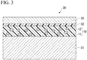
- FIG. 3 is a schematic sectional view of a metal base substrate according to an embodiment of the present invention.
- the metal base substrate 30 of the present embodiment is a laminate in which a metal substrate 31, the above-described insulating film 10, an adhesive layer 32, and a metal foil 33 are laminated in this order.
- the metal substrate 31 is a member which is the base of the metal base substrate 30.
- the insulating film 10 is a member for insulating the metal substrate 31 and the metal foil 33.
- the adhesive layer 32 is a member provided for improving the adhesion between the insulating film 10 and the metal foil 33.
- the adhesive layer 32 preferably includes a resin.
- a resin it is possible to use a silicone resin, an epoxy resin, a polyamide-imide resin, a polyimide resin, or the like.
- the silicone resin includes a modified silicone resin into which various organic groups are introduced.
- the modified silicone resins include polyimide-modified silicone resins, polyester-modified silicone resins, urethane-modified silicone resins, acrylic-modified silicone resins, olefin-modified silicone resins, ether-modified silicone resins, alcohol-modified silicone resins, fluorine-modified silicone resins, amino-modified silicone resins, mercapto-modified silicone resins, and carboxy-modified silicone resins.
- epoxy resins examples include bisphenol A epoxy resins, bisphenol F epoxy resins, novolak epoxy resins, aliphatic epoxy resins, and glycidylamine epoxy resins. Either one of these resins may be used or a combination of two or more of these resins may be used.
- inorganic particles may be dispersed in order to improve thermal conductivity. It is possible to use ceramic particles as the inorganic particles. Examples of the ceramic particles include silica particles, alumina particles, boron nitride particles, titanium oxide particles, alumina-doped silica particles, hydrated alumina particles, and aluminum nitride particles.
- the metal foil 33 is formed in a circuit pattern. Electronic components are bonded via solder on the metal foil 33 formed in the circuit pattern. As a material of the metal foil 33, it is possible to use copper, aluminum, gold, or the like.
- the metal base substrate 30 of the present embodiment by, for example, a method of laminating the insulating film 10 and the adhesive layer 32 on the metal substrate 31 in this order, and then bonding the metal foil 33 on the adhesive layer 32.
- the insulating film 10 by a coating method or an electrodeposition method.
- the adhesive layer 32 by, for example, coating a coating liquid for forming an adhesive layer including a resin for forming an adhesive layer, a solvent, and inorganic particles to be added as necessary, on the surface of the insulating film 10 to form a coated layer, and then, heating and drying the coated layer.
- It is possible to bond the metal foil 33 by overlaying the metal foil 33 on the adhesive layer 32 and then heating the metal foil 33 while applying pressure thereto.
- the metal base substrate 30 of the present embodiment having the above-described configuration, since the above-described insulating film 10 in which both the withstand voltage and the thermal conductivity are improved is disposed as the insulating film between the metal substrate 31 and the metal foil 33, the metal base substrate 30 exhibits excellent voltage endurance (withstand voltage) and heat resistance.
- An insulating film including inorganic particles and a resin was manufactured using the manufacturing method shown in Table 1.
- the specific manufacturing method of the insulating film manufactured in each of the Invention Examples and the Comparative Examples was as follows.
- a 300 mL separable flask was charged with 4,4'-diaminodiphenyl ether and NMP (N-methyl-2-pyrrolidone). The amount of NMP was adjusted such that the concentration of the obtained polyamic acid was 40% by mass. After stirring at room temperature to completely dissolve the 4,4'-diaminodiphenyl ether, a predetermined amount of tetracarboxylic dianhydride was added little by little such that the internal temperature did not exceed 30°C. Thereafter, stirring was continued for 16 hours under a nitrogen atmosphere to prepare a polyamic acid (polyimide precursor) solution.
- NMP N-methyl-2-pyrrolidone
- Ceramic particles shown in Table 1 below were prepared. 1.0 g of the prepared ceramic particles was added to 10 g of NMP and subjected to ultrasonic treatment for 30 minutes to prepare a ceramic particle dispersion.
- the prepared polyamic acid solution, the prepared ceramic particle dispersion, and NMP were mixed such that, finally, the amount of the polyamic acid in the solution was 5% by mass and the amount of the ceramic particles with respect to the total amount of the resin component and the ceramic particles was the volume percentage shown in Table 1 below.
- the obtained mixture was subjected to a dispersion treatment by repeating a high-pressure injection treatment 10 times at a pressure of 50 MPa, using Starburst manufactured by Sugino Machine Limited, to prepare a ceramic particle-dispersed polyamic acid solution.
- the prepared ceramic particle-dispersed polyamic acid solution was coated on a surface of a copper substrate having a thickness of 0.3 mm and a size of 30 mm ⁇ 20 mm such that the film thickness after heating was 20 ⁇ m to form a coated layer.
- the copper substrate on which the coated layer was formed was placed on a hot plate and the temperature was increased from room temperature to 60°C at a temperature increase rate of 3°C/min, heating was carried out at 60°C for 100 minutes, then, the temperature was further increased to 120°C at a temperature increase rate of 1°C/min, and heating was carried out at 120°C for 100 minutes. Thereby, drying was carried out to form a dried film. Thereafter, the dried film was heated at 250°C for 1 minute, and then was heated at 400°C for 1 minute to manufacture a copper substrate with an insulating film.
- a solvent-soluble polyimide and a polyamide-imide were mixed at a weight ratio of 1:1 and the obtained mixture was dissolved in NMP to prepare a mixed solution of a polyimide and a polyamide-imide.
- a copper substrate with an insulating film was manufactured using a coating method in the same manner as in Invention Example 1, except that the mixed solution, the ceramic particle dispersion, and the NMP were mixed such that, finally, the total amount of the polyimide and the polyamide-imide in the solution was 5% by mass and the amount of the ceramic particles was the amount shown in Table 1 below to prepare a ceramic particle-dispersed resin solution.
- a heat-curable, one-component, solvent-soluble epoxy resin was prepared.
- a copper substrate with an insulating film was manufactured using a coating method in the same manner as in Invention Example 1, except that the solvent-soluble epoxy resin, the ceramic dispersion solution, and the NMP were mixed such that, finally, the amount of the epoxy resin in the solution was 8% by mass and the amount of the ceramic particles was the amount shown in Table 1 below to prepare a ceramic particle-dispersed resin solution.
- the temperature of the coated layer of the ceramic particle-dispersed resin solution was increased from room temperature to 60°C at a temperature increase rate of 3°C/min, heating was carried out at 60°C for 100 minutes, then the temperature was further increased to 120°C at a temperature increase rate of 1°C/min, and heating was carried out at 120°C for 100 minutes. Thereby, drying and curing were carried out to form an insulating film.
- Ceramic particles shown in Table 1 below were prepared. 1.0 g of the prepared ceramic particles was added to a mixed solvent including 62.5 g of NMP, 10 g of 1M2P (1-methoxy-2-propanol), and 0.22 g of AE (amino ether), and the mixture was subjected to an ultrasonic treatment for 30 minutes to prepare a ceramic particle dispersion.
- the prepared ceramic particle dispersion was added to 3.3 g of the polyamide-imide solution such that the amount of the ceramic particles with respect to the total amount of the resin component and the ceramic particles was the volume percentage shown in Table 1 below, and thereby, a ceramic particle-dispersed polyamide-imide solution was prepared.
- a copper substrate having a thickness of 0.3 mm and a size of 30 mm ⁇ 20 mm and a stainless steel electrode were immersed in the prepared electrodeposition solution, and a DC voltage of 100 V was applied using the copper substrate as a positive electrode and the stainless steel electrode as a negative electrode to form an electrodeposition film on the surface of the copper substrate.
- the back surface of the copper substrate was protected by putting a protective tape thereon such that an electrodeposition film was not formed thereon.
- the film thickness of the electrodeposition film was adjusted such that the thickness of the insulating film formed by heating was 20 ⁇ m.
- the copper substrate on which the electrodeposition film was formed was heated at 250°C for 3 minutes in an air atmosphere; and thereby, the electrodeposition film was dried to manufacture a copper substrate with an insulating film.
- the withstand voltage was measured using a multifunctional safety tester 7440 manufactured by Keisoku Giken Co., Ltd.
- An electrode ( ⁇ 6 mm) was disposed on the surface of the insulating film of the copper substrate with an insulating film.
- the copper substrate of the copper substrate with an insulating film and the electrode disposed on the surface of the insulating film were connected to a power source and the voltage was increased to 6000 V in 30 seconds.
- the voltage when the current flowing between the copper substrate and the electrode reached 5000 ⁇ A was taken as the withstand voltage of the insulating film.
- An insulating film consisting of a resin was prepared in the same manner as in Invention Examples 1 to 19 and Comparative Examples 1 to 8 except that the ceramic particles were not dispersed, and the withstand voltage was measured by the above-described method.
- the withstand voltage of the insulating film of each of Invention Examples 1 to 19 and Comparative Examples 1 to 8 was calculated as a relative withstand voltage with the withstand voltage of the insulating film consisting of the resin being set to 1.
- the thermal conductivity (thermal conductivity in the thickness direction of the insulating film) was measured by a laser flash method using LFA477 Nanoflash manufactured by NETZSCH-Geratebau GmbH. The thermal conductivity was calculated using a two-layer model which did not consider interfacial thermal resistance.
- the thickness of the copper substrate was set to 0.3 mm as described above and the thermal diffusivity of the copper substrate was set to 117.2 mm 2 /sec.
- An insulating film consisting of a resin was prepared in the same manner as in Invention Examples 1 to 19 and Comparative Examples 1 to 8 except that the ceramic particles were not dispersed, and the thermal conductivity was measured by the above-described method.
- the thermal conductivity of the insulating film of each of Invention Examples 1 to 19 and Comparative Examples 1 to 8 was calculated as a relative thermal conductivity with the thermal conductivity of the insulating film consisting of the resin being set to 1.
- the value obtained by multiplying the relative withstand voltage and the relative heat conductivity together was calculated as the relative performance value. The larger this value is, the smaller the thermal resistance is.
- the insulating film of Comparative Example 1 using polycrystalline particles of ⁇ -alumina had a low thermal conductivity.
- the insulating film of Comparative Example 2 in which the added amount of ⁇ -alumina single crystal particles was smaller than the range of the present invention had a low thermal conductivity.
- the insulating film of Comparative Example 3 in which the added amount of ⁇ -alumina single crystal particles was larger than the range of the present invention had a low withstand voltage.
- the insulating film of Comparative Example 8 using epoxy resin as the resin had a low withstand voltage; and as a result, the relative performance value was 3 or less which was low.
- the resin in the insulating films of Invention Examples 1 to 19, polyimide, polyamide-imide, or a mixture thereof was used as the resin and ⁇ -alumina single crystal particles having an average particle diameter in a range of 0.3 ⁇ m or more and 1.5 ⁇ m or less were used as the ceramic particles and the amount of ⁇ -alumina single crystal particles was in a range of 8% by volume or more and 80% by volume or less, and it was confirmed that in the insulating films of Invention Examples 1 to 19, a withstand voltage and a thermal conductivity were improved in a well-balanced manner and a high relative performance value was exhibited.
- the amount of ⁇ -alumina single crystal particles was in a range of 20% by volume or more and 70% by volume or less, and it was confirmed that in the insulating films of Invention Examples 3 to 6, 8 to 12, and 15 to 18, a withstand voltage and a thermal conductivity were further improved in a well-balanced manner and a high relative performance value of 5.0 or more was exhibited.
- the ceramic particle-dispersed polyamic acid solution prepared in Invention Example 4 was coated on a release film (Unipeel manufactured by UNITIKA Ltd.) such that the film thickness after drying was 20 ⁇ m to form a coated layer.
- the release film on which the coated layer was formed was placed on a hot plate, the temperature was increased from room temperature to 60°C at a temperature increase rate of 3°C/min, heating was carried out at 60°C for 100 minutes, then the temperature was further increased to 120°C at a temperature increase rate of 1°C/min, and heating was carried out at 120°C for 100 minutes. Thereby, drying was carried out to form a dried film.
- the dried film was peeled off the release film to be a self-supporting film
- the dried film was fixed to a stainless steel mold with clips at several portions, and the dried film was heated at 250°C for 1 minute and then heated at 400°C for 1 minute to manufacture a self-supporting insulating film.
- the withstand voltage, the relative withstand voltage, the thermal conductivity, and the relative thermal conductivity were measured, and the performance value was calculated.
- the withstand voltage was 4.5 kV
- the relative withstand voltage was 1.1
- the thermal conductivity was 1.4 w/mK
- the relative thermal conductivity was 7, and the performance value was 7.5.
- the withstand voltage was measured with the same method as described above, except that electrodes ( ⁇ 6 mm) were arranged on both surfaces of the self-supporting insulating film so as to face each other.
- the thermal conductivity was measured with the same method as described above, except that the thermal conductivity was calculated using a one-layer model.
- a ⁇ 3 mm copper wire and a stainless steel electrode were immersed in the electrodeposition solution prepared in Invention Example 16 and a DC voltage of 100 V was applied using the copper wire as a positive electrode and the stainless steel electrode as a negative electrode to form an electrodeposition film on the surface of the copper wire.
- the film thickness of the electrodeposited film was such that the film thickness of the insulating film formed by heating was 20 ⁇ m.
- the copper wire on which the electrodeposited film was formed was heated at 250°C for 3 minutes in an air atmosphere; and thereby, the electrodeposited film was dried to manufacture a copper wire with an insulating film (insulated copper wire).
- the metal base substrate according to Invention Example by laminating a metal substrate, an insulating film, and a metal foil.
- the ceramic particle-dispersed polyamic acid solution prepared in Invention Example 4 was coated on the surface of a copper substrate having a thickness of 1 mm and a size of 20 mm ⁇ 20 mm to form a coated layer such that the film thickness after heating was 20 ⁇ m.
- the copper substrate on which the coated layer was formed was placed on a hot plate, and the temperature was increased from room temperature to 60°C at a temperature increase rate of 3°C/min, heating was carried out at 60°C for 100 minutes, then the temperature was further increased to 120°C at a temperature increase rate of 1°C/min, and heating was carried out at 120°C for 100 minutes; and thereby, drying was carried out to form a dried film.
- the dried film was heated at 250°C for 1 minute and then heated at 400°C for 1 minute to manufacture a copper substrate with an insulating film.
- the thermal conductivity and the withstand voltage of the insulating film of the obtained copper substrate with an insulating film were measured, the thermal conductivity was 1.4 w/mk and the withstand voltage was 4.1 kV.
- a protective tape was put on the back surface of the obtained copper substrate with an insulating film, then the copper substrate was immersed in a polyamide-imide solution having a concentration of 25% by mass to form a coated layer of a polyamide-imide solution on the insulating film.
- the coated layer was heated at 250°C for 30 minutes to form an adhesive layer on the insulating film.
- a copper foil (CF-T4X-SV-18: manufactured by Fukuda Metal Foil & Powder Co., Ltd.) having a thickness of 18 ⁇ m and a width of 1 cm was overlaid on the adhesive layer and then, while a pressure of 5 MPa was applied thereto using a carbon jig, heating was carried out at a temperature of 215°C for 20 minutes in a vacuum to bond the adhesive layer and the copper foil.
- a metal base substrate in which the copper substrate, the insulating film, the adhesive layer, and the copper foil were laminated in this order was manufactured.
- an insulating film having both a high thermal conductivity and a high voltage endurance (withstand voltage), as well as an excellent heat resistance, chemical resistance, and mechanical properties, and it is possible to provide an insulated conductor and a metal base substrate in which this insulating film is used.
Landscapes
- Chemical & Material Sciences (AREA)
- Chemical Kinetics & Catalysis (AREA)
- Health & Medical Sciences (AREA)
- Medicinal Chemistry (AREA)
- Polymers & Plastics (AREA)
- Organic Chemistry (AREA)
- Engineering & Computer Science (AREA)
- Physics & Mathematics (AREA)
- Spectroscopy & Molecular Physics (AREA)
- Manufacturing & Machinery (AREA)
- Microelectronics & Electronic Packaging (AREA)
- Materials Engineering (AREA)
- Laminated Bodies (AREA)
- Insulating Bodies (AREA)
- Organic Insulating Materials (AREA)
- Compositions Of Macromolecular Compounds (AREA)
- Insulated Metal Substrates For Printed Circuits (AREA)
- Inorganic Insulating Materials (AREA)
- Non-Insulated Conductors (AREA)
- Insulated Conductors (AREA)
Abstract
Description
- The present invention relates to an insulating film, an insulated conductor, and a metal base substrate in which the insulating film is used.
- The present application claims priority on Japanese Patent Application No.
2018-018268 filed on February 5, 2018 2018-246997 filed on December 28, 2018 - Insulating films are used as, for example, an insulating film of an insulated conductor used for a coil and a motor, a protective film for protecting a surface of an electronic component such as a semiconductor chip, an LED element, and the like and a surface of a circuit board, and an insulating film of a metal base substrate.
- As an insulating film, a film formed from a resin composition including a resin and an inorganic filler is used. As the resin, resins having high heat resistance, chemical resistance, and mechanical strength, such as polyimide and polyamide-imide, are used.
- Along with increasing operating voltages and increasing integration of electronic components in recent years, the amount of heat generated by such electronic components tends to increase, and there is a demand for insulating films having low thermal resistance and high heat dissipation. As a method for reducing the thermal resistance of the insulating film, there is a method of adding an inorganic filler having high thermal conductivity thereto. However, in the case where an inorganic filler having a large particle diameter is added thereto, there is a problem that in the withstand voltage (dielectric breakdown voltage) is decreased (Non-Patent Document 1).
- The withstand voltage VR of the insulating film is expressed by Equation (1), where h is the film thickness of the insulating film and VF is the withstand voltage per film thickness.

- On the other hand, the thermal resistance R of the insulating film is expressed by Equation (2), where h is the film thickness of the insulating film and λ is the thermal conductivity of the insulating film.

- From Equation (1) and Equation (2), it is possible to express the thermal resistance R of the insulating film by Equation (3).

- From Equation (3), it is understood that the thermal resistance R of the insulating film is proportional to the reciprocal of a value of the withstand voltage VF per film thickness of the insulating film × the thermal conductivity λ. Accordingly, in order to reduce the thermal resistance R of the insulating film, it is important to increase the value (also referred to below as "performance value") of the withstand voltage VF per film thickness of the insulating film × the thermal conductivity λ.
- Patent Documents 1 and 2 discloses that nanoparticles are used as an inorganic filler in order to improve the withstand voltage of an insulating film.
- Patent Document 1 discloses an insulating film in which nanoparticles having an average maximum diameter of 500 nm or less are used as an inorganic filler. Examples of Patent Document 1 describe insulating films in which 2.5% by mass and 5% by mass of nanoparticles were added respectively.
- Patent Document 2 discloses an insulating film which includes a polyamide-imide resin and insulating fine particles having an average primary particle diameter of 200 nm or less. Examples of Patent Document 2 describe an insulating film in which 5% by mass of insulating fine particles were added. However, in general, the thermal conductivity is not greatly improved even in the case where nanoparticles are added to an insulating film.
- Patent Documents 3 and 4 describe insulating films which include both nanoparticles and microparticles as inorganic fillers in order to further improve thermal conductivity.
- Patent Document 3 discloses a resin composition for an electrical insulating material which includes a first inorganic filler having a microparticle size and a second inorganic filler having a nanoparticle size and consisting of a predetermined material.
- Patent Document 4 discloses a resin composition filled with, as inorganic fillers, a thermally conductive inorganic spherical microfiller having a microparticle size, a microfiller having a plate shape, a rod shape, a fiber shape, or a flake shape, and a thermally conductive inorganic nanofiller having a nanoparticle size.
- However, as described in Non-Patent Document 1, there is a problem in that the withstand voltage is decreased in the case where microparticles are added to an insulating film.
- Non Patent Document 1: Journal of International Council on Electrical Engineering, Vol. 2, No. 1, pp. 90-98, 2012
-
- Patent Document 1: United States Patent Publication No.
2007/0116976 - Patent Document 2: Japanese Unexamined Patent Application, First Publication No.
2013-60575 - Patent Document 3: Japanese Unexamined Patent Application, First Publication No.
2009-13227 - Patent Document 4: Japanese Unexamined Patent Application, First Publication No.
2013-159748 - The present invention was made in view of the above-described circumstances, and the present invention aims to provide an insulating film having both a high thermal conductivity and a high voltage endurance (withstand voltage) as well as an excellent heat resistance, chemical resistance, and mechanical properties, an insulated conductor, and a metal base substrate in which this insulating film is used.
- In order to solve the above-described problem, an insulating film of an embodiment of the present invention includes: a resin consisting of a polyimide, a polyamide-imide, or a mixture thereof; and α-alumina single crystal particles having an average particle diameter in a range of 0.3 µm or more and 1.5 µm or less, in which an amount of the α-alumina single crystal particles is in a range of 8% by volume or more and 80% by volume or less.
- According to the insulating film having these features, since the resin consists of polyimide, polyamide-imide, or a mixture thereof, the heat resistance, chemical resistance, and mechanical properties are improved.
- In addition, since fine α-alumina single crystal particles having an average particle diameter in a range of 0.3 µm or more and 1.5 µm or less are contained in an amount of 8% by volume or more and 60% by volume or less, it is possible to improve both the withstand voltage and the thermal conductivity without impairing the excellent heat resistance, chemical resistance, and mechanical properties of resins such as polyimide and polyamide-imide.
- In the insulating film of the present invention, the amount of the α-alumina single crystal particles is preferably in a range of 20% by volume or more and 70% by volume or less. The amount is more preferably in a range of 30% by volume or more and 60% by volume or less.
- In such a case, it is possible to more reliably improve both the withstand voltage and the thermal conductivity.
- In addition, an insulated conductor of the present invention includes: a conductor; and an insulating film provided on a surface of the conductor, in which the insulating film consists of the above-described insulating film.
- According to the insulated conductor having these features, since the insulating film in which both the withstand voltage and the thermal conductivity are improved is provided on the surface of the conductor, the insulated conductor exhibits excellent voltage endurance (withstand voltage) and heat resistance.
- In addition, a metal base substrate of the present invention includes a metal substrate, an insulating film, and a metal foil which are laminated in this order, in which the insulating film consists of the above-described insulating film.
- According to the metal base substrate having these features, since the insulating film in which both the withstand voltage and the thermal conductivity are improved is disposed between the metal substrate and the metal foil, the metal base substrate exhibits excellent voltage endurance (withstand voltage) and heat resistance.
- According to the present invention, it is possible to provide an insulating film having both a high thermal conductivity and a high voltage endurance (withstand voltage), as well as an excellent heat resistance, chemical resistance, and mechanical properties, and it is also possible to provide an insulated conductor and a metal base substrate in which this insulating film is used.
-
-
FIG. 1 is a schematic sectional view of an insulating film according to an embodiment of the present invention. -
FIG. 2 is a schematic sectional view of an insulated conductor according to an embodiment of the present invention. -
FIG. 3 is a schematic sectional view of a metal base substrate according to an embodiment of the present invention. - An insulating film, an insulated conductor, and a metal base substrate according to an embodiment of the present invention will be explained below while referring to the accompanying drawings.
-
FIG. 1 is a schematic sectional view of an insulating film according to an embodiment of the present invention. - As shown in
FIG. 1 , aninsulating film 10 of the present embodiment includes aresin 11 and α-aluminasingle crystal particles 12. - The
resin 11 becomes a base material of theinsulating film 10. Theresin 11 consists of polyimide, polyamide-imide, or a mixture thereof. Since these resins have imide bonds, the resins have excellent heat resistance, chemical stability, and mechanical properties. - The α-alumina
single crystal particles 12 have an action of efficiently improving the withstand voltage and the thermal conductivity of theinsulating film 10. The α-aluminasingle crystal particles 12 are single crystal particles having a crystal structure of α-alumina (α-Al2O3). - It is possible to confirm that the α-alumina particles are single crystal particles, for example, as follows.
- First, the half width of the peak of the α-alumina particles is acquired by the X-ray diffraction method. The acquired half width of the peak is converted into a crystallite diameter (r) according to the Scherrer equation. Separately, the particle diameters of 100 α-alumina particles are measured using a scanning electron microscope (SEM) and the average thereof is calculated as the average particle diameter (D). The ratio (r/D) of the crystallite diameter (r) to the calculated average particle diameter (D) of the α-alumina particles is calculated, and the particles are regarded as single crystal in the case where the ratio (r/D) is 0.8 or more.
- The average particle diameter of the α-alumina
single crystal particles 12 is in a range of 0.3 µm or more and 1.5 µm or less. In the case where the average particle diameter is less than 0.3 µm, aggregated particles are easily formed, and there is a concern that it may be difficult to uniformly disperse the α-aluminasingle crystal particles 12 in theresin 11. In addition, in the case where the α-aluminasingle crystal particles 12 form aggregated particles, the mechanical strength of the insulatingfilm 10 decreases and the insulatingfilm 10 becomes brittle. On the other hand, in the case where the average particle diameter is more than 1.5 µm, there is a concern that the withstand voltage of the insulatingfilm 10 may be decreased. The average particle diameter of the α-aluminasingle crystal particles 12 is preferably in a range of 0.3 µm or more and 0.7 µm or less. - The average particle diameter of the α-alumina
single crystal particles 12 is a value of a volume-based cumulative average diameter (Dv50) measured by a laser diffraction type particle size distribution analyzer using a dispersion of the α-aluminasingle crystal particles 12. The dispersion of the α-aluminasingle crystal particles 12 for measuring the average particle diameter can be prepared by, for example, adding the α-aluminasingle crystal particles 12 together with a dispersant to an N-methyl-2-pyrrolidone (NMP) solvent and dispersing the α-aluminasingle crystal particles 12 by ultrasonic dispersion. - As the α-alumina
single crystal particles 12, for example, it is possible to use AA-03, AA-04, AA-05, AA-07, AA-1.5 of the Advanced Alumina (AA) series sold by Sumitomo Chemical Co., Ltd., and the like. - The amount of the α-alumina
single crystal particles 12 in the insulatingfilm 10 is in a range of 8% by volume or more and 80% by volume or less. In the case where the amount is less than 8% by volume, there is a concern that it may be difficult to improve the thermal conductivity of the insulatingfilm 10. On the other hand, in the case where the amount is more than 80% by volume, the mechanical strength of the insulatingfilm 10 decreases and the insulatingfilm 10 becomes brittle. In addition, there is a concern that it may be difficult to mix theresin 11 and the α-aluminasingle crystal particles 12 and it may be difficult to uniformly disperse the α-aluminasingle crystal particles 12 in theresin 11. From the viewpoint of more reliably improving both the withstand voltage and the thermal conductivity of the insulatingfilm 10, the lower limit of the amount of the α-aluminasingle crystal particles 12 is preferably 20% by volume or more, and particularly preferably 30% by volume or more. In addition, the upper limit of the amount of α-aluminasingle crystal particles 12 is preferably 70% by volume or less, and particularly preferably 60% by volume or less. - It is possible to determine the amount of the α-alumina
single crystal particles 12 in the insulatingfilm 10, for example, as follows. - The insulating
film 10 is heated at 400°C for 12 hours in air to thermally decompose and remove theresin 11, and the remaining α-aluminasingle crystal particles 12 are recovered. The weight of the recovered α-aluminasingle crystal particles 12 is measured and the amount (weight basis) (% by weight) of the α-aluminasingle crystal particles 12 is calculated from the weight of the insulatingfilm 10 before heating. The amount on a weight basis is converted to an amount on a volume basis (% by volume) using the density of the resin and the density of α-alumina. - Specifically, when the weight of the α-alumina particles recovered after heating is Wa (g), the weight of the insulating film before heating is Wf (g), the density of α-alumina is Da (g/cm3), and the density of the resin is Dr (g/cm3), the amount (% by weight) of α-alumina single crystal particles is calculated from the following equation.

- Next, the amount (% by volume) of α-alumina single crystal particles is calculated by the following equation.

- The film thickness of the insulating
film 10 varies depending on the application, but is usually in a range of 1 µm or more and 200 µm or less, and preferably in a range of 10 µm or more and 50 µm or less. - It is possible to use the insulating
film 10 of the present embodiment as an insulating film of an insulated conductor used for a coil or a motor as is the case with, for example, an enamel film of an enameled wire. In addition, it is possible to use the insulatingfilm 10 as a protective film for protecting the surface of an electronic component or a circuit board. Furthermore, in a metal base substrate or the like, it is possible to use the insulatingfilm 10 as an insulating film disposed between a metal foil (circuit pattern) and the substrate. In addition, the insulatingfilm 10 is processed into a single sheet or a film, and this sheet or film can be used as, for example, an insulating material for a circuit board such as a flexible printed board and the like. - In the electrodeposition method, an electrodeposition solution including either one of a polyimide or polyamide-imide, a solvent, water, a poor solvent, and a base is electrodeposited on the surface of the conductive substrate to form an electrodeposition film, and then the electrodeposition film is dried, and the obtained dried film is heated and cured.
- The insulating film of the present embodiment can be formed by, for example, a coating method or an electrodeposition method.
- In the coating method, a resin material consisting of polyimide, polyamide-imide, a precursor thereof, or a mixture thereof is dissolved in a solution, and α-alumina single crystal particles are dispersed in the solution to prepare an α-alumina single crystal particle-dispersed resin solution. Next, the α-alumina single crystal particle-dispersed resin solution is coated on a substrate to form a coated layer. Next, the coated layer is dried and the obtained dried film is heated and cured. As the method of coating the α-alumina single crystal particle-dispersed resin solution on the surface of a metal substrate, it is possible to use a spin coating method, a bar coating method, a knife coating method, a roll coating method, a blade coating method, a die coating method, a gravure coating method, a dip coating method, and the like.
- According to the insulating
film 10 of the present embodiment having the above-described configuration, since theresin 11 consists of polyimide, polyamide-imide, or a mixture thereof, the heat resistance, chemical resistance, and mechanical properties are improved. In addition, since the fine α-aluminasingle crystal particles 12 having an average particle diameter in a range of 0.3 µm or more and 1.5 µm or less are contained in an amount of 8% by volume or more and 80% by volume or less, it is possible to improve both the withstand voltage and the thermal conductivity without impairing the excellent heat resistance, chemical resistance, and mechanical properties of resins such as polyimide and polyamide-imide. - In addition, according to the insulating
film 10 of the present embodiment, it is possible to more reliably improve both the withstand voltage and the thermal conductivity by setting the amount of the α-aluminasingle crystal particles 12 to be in a range of 20% by volume or more and 70% by volume or less, and more preferably in a range of 30% by volume or more and 60% by volume or less. - Next, an insulated conductor according to an embodiment of the present invention will be explained. Parts where the configuration is the same as that of the above-described insulating film are denoted by the same reference numerals and detailed explanation thereof is omitted.
-
FIG. 2 is a schematic sectional view of an insulated conductor according to an embodiment of the present invention. - As shown in
FIG. 2 , theinsulated conductor 20 according to the present embodiment includes aconductor 21, and the above-described insulatingfilm 10 provided on the surface of theconductor 21. - The
conductor 21 consists of a metal having high conductivity. As theconductor 21, it is possible to use, for example, copper, a copper alloy, aluminum, or an aluminum alloy. InFIG. 2 , the cross-section of theconductor 21 is circular, but the cross-section shape of theconductor 21 is not particularly limited, and may be, for example, an ellipse or a square. - The insulating
film 10 is a member for insulating theconductor 21 from the outside. - It is possible to manufacture the
insulated conductor 20 of the present embodiment by, for example, forming an insulating film on the surface of the conductor by a coating method or an electrodeposition method. - In the
insulated conductor 20 of the present embodiment having the above-described configuration, since the insulatingfilm 10 in which both the withstand voltage and the thermal conductivity are improved is provided as an insulating film on the surface of theconductor 21, theinsulated conductor 20 exhibits excellent voltage endurance (withstand voltage) and heat resistance. - Next, a metal base substrate according to an embodiment of the present invention will be explained. Parts where the configuration is the same as that of the above-described insulating film are denoted by the same reference numerals and detailed explanation thereof is omitted.
-
FIG. 3 is a schematic sectional view of a metal base substrate according to an embodiment of the present invention. - As shown in
FIG. 3 , themetal base substrate 30 of the present embodiment is a laminate in which ametal substrate 31, the above-described insulatingfilm 10, anadhesive layer 32, and ametal foil 33 are laminated in this order. - The
metal substrate 31 is a member which is the base of themetal base substrate 30. As themetal substrate 31, it is possible to use a copper plate, an aluminum plate, and laminated plates thereof. - The insulating
film 10 is a member for insulating themetal substrate 31 and themetal foil 33. - The
adhesive layer 32 is a member provided for improving the adhesion between the insulatingfilm 10 and themetal foil 33. - The
adhesive layer 32 preferably includes a resin. As the resin, it is possible to use a silicone resin, an epoxy resin, a polyamide-imide resin, a polyimide resin, or the like. The silicone resin includes a modified silicone resin into which various organic groups are introduced. Examples of the modified silicone resins include polyimide-modified silicone resins, polyester-modified silicone resins, urethane-modified silicone resins, acrylic-modified silicone resins, olefin-modified silicone resins, ether-modified silicone resins, alcohol-modified silicone resins, fluorine-modified silicone resins, amino-modified silicone resins, mercapto-modified silicone resins, and carboxy-modified silicone resins. Examples of the epoxy resins include bisphenol A epoxy resins, bisphenol F epoxy resins, novolak epoxy resins, aliphatic epoxy resins, and glycidylamine epoxy resins. Either one of these resins may be used or a combination of two or more of these resins may be used. - In the
adhesive layer 32, inorganic particles may be dispersed in order to improve thermal conductivity. It is possible to use ceramic particles as the inorganic particles. Examples of the ceramic particles include silica particles, alumina particles, boron nitride particles, titanium oxide particles, alumina-doped silica particles, hydrated alumina particles, and aluminum nitride particles. - The
metal foil 33 is formed in a circuit pattern. Electronic components are bonded via solder on themetal foil 33 formed in the circuit pattern. As a material of themetal foil 33, it is possible to use copper, aluminum, gold, or the like. - It is possible to manufacture the
metal base substrate 30 of the present embodiment by, for example, a method of laminating the insulatingfilm 10 and theadhesive layer 32 on themetal substrate 31 in this order, and then bonding themetal foil 33 on theadhesive layer 32. It is possible to form the insulatingfilm 10 by a coating method or an electrodeposition method. It is possible to form theadhesive layer 32 by, for example, coating a coating liquid for forming an adhesive layer including a resin for forming an adhesive layer, a solvent, and inorganic particles to be added as necessary, on the surface of the insulatingfilm 10 to form a coated layer, and then, heating and drying the coated layer. It is possible to bond themetal foil 33 by overlaying themetal foil 33 on theadhesive layer 32 and then heating themetal foil 33 while applying pressure thereto. - According to the
metal base substrate 30 of the present embodiment having the above-described configuration, since the above-described insulatingfilm 10 in which both the withstand voltage and the thermal conductivity are improved is disposed as the insulating film between themetal substrate 31 and themetal foil 33, themetal base substrate 30 exhibits excellent voltage endurance (withstand voltage) and heat resistance. - Next, the effects of the present invention will be explained with reference to Examples.
- An insulating film including inorganic particles and a resin was manufactured using the manufacturing method shown in Table 1. The specific manufacturing method of the insulating film manufactured in each of the Invention Examples and the Comparative Examples was as follows.
- A 300 mL separable flask was charged with 4,4'-diaminodiphenyl ether and NMP (N-methyl-2-pyrrolidone). The amount of NMP was adjusted such that the concentration of the obtained polyamic acid was 40% by mass. After stirring at room temperature to completely dissolve the 4,4'-diaminodiphenyl ether, a predetermined amount of tetracarboxylic dianhydride was added little by little such that the internal temperature did not exceed 30°C. Thereafter, stirring was continued for 16 hours under a nitrogen atmosphere to prepare a polyamic acid (polyimide precursor) solution.
- Ceramic particles shown in Table 1 below were prepared. 1.0 g of the prepared ceramic particles was added to 10 g of NMP and subjected to ultrasonic treatment for 30 minutes to prepare a ceramic particle dispersion.
- Next, the prepared polyamic acid solution, the prepared ceramic particle dispersion, and NMP were mixed such that, finally, the amount of the polyamic acid in the solution was 5% by mass and the amount of the ceramic particles with respect to the total amount of the resin component and the ceramic particles was the volume percentage shown in Table 1 below. Subsequently, the obtained mixture was subjected to a dispersion treatment by repeating a high-
pressure injection treatment 10 times at a pressure of 50 MPa, using Starburst manufactured by Sugino Machine Limited, to prepare a ceramic particle-dispersed polyamic acid solution. - The prepared ceramic particle-dispersed polyamic acid solution was coated on a surface of a copper substrate having a thickness of 0.3 mm and a size of 30 mm × 20 mm such that the film thickness after heating was 20 µm to form a coated layer. Next, the copper substrate on which the coated layer was formed was placed on a hot plate and the temperature was increased from room temperature to 60°C at a temperature increase rate of 3°C/min, heating was carried out at 60°C for 100 minutes, then, the temperature was further increased to 120°C at a temperature increase rate of 1°C/min, and heating was carried out at 120°C for 100 minutes. Thereby, drying was carried out to form a dried film. Thereafter, the dried film was heated at 250°C for 1 minute, and then was heated at 400°C for 1 minute to manufacture a copper substrate with an insulating film.
- A solvent-soluble polyimide and a polyamide-imide were mixed at a weight ratio of 1:1 and the obtained mixture was dissolved in NMP to prepare a mixed solution of a polyimide and a polyamide-imide. A copper substrate with an insulating film was manufactured using a coating method in the same manner as in Invention Example 1, except that the mixed solution, the ceramic particle dispersion, and the NMP were mixed such that, finally, the total amount of the polyimide and the polyamide-imide in the solution was 5% by mass and the amount of the ceramic particles was the amount shown in Table 1 below to prepare a ceramic particle-dispersed resin solution.
- A heat-curable, one-component, solvent-soluble epoxy resin was prepared. A copper substrate with an insulating film was manufactured using a coating method in the same manner as in Invention Example 1, except that the solvent-soluble epoxy resin, the ceramic dispersion solution, and the NMP were mixed such that, finally, the amount of the epoxy resin in the solution was 8% by mass and the amount of the ceramic particles was the amount shown in Table 1 below to prepare a ceramic particle-dispersed resin solution. The temperature of the coated layer of the ceramic particle-dispersed resin solution was increased from room temperature to 60°C at a temperature increase rate of 3°C/min, heating was carried out at 60°C for 100 minutes, then the temperature was further increased to 120°C at a temperature increase rate of 1°C/min, and heating was carried out at 120°C for 100 minutes. Thereby, drying and curing were carried out to form an insulating film.
- Ceramic particles shown in Table 1 below were prepared. 1.0 g of the prepared ceramic particles was added to a mixed solvent including 62.5 g of NMP, 10 g of 1M2P (1-methoxy-2-propanol), and 0.22 g of AE (amino ether), and the mixture was subjected to an ultrasonic treatment for 30 minutes to prepare a ceramic particle dispersion.
- Next, the prepared ceramic particle dispersion was added to 3.3 g of the polyamide-imide solution such that the amount of the ceramic particles with respect to the total amount of the resin component and the ceramic particles was the volume percentage shown in Table 1 below, and thereby, a ceramic particle-dispersed polyamide-imide solution was prepared.
- While stirring the prepared ceramic particle-dispersed polyamide-imide solution at a rotation speed of 5000 rpm, 21 g of water was added dropwise to the ceramic particle-dispersed polyamide-imide solution to prepare a ceramic particle-dispersed polyamide-imide electrodeposition solution.
- A copper substrate having a thickness of 0.3 mm and a size of 30 mm × 20 mm and a stainless steel electrode were immersed in the prepared electrodeposition solution, and a DC voltage of 100 V was applied using the copper substrate as a positive electrode and the stainless steel electrode as a negative electrode to form an electrodeposition film on the surface of the copper substrate. The back surface of the copper substrate was protected by putting a protective tape thereon such that an electrodeposition film was not formed thereon. The film thickness of the electrodeposition film was adjusted such that the thickness of the insulating film formed by heating was 20 µm. Next, the copper substrate on which the electrodeposition film was formed was heated at 250°C for 3 minutes in an air atmosphere; and thereby, the electrodeposition film was dried to manufacture a copper substrate with an insulating film.
- The following items were evaluated for the insulating films manufactured in Invention Examples 1 to 19 and Comparative Examples 1 to 8. The results are shown in Table 1.
- The withstand voltage was measured using a multifunctional safety tester 7440 manufactured by Keisoku Giken Co., Ltd. An electrode (Φ6 mm) was disposed on the surface of the insulating film of the copper substrate with an insulating film. The copper substrate of the copper substrate with an insulating film and the electrode disposed on the surface of the insulating film were connected to a power source and the voltage was increased to 6000 V in 30 seconds. The voltage when the current flowing between the copper substrate and the electrode reached 5000 µA was taken as the withstand voltage of the insulating film.
- An insulating film consisting of a resin was prepared in the same manner as in Invention Examples 1 to 19 and Comparative Examples 1 to 8 except that the ceramic particles were not dispersed, and the withstand voltage was measured by the above-described method. The withstand voltage of the insulating film of each of Invention Examples 1 to 19 and Comparative Examples 1 to 8 was calculated as a relative withstand voltage with the withstand voltage of the insulating film consisting of the resin being set to 1.
- The thermal conductivity (thermal conductivity in the thickness direction of the insulating film) was measured by a laser flash method using LFA477 Nanoflash manufactured by NETZSCH-Geratebau GmbH. The thermal conductivity was calculated using a two-layer model which did not consider interfacial thermal resistance. The thickness of the copper substrate was set to 0.3 mm as described above and the thermal diffusivity of the copper substrate was set to 117.2 mm2/sec. In order to calculate the thermal conductivity of the insulating film, the density of α-alumina particles of 3.89 g/cm3, the specific heat of α-alumina particles of 0.78 J/gK, the density of silica particles of 2.2 g/cm3, the specific heat of silica particles of 0.76 J/gK, the density of boron nitride of 2.1 g/cm3, the specific heat of boron nitride of 0.8 J/gK, the density of polyamide-imide resin of 1.41 g/cm3, the specific heat of polyamide-imide resin of 1.09 J/gK, the density of polyimide of 1.4 g/cm3, the specific heat of polyimide of 1.13 J/gK, the density of epoxy resin of 1.2 g/cm3, and the specific heat of epoxy resin of 1.05 J/gK were used.
- An insulating film consisting of a resin was prepared in the same manner as in Invention Examples 1 to 19 and Comparative Examples 1 to 8 except that the ceramic particles were not dispersed, and the thermal conductivity was measured by the above-described method. The thermal conductivity of the insulating film of each of Invention Examples 1 to 19 and Comparative Examples 1 to 8 was calculated as a relative thermal conductivity with the thermal conductivity of the insulating film consisting of the resin being set to 1.
- The value obtained by multiplying the relative withstand voltage and the relative heat conductivity together was calculated as the relative performance value. The larger this value is, the smaller the thermal resistance is.
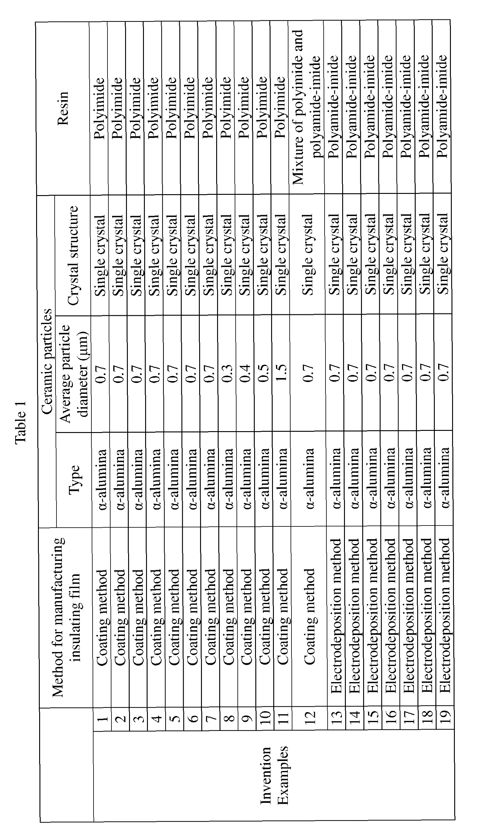


- The insulating film of Comparative Example 1 using polycrystalline particles of α-alumina had a low thermal conductivity. The insulating film of Comparative Example 2 in which the added amount of α-alumina single crystal particles was smaller than the range of the present invention had a low thermal conductivity. The insulating film of Comparative Example 3 in which the added amount of α-alumina single crystal particles was larger than the range of the present invention had a low withstand voltage. The insulating films of Comparative Examples 4 and 5, in which the average particle diameter of α-alumina single crystal particles was larger than the range of the present invention, had a low withstand voltage. The insulating film of Comparative Example 6, in which silica nanoparticles were used instead of α-alumina single crystal particles, had both a low withstand voltage and a low thermal conductivity. The insulating film of Comparative Example 7, in which boron nitride nanoparticles were used instead of α-alumina single crystal particles, had a low withstand voltage. Furthermore, the insulating film of Comparative Example 8 using epoxy resin as the resin had a low withstand voltage; and as a result, the relative performance value was 3 or less which was low.
- On the other hand, in the insulating films of Invention Examples 1 to 19, polyimide, polyamide-imide, or a mixture thereof was used as the resin and α-alumina single crystal particles having an average particle diameter in a range of 0.3 µm or more and 1.5 µm or less were used as the ceramic particles and the amount of α-alumina single crystal particles was in a range of 8% by volume or more and 80% by volume or less, and it was confirmed that in the insulating films of Invention Examples 1 to 19, a withstand voltage and a thermal conductivity were improved in a well-balanced manner and a high relative performance value was exhibited. In particular, in the insulating films of Invention Examples 3 to 6, 8 to 12, and 15 to 18, the amount of α-alumina single crystal particles was in a range of 20% by volume or more and 70% by volume or less, and it was confirmed that in the insulating films of Invention Examples 3 to 6, 8 to 12, and 15 to 18, a withstand voltage and a thermal conductivity were further improved in a well-balanced manner and a high relative performance value of 5.0 or more was exhibited.
- The ceramic particle-dispersed polyamic acid solution prepared in Invention Example 4 was coated on a release film (Unipeel manufactured by UNITIKA Ltd.) such that the film thickness after drying was 20 µm to form a coated layer. Next, the release film on which the coated layer was formed was placed on a hot plate, the temperature was increased from room temperature to 60°C at a temperature increase rate of 3°C/min, heating was carried out at 60°C for 100 minutes, then the temperature was further increased to 120°C at a temperature increase rate of 1°C/min, and heating was carried out at 120°C for 100 minutes. Thereby, drying was carried out to form a dried film. Then, after the dried film was peeled off the release film to be a self-supporting film, the dried film was fixed to a stainless steel mold with clips at several portions, and the dried film was heated at 250°C for 1 minute and then heated at 400°C for 1 minute to manufacture a self-supporting insulating film.
- With respect to the manufactured self-supporting insulating film, the withstand voltage, the relative withstand voltage, the thermal conductivity, and the relative thermal conductivity were measured, and the performance value was calculated. As a result, the withstand voltage was 4.5 kV, the relative withstand voltage was 1.1, the thermal conductivity was 1.4 w/mK, the relative thermal conductivity was 7, and the performance value was 7.5.
- The withstand voltage was measured with the same method as described above, except that electrodes (Φ6 mm) were arranged on both surfaces of the self-supporting insulating film so as to face each other. The thermal conductivity was measured with the same method as described above, except that the thermal conductivity was calculated using a one-layer model.
- It is possible to manufacture the insulated conductor according to Invention Example by coating a conductive wire with an insulating film.
- A Φ3 mm copper wire and a stainless steel electrode were immersed in the electrodeposition solution prepared in Invention Example 16 and a DC voltage of 100 V was applied using the copper wire as a positive electrode and the stainless steel electrode as a negative electrode to form an electrodeposition film on the surface of the copper wire. The film thickness of the electrodeposited film was such that the film thickness of the insulating film formed by heating was 20 µm. Next, the copper wire on which the electrodeposited film was formed was heated at 250°C for 3 minutes in an air atmosphere; and thereby, the electrodeposited film was dried to manufacture a copper wire with an insulating film (insulated copper wire).
- It is possible to manufacture the metal base substrate according to Invention Example by laminating a metal substrate, an insulating film, and a metal foil.
- The ceramic particle-dispersed polyamic acid solution prepared in Invention Example 4 was coated on the surface of a copper substrate having a thickness of 1 mm and a size of 20 mm × 20 mm to form a coated layer such that the film thickness after heating was 20 µm. Next, the copper substrate on which the coated layer was formed was placed on a hot plate, and the temperature was increased from room temperature to 60°C at a temperature increase rate of 3°C/min, heating was carried out at 60°C for 100 minutes, then the temperature was further increased to 120°C at a temperature increase rate of 1°C/min, and heating was carried out at 120°C for 100 minutes; and thereby, drying was carried out to form a dried film. Thereafter, the dried film was heated at 250°C for 1 minute and then heated at 400°C for 1 minute to manufacture a copper substrate with an insulating film. When the thermal conductivity and the withstand voltage of the insulating film of the obtained copper substrate with an insulating film were measured, the thermal conductivity was 1.4 w/mk and the withstand voltage was 4.1 kV.
- A protective tape was put on the back surface of the obtained copper substrate with an insulating film, then the copper substrate was immersed in a polyamide-imide solution having a concentration of 25% by mass to form a coated layer of a polyamide-imide solution on the insulating film.
- Next, the coated layer was heated at 250°C for 30 minutes to form an adhesive layer on the insulating film.
- Next, a copper foil (CF-T4X-SV-18: manufactured by Fukuda Metal Foil & Powder Co., Ltd.) having a thickness of 18 µm and a width of 1 cm was overlaid on the adhesive layer and then, while a pressure of 5 MPa was applied thereto using a carbon jig, heating was carried out at a temperature of 215°C for 20 minutes in a vacuum to bond the adhesive layer and the copper foil. As described above, a metal base substrate in which the copper substrate, the insulating film, the adhesive layer, and the copper foil were laminated in this order was manufactured.
- According to Invention Examples, it is possible to provide an insulating film having both a high thermal conductivity and a high voltage endurance (withstand voltage), as well as an excellent heat resistance, chemical resistance, and mechanical properties, and it is possible to provide an insulated conductor and a metal base substrate in which this insulating film is used.
-
- 10 Insulating film
- 11 Resin
- 12 α-alumina single crystal particles
- 20 Insulated conductor
- 21 Conductor
- 30 Metal base substrate
- 31 Metal substrate
- 32 Adhesive layer
- 33 Metal foil
Claims (4)
- An insulating film comprising:a resin consisting of a polyimide, a polyamide-imide, or a mixture thereof; andα-alumina single crystal particles having an average particle diameter in a range of 0.3 µm or more and 1.5 µm or less,wherein an amount of the α-alumina single crystal particles is in a range of 8% by volume or more and 80% by volume or less.
- The insulating film according to claim 1,
wherein the amount of the α-alumina single crystal particles is in a range of 20% by volume or more and 70% by volume or less. - An insulated conductor comprising:a conductor; andan insulating film provided on a surface of the conductor,wherein the insulating film consists of the insulating film according to claim 1 or 2.
- A metal base substrate comprising:a metal substrate;an insulating film; anda metal foil, which are laminated in this order,wherein the insulating film consists of the insulating film according to claim 1 or 2.
Applications Claiming Priority (3)
| Application Number | Priority Date | Filing Date | Title |
|---|---|---|---|
| JP2018018268 | 2018-02-05 | ||
| JP2018246997A JP6562147B2 (en) | 2018-02-05 | 2018-12-28 | Insulating film, insulated conductor, metal base substrate |
| PCT/JP2019/003650 WO2019151488A1 (en) | 2018-02-05 | 2019-02-01 | Insulating film, insulated conductor, metal base substrate |
Publications (2)
| Publication Number | Publication Date |
|---|---|
| EP3699932A1 true EP3699932A1 (en) | 2020-08-26 |
| EP3699932A4 EP3699932A4 (en) | 2021-08-18 |
Family
ID=67690467
Family Applications (1)
| Application Number | Title | Priority Date | Filing Date |
|---|---|---|---|
| EP19747896.9A Withdrawn EP3699932A4 (en) | 2018-02-05 | 2019-02-01 | Insulating film, insulated conductor, metal base substrate |
Country Status (7)
| Country | Link |
|---|---|
| US (1) | US20210166844A1 (en) |
| EP (1) | EP3699932A4 (en) |
| JP (1) | JP6562147B2 (en) |
| KR (1) | KR20200117985A (en) |
| CN (1) | CN111448620B (en) |
| PH (1) | PH12020500566A1 (en) |
| TW (1) | TWI770355B (en) |
Families Citing this family (5)
| Publication number | Priority date | Publication date | Assignee | Title |
|---|---|---|---|---|
| JP2021116838A (en) * | 2020-01-23 | 2021-08-10 | マツダ株式会社 | Friction material and friction fastening device |
| JP7532947B2 (en) * | 2020-06-26 | 2024-08-14 | 三菱マテリアル株式会社 | Insulating heat dissipation material, insulating film, and method for producing insulating film |
| JP7482763B2 (en) * | 2020-11-30 | 2024-05-14 | 日本特殊陶業株式会社 | coil |
| JP7711392B2 (en) | 2021-02-25 | 2025-07-23 | 三菱マテリアル株式会社 | Polyimide resin composition and metal base substrate |
| CN114724787B (en) * | 2022-05-16 | 2022-11-15 | 醴陵市东方电瓷电器有限公司 | Electric porcelain insulator for extra-high voltage line and preparation method thereof |
Family Cites Families (26)
| Publication number | Priority date | Publication date | Assignee | Title |
|---|---|---|---|---|
| JPS6352496A (en) * | 1986-08-21 | 1988-03-05 | 三菱電線工業株式会社 | Circuit board |
| JPH09204823A (en) * | 1995-11-24 | 1997-08-05 | Showa Electric Wire & Cable Co Ltd | Insulated wire and electric equipment using the same |
| JP4281880B2 (en) * | 1996-02-13 | 2009-06-17 | ゼネラル・エレクトリック・カナダ | High corona resistant sandwich insulation |
| JP3496636B2 (en) * | 2000-02-16 | 2004-02-16 | 日立電線株式会社 | Paint for partial discharge resistant enameled wire and partial discharge resistant enameled wire |
| CN1910122A (en) * | 2004-01-08 | 2007-02-07 | 昭和电工株式会社 | Inorganic powder, resin composition filled with the powder and use thereof |
| JP2005272714A (en) * | 2004-03-25 | 2005-10-06 | Tokyo Magnetic Printing Co Ltd | Insulating magnetic paint |
| JP2006134813A (en) * | 2004-11-09 | 2006-05-25 | Sumitomo Electric Ind Ltd | Insulation coating material and insulation coating conductor |
| US20070116976A1 (en) | 2005-11-23 | 2007-05-24 | Qi Tan | Nanoparticle enhanced thermoplastic dielectrics, methods of manufacture thereof, and articles comprising the same |
| US8354091B2 (en) * | 2006-10-31 | 2013-01-15 | Denki Kagaku Kogyo Kabushiki Kaisha | Alumina powder and method for preparing the same as well as use thereof |
| JP2009013227A (en) | 2007-07-02 | 2009-01-22 | Tokyo Electric Power Co Inc:The | Resin composition for electrical insulating material and method for producing the same |
| CN102190323B (en) * | 2010-02-25 | 2014-08-06 | 住友化学株式会社 | Inorganic oxide powder, slurry containing inorganic oxide, lithium ion secondary battery having the slurry and preparation method thereof |
| WO2011111684A1 (en) * | 2010-03-10 | 2011-09-15 | 新日鐵化学株式会社 | Thermally conductive polyimide film and thermally conductive laminate produced using same |
| KR101957532B1 (en) * | 2010-12-01 | 2019-03-12 | 도레이 카부시키가이샤 | Adhesive composition, adhesive sheet, and semiconductor device using the adhesive composition or the adhesive sheet |
| JP2012213900A (en) * | 2011-03-31 | 2012-11-08 | Nippon Steel Chem Co Ltd | Heat conductive polyimide-metal substrate |
| JP2012213899A (en) * | 2011-03-31 | 2012-11-08 | Nippon Steel Chem Co Ltd | Heat conductive polyimide-metal substrate |
| WO2012172972A1 (en) * | 2011-06-14 | 2012-12-20 | 新日鉄住金化学株式会社 | Cross-linked polyimide resin and method for producing same, adhesive resin composition and cured product thereof, cover lay film, circuit board, heat-conductive substrate, and heat-conductive polyimide film |
| JP5650084B2 (en) * | 2011-06-22 | 2015-01-07 | 新日鉄住金化学株式会社 | Thermally conductive substrate and thermally conductive polyimide film |
| JP5859915B2 (en) * | 2011-08-25 | 2016-02-16 | 日東電工株式会社 | Insulation film |
| JP2013159748A (en) | 2012-02-08 | 2013-08-19 | Kyushu Institute Of Technology | Resin composition, and method for producing the same |
| JP2014183300A (en) * | 2013-03-21 | 2014-09-29 | Shindo Denshi Kogyo Kk | Heating component wiring board and heating component mounting module |
| EP3015487B1 (en) * | 2013-06-27 | 2018-04-04 | Hitachi Chemical Co., Ltd. | Resin composition, resin sheet, cured resin sheet, resin sheet structure, cured resin sheet structure, method for producing cured resin sheet structure, semiconductor device, and led device |
| WO2017007000A1 (en) * | 2015-07-09 | 2017-01-12 | 住友精化株式会社 | Electrical insulating resin composition for partial-discharge resistance |
| WO2018025538A1 (en) * | 2016-08-01 | 2018-02-08 | 三菱マテリアル株式会社 | Insulating film |
| JP2018026320A (en) * | 2016-08-01 | 2018-02-15 | 三菱マテリアル株式会社 | Insulation film |
| WO2018030079A1 (en) * | 2016-08-08 | 2018-02-15 | 東レ株式会社 | Resin composition, sheet obtained therefrom, laminate, power semiconductor device, plasma processing apparatus, and process for producing semiconductor |
| JP7143659B2 (en) * | 2018-07-18 | 2022-09-29 | 三菱マテリアル株式会社 | metal base substrate |
-
2018
- 2018-12-28 JP JP2018246997A patent/JP6562147B2/en not_active Expired - Fee Related
-
2019
- 2019-02-01 TW TW108104032A patent/TWI770355B/en not_active IP Right Cessation
- 2019-02-01 EP EP19747896.9A patent/EP3699932A4/en not_active Withdrawn
- 2019-02-01 KR KR1020207016740A patent/KR20200117985A/en not_active Ceased
- 2019-02-01 CN CN201980006171.6A patent/CN111448620B/en active Active
- 2019-02-01 US US16/770,694 patent/US20210166844A1/en not_active Abandoned
-
2020
- 2020-06-25 PH PH12020500566A patent/PH12020500566A1/en unknown
Also Published As
| Publication number | Publication date |
|---|---|
| CN111448620B (en) | 2022-08-05 |
| JP2019140094A (en) | 2019-08-22 |
| CN111448620A (en) | 2020-07-24 |
| TW201936790A (en) | 2019-09-16 |
| US20210166844A1 (en) | 2021-06-03 |
| TWI770355B (en) | 2022-07-11 |
| PH12020500566A1 (en) | 2021-04-19 |
| KR20200117985A (en) | 2020-10-14 |
| JP6562147B2 (en) | 2019-08-21 |
| EP3699932A4 (en) | 2021-08-18 |
Similar Documents
| Publication | Publication Date | Title |
|---|---|---|
| US20210166844A1 (en) | Insulating film, insulated conductor, metal base substrate | |
| CN109155165B (en) | insulating film | |
| KR102357814B1 (en) | insulating film | |
| TWI751292B (en) | Heat radiating circuit substrate | |
| JP2017022265A (en) | Metal circuit board and method for manufacturing the same | |
| EP3749069A1 (en) | Metal base substrate | |
| JP6021150B2 (en) | Low temperature resistant resin composition and superconducting wire using the same | |
| WO2019151488A1 (en) | Insulating film, insulated conductor, metal base substrate | |
| JP7508824B2 (en) | Insulating film, metal base substrate, and method for manufacturing metal base substrate | |
| JP2017197648A (en) | Resin composition for circuit board and metal base circuit board using the same | |
| JP2021152102A (en) | Insulation film, metal base substrate and metal base substrate production method | |
| EP4299649A1 (en) | Polyimide resin composition and metal-based substrate | |
| JP7468190B2 (en) | Insulating heat dissipation material, insulating film, and method for producing insulating film | |
| JP7532947B2 (en) | Insulating heat dissipation material, insulating film, and method for producing insulating film | |
| JP2019169619A (en) | Metal base substrate and module | |
| JP7259206B2 (en) | metal base substrate |
Legal Events
| Date | Code | Title | Description |
|---|---|---|---|
| STAA | Information on the status of an ep patent application or granted ep patent |
Free format text: STATUS: THE INTERNATIONAL PUBLICATION HAS BEEN MADE |
|
| PUAI | Public reference made under article 153(3) epc to a published international application that has entered the european phase |
Free format text: ORIGINAL CODE: 0009012 |
|
| STAA | Information on the status of an ep patent application or granted ep patent |
Free format text: STATUS: REQUEST FOR EXAMINATION WAS MADE |
|
| 17P | Request for examination filed |
Effective date: 20200520 |
|
| AK | Designated contracting states |
Kind code of ref document: A1 Designated state(s): AL AT BE BG CH CY CZ DE DK EE ES FI FR GB GR HR HU IE IS IT LI LT LU LV MC MK MT NL NO PL PT RO RS SE SI SK SM TR |
|
| AX | Request for extension of the european patent |
Extension state: BA ME |
|
| TPAC | Observations filed by third parties |
Free format text: ORIGINAL CODE: EPIDOSNTIPA |
|
| DAV | Request for validation of the european patent (deleted) | ||
| DAX | Request for extension of the european patent (deleted) | ||
| A4 | Supplementary search report drawn up and despatched |
Effective date: 20210721 |
|
| RIC1 | Information provided on ipc code assigned before grant |
Ipc: H01B 3/30 20060101AFI20210715BHEP Ipc: C08L 79/08 20060101ALI20210715BHEP Ipc: H01B 3/00 20060101ALI20210715BHEP Ipc: H01B 7/02 20060101ALI20210715BHEP Ipc: H01B 17/62 20060101ALI20210715BHEP Ipc: H05K 1/05 20060101ALI20210715BHEP Ipc: C08G 73/14 20060101ALI20210715BHEP |
|
| STAA | Information on the status of an ep patent application or granted ep patent |
Free format text: STATUS: EXAMINATION IS IN PROGRESS |
|
| STAA | Information on the status of an ep patent application or granted ep patent |
Free format text: STATUS: THE APPLICATION HAS BEEN WITHDRAWN |
|
| 17Q | First examination report despatched |
Effective date: 20240109 |
|
| 18W | Application withdrawn |
Effective date: 20240122 |