EP3698429B1 - Hf-mems-übertragungsvorrichtungen mit hoher impedanz und verfahren zu ihrer herstellung - Google Patents
Hf-mems-übertragungsvorrichtungen mit hoher impedanz und verfahren zu ihrer herstellung Download PDFInfo
- Publication number
- EP3698429B1 EP3698429B1 EP18869267.7A EP18869267A EP3698429B1 EP 3698429 B1 EP3698429 B1 EP 3698429B1 EP 18869267 A EP18869267 A EP 18869267A EP 3698429 B1 EP3698429 B1 EP 3698429B1
- Authority
- EP
- European Patent Office
- Prior art keywords
- mems
- substrate
- characteristic impedance
- transmission
- thickness
- Prior art date
- Legal status (The legal status is an assumption and is not a legal conclusion. Google has not performed a legal analysis and makes no representation as to the accuracy of the status listed.)
- Active
Links
Images


Classifications
-
- H—ELECTRICITY
- H01—ELECTRIC ELEMENTS
- H01P—WAVEGUIDES; RESONATORS, LINES, OR OTHER DEVICES OF THE WAVEGUIDE TYPE
- H01P3/00—Waveguides; Transmission lines of the waveguide type
- H01P3/02—Waveguides; Transmission lines of the waveguide type with two longitudinal conductors
- H01P3/08—Microstrips; Strip lines
- H01P3/088—Stacked transmission lines
-
- H—ELECTRICITY
- H01—ELECTRIC ELEMENTS
- H01Q—ANTENNAS, i.e. RADIO AERIALS
- H01Q3/00—Arrangements for changing or varying the orientation or the shape of the directional pattern of the waves radiated from an antenna or antenna system
- H01Q3/26—Arrangements for changing or varying the orientation or the shape of the directional pattern of the waves radiated from an antenna or antenna system varying the relative phase or relative amplitude of energisation between two or more active radiating elements; varying the distribution of energy across a radiating aperture
- H01Q3/2682—Time delay steered arrays
-
- B—PERFORMING OPERATIONS; TRANSPORTING
- B81—MICROSTRUCTURAL TECHNOLOGY
- B81B—MICROSTRUCTURAL DEVICES OR SYSTEMS, e.g. MICROMECHANICAL DEVICES
- B81B7/00—Microstructural systems ; Auxiliary parts of microstructural devices or systems
- B81B7/0006—Interconnects
-
- H—ELECTRICITY
- H01—ELECTRIC ELEMENTS
- H01P—WAVEGUIDES; RESONATORS, LINES, OR OTHER DEVICES OF THE WAVEGUIDE TYPE
- H01P1/00—Auxiliary devices
- H01P1/10—Auxiliary devices for switching or interrupting
- H01P1/12—Auxiliary devices for switching or interrupting by mechanical chopper
- H01P1/127—Strip line switches
-
- H—ELECTRICITY
- H01—ELECTRIC ELEMENTS
- H01P—WAVEGUIDES; RESONATORS, LINES, OR OTHER DEVICES OF THE WAVEGUIDE TYPE
- H01P1/00—Auxiliary devices
- H01P1/18—Phase-shifters
- H01P1/184—Strip line phase-shifters
-
- H—ELECTRICITY
- H01—ELECTRIC ELEMENTS
- H01P—WAVEGUIDES; RESONATORS, LINES, OR OTHER DEVICES OF THE WAVEGUIDE TYPE
- H01P5/00—Coupling devices of the waveguide type
- H01P5/02—Coupling devices of the waveguide type with invariable factor of coupling
- H01P5/022—Transitions between lines of the same kind and shape, but with different dimensions
- H01P5/028—Transitions between lines of the same kind and shape, but with different dimensions between strip lines
-
- H—ELECTRICITY
- H01—ELECTRIC ELEMENTS
- H01P—WAVEGUIDES; RESONATORS, LINES, OR OTHER DEVICES OF THE WAVEGUIDE TYPE
- H01P5/00—Coupling devices of the waveguide type
- H01P5/08—Coupling devices of the waveguide type for linking dissimilar lines or devices
- H01P5/10—Coupling devices of the waveguide type for linking dissimilar lines or devices for coupling balanced lines or devices with unbalanced lines or devices
- H01P5/107—Hollow-waveguide/strip-line transitions
-
- H—ELECTRICITY
- H01—ELECTRIC ELEMENTS
- H01P—WAVEGUIDES; RESONATORS, LINES, OR OTHER DEVICES OF THE WAVEGUIDE TYPE
- H01P9/00—Delay lines of the waveguide type
- H01P9/006—Meander lines
-
- H—ELECTRICITY
- H01—ELECTRIC ELEMENTS
- H01Q—ANTENNAS, i.e. RADIO AERIALS
- H01Q3/00—Arrangements for changing or varying the orientation or the shape of the directional pattern of the waves radiated from an antenna or antenna system
- H01Q3/26—Arrangements for changing or varying the orientation or the shape of the directional pattern of the waves radiated from an antenna or antenna system varying the relative phase or relative amplitude of energisation between two or more active radiating elements; varying the distribution of energy across a radiating aperture
- H01Q3/30—Arrangements for changing or varying the orientation or the shape of the directional pattern of the waves radiated from an antenna or antenna system varying the relative phase or relative amplitude of energisation between two or more active radiating elements; varying the distribution of energy across a radiating aperture varying the relative phase between the radiating elements of an array
-
- H—ELECTRICITY
- H01—ELECTRIC ELEMENTS
- H01H—ELECTRIC SWITCHES; RELAYS; SELECTORS; EMERGENCY PROTECTIVE DEVICES
- H01H1/00—Contacts
- H01H1/0036—Switches making use of microelectromechanical systems [MEMS]
-
- H—ELECTRICITY
- H01—ELECTRIC ELEMENTS
- H01H—ELECTRIC SWITCHES; RELAYS; SELECTORS; EMERGENCY PROTECTIVE DEVICES
- H01H59/00—Electrostatic relays; Electro-adhesion relays
- H01H59/0009—Electrostatic relays; Electro-adhesion relays making use of micromechanics
Definitions
- Embodiments of the invention relate generally to radio frequency (RF) communications systems, and more particularly to RF micro-electromechanical systems (MEMS) communications systems having a selectively increased characteristic impedance that reduces insertion losses, with the structure of the system also providing for improved yields during fabrication thereof.
- RF radio frequency
- MEMS micro-electromechanical systems
- RF MEMS devices are a technology that, in its most general form, can be defined as miniature devices that use an electrically actuated mechanical movement to achieve an open circuit or a closed circuit in a RF transmission line.
- the RF MEMS device When the RF MEMS device is in an on-position, the RF transmission line is "closed” and the RF MEMS device can be used to conduct a high-frequency RF signal.
- RF MEMS devices are ideal for providing such switching capability between open and closed circuits due to their desirable RF properties, including low radiative loss, low capacitive open state coupling (300fFd), and very small mechanical geometry (76um), resulting in minimal inductive parasitics and relatively low contact resistance (1ohm).
- RF MEMS devices are for use in electronically steered antenna (ESA) systems, which are systems that combine the signals from multiple stationary antenna elements to point a beam of radio waves at a certain angle in space.
- ESA electronically steered antenna
- the characteristics and angle of the beam may be controlled via an electronic steering of the beam in different directions without physically moving the antennas, with true time delay (TTD) being one known technique for doing so.
- TTD true time delay
- Beam steering via TTD is accomplished by changing the path length or transmission time of each antenna element, which may be achieved by providing a TTD module that includes a plurality of RF MEMS devices coupled to RF transmission lines of various lengths.
- the amount of time it takes for a signal to be transmitted between the common feed point and the antenna is controlled by selecting a particular combination of transmission lines via switching of the RF MEMS devices, which imparts a desired amount of phase or time delay on the RF signal to each element.
- RF MEMS devices and accompanying RF transmission lines for existing RF transmission systems (including ESA systems that utilize TTD) has numerous limitations and challenges associated therewith.
- One primary challenge is achieving a desired characteristic impedance of 50 Ohms in the system - which is the standard characteristic impedance utilized in most RF transmission systems. That is, due to the size of the RF MEMS devices and RF transmission lines in such systems, it is often difficult to achieve a characteristic impedance of 50 Ohms due to challenges associated with the miniaturization of the system.
- characteristic impedance may be desirably altered by changing the width of the RF transmission lines or a spacing between the RF transmission lines, but such altering would result in increased resistance in the system (if the RF transmission lines are narrowed) or an increased size of the system (if spacing between the RF transmission lines is increased).
- characteristic impedance may be desirably altered by reducing a thickness of the insulating substrate (e.g., glass) upon which the RF transmission lines are formed in the system, but such thinning of the substrate may lead to poorer yields during fabrication due to the fragility of the substrate and potential breakage thereof that might occur with such reduced thickness.
- the insulating substrate e.g., glass
- United States Patent Application No. US 2017/187086 A1 discloses a phase shifter having at least one phase shift section.
- the phase shift section includes an input port for receiving an incoming radio frequency signal, an output port for transmitting an outgoing radio frequency signal, an input junction coupled to the input port, an output junction coupled to the output port, and a plurality of transmission lines.
- the input junction includes a first plurality of cantilever type switches
- the output junction includes a second plurality of cantilever type switches.
- Each transmission line connects one of the first plurality of cantilever type switches to a corresponding one of the second plurality of cantilever type switches.
- the first plurality of cantilever type switches, the second plurality of cantilever type switches, and the plurality of transmission lines are formed in a coplanar waveguide.
- United States Patent Application No. US 2005/068129 A1 describes a witch module which comprises N MEM switches fabricated on a common substrate, each of which has input and output contacts and a movable contact which bridges the input and output contacts when the switch is actuated.
- the input contacts are connected to a common input node, and the output contacts are connected to respective output lines.
- Each output line has an associated inductance and effective capacitance, and is arranged such that its inductance is matched to its effective capacitance.
- the switches are preferably arranged symmetrically about the terminus point of the signal input line.
- a phase shifter employs at least two switch modules connected together with N transmission lines having different lengths, operated such that an input signal is routed via one of the transmission lines to effect a desired phase-shift.
- US 2004/227583 A1 teaches an impedance matching structure for a RF MEMS switch having at least one closeable RF contact in an RF line, the impedance matching structure comprising a protuberance in the RF line immediately adj acent the RF contact that forms one element of a capacitor, the other element of which is formed by the switch's ground plane.
- the invention provides an RF transmission system in accordance with claim 1.
- the invention provides a method of manufacturing a radio frequency (RF) microelectromechanical system (MEMS) transmission device in accordance with claim 8.
- RF radio frequency
- MEMS microelectromechanical system
- Embodiments of the invention are directed to an RF MEMS transmission system having a selectively increased characteristic impedance that reduces insertion losses, with one or more features of the RF transmission lines being formed to provide the increased characteristic impedance.
- the RF transmission line may be further structured to increase the durability thereof so as to provide for improved yields during fabrication thereof.
- Embodiments of the invention are shown and described here below for use in an RF MEMS transmission system in the form of a radar system that includes radiating antenna elements that receive RF inputs from a true time delay (TTD) beam former or module.
- TTD true time delay
- embodiments of the invention may be implemented with other RF transmission systems other than those specifically shown and described herein. Accordingly, embodiments of the invention are not meant to be limited only to the specific RF MEMS transmission system described herein, but may be utilized in other RF MEMS transmission systems.
- a TTD beam former is specifically disclosed here below are being utilized in the radar system, it is recognized that other RF MEMS transmission device that utilize MEMS switches and RFT transmission lines are recognized as being within the scope of the invention.
- the radar system 10 includes an antenna 12 constructed of multiple radiating elements 14 for transmitting and receiving signals. These radiating antenna elements 14 are fed by a source 16 that provides an RF input such as RF modulated signal having a predetermined wavelength. This RF input is transmitted by a transmit/receive switch 18 through a splitter/combiner 20 to a true time delay (TTD) beam former or module 22 corresponding to each antenna element 14.
- TTD true time delay
- a controller 24 provides drive signals to a driver die 26, which selectively controls switching elements within the TTD module 22 in a manner that generates a time delayed signal.
- These TTD modules 22 output the time delayed signal to a respective antenna element 14.
- Signals received by antenna elements 14 are transmitted through splitter/combiner 20 to a receiver 28. While not specifically illustrated in FIG. 1 , it is contemplated that embodiments of the invention may be configured for independent beam control of the vertical, horizontal, and circular polarizations and include separate beam controlling circuitry for each polarization.
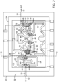
- FIG. 2 is a schematic top view of a TTD module 22 incorporated in the radar system or RF transmission system 10 of FIG. 1 , according to one embodiment of the invention.
- the TTD module 22 includes a micro-strip transmission line 30 or signal line patterned on a base substrate 56 to include four (4) sets of time delay stages 32, 34, 36, 38.
- Micro-strip transmission line 30 is formed using a deposition, patterning, and/or etching technique as known in the art.
- base substrate 56 is formed of fused silica, which provides reduced current leakage and improved switch channel isolation.
- base substrate 56 may be an insulating, semi-insulating material, or semi-conductive material such as, but not limited to glass, alumina, ceramic, LTCC, HTCC, quartz, polyimide, gallium arsenide, silicon, or germanium.
- base substrate 56 may be a semiconductor wafer processed to include switching elements or switches 44, 46 and micro-strip transmission line 30.
- Micro-strip transmission line 30 may be any conductive material such as, for example, copper, gold, a tungsten/nickel/gold stack, or another common packaging material. As shown, micro-strip transmission line 30 is patterned such that the delay stages 32, 34, 36, 38 are serially connected, with the first delay stage 32 coupled to an RF signal input 40 of the TTD module 22 and the fourth delay stage 38 coupled to the RF signal output 42 of the TTD module 22. Each of the delay stages 32, 34, 36, 38 includes an input electronic switching element 44 and an output electronic switching element 46 that are selectively controlled in either their on or off positions to insert a cumulative time delay in a transmission signal sent to the respective antenna element 14 ( FIG. 1 ), as described in additional detail below.
- elements 40 and 42 are described herein as input and output, respectively, it is contemplated that the functionality of elements 40, 42 might be reversed such that element 40 is an RF signal output and element 42 is an RF signal input.
- switching elements 44 and 46 function as respective "input” and “output” switching elements of respective delay lines 48, 50, 52, 54 when an RF signal travels through TTD module 22 from RF signal element 40 to RF signal element 42 and as “output” and “input” switching elements, respectively, when the signal travels in the reverse direction.
- the first delay stage 32 includes four micro-strip delay lines 48, 50, 52, 54 patterned on the base substrate 56 of the TTD module 22.
- Delay lines 48, 50, 52, 54 have different lengths that impart different time delays to the RF input signal.
- Delay line 48 has a length L1
- delay line 50 has a length L2
- delay line 52 has a length L3
- delay line 54 has a length L4, with L1 ⁇ L2 ⁇ L3 ⁇ L4.
- the phase of the transmission signal is shifted in proportion to the time delay imparted by the delay line 48, 50, 52, 54, with the longest delay line 54 imparting the greatest time delay.
- the second, third, and fourth delay stages 34, 36, 38 are formed in a similar manner as the first delay stage 32, with each delay stage 34, 36, 38 including four micro-strip delay lines 48-54 of varying lengths patterned on the base substrate 56. Line segments 58, 60, 62 interconnect the delay stages 32-38. Additional phase shift is imparted to the input signal by each subsequent delay stage 34-38 by selectively closing a given pair of switches 44, 46 on one of the four micro-strip delay lines 48-54 while the remaining pairs of switches are maintained in an open position a similar manner as described above.
- Switching devices 44, 46 are positioned on base substrate 56 at the terminal input and terminal output, respectively, of each micro-strip delay line 48-54.
- the micro-strip delay lines 48-54 of the first delay stage 32 and the third delay stage 36 are constructed having a star or fan out configuration and the micro-strip delay lines 48-54 of the second delay stage 34 and the fourth delay stage 38 are constructed having a linear configuration.
- the delay stages may be constructed having any number alternative configurations based on design specifications of a particular application.
- the TTD module 22 disclosed herein is designed as a 256 state beam former, with four (4) delay stages, and a 360 degree delay/phase-shift range. TTD module 22 is operable over the entire Ku-band or over a 10-15 GHz bandwidth. However, it is contemplated that the concepts disclosed herein may be extended to TTD modules having any number of delay stages, with the number of delay stages and the length of the individual delay lines within those stages determined based on the desired amount of delay and resulting beam steering resolution for a particular application. Likewise, while the dimensions of TTD module 22 disclosed herein are approximately 9mm by 7.5mm, a skilled artisan will recognize that the dimensions of TTD module may be altered based on the design specifications of a particular application.
- switches 44, 46 are provided as MEMS devices - such that the TTD module 22 may be referred to as an "RF MEMS transmission device.”
- the MEMS switches 44, 46 may be formed using a build-up technique involving multiple deposition, anodization, patterning, and etching steps.
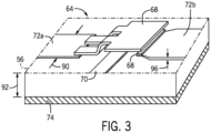
- MEMS switches 44, 46 have a construction similar to the MEMS switch 64 depicted in FIG. 3 , which is illustrated as an ohmic contact switch mechanism.
- MEMS switch 64 includes a contact 66 and a moveable element 68 such as for example, a cantilevered beam.
- the moveable element 68 can be supported by an anchor, which may be integrated with the moveable element 68 and serve to connect the moveable element 68 to an underlying support structure such as base substrate 56.
- the moveable element 68 is a cantilevered beam that includes two cantilever portions connected to a common beam portion.
- Contact 66, cantilevered beam 68, and electrode 70 are formed at least partially of at least one conductive material such as gold, gold alloy, nickel, nickel alloy, platinum, tantalum, and tungsten, as non-limiting examples.
- the switch 64 also includes an electrode or driving means 70 that effects a potential difference between the electrode 70 and the cantilevered beam 68.
- switch 44 As shown in FIG. 3 , the contact 66 and moveable element 68 of switch 44 are formed between two micro-strip lines 72a and 72b patterned on base substrate 56, with the electrode 70 positioned between micro-strip lines 72a and 72b.
- Switch 44 may be formed on base substrate 56 through a micro fabrication technique, such as, for example, vapor deposition, electroplating, photolithography, wet and dry etching, and the like, such that switch 44 constitutes a portion of a microelectromechanical device, nanoelectromechanical device, or MEMS. In such an embodiment, switch 44 is fabricating having features on the order of ones or tens of micrometers or nanometers.
- the electrode 70 of MEMS switch 64 When appropriately charged, the electrode 70 of MEMS switch 64 generates an electrostatic force that pulls the cantilevered beam 68 toward the electrode 70 and the contact 66.
- the electrode 70 thus acts as a gate with respect to the switch 44, causing the cantilevered moveable element 68 to move between a non-contacting or "open” position in which the moveable element 68 is separated from the contact 66 (shown in FIG. 4 ), and a contacting or “closed” position in which the moveable element 68 contacts and establishes electrical communication with the contact 66, thereby closing a circuit between micro-strip lines 72a and 72b.
- an embedded micro-strip configuration is provided with MEMS switch 64 (and overall in TTD module 22 of FIG. 2 ) by including a ground layer 74 below the base substrate 56 along with micro-strip lines 72a and 72b (and micro-strip transmission lines 30, FIG. 2 ) patterned on base substrate 56 - with the micro-strip lines and ground plane layer 74 interacting with each other to create an electromagnetic wave that travels through dielectric substrate 56 to create an RF signal. While a specific grounding configuration is illustrated in FIG.
- TTD module 22 may be fabricated having alternative strip-line and embedded micro-strip grounding configurations, such as, for example a grounded coplanar waveguide configuration wherein two ground lines (not shown) are provided coplanar to the micro-strip transmission line 30 on the base substrate 56.
- TTD module 22 is constructed with an inverted ground plane (not shown) that is positioned above the anchor 30 and base substrate 56.
- a given delay line such as delay line 48 of the third delay stage 36 for example, is activated by closing the input switch 44 and output switch 46 on the delay line 48 while maintaining the switches 44, 46 on delay lines 50-54 in an open position.
- the MEMS switches 44, 46 of TTD module 22 are controlled to move between their open and closed positions by applying a selective gate voltage to the electrode 70 of the MEMS switch 44, 46.
- This gate voltage is provided through gating lines (not shown) patterned on the base substrate 56, with the gating lines electrically coupling the MEMS switches 44, 46 to gate voltage sources or gate drivers (not shown) that receive power from power sources to establish a potential difference between the contact 66 and the cantilevered beam 68 of the MEMS switches 44, 46 when the switch is in the open position.
- TTD module 22 With regard to the operation of TTD module 22, it is recognized that ideal operation of the module would be at a characteristic impedance of 50 Ohms - which would typically match with a 50 Ohm source resistance and load resistance found in an RF transmission system. However, it is recognized that it may be difficult to achieve a characteristic impedance of 50 Ohms in TTD module 22 due to the small size of the RF MEMS devices 44, 46 and micro-strip transmission line 30 in the module. For example, characteristic impedance may be lowered in TTD module 22 by increasing a width of the micro-strip transmission line 30, but such altering would result in an increased size of the module.
- characteristic impedance may be lowered by reducing a thickness of the substrate 56, such as by forming the substrate with a thickness of 125 ⁇ m, but such thinning of the substrate 56 may lead to poorer yields during fabrication due to the fragility of the substrate and potential breakage thereof that might occur with such reduced thickness.
- embodiments of the invention are directed to an RF MEMS transmission device (such as TTD module 22) having a selectively increased characteristic impedance.
- the characteristic impedance in TTD module 22 is increased to a level of 150 Ohms, which minimizes the impact of resistive losses in the micro-strip transmission line 30 and MEMS switches 44, 46 and lowers RF insertion loss, so as enable passive beamformer assemblies and maintain good signal transmission.
- Block schematic diagrams of a prior art RF MEMS transmission system 76 and an RF MEMS transmission system 78 according to an embodiment of the invention are shown in FIGS. 4A and 4B , respectively.
- each of the RF MEMS transmission systems 76, 78 includes an RF source 80 and an RF load 82 (e.g., radiating antenna element) that have a characteristic impedance of 50 Ohms.
- the prior art RF MEMS transmission system 76 of FIG. 4A includes a 4-stage TTD module 84 having a characteristic impedance of 50 Ohms (based on the construction thereof, as will be explained in greater detail below), whereas the 4-stage TTD module 86 of FIG. 4B has an increased characteristic impedance of 150 Ohms (based on the construction thereof, as will be explained in greater detail below).
- impedance transformers 88 are provided at the input and output of TTD module 86 to account for differences in the characteristic impedance between the RF source80, the TTD module 86, and the RF load 82 - with the impedance transformers 88 increasing/decreasing the characteristic impedance as required to transition between these impedance values.
- Such impedance transformers 88 may be of a known construction and function to convert current at one voltage to the same waveform at another voltage, with a balun transformer being one possible device/component to perform the impedance transformation, for example.
- the impedance transformers 88 may be formed on the same substrate as the TTD module 86 to enable a 50 Ohm "part" to be created.
- impedance transformers 88 may be formed on base substrate 56 ( FIG. 2 ) of the TTD module 86 as part of the fabrication thereof, so as to be considered an integral part/component of the TTD module - with the TTD module 86 functioning as a 50 Ohm device.
- one or more of a width of the micro-strip transmission lines 30 and a thickness of the substrate 56 may be selectively controlled relative to one another during fabrication of the TTD module 22, 86.
- a width of the micro-strip transmission lines 72a, 72b, indicated at 90, and a thickness of the substrate 56, indicated at 92 are illustrated.
- varying a width 90 of the micro-strip transmission lines 72a, 72b (and of lines 30 generally, in FIG 2 ) alters the characteristic impedance in TTD module 22 - with a narrowing of the width 90 increasing the characteristic impedance.
- varying a thickness 92 of the substrate 56 alters the characteristic impedance in TTD module 22 - with a thickening of the substrate 56 increasing the characteristic impedance.
- Various combinations of substrate thickness 56 and micro-strip transmission line width 90 - when taken in combination with a length 94 and thickness 96 of the micro-strip transmission lines 72a, 72b and material properties of the substrate 56 and micro-strip transmission lines 72a, 72b (e.g., gallium arsenide (GaAs) substrate and copper lines) - are possible to achieve a desired characteristic impedance in TTD module 22 and examples of such combinations are provided here below in Table 1, with such thicknesses/widths being provided for a prior art 50 Ohm TTD module and for various 150 Ohm TTD modules, according to embodiments of the invention.
- Micro-Strip Width ( ⁇ m) Micro-Strip Thickness ( ⁇ m) Substrate Thickness ( ⁇ m) Characteristic Impedance (Ohms) Resistive Loss (dB/mm) Module #1 (Prior Art) 270 1 125 49.920 0.0118 Module #2 18 1 125 148.888 0.0417 Module #3 70 1 500 151.277 0.0121 Module #4 42 1 300 150.843 0.0193
- each of the TTD modules with a characteristic impedance of approximately 150 Ohms i.e., 150 +/- 0.0 to 1.3 Ohms
- the overall resistive loss in the TTD modules is dominated by the contact resistance of the MEMS switches 44, 46.
- the overall impact of resistive loss in the TTD module is relative to the characteristic impedance of the TTD module - with the impact of resistive loss decreasing as the characteristic impedance of the TTD module increases.
- impedance transformers 88 While it is recognized that the useage of impedance transformers 88 with the TTD module 86 (either positioned at inputs/outputs of the TTD module or formed on the same substrate as the TTD module, so as to be a part thereof) serves to reduce the bandwidth of the RF transmission system, this reduction does not have a negative impact on system operation. That is, as the antenna elements 14 in the radar system 10 ( FIG. 1 ) already limit the bandwidth of the system, the inclusion of impedance transformers 88 in the RF transmission system do not have any additional negative impact on the system bandwidth.
- embodiments of the invention thus provide an RF MEMS transmission device (such as a TTD module) having selectively increased characteristic impedance that: reduces insertion losses, improves yields of RF transmission lines in the system, and/or minimizes the planar space of the system.
- An increasing of the characteristic impedance can be achieved via a thickening of the substrate on which the micro-strip transmission lines are formed, such as to thicknesses of between 100-500 ⁇ m, with the thickening of the substrate also providing greater stability during fabrication thereof so as to decrease the risk of wafer breakage and improve line yield (e.g., increase from 20% yield to 80% yield).
- An increasing of the characteristic impedance can also be achieved via a narrowing of the micro-strip transmission lines, such as to a width of between 20-200 ⁇ m, with the narrowing of the micro-strip transmission lines also allowing for a decrease in the planar space of the RF transmission system.
- the thickening of the substrate and/or the narrowing of the micro-strip transmission lines can be selectively optimized according to a selection process so as to achieve a desired increased impedance - such as 150 Ohms, for example.
- Impedance transformers can be employed to perform impedance matching between the high impedance RF MEMS transmission system and the lower impedances of the RF source and RF load, with it being recognized that the impedance transformers should not have an adverse affect on the system bandwidth based on antenna elements in the system already limiting the bandwidth of the system.
- an RF transmission system includes an RF source that provides an RF input and one or more RF MEMS transmission devices coupled to the RF source to receive the RF input therefrom and generate output signals for transmission to an RF load.
- Each of the one or more RF MEMS transmission devices comprises a substrate, a conducting line formed on the substrate to provide signal transmission paths between a signal input of the RF MEMS transmission device and a signal output of the RF MEMS transmission device, and a plurality of switching elements positioned along the conducting line and selectively controllable to define the signal transmission paths between the signal input and the signal output.
- Each of the RF source and the RF load has a first characteristic impedance and the one or more RF MEMS transmission devices have a second characteristic impedance that is greater than the first characteristic impedance.
- a method of manufacturing an RF MEMS transmission device includes forming a substrate, forming a signal line on a top surface of the substrate that includes plurality of line portions, and coupling a MEMS switching device to the signal line, the MEMS switching device operable in a closed position and an open position to selectively couple and decouple respective line portions of the signal line to transmit an RF signal therethrough.
- Forming the substrate and the signal line comprises selectively controlling a thickness of the substrate and a width of the signal line relative to one another such that, when taken in combination with a length and thickness of the signal line and material properties of the substrate and signal line, a characteristic impedance of the RF MEMS transmission device is higher than a 50 Ohm characteristic impedance of an RF source and an RF load to which the RF MEMS transmission device is connected.
- an RF MEMS transmission device includes a substrate having a thickness, a plurality of MEMS devices disposed on a top surface of the substrate, and conductive signal lines formed on the top surface of the substrate, the conductive signal lines each having a length, width, and thickness.
- the thickness of the substrate and the width of the conductive signal lines is such that, when taken in combination with others of the thickness of the substrate and the length, width, and thickness of the conductive signal lines, a characteristic impedance of the RF MEMS transmission device is approximately 150 Ohms.
Landscapes
- Engineering & Computer Science (AREA)
- Computer Hardware Design (AREA)
- Microelectronics & Electronic Packaging (AREA)
- Waveguide Switches, Polarizers, And Phase Shifters (AREA)
- Variable-Direction Aerials And Aerial Arrays (AREA)
Claims (11)
- Radiofrequenz-, RF-, Übertragungssystem (10), umfassend:eine RF-Quelle (16), die eine RF-Eingabe bereitstellt;eine RF-Last, eine oder mehrere RF- mikroelektromechanische System-, MEMS-, Übertragungsvorrichtungen (22), die mit der RF-Quelle (16) gekoppelt sind, um die RF-Eingabe von derselben zu empfangen und Ausgabesignale zur Übertragung an eine RF-Last zu erzeugen, wobei jede der einen oder der mehreren RF-MEMS-Übertragungsvorrichtungen (22) Folgendes umfasst:ein Substrat (56);eine leitfähige Signalleitung (30), die auf dem Substrat (56) ausgebildet ist, um Signalübertragungspfade zwischen einer Signaleingabe (40) der RF-MEMS-Übertragungsvorrichtung (22) und einer Signalausgabe (42) der RF-MEMS-Übertragungsvorrichtung (22) bereitzustellen; undeine Vielzahl von Schaltelementen (44, 46), die entlang der leitfähigen Signalleitung (30) positioniert und selektiv steuerbar sind, um die Signalübertragungspfade zwischen der Signaleingabe (40) und der Signalausgabe (42) zu definieren;dadurch gekennzeichnet, dass jedes aus der RF-Quelle (16) und die RF-Last eine erste kennzeichnende Impedanz aufweist und die eine oder die mehreren RF-MEMS-Übertragungsvorrichtungen (22) eine zweite kennzeichnende Impedanz aufweisen, die größer ist als die erste kennzeichnende Impedanz,wobei die erste kennzeichnende Impedanz der RF-Quelle (16) und der RF-Last etwa 50 Ohm beträgt und die zweite kennzeichnende Impedanz der einen oder der mehreren RF-MEMS-Übertragungsvorrichtungen (22) etwa 150 Ohm beträgt.
- RF-Übertragungssystem (10) nach Anspruch 1, ferner umfassend:einen ersten Impedanztransformator, der zwischen der RF-Quelle (16) und der einen oder den mehreren RF-MEMS-Übertragungsvorrichtungen (22) positioniert ist, um die erste kennzeichnende Impedanz der RF-Quelle (16) auf die zweite kennzeichnende Impedanz der einen oder der mehreren RF-MEMS-Übertragungsvorrichtungen (22) zu erhöhen und an diese anzupassen; undeinen zweiten Impedanztransformator, der zwischen der einen oder den mehreren RF-MEMS-Übertragungsvorrichtungen (22) und der RF-Last positioniert ist, um die zweite kennzeichnende Impedanz der einen oder der mehreren RF-MEMS-Übertragungsvorrichtungen (22) auf die erste kennzeichnende Impedanz der RF-Last zu verringern und an diese anzupassen.
- RF-Übertragungssystem (10) nach Anspruch 2, wobei der erste und der zweite Impedanztransformator als separate Komponenten von den RF-MEMS-Übertragungsvorrichtungen (22) bereitgestellt werden oder auf dem Substrat (56) der RF-MEMS-Übertragungsvorrichtungen (22) ausgebildet sind, sodass sie Teil der RF-MEMS-Übertragungsvorrichtungen (22) sind.
- RF-Übertragungssystem (10) nach Anspruch 1, wobei das Substrat (56) eine Dicke aufweist und die leitfähigen Signalleitungen (30) jeweils eine Länge, Breite, und Dicke aufweisen, und wobei mindestens eines aus der Dicke des Substrats (56) und der Breite der leitfähigen Signalleitungen (30) derart ist, dass, wenn es mit anderen aus der Dicke des Substrats (56) und der Länge, Breite und Dicke der leitfähigen Signalleitungen (30) kombiniert wird, die kennzeichnende Impedanz der RF-MEMS-Übertragungsvorrichtung (22) etwa 150 Ohm beträgt.
- RF-Übertragungssystem (10) nach Anspruch 4, wobei die Dicke des Substrats (56) zwischen 100 Mikrometer und 500 Mikrometer beträgt.
- RF-Übertragungssystem (10) nach Anspruch 4, wobei die Breite der leitfähigen Signalleitungen (30) zwischen 20 Mikrometer und 200 Mikrometer beträgt.
- RF-Übertragungssystem (10) nach Anspruch 1,a. wobei der Betrieb der einen oder mehreren RF-MEMS-Übertragungsvorrichtungen (22) an der zweiten kennzeichnenden Impedanz Einfügeverluste in dieselbe im Vergleich zu dem Betrieb an der ersten Impedanz verringert, oderb. wobei jede der einen oder der mehreren RF-MEMS-Übertragungsvorrichtungen (22) ein Echtzeitverzögerungs-,TTD-, Modul umfasst, wobei die Vielzahl von Schaltelementen (44, 46) Folgendes umfasst: ein Eingabeschaltelement (44), das an einem ersten Ende jeder der Vielzahl von Zeitverzögerungsleitungen positioniert ist; und ein Ausgabeschaltelement (46), das an einem zweiten Ende jeder der Vielzahl von Zeitverzögerungsleitungen positioniert ist; wobei das Eingabeschaltelement (44) und das Ausgabeschaltelement (46) selektiv zwischen einem leitenden und einem nicht leitenden Zustand steuerbar sind, um Signalübertragungspfade mit variierenden Längen zwischen der Signaleingabe (40) und der Signalausgabe (42) auszubilden oderc. wobei das Substrat (56) eines aus Glas, Aluminium, Keramik, LTCC, HTCC, Quarz, Polyimid, Galliumarsenid, Silizium oder Germanium umfasst oderd. ferner umfassend eine Masseebene, die an dem Substrat (56) befestigt ist, wobei die Masseebene und die leitfähige Signalleitung (30) eine RF-Übertragungsleitung für die RF-MEMS-Übertragungsvorrichtung (22) ausbilden.
- Verfahren zum Herstellen einer Radiofrequenz-, RF-, mikroelektromechanischen System-, MEMS-, Übertragungsvorrichtung (22), umfassend:Ausbilden eines Substrats (56);Ausbilden einer leitfähigen Signalleitung (30) auf einer Oberseite des Substrats (56), wobei die leitfähige Signalleitung (30) eine Vielzahl von Leitungsabschnitten umfasst;Koppeln einer MEMS-Schaltvorrichtung (44, 46) mit der leitfähigen Signalleitung (30), wobei die MEMS-Schaltvorrichtung (44, 46) betriebsfähig in einer geschlossenen Position und einer offenen Position ist, um selektiv die jeweiligen Leitungsabschnitte der leitfähigen Signalleitung (30) zu koppeln und zu entkoppeln, um durch dieselben ein RF-Signal zu übertragen;dadurch gekennzeichnet, dass das Ausbilden des Substrats (56) und der leitfähigen Signalleitung (30) das selektive Steuern einer Dicke des Substrats (56) und einer Breite der Signalleitung relativ zu einer anderen umfasst, sodass, wenn sie mit einer Länge und Dicke der leitfähigen Signalleitung (30) und Materialeigenschaften des Substrats (56) und der leitfähigen Signalleitung (30) kombiniert werden, eine zweite kennzeichnende Impedanz der RF-MEMS-Übertragungsvorrichtung (22) höher ist als eine erste kennzeichnende Impedanz einer RF-Quelle (16) und einer RF-Last, mit der die RF-MEMS-Übertragungsvorrichtung (22) verbunden ist, wobei die erste kennzeichnende Impedanz der RF-Quelle (16) und der RF-Last etwa 50 Ohm beträgt, unddie Dicke des Substrats (56) und die Breite der leitfähigen Signalleitung (30) selektiv gesteuert sind, um eine zweite kennzeichnende Impedanz in der RF-MEMS-Übertragungsvorrichtung (22) von etwa 150 Ohm bereitzustellen.
- Verfahren nach Anspruch 8, ferner umfassend das Bereitstellen eines Impedanztransformators an jeder aus einer Signaleingabe (40) und einer Signalausgabe (42) der RF-MEMS-Übertragungsvorrichtung (22), sodass eine Impedanz zur Anpassung zwischen den 50 Ohm der RF-Quelle (16) und der RF-Last und den etwa 150 Ohm der RF-MEMS-Übertragungsvorrichtung (22) bereitgestellt wird, wobei der Impedanztransformator auf dem Substrat (56) der RF-MEMS-Übertragungsvorrichtung (22) ausgebildet ist oder als separate und eigenständige Komponenten bereitgestellt wird.
- Verfahren nach Anspruch 9, wobei die Vielzahl von Leitungsabschnitten der leitfähigen Signalleitung (30) eine Vielzahl von Verzögerungsleitungen umfasst, die alternative Pfade zwischen der Signaleingabe (40) und der Signalausgabe (42) der RF-MEMS-Übertragungsvorrichtung (22) so definieren, dass ein Echtzeitverzögerungs-, TTD-, Modul ausgebildet wird.
- Verfahren nach Anspruch 8, wobei das selektive Steuern der Dicke des Substrats (56) und der Breite der leitfähigen Signalleitung (30) das Ausbilden des Substrats (56) umfasst, um eine Dicke zwischen 100 Mikrometer und 500 Mikrometer aufzuweisen, und das Ausbilden der leitfähigen Signalleitung (30), um eine Breite zwischen 20 Mikrometer und 200 Mikrometer aufzuweisen.
Applications Claiming Priority (2)
| Application Number | Priority Date | Filing Date | Title |
|---|---|---|---|
| US15/786,696 US10326200B2 (en) | 2017-10-18 | 2017-10-18 | High impedance RF MEMS transmission devices and method of making the same |
| PCT/US2018/048090 WO2019078952A1 (en) | 2017-10-18 | 2018-08-27 | HIGH IMPEDANCE RF MEMS TRANSMISSION DEVICES AND METHOD FOR MANUFACTURING SAME |
Publications (4)
| Publication Number | Publication Date |
|---|---|
| EP3698429A1 EP3698429A1 (de) | 2020-08-26 |
| EP3698429A4 EP3698429A4 (de) | 2021-07-07 |
| EP3698429B1 true EP3698429B1 (de) | 2024-10-02 |
| EP3698429B8 EP3698429B8 (de) | 2024-11-06 |
Family
ID=66097537
Family Applications (1)
| Application Number | Title | Priority Date | Filing Date |
|---|---|---|---|
| EP18869267.7A Active EP3698429B8 (de) | 2017-10-18 | 2018-08-27 | Hf-mems-übertragungsvorrichtungen mit hoher impedanz und verfahren zu ihrer herstellung |
Country Status (6)
| Country | Link |
|---|---|
| US (1) | US10326200B2 (de) |
| EP (1) | EP3698429B8 (de) |
| JP (1) | JP7217748B2 (de) |
| KR (1) | KR102562909B1 (de) |
| CN (1) | CN111226347B (de) |
| WO (1) | WO2019078952A1 (de) |
Families Citing this family (6)
| Publication number | Priority date | Publication date | Assignee | Title |
|---|---|---|---|---|
| CN110127593A (zh) * | 2019-04-28 | 2019-08-16 | 中北大学 | 一种星型单刀四掷射频开关 |
| CN110706981A (zh) * | 2019-10-21 | 2020-01-17 | 中北大学 | 一种结合单刀四掷开关的射频mems四路蛇形延时器 |
| US11180366B2 (en) | 2020-03-23 | 2021-11-23 | General Electric Company | Methods for forming a MEMS device layer on an active device layer and devices formed thereby |
| CN113782972A (zh) * | 2021-07-30 | 2021-12-10 | 北京邮电大学 | 一种多波段可重构微带天线 |
| DE102021212216A1 (de) | 2021-10-29 | 2023-05-04 | Robert Bosch Gesellschaft mit beschränkter Haftung | Hochfrequenz-Filtervorrichtung, Hochfrequenzmodul und Hochfrequenz-Filterverfahren |
| US12365579B2 (en) * | 2021-12-29 | 2025-07-22 | Menlo Microsystems, Inc. | Distributed MEMS switch array design with multiple input/output ports |
Family Cites Families (22)
| Publication number | Priority date | Publication date | Assignee | Title |
|---|---|---|---|---|
| US4649393A (en) * | 1984-02-17 | 1987-03-10 | The United States Of America As Represented By The Secretary Of The Army | Phased array antennas with binary phase shifters |
| US5541614A (en) * | 1995-04-04 | 1996-07-30 | Hughes Aircraft Company | Smart antenna system using microelectromechanically tunable dipole antennas and photonic bandgap materials |
| US5757319A (en) | 1996-10-29 | 1998-05-26 | Hughes Electronics Corporation | Ultrabroadband, adaptive phased array antenna systems using microelectromechanical electromagnetic components |
| US6191735B1 (en) * | 1997-07-28 | 2001-02-20 | Itt Manufacturing Enterprises, Inc. | Time delay apparatus using monolithic microwave integrated circuit |
| US6281838B1 (en) * | 1999-04-30 | 2001-08-28 | Rockwell Science Center, Llc | Base-3 switched-line phase shifter using micro electro mechanical (MEMS) technology |
| US6307519B1 (en) | 1999-12-23 | 2001-10-23 | Hughes Electronics Corporation | Multiband antenna system using RF micro-electro-mechanical switches, method for transmitting multiband signals, and signal produced therefrom |
| US6741207B1 (en) * | 2000-06-30 | 2004-05-25 | Raytheon Company | Multi-bit phase shifters using MEM RF switches |
| US6535091B2 (en) | 2000-11-07 | 2003-03-18 | Sarnoff Corporation | Microelectronic mechanical systems (MEMS) switch and method of fabrication |
| US6650291B1 (en) | 2002-05-08 | 2003-11-18 | Rockwell Collins, Inc. | Multiband phased array antenna utilizing a unit cell |
| US7253699B2 (en) | 2003-05-12 | 2007-08-07 | Hrl Laboratories, Llc | RF MEMS switch with integrated impedance matching structure |
| US7068220B2 (en) | 2003-09-29 | 2006-06-27 | Rockwell Scientific Licensing, Llc | Low loss RF phase shifter with flip-chip mounted MEMS interconnection |
| US7157993B2 (en) * | 2003-09-30 | 2007-01-02 | Rockwell Scientific Licensing, Llc | 1:N MEM switch module |
| US7724189B2 (en) * | 2004-11-24 | 2010-05-25 | Agilent Technologies, Inc. | Broadband binary phased antenna |
| US7570133B1 (en) * | 2006-03-23 | 2009-08-04 | Lockheed Martin Corporation | Wideband passive amplitude compensated time delay module |
| US20090027268A1 (en) | 2006-08-15 | 2009-01-29 | Coward James F | Multi Beam Photonic Beamformer |
| DE102007027155A1 (de) | 2007-04-03 | 2008-10-23 | Rohde & Schwarz Gmbh & Co. Kg | Wellenleiter-System mit differenziellem Wellenleiter |
| CN101202369B (zh) * | 2007-12-11 | 2011-12-07 | 中国电子科技集团公司第五十五研究所 | 一种小型化mems开关线移相器 |
| JP5344736B2 (ja) * | 2008-02-20 | 2013-11-20 | 太陽誘電株式会社 | 基材、通信モジュール、および通信装置 |
| CN101834339A (zh) * | 2010-04-23 | 2010-09-15 | 电子科技大学 | 一种基片集成波导结构延迟线 |
| WO2014142885A1 (en) | 2013-03-14 | 2014-09-18 | Viasat, Inc. | Wideband true time delay circuits for antenna architectures |
| EP3422464B1 (de) * | 2015-12-29 | 2021-02-24 | Synergy Microwave Corporation | Mikrowellen-mems-phasenschieber |
| US10594030B2 (en) * | 2017-02-01 | 2020-03-17 | General Electric Company | True time delay module and beam former having plural delay lines selectively connected by plural switching elements including one or more intermediate switching element |
-
2017
- 2017-10-18 US US15/786,696 patent/US10326200B2/en active Active
-
2018
- 2018-08-27 JP JP2020521589A patent/JP7217748B2/ja active Active
- 2018-08-27 KR KR1020207013786A patent/KR102562909B1/ko active Active
- 2018-08-27 CN CN201880066919.7A patent/CN111226347B/zh active Active
- 2018-08-27 WO PCT/US2018/048090 patent/WO2019078952A1/en not_active Ceased
- 2018-08-27 EP EP18869267.7A patent/EP3698429B8/de active Active
Also Published As
| Publication number | Publication date |
|---|---|
| CN111226347B (zh) | 2021-05-07 |
| WO2019078952A1 (en) | 2019-04-25 |
| EP3698429A4 (de) | 2021-07-07 |
| US10326200B2 (en) | 2019-06-18 |
| CN111226347A (zh) | 2020-06-02 |
| JP7217748B2 (ja) | 2023-02-03 |
| EP3698429A1 (de) | 2020-08-26 |
| JP2021500793A (ja) | 2021-01-07 |
| KR102562909B1 (ko) | 2023-08-02 |
| US20190115659A1 (en) | 2019-04-18 |
| EP3698429B8 (de) | 2024-11-06 |
| KR20200059304A (ko) | 2020-05-28 |
Similar Documents
| Publication | Publication Date | Title |
|---|---|---|
| US10326200B2 (en) | High impedance RF MEMS transmission devices and method of making the same | |
| US6624720B1 (en) | Micro electro-mechanical system (MEMS) transfer switch for wideband device | |
| US10594030B2 (en) | True time delay module and beam former having plural delay lines selectively connected by plural switching elements including one or more intermediate switching element | |
| JP7212684B2 (ja) | 実時間遅延ビームフォーマおよび動作方法 | |
| US9048053B2 (en) | Electrostatic micro relay and manufacturing method for the same | |
| CN1938807B (zh) | 可弯折接触开关 | |
| EP1690319B1 (de) | Kompaktes breitbandiges integriertes aktives modul für radar- und kommunikationssysteme | |
| CA2540334C (en) | 1:n mem switch module | |
| US8115577B2 (en) | Electromechanical switch, filter using the same, and communication apparatus | |
| US20090272635A1 (en) | Mems switch provided with movable electrode member supported through springs on substrate having bump | |
| CN104183425B (zh) | 一种射频mems单刀双掷开关 | |
| Simon et al. | Designing a novel RF MEMS switch for broadband power applications | |
| CN119651142B (zh) | 基于rf mems开关控制的单极子方向图可重构天线 | |
| US20240087828A1 (en) | Mems switch for rf applications | |
| KR100812514B1 (ko) | 레이더 및 통신 시스템용의 콤팩트한 광대역 집적 능동모듈 | |
| CN120545695A (zh) | 一种基于rf-mems开关太赫兹方向图可重构天线 | |
| JP2008131096A (ja) | 移相器及びアンテナ装置 | |
| CN117293541A (zh) | 基于单刀三掷mems开关的ka波段方向图可重构天线 | |
| Le Garrec et al. | Cpw-fed slot microstrip mems-based reconfigurable arrays | |
| KR20020078809A (ko) | 수평 동작형 MEMs 스위치 | |
| Manimegalai et al. | MEMS-based switchable coplanar-waveguide-fed slot antenna | |
| JP2007035328A (ja) | マイクロマシンスイッチ及び電子機器 |
Legal Events
| Date | Code | Title | Description |
|---|---|---|---|
| STAA | Information on the status of an ep patent application or granted ep patent |
Free format text: STATUS: THE INTERNATIONAL PUBLICATION HAS BEEN MADE |
|
| PUAI | Public reference made under article 153(3) epc to a published international application that has entered the european phase |
Free format text: ORIGINAL CODE: 0009012 |
|
| STAA | Information on the status of an ep patent application or granted ep patent |
Free format text: STATUS: REQUEST FOR EXAMINATION WAS MADE |
|
| 17P | Request for examination filed |
Effective date: 20200515 |
|
| AK | Designated contracting states |
Kind code of ref document: A1 Designated state(s): AL AT BE BG CH CY CZ DE DK EE ES FI FR GB GR HR HU IE IS IT LI LT LU LV MC MK MT NL NO PL PT RO RS SE SI SK SM TR |
|
| AX | Request for extension of the european patent |
Extension state: BA ME |
|
| DAV | Request for validation of the european patent (deleted) | ||
| DAX | Request for extension of the european patent (deleted) | ||
| REG | Reference to a national code |
Ref country code: DE Ref legal event code: R079 Free format text: PREVIOUS MAIN CLASS: H01P0003080000 Ipc: H01P0001120000 Ref country code: DE Ref legal event code: R079 Ref document number: 602018075058 Country of ref document: DE Free format text: PREVIOUS MAIN CLASS: H01P0003080000 Ipc: H01P0001120000 |
|
| A4 | Supplementary search report drawn up and despatched |
Effective date: 20210607 |
|
| RIC1 | Information provided on ipc code assigned before grant |
Ipc: H01P 1/12 20060101AFI20210531BHEP Ipc: H01P 1/18 20060101ALI20210531BHEP Ipc: H01P 5/02 20060101ALI20210531BHEP Ipc: H01H 1/00 20060101ALI20210531BHEP Ipc: H01H 59/00 20060101ALI20210531BHEP Ipc: H01Q 3/26 20060101ALI20210531BHEP |
|
| STAA | Information on the status of an ep patent application or granted ep patent |
Free format text: STATUS: EXAMINATION IS IN PROGRESS |
|
| 17Q | First examination report despatched |
Effective date: 20230616 |
|
| GRAP | Despatch of communication of intention to grant a patent |
Free format text: ORIGINAL CODE: EPIDOSNIGR1 |
|
| STAA | Information on the status of an ep patent application or granted ep patent |
Free format text: STATUS: GRANT OF PATENT IS INTENDED |
|
| INTG | Intention to grant announced |
Effective date: 20240513 |
|
| GRAS | Grant fee paid |
Free format text: ORIGINAL CODE: EPIDOSNIGR3 |
|
| GRAA | (expected) grant |
Free format text: ORIGINAL CODE: 0009210 |
|
| STAA | Information on the status of an ep patent application or granted ep patent |
Free format text: STATUS: THE PATENT HAS BEEN GRANTED |
|
| AK | Designated contracting states |
Kind code of ref document: B1 Designated state(s): AL AT BE BG CH CY CZ DE DK EE ES FI FR GB GR HR HU IE IS IT LI LT LU LV MC MK MT NL NO PL PT RO RS SE SI SK SM TR |
|
| REG | Reference to a national code |
Ref country code: GB Ref legal event code: FG4D |
|
| REG | Reference to a national code |
Ref country code: DE Ref legal event code: R081 Ref document number: 602018075058 Country of ref document: DE Owner name: GE INTELLECTUAL PROPERTY LICENSING, LLC, NISKA, US Free format text: FORMER OWNER: GENERAL ELECTRIC COMPANY, SCHENECTADY, NY, US |
|
| REG | Reference to a national code |
Ref country code: CH Ref legal event code: PK Free format text: BERICHTIGUNG B8 Ref country code: CH Ref legal event code: EP |
|
| RAP2 | Party data changed (patent owner data changed or rights of a patent transferred) |
Owner name: GE INTELLECTUAL PROPERTY LICENSING, LLC |
|
| REG | Reference to a national code |
Ref country code: IE Ref legal event code: FG4D |
|
| REG | Reference to a national code |
Ref country code: DE Ref legal event code: R096 Ref document number: 602018075058 Country of ref document: DE |
|
| REG | Reference to a national code |
Ref country code: LT Ref legal event code: MG9D |
|
| REG | Reference to a national code |
Ref country code: NL Ref legal event code: MP Effective date: 20241002 |
|
| REG | Reference to a national code |
Ref country code: AT Ref legal event code: MK05 Ref document number: 1729135 Country of ref document: AT Kind code of ref document: T Effective date: 20241002 |
|
| PG25 | Lapsed in a contracting state [announced via postgrant information from national office to epo] |
Ref country code: NL Free format text: LAPSE BECAUSE OF FAILURE TO SUBMIT A TRANSLATION OF THE DESCRIPTION OR TO PAY THE FEE WITHIN THE PRESCRIBED TIME-LIMIT Effective date: 20241002 |
|
| PG25 | Lapsed in a contracting state [announced via postgrant information from national office to epo] |
Ref country code: NL Free format text: LAPSE BECAUSE OF FAILURE TO SUBMIT A TRANSLATION OF THE DESCRIPTION OR TO PAY THE FEE WITHIN THE PRESCRIBED TIME-LIMIT Effective date: 20241002 |
|
| PG25 | Lapsed in a contracting state [announced via postgrant information from national office to epo] |
Ref country code: HR Free format text: LAPSE BECAUSE OF FAILURE TO SUBMIT A TRANSLATION OF THE DESCRIPTION OR TO PAY THE FEE WITHIN THE PRESCRIBED TIME-LIMIT Effective date: 20241002 Ref country code: PT Free format text: LAPSE BECAUSE OF FAILURE TO SUBMIT A TRANSLATION OF THE DESCRIPTION OR TO PAY THE FEE WITHIN THE PRESCRIBED TIME-LIMIT Effective date: 20250203 Ref country code: IS Free format text: LAPSE BECAUSE OF FAILURE TO SUBMIT A TRANSLATION OF THE DESCRIPTION OR TO PAY THE FEE WITHIN THE PRESCRIBED TIME-LIMIT Effective date: 20250202 |
|
| PG25 | Lapsed in a contracting state [announced via postgrant information from national office to epo] |
Ref country code: FI Free format text: LAPSE BECAUSE OF FAILURE TO SUBMIT A TRANSLATION OF THE DESCRIPTION OR TO PAY THE FEE WITHIN THE PRESCRIBED TIME-LIMIT Effective date: 20241002 |
|
| PG25 | Lapsed in a contracting state [announced via postgrant information from national office to epo] |
Ref country code: BG Free format text: LAPSE BECAUSE OF FAILURE TO SUBMIT A TRANSLATION OF THE DESCRIPTION OR TO PAY THE FEE WITHIN THE PRESCRIBED TIME-LIMIT Effective date: 20241002 |
|
| PG25 | Lapsed in a contracting state [announced via postgrant information from national office to epo] |
Ref country code: ES Free format text: LAPSE BECAUSE OF FAILURE TO SUBMIT A TRANSLATION OF THE DESCRIPTION OR TO PAY THE FEE WITHIN THE PRESCRIBED TIME-LIMIT Effective date: 20241002 |
|
| PG25 | Lapsed in a contracting state [announced via postgrant information from national office to epo] |
Ref country code: NO Free format text: LAPSE BECAUSE OF FAILURE TO SUBMIT A TRANSLATION OF THE DESCRIPTION OR TO PAY THE FEE WITHIN THE PRESCRIBED TIME-LIMIT Effective date: 20250102 |
|
| PG25 | Lapsed in a contracting state [announced via postgrant information from national office to epo] |
Ref country code: AT Free format text: LAPSE BECAUSE OF FAILURE TO SUBMIT A TRANSLATION OF THE DESCRIPTION OR TO PAY THE FEE WITHIN THE PRESCRIBED TIME-LIMIT Effective date: 20241002 Ref country code: LV Free format text: LAPSE BECAUSE OF FAILURE TO SUBMIT A TRANSLATION OF THE DESCRIPTION OR TO PAY THE FEE WITHIN THE PRESCRIBED TIME-LIMIT Effective date: 20241002 Ref country code: GR Free format text: LAPSE BECAUSE OF FAILURE TO SUBMIT A TRANSLATION OF THE DESCRIPTION OR TO PAY THE FEE WITHIN THE PRESCRIBED TIME-LIMIT Effective date: 20250103 |
|
| PG25 | Lapsed in a contracting state [announced via postgrant information from national office to epo] |
Ref country code: CZ Free format text: LAPSE BECAUSE OF FAILURE TO SUBMIT A TRANSLATION OF THE DESCRIPTION OR TO PAY THE FEE WITHIN THE PRESCRIBED TIME-LIMIT Effective date: 20241002 Ref country code: PL Free format text: LAPSE BECAUSE OF FAILURE TO SUBMIT A TRANSLATION OF THE DESCRIPTION OR TO PAY THE FEE WITHIN THE PRESCRIBED TIME-LIMIT Effective date: 20241002 |
|
| PG25 | Lapsed in a contracting state [announced via postgrant information from national office to epo] |
Ref country code: RS Free format text: LAPSE BECAUSE OF FAILURE TO SUBMIT A TRANSLATION OF THE DESCRIPTION OR TO PAY THE FEE WITHIN THE PRESCRIBED TIME-LIMIT Effective date: 20250102 |
|
| PG25 | Lapsed in a contracting state [announced via postgrant information from national office to epo] |
Ref country code: SM Free format text: LAPSE BECAUSE OF FAILURE TO SUBMIT A TRANSLATION OF THE DESCRIPTION OR TO PAY THE FEE WITHIN THE PRESCRIBED TIME-LIMIT Effective date: 20241002 |
|
| REG | Reference to a national code |
Ref country code: DE Ref legal event code: R097 Ref document number: 602018075058 Country of ref document: DE |
|
| PG25 | Lapsed in a contracting state [announced via postgrant information from national office to epo] |
Ref country code: DK Free format text: LAPSE BECAUSE OF FAILURE TO SUBMIT A TRANSLATION OF THE DESCRIPTION OR TO PAY THE FEE WITHIN THE PRESCRIBED TIME-LIMIT Effective date: 20241002 |
|
| PG25 | Lapsed in a contracting state [announced via postgrant information from national office to epo] |
Ref country code: RO Free format text: LAPSE BECAUSE OF FAILURE TO SUBMIT A TRANSLATION OF THE DESCRIPTION OR TO PAY THE FEE WITHIN THE PRESCRIBED TIME-LIMIT Effective date: 20241002 |
|
| PG25 | Lapsed in a contracting state [announced via postgrant information from national office to epo] |
Ref country code: SK Free format text: LAPSE BECAUSE OF FAILURE TO SUBMIT A TRANSLATION OF THE DESCRIPTION OR TO PAY THE FEE WITHIN THE PRESCRIBED TIME-LIMIT Effective date: 20241002 |
|
| PG25 | Lapsed in a contracting state [announced via postgrant information from national office to epo] |
Ref country code: IT Free format text: LAPSE BECAUSE OF FAILURE TO SUBMIT A TRANSLATION OF THE DESCRIPTION OR TO PAY THE FEE WITHIN THE PRESCRIBED TIME-LIMIT Effective date: 20241002 |
|
| PLBE | No opposition filed within time limit |
Free format text: ORIGINAL CODE: 0009261 |
|
| STAA | Information on the status of an ep patent application or granted ep patent |
Free format text: STATUS: NO OPPOSITION FILED WITHIN TIME LIMIT |
|
| PG25 | Lapsed in a contracting state [announced via postgrant information from national office to epo] |
Ref country code: SE Free format text: LAPSE BECAUSE OF FAILURE TO SUBMIT A TRANSLATION OF THE DESCRIPTION OR TO PAY THE FEE WITHIN THE PRESCRIBED TIME-LIMIT Effective date: 20241002 |
|
| 26N | No opposition filed |
Effective date: 20250703 |
|
| PGFP | Annual fee paid to national office [announced via postgrant information from national office to epo] |
Ref country code: DE Payment date: 20250827 Year of fee payment: 8 |
|
| PGFP | Annual fee paid to national office [announced via postgrant information from national office to epo] |
Ref country code: GB Payment date: 20250827 Year of fee payment: 8 |
|
| PGFP | Annual fee paid to national office [announced via postgrant information from national office to epo] |
Ref country code: FR Payment date: 20250825 Year of fee payment: 8 |
|
| REG | Reference to a national code |
Ref country code: CH Ref legal event code: H13 Free format text: ST27 STATUS EVENT CODE: U-0-0-H10-H13 (AS PROVIDED BY THE NATIONAL OFFICE) Effective date: 20260324 |
|
| PG25 | Lapsed in a contracting state [announced via postgrant information from national office to epo] |
Ref country code: MC Free format text: LAPSE BECAUSE OF FAILURE TO SUBMIT A TRANSLATION OF THE DESCRIPTION OR TO PAY THE FEE WITHIN THE PRESCRIBED TIME-LIMIT Effective date: 20241002 |
|
| PG25 | Lapsed in a contracting state [announced via postgrant information from national office to epo] |
Ref country code: LU Free format text: LAPSE BECAUSE OF NON-PAYMENT OF DUE FEES Effective date: 20250827 |
|
| PG25 | Lapsed in a contracting state [announced via postgrant information from national office to epo] |
Ref country code: CH Free format text: LAPSE BECAUSE OF NON-PAYMENT OF DUE FEES Effective date: 20250831 |