EP3697028B1 - Method and device for signal conversion, home bus system (hbs) circuit, and user equipment - Google Patents
Method and device for signal conversion, home bus system (hbs) circuit, and user equipment Download PDFInfo
- Publication number
- EP3697028B1 EP3697028B1 EP18865821.5A EP18865821A EP3697028B1 EP 3697028 B1 EP3697028 B1 EP 3697028B1 EP 18865821 A EP18865821 A EP 18865821A EP 3697028 B1 EP3697028 B1 EP 3697028B1
- Authority
- EP
- European Patent Office
- Prior art keywords
- signal
- hbs
- spi
- communication
- uart
- Prior art date
- Legal status (The legal status is an assumption and is not a legal conclusion. Google has not performed a legal analysis and makes no representation as to the accuracy of the status listed.)
- Active
Links
Images




Classifications
-
- G—PHYSICS
- G06—COMPUTING OR CALCULATING; COUNTING
- G06F—ELECTRIC DIGITAL DATA PROCESSING
- G06F13/00—Interconnection of, or transfer of information or other signals between, memories, input/output devices or central processing units
- G06F13/38—Information transfer, e.g. on bus
- G06F13/40—Bus structure
- G06F13/4063—Device-to-bus coupling
- G06F13/4068—Electrical coupling
- G06F13/4072—Drivers or receivers
- G06F13/4077—Precharging or discharging
-
- H—ELECTRICITY
- H04—ELECTRIC COMMUNICATION TECHNIQUE
- H04L—TRANSMISSION OF DIGITAL INFORMATION, e.g. TELEGRAPHIC COMMUNICATION
- H04L12/00—Data switching networks
- H04L12/28—Data switching networks characterised by path configuration, e.g. LAN [Local Area Networks] or WAN [Wide Area Networks]
- H04L12/40—Bus networks
- H04L12/40052—High-speed IEEE 1394 serial bus
- H04L12/40078—Bus configuration
-
- G—PHYSICS
- G06—COMPUTING OR CALCULATING; COUNTING
- G06F—ELECTRIC DIGITAL DATA PROCESSING
- G06F13/00—Interconnection of, or transfer of information or other signals between, memories, input/output devices or central processing units
- G06F13/14—Handling requests for interconnection or transfer
- G06F13/36—Handling requests for interconnection or transfer for access to common bus or bus system
-
- G—PHYSICS
- G06—COMPUTING OR CALCULATING; COUNTING
- G06F—ELECTRIC DIGITAL DATA PROCESSING
- G06F13/00—Interconnection of, or transfer of information or other signals between, memories, input/output devices or central processing units
- G06F13/38—Information transfer, e.g. on bus
- G06F13/42—Bus transfer protocol, e.g. handshake; Synchronisation
- G06F13/4282—Bus transfer protocol, e.g. handshake; Synchronisation on a serial bus, e.g. I2C bus, SPI bus
-
- G—PHYSICS
- G06—COMPUTING OR CALCULATING; COUNTING
- G06F—ELECTRIC DIGITAL DATA PROCESSING
- G06F13/00—Interconnection of, or transfer of information or other signals between, memories, input/output devices or central processing units
- G06F13/38—Information transfer, e.g. on bus
- G06F13/42—Bus transfer protocol, e.g. handshake; Synchronisation
- G06F13/4282—Bus transfer protocol, e.g. handshake; Synchronisation on a serial bus, e.g. I2C bus, SPI bus
- G06F13/4291—Bus transfer protocol, e.g. handshake; Synchronisation on a serial bus, e.g. I2C bus, SPI bus using a clocked protocol
-
- H—ELECTRICITY
- H04—ELECTRIC COMMUNICATION TECHNIQUE
- H04L—TRANSMISSION OF DIGITAL INFORMATION, e.g. TELEGRAPHIC COMMUNICATION
- H04L12/00—Data switching networks
- H04L12/28—Data switching networks characterised by path configuration, e.g. LAN [Local Area Networks] or WAN [Wide Area Networks]
- H04L12/40—Bus networks
-
- H—ELECTRICITY
- H04—ELECTRIC COMMUNICATION TECHNIQUE
- H04L—TRANSMISSION OF DIGITAL INFORMATION, e.g. TELEGRAPHIC COMMUNICATION
- H04L12/00—Data switching networks
- H04L12/28—Data switching networks characterised by path configuration, e.g. LAN [Local Area Networks] or WAN [Wide Area Networks]
- H04L12/40—Bus networks
- H04L2012/40208—Bus networks characterized by the use of a particular bus standard
Definitions
- the present invention relates to a home bus system (HBS) circuit, a user equipment comprising a home bus system (HBS) circuit and a signal generation method implementing home bus (HB) communication.
- HBS home bus system
- HB home bus
- Multi-split products usually use a home bus (Home Bus, HB) for communication.
- Home Bus Home Bus, HB
- Such a communication manner is stable and reliable, and polarity does not need to be considered for wiring.
- US 2013/064321A1 discloses a method for the unidirectional, asynchronous serial data transfer with an asynchronous data format with F frame bits between a transmitting interface of a data transmitting device and between a data receiving device with a serial receiving interface comprising an asynchronous serial data input.
- US 2008/0147926A1 discloses an interface conversion device for achieving the conversion between a universal asynchronous receiver transmitter (UART) and a serial peripheral interface (SPI) by using a complex programmable logic device.
- UART universal asynchronous receiver transmitter
- SPI serial peripheral interface
- the invention provides a home bus system (HBS) circuit according to independent claim 1, a user equipment according to independent claim 7 and a signal generation method according to independent claim 13.
- HBS home bus system
- This disclosure provides a translation-based signal generation method and device, a home bus system (HBS) circuit, and a user equipment, to implement home bus HomeBus communication by using a chip without a synchronization clock signal, such as a Microchip chip.
- HBS home bus system
- a translation-based signal generation method is provided in accordance with some embodiments of the invention, including steps:
- the communication signal of intention transmission in step 101 may be, such as a signal, with an intention for output and communication, for a chip without a synchronization clock signal, such as a Microchip chip.
- the communication signal of intention transmission in step 101 may be a UART (Universal Asynchronous Receiver/Transmitter) signal in compliance with a UART communication protocol.
- the communication signal may be generated internally by a chip, or may be received from outside.
- a control chip generates the synchronous simulation signal based on translation from the communication signal.
- the synchronous simulation signal in compliance with the home bus system HBS protocol may be acquired through simulation by a program built in the control chip and based on computation of the built-in program.
- the synchronous simulation signal proceeds to be converted into the differential simulation signal.
- HomeBus communication is implemented through software simulation. Compared with a solution of receiving an external synchronization clock signal and implementing HomeBus communication based on the received synchronization clock signal, the method saves I/O resources of the control chip, and leaves out some of external circuits.
- HomeBus communication can be implemented without a synchronization clock signal.
- the synchronous simulation signal is generated based on translation from the communication signal by looking up a preset modulation translation table.
- the modulation translation table includes a correspondence between the communication signal and the synchronous simulation signal in compliance with the home bus system HBS protocol.
- the synchronous simulation signal may be generated based on translation from the communication signal of intention transmission by looking up the modulation translation table.
- the synchronous simulation signal is in a signal format in compliance with the home bus system (HBS) protocol, and therefore, and thus an HBS communicator, such as an MM1192 communication chip, can identify the synchronous simulation signal.
- HBS home bus system
- Such a method of data translation using a translation table may be used to simulate synchronous communication with asynchronous communication, with a faster response speed.
- the step of generating a synchronous simulation signal based on translation from the communication signal may include steps:
- the communication signal is a UART signal in compliance with a UART communication protocol
- the synchronous simulation signal is a SPI signal in compliance with a SPI communication protocol
- a modulated signal generated through modulation based on the UART signal and an input clock signal in related technologies may be a modulated UART signal.
- the communication signal and the synchronous simulation signal may alternatively be in other signal formats, and in view of the invention, persons skilled in the art may easily acquire a corresponding method for generating a synchronous simulation signal based on translation from a communication signal.
- the UART signal is a UART signal that is not modulated by a synchronization clock.
- a frame for the signal may transmit 11 bits in total. Referring to FIG. 3 , the 11 bits include one start bit, eight data bits (D0 to D7) (one byte), one parity bit, and one stop bit.
- a frame for the modulated signal includes 22 bits.
- the SPI signal is generated according to the UART signal by using an algorithm without referring to a synchronization clock signal, so that a signal format of the generated SPI signal is the same as a signal format of a modulated UART signal in related technologies that is generated upon modulation of a UART signal by referring to a synchronization clock signal.
- the SPI signal is in compliance with the home bus system HBS protocol.
- Every four of bytes for the SPI signal may be corresponding to a frame for the UART signal, the SPI signal has a Baud rate twice the UART signal, and the SPI signal simulates the modulated UART signal.
- the SPI signal acquired upon translation is used to simulate the modulated UART signal, and the Baud rate of the SPI signal needs to be twice the Baud rate of the UART signal. For example, assuming that the Baud rate of the UART signal is 9600 bps, the Baud rate of the output SPI signal needs to be 19200 bps.
- Each of SPI data packets of the SPI signal may include 8, 16, or 32 bits. It is assumed that eight bits are taken as a SPI data packet. In order to simulate 22 bits of a frame for the modulated UART signal, at least three SPI data packets are needed. Corresponding translations between bytes for the SPI signal and bits of a frame for the UART signal may be implemented by looking up a table, which can reach a higher translation efficiency. Alternatively, the corresponding translations between bytes for the SPI signal and bits of a frame for the UART signal may be implemented using any other methods known to persons skilled in the art, such as software programming.
- a SPI data packet of four bytes may be transmitted to simulate valid data of a frame for the UART signal.
- the first byte for the SPI signal is corresponding to a start bit of a frame for data of the UART signal
- the second byte and the third byte for the SPI signal are corresponding to bits of the data of the UART signal, for example, the second byte for the SPI signal is corresponding to a bit 0 (D0) to a bit 3 (D3) of data bits (D0 to D7) in the frame for the data of the UART signal
- the third byte for the SPI signal is corresponding to a bit 4 (D4) to a bit 7 (D7) of data bits in the frame for the data of the UART signal
- the fourth byte for the SPI signal is corresponding to a parity bit and a stop bit for the UART signal.
- the start bit for the UART signal is a first bit group, corresponding to the first byte for the SPI signal;
- the bit 0 to the bit 3 (D0 to D3) of the data bits (D0 to D7) for the UART signal is a second bit group, corresponding to the second byte for the SPI signal;
- the bit 4 to the bit 7 (D4 to D7) of the data bits (D0 to D7) for the UART signal are a third bit group, corresponding to the third byte for the SPI signal;
- the parity bit and the stop bit in the frame for the data of the UART signal is a fourth bit group, corresponding to the fourth byte for the SPI signal.
- the respective values of the bit groups for a message frame for the UART signal are read by this grouping scheme, and the corresponding SPI signal is acquired by looking up the modulation translation table.
- a SPI data packet of four bytes upon translation includes: "0x01 "+"0x55 "+”0x55"+”0x40", with a Baud rate 19200 bps.
- the first bit group namely, the start bit for the original data, is corresponding to the first byte of the SPI data packet. Because all data are corresponding to the same start bit, all data elements in an array table0[256] corresponding to the first byte are 0x01.
- the start bit for the UART signal is 0, and therefore, values of the array among all arrays for the data corresponding to the first bit group may be directly defined as 0x01.
- the second bit group namely, the bit 0 to the bit 3 D0, D1, D2 and D3 of the original data, is corresponding to the second byte of SPI data.
- UART data and SPI data are transmitted in reverse data sequences. Therefore, the original binary data needs to be reversed left to right during data translation.
- a triode is further needed to perform a level inversion prior to input to the MM1192, considering that SPI output of the PIC32MX series chip is at a low level in an idle state while an idle signal as input of the MM1192 needs to be at a high level. Meanwhile, data inversion needs to be performed on the original binary data for data translation. To be specific, data bit “0 “is inverted to "1", and data bit "1" is inverted to "0".
- a SPI signal outputting chip and a backend SPI signal receiving chip have a same level in an idle state, and therefore, level inversion may not be performed.
- the data translation for the group may be implemented through Turbo C software programming, or implemented by looking up a translation subtable compiled in advance.
- a translation subtable corresponding to the second bit group, namely, an array table1[256] is presented as follows:
- the third bit group namely, the bit 4 to the bit 7 D4, D5, D6, and D7 of the data bits for the original data, is corresponding to the third byte of SPI data.
- An array table2[256] is used to store translation data for the third bit group. Translation for the group is similar to Table1[256].
- a translation subtable corresponding to the third bit group, namely, the array table2[256] is presented as follows:
- the fourth bit group namely, the parity bit and the stop bit for the original data, are corresponding to the fourth byte of SPI data. If an odd parity check is used for parity check, a translation subtable corresponding to the fourth bit group, namely, an array table3_1[256] is presented as follows:
- a SPI signal is generated by translation from the UART signal based on a preset modulation translation table, wherein the SPI signal includes four bytes, where the first six bits in the first byte for the SPI signal are empty, the last four bits in the fourth byte are empty, and 0 may be assigned to the empty bits.
- the preset modulation translation table stores a preset relationship, where a start bit for the UART signal is translated into the last two bits in the first byte for the SPI signal, the data bits D0 to D3 for the UART signal is translated into the second byte for the SPI signal generated upon data reversion left to right and inversion, the data bits D4 to D7 for the UART signal is translated into the third byte for the SPI signal generated upon data reversion left to right and inversion, and the parity bit and the stop bit for the UART signal is translated into the first four bits in the fourth byte.
- the start bit for the UART signal is translated into the last two bits in the first byte for the SPI signal.
- the first byte data is 0x01.
- the first byte for the SPI signal is corresponding to the start bit and the data bits D0 to D2
- the second byte for the SPI signal is corresponding to the data bits D3 to D6
- the third byte for the SPI signal is corresponding to the data bit D7, the parity bit, and the stop bit, for a frame for data of the UART signal.
- the start bit and the data bits D0 to D2 are the first bit group, corresponding to the first byte for the SPI signal; the data bits D3 to D6 are the second bit group, corresponding to the second byte for the SPI signal; and the data bit D7, the parity bit, and the stop bit are the third bit group, corresponding to the third byte for the SPI signal.
- a latency of one byte may be added.
- the fourth byte for the SPI signal is used for latency.
- Each of values of bit groups for a message frame for the UART signal is read by the above grouping scheme, and a corresponding SPI signal is acquired by, for example, looking up a modulation translation table.
- Data translation according to Scheme 2 is substantially similar to that according to Scheme 1, except for differences between the modulation translation tables.
- step 102 data format translation is implemented using software, to simulate the signal in compliance with the home bus system HBS protocol.
- the synchronous simulation signal acquired in step 102 is in the same signal format as the modulated UART signal in related technologies, and accordingly can support HBS communication.
- the synchronous simulation signal may be converted into the differential simulation signals by an HBS communication chip supporting HBS communication.
- the HBS communication chip may be the SOP MM1192 communication chip produced by MITSUMI.
- a chip for data translation may be a Microchip chip. The Microchip chip transmits the SPI signal through a SPI output pin, and the SPI signal is used as input to the MM1192 communication chip to acquire the differential simulation signals.
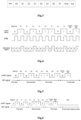
- FIG. 7 it is illustrated that a SPI signal is acquired through translation from a UART signal, and finally a differential simulation HB signal is generated by the HBS communication chip 12.
- the translation-based signal generation device 10 includes a control chip 11 and an HBS communicator 12.
- the control chip 11 is configured to generate a synchronous simulation signal based on translation from a communication signal.
- the synchronous simulation signal is in compliance with a home bus system HBS protocol.
- the HBS communicator 12 is configured to convert the synchronous simulation signal into differential simulation signals.
- the control chip 11 may be, for example, a Microchip chip or a chip or a circuit that implements a similar function
- the HBS communicator 12 may be, for example, an HBS communication chip or a chip or a circuit that implements a similar function.
- the HBS communication chip may be, for example, an MM1192 communication chip.
- the control chip 11 includes a processor 1101 and a memory 1102.
- the processor 1101 is configured to generate the synchronous simulation signal based on translation from the communication signal by looking up a preset modulation translation table.
- the memory 1102 is configured to store the modulation translation table and data of a communication signal of intention transmission.
- the modulation translation table includes a correspondence between the synchronous simulation signal in compliance with the home bus system HBS protocol and the communication signal.
- the processor 1101 includes an acquirement module 1101a and a simulation module 1101b.
- the acquirement module 1101a is configured to read each of values of bit groups for a message frame for the communication signal by a preset grouping scheme.
- the each of the values of the bit groups for the message frame includes values of one or more bits for the message frame.
- a frame for a UART signal that is not modulated by a synchronization clock includes 11 bits, and a preset grouping scheme may be offered as follows: A start bit is a first bit group, a bit 0 to a bit 3 in data bits are a second bit group, a bit 4 to a bit 7 in the data bits are a third bit group, and a parity bit and a stop bit are a fourth bit group.
- the simulation module 1101b is configured to translate each of the read values of the bit groups into a byte for the synchronous simulation signal by looking up the modulation translation table.
- the modulation translation table includes a plurality of translation subtables, each of which includes mappings from all possible values of a bit group to a corresponding byte for the synchronous simulation signal. For a value of one of the bit groups, corresponding data for the synchronous simulation signal may be acquired based on translation by looking up a corresponding translation subtable, and is usually a byte for the synchronous simulation signal.
- the control chip 11 includes a serial peripheral interface (Serial Peripheral Interface, SPI), and the serial peripheral interface has an output pin TX configured to output the synchronous simulation signal acquired upon data translation; and the HBS communicator 12 is an HBS communication chip, the HBS communication chip 12 includes an input pin IN, and the input pin IN is configured to receive the synchronous simulation signal.
- the HBS communication chip 12 generates the differential simulation signals for HBS communication based on the synchronous simulation signal.
- a level converter 13 needs to be provided for level inversion, to meet a requirement of the input pin IN of the HBS communication chip.
- the output pin TX of the serial peripheral interface is coupled to the input pin IN of the HBS communication chip through the level converter 13.
- the level converter 13 is configured to perform level inversion on the synchronous simulation signal that is output from the output pin TX of the serial peripheral interface, to meet the requirement of the input pin IN of the HBS communication chip.
- an idle level of the control chip 11 is the same as an idle level of the HBS communication chip 12, for example, both are a low level or a high level.
- the level converter 13 may not be provided between the control chip 11 and the communication chip 12.
- the control chip 11 is, for example, a Microchip chip
- the HBS communicator 12 is an HBS communication chip
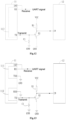
- the level converter 13 includes a triode Q1, a resistor R1, and a capacitor C1.
- the Microchip chip 11 includes a universal asynchronous receiver/transmitter (Universal Asynchronous Receiver/Transmitter, DART) input pin RX, a serial peripheral interface (Serial Peripheral Interface, SPI) output pin TX, and an interrupt pin INT.
- the HBS communication chip 12 includes an input pin IN.
- the UART input pin RX and the interrupt pin INT of the Microchip chip 11 are connected, and the UART input pin RX is configured to receive a signal.
- the SPI output pin TX is configured to output a signal, that is, from a communication signal of intention transmission, a SPI signal is generated for output based on translation in the Microchip chip 11.
- the SPI signal is in a signal format in compliance with the home bus system HBS protocol.
- the SPI signal is input to the HBS communication chip 12 through the level converter 13.
- the HBS communication chip 12 finally outputs the differential simulation signals by collecting a signal on a bus on which the input pin IN is located.
- the SPI output pin TX of the Microchip chip 11 is coupled to a base B of the triode Q1 and a first end of the capacitor C1.
- a collector C of the triode Q1 is coupled to a first end of the resistor R1 and the input pin IN of the HBS communication chip 12.
- An emitter E of the triode Q1 is grounded, a second end of the resistor R1 is coupled to a positive voltage power supply signal VCC (for example, 5 V), and a second end of the capacitor C1 is grounded.
- VCC positive voltage power supply signal
- the Microchip chip 11 may be a PIC32MX chip
- the HBS communication chip 12 may be an MM1192 communication chip. Because a SPI output pin TX of a PIC32MX series chip is at a low level in an idle state, while an idle signal as input for an input pin IN of the MM1 192 needs to be at a high level, the triode Q1 is configured to perform level inversion on the SPI signal prior to input to the MM1192.
- R1 functions as a pull-up resistor of the triode Q1, and C1 is a filter capacitor.
- the control chip 11 communicates through synchronous transmission and asynchronous reception.
- An input pin RX of a first logical communication port 113 of the control chip 11 is configured to be a UART signal receiving port, and an output pin TX of the first logical communication port 113 of the control chip is configured to be a SPI signal transmitting port.
- a serial clock (Serial Clock, SCK) port matching a SPI bus may be enabled automatically, and in this case, the SCK port cannot be used for other input/output (I/O).
- an input pin RX of a second logical communication port 111 of the control chip 11 is configured to be a UART signal receiving port
- an output pin TX0 of the second logical communication port 111 is configured to be grounded
- an output pin TX of a third logical communication port 112 is configured to be a SPI signal transmitting port
- an input pin RX0 of the third logical communication port 112 is configured to be grounded.
- a receive port of a UART of the control chip may be used to receive a signal, the receive port is configured to independently receive the signal, and a transmit port of the UART may still be used to implement another function;
- a transmit port of the SPI of the control chip may be used to transmit a signal, the transmit port is configured to independently transmit the signal, and a receive port of the SPI may still be used to implement another function.
- An embodiment of the invention further provides a home bus system (HBS) circuit, applicable to home bus (HB) communication implemented using a Microchip chip.
- HBS home bus system
- the circuit includes: the Microchip chip 11, an HBS communication chip 12, a resistor R, a capacitor C1, and a triode Q1.
- the Microchip chip 11 may receive a UART signal by using a UART input pin.
- the Microchip chip 11 is configured to generate a SPI signal based on translation from a UART signal. Every four bytes in the SPI signal are corresponding to a frame for the UART signal, a Baud rate of the SPI signal is twice a Baud rate of the UART signal, and the SPI signal is in compliance with a Home Bus System (HBS) protocol.
- the Microchip chip 1 1 transmits the SPI signal through the SPI output pin.
- the HBS communication chip 12 is configured to receive the SPI signal and output differential simulation signals.
- the Microchip chip 11 is configured to generate the SPI signal based on translation from the UART signal in a manner of: correspondingly translating a bit value "0" of a bit for the UART signal into bit values "0,1” of two bits for the SPI signal; and correspondingly translating a bit value "1” of a bit for the UART signal into bit values "1,1” of two bits for the SPI signal.
- "in compliance with the HBS protocol” means that there is a transition from “0” to “1” or vice verse, and the HBS communication chip may trigger a pulse of a differential signal based on the transition between "0" and "1".
- the Microchip chip does not have a synchronization clock I/O port or a circuit for simulating an external synchronization clock.
- the Microchip chip 11 performs data translation without referring to a synchronization clock signal.
- An embodiment of the invention further provides a translation-based signal generation method, applicable to the circuit shown in FIG. 11 .
- the method includes steps:
- the Microchip chip In the translation-based signal generation method provided in this embodiment of this application, the Microchip chip generates the SPI signal based on translation from the input UART signal by bytes, so that the SPI signal is in compliance with the home bus system HBS protocol.
- the SPI signal is used as the input to the HBS communication chip, and finally, the HBS communication chip outputs the differential simulation HB signals, to implement home bus (Home Bus) communication.
- An embodiment of this application provides a translation-based signal generation device, applicable to the foregoing method, and configured to implement home bus HB communication through a Microchip chip.
- the device includes:
- Some embodiments of the invention further provide a Home Bus System (HBS) circuit, including any translation-based signal generation device described above.
- HBS Home Bus System
- a control chip without synchronization clock signal output for example, a Microchip chip may be used.
- Some embodiments of the invention further provide a user equipment, including a home bus system HBS circuit or any translation-based signal generation device described above.
- the user equipment may be a smart household product such as an air conditioner, a refrigerator, a washing machine, a television, a kitchen appliance, or the like.
- the user equipment may be a multi-split air conditioner product.
- the user equipment may alternatively be an electronic device such as a mobile phone or a gaming device or any device that may access an HBS communication network or a similar communication network.
- the similar communication network herein refers to a communication network in which communication requires a synchronization clock signal.
- An embodiment of the invention provides a controller.
- the controller includes: a memory, configured to store a computer program and data of a communication signal of intention transmission; and a processor, configured to execute the computer program to implement the method including steps:
- An embodiment of the invention provides a computer storage medium.
- the computer storage medium is configured to store a computer program, and the computer program is executed to implement the following method:
- An embodiment of the invention provides a computer program product.
- the computer program product includes an instruction, and the instruction is run on a computer to implement the following method including steps:
- the device in this embodiment of the invention may be applicable to the foregoing method. Therefore, for technical effects the device can achieve, refer to the foregoing method embodiment, and details are not described herein again in this embodiment of the invention.
- the acquirement module and the simulation module may be separately disposed, or may be integrated into a processor of the controller, or may be implemented by program which is stored in the memory of the controller and is invoked by a processor of the controller to perform functions of the modules.
- the processor herein may be a central processing unit (Central Processing Unit, CPU) or an application-specific integrated circuit (Application-Specific Integrated Circuit, ASIC), or may be configured as one or more integrated circuits for implementing the embodiments of the invention.
- CPU Central Processing Unit
- ASIC Application-Specific Integrated Circuit
- sequence numbers of the steps do not mean particular execution sequences.
- the execution sequences of the steps should be determined based on functions and internal logic of the steps, and should not be construed as any limitation on the implementation processes of the embodiments of the invention.
- the disclosed system, device, equipment, and method may be implemented in other manners.
- the described device embodiment is merely an example.
- the function module division is merely logical function division and may be implemented by other division in actual implementation.
- a plurality of modules or components may be combined or integrated into another system, or some features may be ignored or not performed.
- the displayed or discussed mutual couplings or direct couplings or communication connections may be implemented through some interfaces.
- the indirect couplings or communication connections between the devices or function modules may be implemented in electronic, mechanical, or other forms.
- the function modules, units, or components described as separate parts may or may not be physically separate, and parts displayed as components may or may not be physical units, may be located in one position, or may be distributed on a plurality of network units. Some or all of the units may be selected based on actual needs to achieve the objectives of the solutions of the embodiments.
- function modules or elements in the embodiments of the invention may be integrated into one unit, or each of the units may exist alone physically, or two or more units are integrated into one unit.
- the steps of the method or algorithm described in the embodiments of the invention may be implemented by a processor by executing a software instruction.
- the software instruction may include a corresponding software module.
- the software module may be stored in a random access memory (Random Access Memory, RAM), a flash memory, a read-only memory (Read-Only Memory, ROM), an erasable programmable read-only memory (Erasable Programmable ROM, EPROM), an electrically erasable programmable read-only memory (Electrically EPROM, EEPROM), a register, a hard disk, a removable hard disk, a compact disc read-only memory (CD-ROM), or a storage medium in any other form well known in the art.
- RAM Random Access Memory
- ROM read-only memory
- EPROM erasable programmable read-only memory
- Electrically erasable programmable read-only memory Electrically erasable programmable read-only memory
- EEPROM electrically erasable programmable read-
- An example storage medium is coupled to the processor, so that the processor can read information from the storage medium, and can write information into the storage medium.
- the processor may be a device having a logical operation capability and/or a program execution capability, such as a central processing unit (CPU), a field programmable logic array (FPGA), a micro control unit (MCU), or an application-specific integrated circuit (ASIC).
- CPU central processing unit
- FPGA field programmable logic array
- MCU micro control unit
- ASIC application-specific integrated circuit
- the embodiments When implemented by a software program, the embodiments may be all or some implemented in a form of a computer program product.
- the computer program product includes one or more computer instructions. When the computer program instructions are loaded and executed on a computer, all or some of the procedure or functions according to the embodiments of this application are generated.
- the computer may be a general-purpose computer, a dedicated computer, a computer network, or another programming device.
- the computer instructions may be stored in a computer-readable storage medium or may be transmitted from a computer-readable storage medium to another computer-readable storage medium.
- the computer instructions may be transmitted from one website, computer, server, or data center to another website, computer, server, or data center in a wired (such as a coaxial cable, an optical fiber, or a digital subscriber line (Digital Subscriber Line, DSL)) or wireless (such as infrared, radio, or microwave) manner.
- the computer-readable storage medium may be any usable medium accessible by a computer, or a data storage device, such as a server or a data center, integrating one or more usable media.
- the usable medium may be a magnetic medium, a semiconductor medium, or the like.
- the network may include a wireless network, a wired network, and/or any combination thereof.
- the network may include a local area network, the Internet, a telecommunications network, an Internet of things based on the Internet and/or the telecommunications network, and/or any combination thereof.
- the wired network such as a twisted pair, a coaxial cable, an optical fiber, or other transmission means may be used for communication.
- the wireless network such as a 3G/4G/5G mobile communications network, Bluetooth, Zigbee, WiFi, or other transmission means may be used.
Landscapes
- Engineering & Computer Science (AREA)
- Theoretical Computer Science (AREA)
- General Engineering & Computer Science (AREA)
- Physics & Mathematics (AREA)
- General Physics & Mathematics (AREA)
- Computer Networks & Wireless Communication (AREA)
- Signal Processing (AREA)
- Computer Hardware Design (AREA)
- Information Transfer Systems (AREA)
- Dc Digital Transmission (AREA)
Description
- This application claims priority to
Chinese Patent Application No. 201710942121A filed with the China National Intellectual Property Administration on October 11, 2017 CN107770021A on 06 March 2018 , and entitled "HOME BUS SYSTEM (HBS) CIRCUIT AND TRANSLATION-BASED SIGNAL GENERATION METHOD AND DEVICE". - The present invention relates to a home bus system (HBS) circuit, a user equipment comprising a home bus system (HBS) circuit and a signal generation method implementing home bus (HB) communication.
- Multi-split products usually use a home bus (Home Bus, HB) for communication. Such a communication manner is stable and reliable, and polarity does not need to be considered for wiring.
- Due to a lack of a synchronization clock required for HomeBus communication, other types of chips do not support HomeBus communication.
-
US 2013/064321A1 discloses a method for the unidirectional, asynchronous serial data transfer with an asynchronous data format with F frame bits between a transmitting interface of a data transmitting device and between a data receiving device with a serial receiving interface comprising an asynchronous serial data input. -
US 2008/0147926A1 discloses an interface conversion device for achieving the conversion between a universal asynchronous receiver transmitter (UART) and a serial peripheral interface (SPI) by using a complex programmable logic device. - Document "Application Note On SPI Communication using UART" (12 November 2010 (2010-11-12), pages 1-7, XP055021449, Retrieved from the InternetURL:http://www.fujitsu.com/downloads/MICRO/fma/pdfmcu/SPICommunicationUsing UART.pdf) discloses how to perform SPI communication using UART.
- The invention provides a home bus system (HBS) circuit according to
independent claim 1, a user equipment according to independent claim 7 and a signal generation method according toindependent claim 13. The dependent claims relate to advantageous embodiments. - To describe the technical solutions in the embodiments of the invention to be more clear, the accompanying drawings required for describing the embodiments or the prior art are described briefly below. Apparently, the accompanying drawings according to the following description illustrate merely some of embodiments in accordance with this disclosure, and persons of ordinary skill in the art may still derive other drawings from these accompanying drawings without creative efforts.
-
FIG. 1 is a schematic flowchart of a translation-based signal generation method in accordance with an embodiment of the invention. -
FIG. 2 is a schematic flowchart of a method for generating a synchronous simulation signal according to a communication signal in accordance with an embodiment of the invention. -
FIG. 3 is a schematic diagram illustrating a frame for a UART signal. -
FIG. 4 is a schematic diagram illustrating a UART signal being modulated by using a PWM clock signal in accordance with related technologies. -
FIG. 5 is a schematic diagram illustrating a grouping scheme used for data translation in accordance with some embodiments of the invention. -
FIG. 6 is a schematic diagram illustrating another grouping scheme used for data translation in accordance with some embodiments of the invention. -
FIG. 7 is a schematic diagram illustrating a waveform correspondence between a UART signal, a SPI signal, and an HB signal in accordance with some embodiments of the invention. -
FIG. 8 is a schematic structural diagram illustrating a translation-based signal generation device in accordance with some embodiments of the invention. -
FIG. 9 is a schematic structural diagram illustrating a control chip in accordance with some embodiments of the invention. -
FIG. 10 is a schematic structural diagram illustrating a processor in accordance with some embodiments of the invention. -
FIG. 11 is a schematic structural diagram illustrating an HBS circuit in accordance with some embodiments of the invention. -
FIG. 12 is a schematic structural diagram illustrating another HBS circuit in accordance with some embodiments of the invention. -
FIG. 13 is a schematic structural diagram illustrating still another HBS circuit in accordance with some embodiments of the invention. -
FIG. 14 is a schematic flowchart of another translation-based signal generation method in accordance with an embodiment of the invention. -
FIG. 15 is a schematic structural diagram illustrating another translation-based signal generation device in accordance with some embodiments of the invention. - This disclosure provides a translation-based signal generation method and device, a home bus system (HBS) circuit, and a user equipment, to implement home bus HomeBus communication by using a chip without a synchronization clock signal, such as a Microchip chip.
- The embodiments of the invention are described below with reference to the accompanying drawings.
- As shown in
FIG. 1 , a translation-based signal generation method is provided in accordance with some embodiments of the invention, including steps: - 101. Acquire a communication signal of intention transmission, where the communication signal of intention transmission is not modulated by a synchronization clock.
- 102. Generate a synchronous simulation signal in compliance with a home bus system HBS protocol based on translation from the communication signal.
- 103. Convert the synchronous simulation signal into a differential simulation signal.
- The communication signal of intention transmission in
step 101 may be, such as a signal, with an intention for output and communication, for a chip without a synchronization clock signal, such as a Microchip chip. For example, the communication signal of intention transmission instep 101 may be a UART (Universal Asynchronous Receiver/Transmitter) signal in compliance with a UART communication protocol. The communication signal may be generated internally by a chip, or may be received from outside. Instep 102, a control chip generates the synchronous simulation signal based on translation from the communication signal. Instep 102, the synchronous simulation signal in compliance with the home bus system HBS protocol may be acquired through simulation by a program built in the control chip and based on computation of the built-in program. Instep 103, the synchronous simulation signal proceeds to be converted into the differential simulation signal. - In the translation-based signal generation method of the invention, HomeBus communication is implemented through software simulation. Compared with a solution of receiving an external synchronization clock signal and implementing HomeBus communication based on the received synchronization clock signal, the method saves I/O resources of the control chip, and leaves out some of external circuits. In the translation-based signal generation method of the invention, HomeBus communication can be implemented without a synchronization clock signal.
- In some embodiments of the invention, the synchronous simulation signal is generated based on translation from the communication signal by looking up a preset modulation translation table. The modulation translation table includes a correspondence between the communication signal and the synchronous simulation signal in compliance with the home bus system HBS protocol. In this embodiment, the synchronous simulation signal may be generated based on translation from the communication signal of intention transmission by looking up the modulation translation table. The synchronous simulation signal is in a signal format in compliance with the home bus system (HBS) protocol, and therefore, and thus an HBS communicator, such as an MM1192 communication chip, can identify the synchronous simulation signal. Such a method of data translation using a translation table may be used to simulate synchronous communication with asynchronous communication, with a faster response speed.
- As shown in
FIG. 2 , in some embodiments of the invention, the step of generating a synchronous simulation signal based on translation from the communication signal may include steps: - 1021. Read a value of each of bit groups for a message frame for the communication signal by a preset grouping scheme, where a value of one of the bit groups for the message frame includes values of one or more of the bits for the message frame.
- 1022, Translate the respective read values of the bit groups into bytes for the synchronous simulation signal by looking up the modulation translation table, where the modulation translation table includes a plurality of translation subtables, each of which includes mappings from all possible values of a bit group to a corresponding byte of a synchronous simulation signal.
- Hereinafter, for example, the communication signal is a UART signal in compliance with a UART communication protocol, and the synchronous simulation signal is a SPI signal in compliance with a SPI communication protocol. Correspondingly, a modulated signal generated through modulation based on the UART signal and an input clock signal in related technologies may be a modulated UART signal. Certainly, persons skilled in the art would understand that, the communication signal and the synchronous simulation signal may alternatively be in other signal formats, and in view of the invention, persons skilled in the art may easily acquire a corresponding method for generating a synchronous simulation signal based on translation from a communication signal.
- The UART signal is a UART signal that is not modulated by a synchronization clock. A frame for the signal may transmit 11 bits in total. Referring to
FIG. 3 , the 11 bits include one start bit, eight data bits (D0 to D7) (one byte), one parity bit, and one stop bit. - Referring to
FIG. 4 , if the UART signal is modulated by a pulse width modulation (Pulse Width Modulation, PWM) clock signal with a double frequency, a frame for the modulated signal includes 22 bits. - In some embodiments, the SPI signal is generated according to the UART signal by using an algorithm without referring to a synchronization clock signal, so that a signal format of the generated SPI signal is the same as a signal format of a modulated UART signal in related technologies that is generated upon modulation of a UART signal by referring to a synchronization clock signal. In other words, the SPI signal is in compliance with the home bus system HBS protocol.
- Every four of bytes for the SPI signal may be corresponding to a frame for the UART signal, the SPI signal has a Baud rate twice the UART signal, and the SPI signal simulates the modulated UART signal.
- The SPI signal acquired upon translation is used to simulate the modulated UART signal, and the Baud rate of the SPI signal needs to be twice the Baud rate of the UART signal. For example, assuming that the Baud rate of the UART signal is 9600 bps, the Baud rate of the output SPI signal needs to be 19200 bps.
- Each of SPI data packets of the SPI signal may include 8, 16, or 32 bits. It is assumed that eight bits are taken as a SPI data packet. In order to simulate 22 bits of a frame for the modulated UART signal, at least three SPI data packets are needed. Corresponding translations between bytes for the SPI signal and bits of a frame for the UART signal may be implemented by looking up a table, which can reach a higher translation efficiency. Alternatively, the corresponding translations between bytes for the SPI signal and bits of a frame for the UART signal may be implemented using any other methods known to persons skilled in the art, such as software programming.
- In some embodiments, a SPI data packet of four bytes may be transmitted to simulate valid data of a frame for the UART signal. For example, as shown in
FIG. 5 , in a SPI data packet, the first byte for the SPI signal is corresponding to a start bit of a frame for data of the UART signal; the second byte and the third byte for the SPI signal are corresponding to bits of the data of the UART signal, for example, the second byte for the SPI signal is corresponding to a bit 0 (D0) to a bit 3 (D3) of data bits (D0 to D7) in the frame for the data of the UART signal, and the third byte for the SPI signal is corresponding to a bit 4 (D4) to a bit 7 (D7) of data bits in the frame for the data of the UART signal; and the fourth byte for the SPI signal is corresponding to a parity bit and a stop bit for the UART signal. In other words, the start bit for the UART signal is a first bit group, corresponding to the first byte for the SPI signal; thebit 0 to the bit 3 (D0 to D3) of the data bits (D0 to D7) for the UART signal is a second bit group, corresponding to the second byte for the SPI signal; the bit 4 to the bit 7 (D4 to D7) of the data bits (D0 to D7) for the UART signal are a third bit group, corresponding to the third byte for the SPI signal; and the parity bit and the stop bit in the frame for the data of the UART signal is a fourth bit group, corresponding to the fourth byte for the SPI signal. The respective values of the bit groups for a message frame for the UART signal are read by this grouping scheme, and the corresponding SPI signal is acquired by looking up the modulation translation table. - Five arrays as below are translation subtables of the modulation translation table, and used to quickly search for a SPI data packet of four bytes upon translation by the respective values of bit groups in the message frame for the UART signal. For example, assuming that the UART signal represents "0x00", with a Baud rate 9600 bps, a SPI data packet of four bytes for the SPI signal acquired upon translation includes: "0x01 "+"0x55 "+"0x55"+"0x40", with a Baud rate 19200 bps.
- The first bit group, namely, the start bit for the original data, is corresponding to the first byte of the SPI data packet. Because all data are corresponding to the same start bit, all data elements in an array table0[256] corresponding to the first byte are 0x01.
- In software programming, a translation subtable corresponding to the first bit group, namely, the array table0[256] is presented as follows:
 const unsigned char TXnum_table0[256] = {// First Byte
      0x01,0x01,0x01,0x01,0x01,0x01,0x01,0x01,0x01,0x01,//0~9
      0x01,0x01,0x01,0x01,0x01,0x01,0x01,0x01,0x01,0x01,//10~19
      0x01,0x01,0x01,0x01,0x01,0x01,0x01,0x01,0x01,0x01,//20~29
      0x01,0x01,0x01,0x01,0x01,0x01,0x01,0x01,0x01,0x01,//30~39
      0x01,0x01,0x01,0x01,0x01,0x01,0x01,0x01,0x01,0x01,//40~49
      0x01,0x01,0x01,0x01,0x01,0x01,0x01,0x01,0x01,0x01,//50~59
      0x01,0x01,0x01,0x01,0x01,0x01,0x01,0x01,0x01,0x01,//60~69
      0x01,0x01,0x01,0x01,0x01,0x01,0x01,0x01,0x01,0x01,//70~79
      0x01,0x01,0x01,0x01,0x01,0x01,0x01,0x01,0x01,0x01,//80~89
      0x01,0x01,0x01,0x01,0x01,0x01,0x01,0x01,0x01,0x01,//90~99
      0x01,0x01,0x01,0x01,0x01,0x01,0x01,0x01,0x01,0x01,//100~109
      0x01,0x01,0x01,0x01,0x01,0x01,0x01,0x01,0x01,0x01,//110~119
      0x01,0x01,0x01,0x01,0x01,0x01,0x01,0x01,0x01,0x01,//120~129
      0x01,0x01,0x01,0x01,0x01,0x01,0x01,0x01,0x01,0x01,//130~139
      0x01,0x01,0x01,0x01,0x01,0x01,0x01,0x01,0x01,0x01,//140~149
      0x01,0x01,0x01,0x01,0x01,0x01,0x01,0x01,0x01,0x01,//150~149
      0x01,0x01,0x01,0x01,0x01,0x01,0x01,0x01,0x01,0x01,//160~169
      0x01,0x01,0x01,0x01,0x01,0x01,0x01,0x01,0x01,0x01,//170~179
      0x01,0x01,0x01,0x01,0x01.0x01,0x01,0x01,0x01,0x01,//180~189
      0x01,0x01,0x01,0x01,0x01,0x01,0x01,0x01,0x01,0x01,//190~199
      0x01,0x01,0x01,0x01,0x01,0x01,0x01,0x01,0x01,0x01,//200~209
      0x01,0x01,0x01,0x01,0x01,0x01,0x01,0x01,0x01,0x01,//210~219
      0x01,0x01,0x01,0x01,0x01,0x01,0x01,0x01,0x01,0x01,//220~229
      0x01,0x01,0x01,0x01,0x01,0x01,0x01,0x01,0x01,0x01,//230~239
      0x01,0x01,0x01,0x01,0x01,0x01,0x01,0x01,0x01,0x01,//240~249
     0x01,0x01,0x01,0x01,0x01,0x01 //250~255 }.
 const unsigned char TXnum_table1[256]={//Second Byte
      0x55,0x15,0x45,0x5,0x51,0x11,0x41,0x1,0x54,0x14,//0~9
      0x44,0x4,0x50,0x10,0x40,0x0,0x55,0x15,0x45,0x5,//10~19
      0x51,0x11,0x41,0x1,0x54,0x14,0x44,0x4,0x50,0x10,//20~29
      0x40,0x0,0x55,0x15,0x45,0x5,0x51,0x11,0x41,0x1,//30~39
      0x54,0x14,0x44,0x4,0x50,0x10,0x40,0x0,0x55,0x15, //40~49
      0x45,0x5,0x51,0x11,0x41,0x1,0x54,0x14,0x44,0x4,//50~59
      0x50,0x10,0x40,0x0,0x55,0x15,0x45,0x5,0x51,0x11,//60~69
     0x41,0x1,0x54,0x14,0x44,0x4,0x50,0x10,0x40,0x0,//70~79
      0x55,0x15,0x45,0x5,0x51,0x11,0x41,0x1,0x54,0x14,//180~89
      0x44,0x4,0x50,0x10,0x40,0x0,0x55,0x15,0x45,0x5, //90-99
      0x51,0x11,0x41,0x1,0x54,0x14,0x44,0x4,0x50,0x10, //100-109
      0x40,0x0,0x55,0x15,0x45,0x5,0x51,0x11,0x41,0x1,//110~119
      0x54,0x14,0x44,0x4,0x50,0x10,0x40,0x0,0x55,0x15, 1/120-129
      0x45,0x5,0x51,0x11,0x41,0x1,0x54,0x14,0x44,0x4,//130~139
      0x50,0x10,0x40,0x0,0x55,0x15,0x45,0x5,0x51,0x11,//140~149
      0x41,0x1,0x54,0x14,0x44,0x4,0x50,0x10,0x40,0x0,//150~159
      0x55,0x15,0x45,0x5,0x51,0x11,0x41,0x1,0x54,0x14,//160~169
      0x44,0x4,0x50,0x10,0x40,0x0,0x55,0x15,0x45,0x5,//170~179
      0x51,0x11,0x41,0x1,0x54,0x14,0x44,0x4,0x50,0x10,//180~189
      0x40,0x0,0x55,0x15,0x45,0x5,0x51,0x11,0x41,0x1,//190~199
      0x54,0x14,0x44,0x4,0x50,0x10,0x40,0x0,0x55,0x15,//200~209
      0x45,0x5,0x51,0x11,0x41,0x1,0x54,0x14,0x44,0x4,//210~219
      0x50,0x10,0x40,0x0,0x55,0x15,0x45,0x5,0x51,0x11,//220~229
      0x41,0x1,0x54,0x14,0x44,0x4,0x50,0x10,0x40,0x0,//230~239
      0x55,0x15,0x45,0x5,0x51,0x11,0x41,0x1,0x54,0x14,//240~249
      0x44,0x4,0x50,0x10,0x40,0x00 //250~255 }.
 const unsigned char TXnum_table2[256]={ //Third Byte
      0x55,0x55,0x55,0x55,0x55,0x55,0x55,0x55,0x55,0x55,//0~9
      0x55,0x55,0x55,0x55,0x55,0x55,0x15,0x15,0x15,0x15,//10~19
      0x15,0x15,0x15,0x15,0x15,0x15,0x15,0x15,0x15,0x15,//20~29
      0x15,0x15,0x45,0x45,0x45,0x45,0x45,0x45,0x45,0x45,//30~39
      0x45,0x45,0x45,0x45,0x45,0x45,0x45,0x45,0x5,0x5, //140~49
      0x5,0x5,0x5,0x5,0x5,0x5,0x5,0x5,0x5,0x5,//50~59
      0x5,0x5,0x5,0x5,0x51,0x51,0x51,0x51,0x51,0x51,//60~69
      0x51,0x51,0x51,0x51,0x51,0x51,0x51,0x51,0x51,0x51,//70~79
      0x11,0x11,0x11,0x11,0x11,0x11,0x11,0x11,0x11,0x11,//80~89
      0x11,0x11,0x11,0x11,0x11,0x11,0x41,0x41,0x41,0x41,//90~99
      0x41,0x41,0x41,0x41,0x41,0x41,0x41,0x41,0x41,0x41,//100~109
      0x41,0x41,0x1,0x1,0x1,0x1,0x1,0x1,0x1,0x1,//110~119
      0x1,0x1,0x1,0x1,0x1,0x1,0x1,0x1,0x54,0x54,//120~129
      0x54,0x54,0x54,0x54,0x54,0x54,0x54,0x54,0x54,0x54,//130~139
      0x54,0x54,0x54,0x54,0x14,0x14,0x14,0x14,0x14,0x14//140~149
      0x14,0x14,0x14,0x14,0x14,0x14,0x14,0x14,0x14,0x14,//150~159
     0x44,0x44,0x44,0x44,0x44,0x44,0x44,0x44,0x44,0x44,//160~169
     0x44,0x44,0x44,0x44,0x44,0x44,0x4,0x4,0x4,0x4,//170~179
     0x4,0x4,0x4,0x4,0x4,0x4,0x4,0x4,0x4,0x4,//180~189
     0x4,0x4,0x50,0x50,0x50,0x50,0x50,0x50,0x50,0x50,//190~199
     0x50,0x50,0x50,0x50,0x50,0x50,0x50,0x50,0x10,0x10,//200~209
     0x10,0x10,0x10,0x10,0x10,0x10,0x10,0x10,0x10,0x10,//210~219
     0x10,0x10,0x10,0x10,0x40,0x40,0x40,0x40,0x40,0x40,//220~229
     0x40,0x40,0x40,0x40,0x40,0x40,0x40,0x40,0x40,0x40,//230~239
     0x0,0x0,0x0,0x0,0x0,0x0,0x0,0x0,0x0,0x0,//240~249
      0x0,0x0,0x0,0x0,0x0,0x0 //250~255 }.
 const unsigned char TXnum_table3_1[256]={//Odd Parity Check List for Fourth Byte
      0x0,0x40,0x40,0x0,0x40,0x0,0x0,0x40,0x40,0x0,//0~9
      0x0,0x40,0x0,0x40,0x40,0x0,0x40,0x0,0x0,0x40,//10~19
      0x0,0x40,0x40,0x0,0x0,0x40,0x40,0x0,0x40,0x0,//20~29
      0x0,0x40,0x40,0x0,0x0,0x40,0x0,0x40,0x40,0x0,//30~39
      0x0,0x40,0x40,0x0,0x40,0x0,0x0,0x40,0x0,0x40,//40~49
      0x40,0x0,0x40,0x0,0x0,0x40,0x40,0x0,0x0,0x40,//50~59
      0x0,0x40,0x40,0x0,0x40,0x0,0x0,0x40,0x0,0x40,//60~69
      0x40,0x0,0x0,0x40,0x40,0x0,0x40,0x0,0x0,0x40,//70~79
      0x0,0x40,0x40,0x0,0x40,0x0,0x0,0x40,0x40,0x0,//80~89
      0x0,0x40,0x0,0x40,0x40,0x0,0x0,0x40,0x40,0x0,//90~99
      0x40,0x0,0x0,0x40,0x40,0x0,0x0,0x40,0x0,0x40,//100~109
      0x40,0x0,0x40,0x0,0x0,0x40,0x0,0x40,0x40,0x0,//110~119
      0x0,0x40,0x40,0x0,0x40,0x0,0x0,0x40,0x40,0x0,//120-129
      0x0,0x40,0x0,0x40,0x40,0x0,0x0,0x40,0x40,0x0,//130~139
      0x40,0x0,0x0,0x40,0x0,0x40,0x40,0x0,0x40,0x0,//140~149
      0x0,0x40,0x40,0x0,0x0,0x40,0x0,0x40,0x40,0x0,//150~159
      0x0,0x40,0x40,0x0,0x40,0x0,0x0,0x40,0x40,0x0,//160~169
      0x0,0x40,0x0,0x40,0x40,0x0,0x40,0x0,0x0,0x40,//170~179
      0x0,0x40,0x40,0x0,0x0,0x40,0x40,0x0,0x40,0x0,//180~189
      0x0,0x40,0x0,0x40,0x40,0x0,0x40,0x0,0x0,0x40,//190~199
      0x40,0x0,0x0,0x40,0x0,0x40,0x40,0x0,0x40,0x0,//200~209
      0x0,0x40,0x0,0x40,0x40,0x0,0x0,0x40,0x40,0x0,//210~219
      0x40,0x0,0x0,0x40,0x40,0x0,0x0,0x40,0x0,0x40,//220~229
      0x40,0x0,0x0,0x40,0x40,0x0,0x40,0x0,0x0,0x40,//230~239
      0x0,0x40,0x40,0x0,0x40,0x0,0x0,0x40,0x40,0x0,//240~249
      0x0,0x40,0x0,0x40,0x40,0x00 //250~255 }.
 const unsigned char TXnum_table3_2[256]-{//Even Parity Check List for Fourth Byte
      0x40,0x0,0x0,0x40,0x0,0x40,0x40,0x0,0x0,0x40,//0~9
      0x40,0x0,0x40,0x0,0x0,0x40,0x0,0x40,0x40,0x0,//10~19
     0x40,0x0,0x0,0x40,0x40,0x0,0x0,0x40,0x0,0x40,//20~29
      0x40,0x0,0x0,0x40,0x40,0x0,0x40,0x0,0x0,0x40,//30~39
     0x40,0x0,0x0,0x40,0x0,0x40,0x40,0x0,0x40,0x0,//40~49
      0x0,0x40,0x0,0x40,0x40,0x0,0x0,0x40,0x40,0x0,//50~59
     0x40,0x0,0x0,0x40,0x0,0x40,0x40,0x0,0x40,0x0,//60~69
     0x0,0x40,0x40,0x0,0x0,0x40,0x0,0x40,0x40,0x0,//70~79
     0x40,0x0,0x0,0x40,0x0,0x40,0x40,0x0,0x0,0x40,//80~89
     0x40,0x0,0x40,0x0,0x0,0x40,0x40,0x0,0x0,0x40,//90~99
     0x0,0x40,0x40,0x0,0x0,0x40,0x40,0x0,0x40,0x0,//100~109
     0x0,0x40,0x0,0x40,0x40,0x0,0x40,0x0,0x0,0x40,//110~119
     0x40,0x0,0x0,0x40,0x0,0x40,0x40,0x0,0x0,0x40,//120~129
      0x40,0x0,0x40,0x0,0x0,0x40,0x40,0x0,0x0,0x40,//130~139
      0x0,0x40,0x40,0x0,0x40,0x0,0x0,0x40,0x0,0x40,//140~149
      0x40,0x0,0x0,0x40,0x40,0x0,0x40,0x0,0x0,0x40,//150~159
      0x40,0x0,0x0,0x40,0x0,0x40,0x40,0x0,0x0,0x40,//160-169
      Ox40,0x0,0x40,0x0,0x0,0x40,0x0,0x40,0x40,0x0,//170~179
      0x40,0x0,0x0,0x40,0x40,0x0,0x0,0x40,0x0,0x40,//180~189
      0x40,0x0,0x40,0x0,0x0,0x40,0x0,0x40,0x40,0x0,//190~199
      0x0,0x40,0x40,0x0,0x40,0x0,0x0,0x40,0x0,0x40,//200~209
      0x40,0x0,0x40,0x0,0x0,0x40,0x40,0x0,0x0,0x40,//210~219
      0x0,0x40,0x40,0x0,0x0,0x40,0x40,0x0,0x40,0x0,//220~229
      0x0,0x40,0x40,0x0,0x0,0x40,0x0,0x40,0x40,0x0,//230~239
      0x40,0x0,0x0,0x40,0x0,0x40,0x40,0x0,0x0,0x40,//240~249
      0x40,0x0,0x40,0x0,0x0,0x40 //250~255 }.
- 201. The Microchip chip receives a UART signal through the UART input pin, where the UART signal is not modulated by a synchronization clock.
- 202. The Microchip chip generates a SPI signal based on translation from the UART signal, where every four bytes in the SPI signal are corresponding to a frame for the UART signal, a Baud rate of the SPI signal is twice a Baud rate of the UART signal, and the SPI signal is in compliance with a home bus system HBS protocol.
- 203. The Microchip chip transmits the SPI signal through the SPI output pin, where the SPI signal is used as input to the HBS communication chip so as to acquire differential simulation HB signals.
- a
receiving unit 1103, configured to receive a UART signal through a UART input pin, where the UART signal is not modulated by a synchronization clock; - a
translation unit 1104, configured to generate a SPI signal based on translation from the UART signal received by the receivingunit 1103, where every four bytes in the SPI signal are corresponding to a frame for the UART signal, a Baud rate of the SPI signal is twice a Baud rate of the UART signal, and the SPI signal is in compliance with a home bus system HBS protocol; and - a
transmitting unit 1105, configured to transmit, through a SPI output pin, the SPI signal generated by thetranslation unit 1104 through translation, where the SPI signal is used as input to an HBS communication chip to acquire a differential simulation HB signal.
- 101. Acquire a communication signal of intention transmission.
- 102. Generate a synchronous simulation signal by a control chip, where the synchronous simulation signal is in compliance with a home bus system HBS protocol.
- 103. Convert the synchronous simulation signal into a differential simulation signal.
- 101. Acquire a communication signal of intention transmission.
- 102. Generate a synchronous simulation signal by a control chip based on translation from the communication signal, where the synchronous simulation signal is in compliance with a home bus system HBS protocol.
- 103. Convert the synchronous simulation signal into a differential simulation signal.
- 101. Acquire a communication signal of intention transmission.
- 102. Generate a synchronous simulation signal by a control chip, where the synchronous simulation signal is in compliance with a home bus system HBS protocol.
- 103. Convert the synchronous simulation signal into a differential simulation signal.
Claims (14)
- A home bus system, HBS, circuit, characterized by being applicable to home bus, HB, communication implemented through a control chip (11) without a synchronization clock I/O port, wherein the circuit comprises:the control chip (11) having a serial peripheral interface (SPI) output pin (TX), andan HBS communication chip (12) having an input pin (IN),(12),wherein the SPI output pin (TX) is coupled to the input pin (IN) of the HBS communication chipwherein the control chip (11) is configured to transmit a SPI signal, for simulating a a universal asynchronous receiver/transmitter, UART, signal modulated by a synchronization clock signal, through the SPI output pin (TX).
- The HBS circuit according to claim 1, wherein the control chip (11) has UART input pin (RX).
- The HBS circuit according to claim 1, wherein every four bytes in the SPI signal are corresponding to a frame for the UART signal, the SPI signal having a Baud rate twice the UART signal.
- The HBS circuit according to claim 1, wherein a frame for the UART signal comprises a start bit, data bits, a check bit, and a stop bit, and the data bits comprise eight bits D0, D1, D2, D3, D4, D5, D6, and D7; and
wherein the modulated UART signal is simulated by the SPI signal so that the start bit is corresponding to last two bits in a first byte for the SPI signal, the data bits D0, D1, D2, and D3 are corresponding to a second byte for the SPI signal, the data bits D4, D5, D6, and D7 are corresponding to a third byte for the SPI signal, and the check bit and the stop bit are corresponding to first four bits in a fourth byte for the SPI signal. - The HBS circuit according to claim 1, wherein the modulated UART signal is simulated by the SPI signal so as to assign 0 to first six bits in the first byte for the SPI signal, and assign 0 to last four bits in the fourth byte for the SPI signal.
- The HBS circuit according to claim 1, further comprising a level converter (13) comprising a triode (Q1), a resistor (R1), and a capacitor (C1),
wherein the triode (Q1) has a base coupled to the SPI output pin (TX) and a first end of the capacitor (C1), a collector (C) coupled to a first end of the resistor (R1) and the input pin (IN) of the HBS communication chip (12), and an emitter (E) grounded, wherein a second end of the resistor (R1) is coupled to a power supply, and a second end of the capacitor (C1) is grounded. - A user equipment, comprising a home bus system, HBS, circuit, as defined in claim 1, the user equipment being characterized by being applicable to home bus, HB, communication implemented through a control chip (11) without a synchronization clock I/O port, wherein the circuit comprises:the control chip (11), configured to generate and transmit a synchronous simulation signal in compliance with a home bus system, HBS,protocol, synchronous simulation signal being for simulating a communication signal, modulated by a synchronization clock signal, of intention transmission; andan HBS communicator (12), configured to receive and convert the synchronous simulation signal from the control chip (11) into a differential simulation signal for HBS communication.
- The user equipment according to claim 7, wherein the control chip (11) comprises:a processor (1101), configured to generate the synchronous simulation signal according to the communication signal by looking up a preset modulation translation table; anda memory (1102), configured to store the modulation translation table, wherein the modulation translation table includes a correspondence between the communication signal and the synchronous simulation signal.
- The user equipment according to claim 8, wherein the processor (1101) comprises:an acquirement module (1101a), configured to read each of values of the bit groups for a message frame for the communication signal by a preset grouping scheme, wherein the each of the values of the bit groups for the message frame comprises values of one or more bits for the message frame; anda simulation module (1 101b), configured to translate each of the read values of the bit groups into a byte for the synchronous simulation signal by looking up the modulation translation table, wherein the modulation translation table comprises a plurality of translation subtables each including mappings from all possible values of a bit group to a corresponding byte for the synchronous simulation signal.
- The user equipment according to claim 7, wherein the control chip (11) comprises a serial peripheral interface, and configured to output the synchronous simulation signal through an output pin (TX) of the serial peripheral interface; and
the HBS communicator (12) comprises an input pin (IN), and configured to receive the synchronous simulation signal through the input pin (IN). - The user equipment according to claim 10, further comprising a level converter (13), whereinthe output pin (TX) of the serial peripheral interface is coupled to the input pin (IN) of the HBS communicator (12) through the level converter (13); andthe level converter (13) is configured to perform level inversion on the synchronous simulation signal output from the output pin (TX) of the serial peripheral interface, to meet a requirement of the input pin (IN) of the HBS communicator (12).
- The user equipment according to claim 11, wherein the control chip (11) is suitable for communicating through synchronous transmission and asynchronous reception; andthe control chip (11) has a first logical communication port (113) configured to have an input pin (RX) as a UART signal receiving port, and have an output pin (TX) as a SPI signal transmitting port; orthe control chip (11) has a second logical communication port (111) configured to have an input pin (RX) as a UART signal receiving port, and have an output pin (TX0) grounded, and has a third logical communication port (112) configured to have an output pin (TX) as a SPI signal transmitting port, and have an input pin (RX0) grounded.
- A signal generation method implemented by the home bus system, HBS, as defined in claim 1, said method being characterized by implementing home bus, HB, communication through a chip without a synchronization clock I/O port, said signal generation method comprising the steps of :acquiring a communication signal of intention transmission;generating and transmitting a synchronous simulation signal in compliance with a home bus system, HBS, protocol, the synchronous simulation signal being for simulating the communication signal modulated by a synchronization clock signal; andconverting the synchronous simulation signal into a differential simulation signal.
- The method according to claim 13, wherein the synchronous simulation signal is generated regardless of a synchronization clock signal.
Applications Claiming Priority (2)
| Application Number | Priority Date | Filing Date | Title |
|---|---|---|---|
| CN201710942121.1A CN107770021B (en) | 2017-10-11 | 2017-10-11 | Home bus system HBS circuit, signal conversion method and device |
| PCT/CN2018/109919 WO2019072218A1 (en) | 2017-10-11 | 2018-10-11 | Method and device for signal conversion, home bus system (hbs) circuit, and user equipment |
Publications (3)
| Publication Number | Publication Date |
|---|---|
| EP3697028A1 EP3697028A1 (en) | 2020-08-19 |
| EP3697028A4 EP3697028A4 (en) | 2020-12-16 |
| EP3697028B1 true EP3697028B1 (en) | 2023-06-21 |
Family
ID=61268046
Family Applications (1)
| Application Number | Title | Priority Date | Filing Date |
|---|---|---|---|
| EP18865821.5A Active EP3697028B1 (en) | 2017-10-11 | 2018-10-11 | Method and device for signal conversion, home bus system (hbs) circuit, and user equipment |
Country Status (4)
| Country | Link |
|---|---|
| US (1) | US11226917B2 (en) |
| EP (1) | EP3697028B1 (en) |
| CN (1) | CN107770021B (en) |
| WO (1) | WO2019072218A1 (en) |
Families Citing this family (8)
| Publication number | Priority date | Publication date | Assignee | Title |
|---|---|---|---|---|
| CN107770021B (en) * | 2017-10-11 | 2019-10-29 | 青岛海信日立空调系统有限公司 | Home bus system HBS circuit, signal conversion method and device |
| CN112003817B (en) * | 2020-06-30 | 2021-10-15 | 上海美仁半导体有限公司 | Signal conversion method, chip and household appliance |
| CN112769665B (en) * | 2021-01-14 | 2022-02-08 | 青岛海信日立空调系统有限公司 | Air conditioner communication device and communication system |
| CN113305867B (en) * | 2021-05-20 | 2023-03-14 | 上海纳深机器人有限公司 | Robot control circuit and control system supporting various AI (Artificial Intelligence) programming |
| CN113587382B (en) * | 2021-07-07 | 2022-12-20 | 青岛海信日立空调系统有限公司 | Air conditioner control method and device |
| CN116166596A (en) * | 2021-11-25 | 2023-05-26 | 青岛中弘数字技术有限公司 | HOMEBUS bus signal serial receiving method and device |
| CN114895612B (en) * | 2022-07-11 | 2022-09-27 | 深圳市杰美康机电有限公司 | Simulation system for DSP chip |
| CN117009163B (en) * | 2023-10-07 | 2024-02-27 | 西安中飞航空测试技术发展有限公司 | ARINC717 bus simulation signal source, signal simulation and acquisition board debugging method and device |
Family Cites Families (11)
| Publication number | Priority date | Publication date | Assignee | Title |
|---|---|---|---|---|
| JPS61219243A (en) * | 1985-03-26 | 1986-09-29 | Matsushita Electric Ind Co Ltd | home bath system |
| US5287547A (en) * | 1989-05-11 | 1994-02-15 | Pioneer Electronic Corporation | Transmission and reception system |
| US5237305A (en) * | 1990-11-30 | 1993-08-17 | Mitsubishi Denki Kabushiki Kaisha | Home bus system |
| JP4099352B2 (en) | 2002-06-20 | 2008-06-11 | 東芝キヤリア株式会社 | Air conditioner and interface |
| US20080147926A1 (en) * | 2006-10-18 | 2008-06-19 | Mitac International Corp. | Interface conversion device |
| CN201867801U (en) * | 2010-11-09 | 2011-06-15 | 海信(山东)空调有限公司 | Communication signal conversion device for air conditioner |
| CN102447600B (en) * | 2011-05-27 | 2014-04-16 | 青岛海信日立空调系统有限公司 | Method for realizing HOMEBUS communication by using singlechip without clock synchronization signal |
| EP2570931A1 (en) | 2011-09-14 | 2013-03-20 | VEGA Grieshaber KG | Method for asynchronous-serial data transfer over a synchronous-serial interface |
| CN202433895U (en) * | 2011-11-24 | 2012-09-12 | 三通(常州)电子科技有限公司 | Hardware gate circuit for conversion from universal asynchronous receiver/transmitter (UART) asynchronous serial bus to home bus system (HBS) bus |
| CN106569416B (en) * | 2016-10-28 | 2019-12-24 | 珠海格力电器股份有限公司 | Method and device for multiplexing serial interface and simulation debugging interface of microcontroller |
| CN107770021B (en) | 2017-10-11 | 2019-10-29 | 青岛海信日立空调系统有限公司 | Home bus system HBS circuit, signal conversion method and device |
-
2017
- 2017-10-11 CN CN201710942121.1A patent/CN107770021B/en active Active
-
2018
- 2018-10-11 EP EP18865821.5A patent/EP3697028B1/en active Active
- 2018-10-11 WO PCT/CN2018/109919 patent/WO2019072218A1/en not_active Ceased
- 2018-10-11 US US16/755,493 patent/US11226917B2/en active Active
Also Published As
| Publication number | Publication date |
|---|---|
| US11226917B2 (en) | 2022-01-18 |
| WO2019072218A1 (en) | 2019-04-18 |
| EP3697028A4 (en) | 2020-12-16 |
| US20210191891A1 (en) | 2021-06-24 |
| CN107770021B (en) | 2019-10-29 |
| EP3697028A1 (en) | 2020-08-19 |
| CN107770021A (en) | 2018-03-06 |
Similar Documents
| Publication | Publication Date | Title |
|---|---|---|
| US11226917B2 (en) | Translation-based signal generation method and device, home bus system (HBS) circuit, and user equipment | |
| US6507214B1 (en) | Digital configurable macro architecture | |
| US9772970B2 (en) | Multi-protocol serial communication interface | |
| JP2018533120A (en) | Bridging and virtualization of input / output signals in multi-node networks | |
| CN102347904B (en) | Router equipment, main card thereof and method for adapting main card to interface card | |
| CN106469127B (en) | A data access device and method | |
| CN103957198A (en) | Sensor data receiving and converting method and system | |
| KR101559089B1 (en) | Communication protocol for sharing memory resources between components of a device | |
| CN114064545B (en) | Method and device for identifying serial port function, main control chip, household electrical appliance and medium | |
| WO2024120267A1 (en) | Multi-interface conversion device and vehicle | |
| CN106161560A (en) | The communication system of appliance system | |
| CN107196975B (en) | PLC networking serial port converter of multiprotocol conversion | |
| CN202475477U (en) | Transmit-receive automatic switching circuit for converting RS485 interface into serial port | |
| CN104660372A (en) | Multichannel data transmission method and system based on asynchronous serial port of single chip microcomputer | |
| CN112817893B (en) | Bridge chip with function of expanding external device and expanding method | |
| CN1818895A (en) | Parallel and serial comprehensive bus system and data transmitting method | |
| CN103457595A (en) | Single chip microcomputer full duplex communication device and communication method | |
| CN107168923A (en) | A kind of device and method for configuring multiple FPGA | |
| CN112579495A (en) | GPIO controller | |
| CN108494889B (en) | Communication circuit and debugging method based on I2C bus | |
| CN213122983U (en) | System on chip realized based on FPGA | |
| CN211124028U (en) | Communication equipment expansion circuit, device | |
| CN106211282A (en) | Method, device and system for connecting multiple boards to Wi-Fi | |
| CN102629239A (en) | Address memory mapping system based on peripheral component interconnect (PCI) and address memory mapping method | |
| CN223637978U (en) | A slave device and communication system based on SPI communication |
Legal Events
| Date | Code | Title | Description |
|---|---|---|---|
| STAA | Information on the status of an ep patent application or granted ep patent |
Free format text: STATUS: THE INTERNATIONAL PUBLICATION HAS BEEN MADE |
|
| PUAI | Public reference made under article 153(3) epc to a published international application that has entered the european phase |
Free format text: ORIGINAL CODE: 0009012 |
|
| STAA | Information on the status of an ep patent application or granted ep patent |
Free format text: STATUS: REQUEST FOR EXAMINATION WAS MADE |
|
| 17P | Request for examination filed |
Effective date: 20200511 |
|
| AK | Designated contracting states |
Kind code of ref document: A1 Designated state(s): AL AT BE BG CH CY CZ DE DK EE ES FI FR GB GR HR HU IE IS IT LI LT LU LV MC MK MT NL NO PL PT RO RS SE SI SK SM TR |
|
| AX | Request for extension of the european patent |
Extension state: BA ME |
|
| A4 | Supplementary search report drawn up and despatched |
Effective date: 20201113 |
|
| RIC1 | Information provided on ipc code assigned before grant |
Ipc: G06F 1/04 20060101ALI20201109BHEP Ipc: G06F 13/38 20060101ALI20201109BHEP Ipc: G06F 13/40 20060101ALI20201109BHEP Ipc: H04L 12/40 20060101AFI20201109BHEP Ipc: G06F 13/42 20060101ALI20201109BHEP |
|
| DAV | Request for validation of the european patent (deleted) | ||
| DAX | Request for extension of the european patent (deleted) | ||
| STAA | Information on the status of an ep patent application or granted ep patent |
Free format text: STATUS: EXAMINATION IS IN PROGRESS |
|
| 17Q | First examination report despatched |
Effective date: 20220429 |
|
| GRAP | Despatch of communication of intention to grant a patent |
Free format text: ORIGINAL CODE: EPIDOSNIGR1 |
|
| STAA | Information on the status of an ep patent application or granted ep patent |
Free format text: STATUS: GRANT OF PATENT IS INTENDED |
|
| INTG | Intention to grant announced |
Effective date: 20230418 |
|
| GRAS | Grant fee paid |
Free format text: ORIGINAL CODE: EPIDOSNIGR3 |
|
| GRAA | (expected) grant |
Free format text: ORIGINAL CODE: 0009210 |
|
| STAA | Information on the status of an ep patent application or granted ep patent |
Free format text: STATUS: THE PATENT HAS BEEN GRANTED |
|
| AK | Designated contracting states |
Kind code of ref document: B1 Designated state(s): AL AT BE BG CH CY CZ DE DK EE ES FI FR GB GR HR HU IE IS IT LI LT LU LV MC MK MT NL NO PL PT RO RS SE SI SK SM TR |
|
| RAP3 | Party data changed (applicant data changed or rights of an application transferred) |
Owner name: QINGDAO HISENSE HITACHI AIR-CONDITIONING SYSTEMS CO., LTD. |
|
| REG | Reference to a national code |
Ref country code: CH Ref legal event code: EP |
|
| P01 | Opt-out of the competence of the unified patent court (upc) registered |
Effective date: 20230526 |
|
| REG | Reference to a national code |
Ref country code: DE Ref legal event code: R096 Ref document number: 602018052227 Country of ref document: DE |
|
| REG | Reference to a national code |
Ref country code: AT Ref legal event code: REF Ref document number: 1581710 Country of ref document: AT Kind code of ref document: T Effective date: 20230715 |
|
| REG | Reference to a national code |
Ref country code: IE Ref legal event code: FG4D |
|
| REG | Reference to a national code |
Ref country code: LT Ref legal event code: MG9D |
|
| REG | Reference to a national code |
Ref country code: NL Ref legal event code: MP Effective date: 20230621 |
|
| PG25 | Lapsed in a contracting state [announced via postgrant information from national office to epo] |
Ref country code: SE Free format text: LAPSE BECAUSE OF FAILURE TO SUBMIT A TRANSLATION OF THE DESCRIPTION OR TO PAY THE FEE WITHIN THE PRESCRIBED TIME-LIMIT Effective date: 20230621 Ref country code: NO Free format text: LAPSE BECAUSE OF FAILURE TO SUBMIT A TRANSLATION OF THE DESCRIPTION OR TO PAY THE FEE WITHIN THE PRESCRIBED TIME-LIMIT Effective date: 20230921 |
|
| REG | Reference to a national code |
Ref country code: AT Ref legal event code: MK05 Ref document number: 1581710 Country of ref document: AT Kind code of ref document: T Effective date: 20230621 |
|
| PG25 | Lapsed in a contracting state [announced via postgrant information from national office to epo] |
Ref country code: RS Free format text: LAPSE BECAUSE OF FAILURE TO SUBMIT A TRANSLATION OF THE DESCRIPTION OR TO PAY THE FEE WITHIN THE PRESCRIBED TIME-LIMIT Effective date: 20230621 Ref country code: NL Free format text: LAPSE BECAUSE OF FAILURE TO SUBMIT A TRANSLATION OF THE DESCRIPTION OR TO PAY THE FEE WITHIN THE PRESCRIBED TIME-LIMIT Effective date: 20230621 Ref country code: LV Free format text: LAPSE BECAUSE OF FAILURE TO SUBMIT A TRANSLATION OF THE DESCRIPTION OR TO PAY THE FEE WITHIN THE PRESCRIBED TIME-LIMIT Effective date: 20230621 Ref country code: LT Free format text: LAPSE BECAUSE OF FAILURE TO SUBMIT A TRANSLATION OF THE DESCRIPTION OR TO PAY THE FEE WITHIN THE PRESCRIBED TIME-LIMIT Effective date: 20230621 Ref country code: HR Free format text: LAPSE BECAUSE OF FAILURE TO SUBMIT A TRANSLATION OF THE DESCRIPTION OR TO PAY THE FEE WITHIN THE PRESCRIBED TIME-LIMIT Effective date: 20230621 Ref country code: GR Free format text: LAPSE BECAUSE OF FAILURE TO SUBMIT A TRANSLATION OF THE DESCRIPTION OR TO PAY THE FEE WITHIN THE PRESCRIBED TIME-LIMIT Effective date: 20230922 |
|
| PG25 | Lapsed in a contracting state [announced via postgrant information from national office to epo] |
Ref country code: FI Free format text: LAPSE BECAUSE OF FAILURE TO SUBMIT A TRANSLATION OF THE DESCRIPTION OR TO PAY THE FEE WITHIN THE PRESCRIBED TIME-LIMIT Effective date: 20230621 |
|
| PG25 | Lapsed in a contracting state [announced via postgrant information from national office to epo] |
Ref country code: SK Free format text: LAPSE BECAUSE OF FAILURE TO SUBMIT A TRANSLATION OF THE DESCRIPTION OR TO PAY THE FEE WITHIN THE PRESCRIBED TIME-LIMIT Effective date: 20230621 |
|
| PG25 | Lapsed in a contracting state [announced via postgrant information from national office to epo] |
Ref country code: ES Free format text: LAPSE BECAUSE OF FAILURE TO SUBMIT A TRANSLATION OF THE DESCRIPTION OR TO PAY THE FEE WITHIN THE PRESCRIBED TIME-LIMIT Effective date: 20230621 |
|
| PG25 | Lapsed in a contracting state [announced via postgrant information from national office to epo] |
Ref country code: IS Free format text: LAPSE BECAUSE OF FAILURE TO SUBMIT A TRANSLATION OF THE DESCRIPTION OR TO PAY THE FEE WITHIN THE PRESCRIBED TIME-LIMIT Effective date: 20231021 |
|
| PG25 | Lapsed in a contracting state [announced via postgrant information from national office to epo] |
Ref country code: SM Free format text: LAPSE BECAUSE OF FAILURE TO SUBMIT A TRANSLATION OF THE DESCRIPTION OR TO PAY THE FEE WITHIN THE PRESCRIBED TIME-LIMIT Effective date: 20230621 Ref country code: SK Free format text: LAPSE BECAUSE OF FAILURE TO SUBMIT A TRANSLATION OF THE DESCRIPTION OR TO PAY THE FEE WITHIN THE PRESCRIBED TIME-LIMIT Effective date: 20230621 Ref country code: RO Free format text: LAPSE BECAUSE OF FAILURE TO SUBMIT A TRANSLATION OF THE DESCRIPTION OR TO PAY THE FEE WITHIN THE PRESCRIBED TIME-LIMIT Effective date: 20230621 Ref country code: PT Free format text: LAPSE BECAUSE OF FAILURE TO SUBMIT A TRANSLATION OF THE DESCRIPTION OR TO PAY THE FEE WITHIN THE PRESCRIBED TIME-LIMIT Effective date: 20231023 Ref country code: IS Free format text: LAPSE BECAUSE OF FAILURE TO SUBMIT A TRANSLATION OF THE DESCRIPTION OR TO PAY THE FEE WITHIN THE PRESCRIBED TIME-LIMIT Effective date: 20231021 Ref country code: ES Free format text: LAPSE BECAUSE OF FAILURE TO SUBMIT A TRANSLATION OF THE DESCRIPTION OR TO PAY THE FEE WITHIN THE PRESCRIBED TIME-LIMIT Effective date: 20230621 Ref country code: EE Free format text: LAPSE BECAUSE OF FAILURE TO SUBMIT A TRANSLATION OF THE DESCRIPTION OR TO PAY THE FEE WITHIN THE PRESCRIBED TIME-LIMIT Effective date: 20230621 Ref country code: CZ Free format text: LAPSE BECAUSE OF FAILURE TO SUBMIT A TRANSLATION OF THE DESCRIPTION OR TO PAY THE FEE WITHIN THE PRESCRIBED TIME-LIMIT Effective date: 20230621 Ref country code: AT Free format text: LAPSE BECAUSE OF FAILURE TO SUBMIT A TRANSLATION OF THE DESCRIPTION OR TO PAY THE FEE WITHIN THE PRESCRIBED TIME-LIMIT Effective date: 20230621 |
|
| PG25 | Lapsed in a contracting state [announced via postgrant information from national office to epo] |
Ref country code: PL Free format text: LAPSE BECAUSE OF FAILURE TO SUBMIT A TRANSLATION OF THE DESCRIPTION OR TO PAY THE FEE WITHIN THE PRESCRIBED TIME-LIMIT Effective date: 20230621 |
|
| REG | Reference to a national code |
Ref country code: DE Ref legal event code: R097 Ref document number: 602018052227 Country of ref document: DE |
|
| PLBE | No opposition filed within time limit |
Free format text: ORIGINAL CODE: 0009261 |
|
| STAA | Information on the status of an ep patent application or granted ep patent |
Free format text: STATUS: NO OPPOSITION FILED WITHIN TIME LIMIT |
|
| PG25 | Lapsed in a contracting state [announced via postgrant information from national office to epo] |
Ref country code: DK Free format text: LAPSE BECAUSE OF FAILURE TO SUBMIT A TRANSLATION OF THE DESCRIPTION OR TO PAY THE FEE WITHIN THE PRESCRIBED TIME-LIMIT Effective date: 20230621 |
|
| PG25 | Lapsed in a contracting state [announced via postgrant information from national office to epo] |
Ref country code: SI Free format text: LAPSE BECAUSE OF FAILURE TO SUBMIT A TRANSLATION OF THE DESCRIPTION OR TO PAY THE FEE WITHIN THE PRESCRIBED TIME-LIMIT Effective date: 20230621 |
|
| 26N | No opposition filed |
Effective date: 20240322 |
|
| PG25 | Lapsed in a contracting state [announced via postgrant information from national office to epo] |
Ref country code: MC Free format text: LAPSE BECAUSE OF FAILURE TO SUBMIT A TRANSLATION OF THE DESCRIPTION OR TO PAY THE FEE WITHIN THE PRESCRIBED TIME-LIMIT Effective date: 20230621 Ref country code: SI Free format text: LAPSE BECAUSE OF FAILURE TO SUBMIT A TRANSLATION OF THE DESCRIPTION OR TO PAY THE FEE WITHIN THE PRESCRIBED TIME-LIMIT Effective date: 20230621 Ref country code: IT Free format text: LAPSE BECAUSE OF FAILURE TO SUBMIT A TRANSLATION OF THE DESCRIPTION OR TO PAY THE FEE WITHIN THE PRESCRIBED TIME-LIMIT Effective date: 20230621 |
|
| REG | Reference to a national code |
Ref country code: CH Ref legal event code: PL |
|
| REG | Reference to a national code |
Ref country code: BE Ref legal event code: MM Effective date: 20231031 |
|
| PG25 | Lapsed in a contracting state [announced via postgrant information from national office to epo] |
Ref country code: LU Free format text: LAPSE BECAUSE OF NON-PAYMENT OF DUE FEES Effective date: 20231011 |
|
| PG25 | Lapsed in a contracting state [announced via postgrant information from national office to epo] |
Ref country code: LU Free format text: LAPSE BECAUSE OF NON-PAYMENT OF DUE FEES Effective date: 20231011 |
|
| PG25 | Lapsed in a contracting state [announced via postgrant information from national office to epo] |
Ref country code: CH Free format text: LAPSE BECAUSE OF NON-PAYMENT OF DUE FEES Effective date: 20231031 |
|
| PG25 | Lapsed in a contracting state [announced via postgrant information from national office to epo] |
Ref country code: CH Free format text: LAPSE BECAUSE OF NON-PAYMENT OF DUE FEES Effective date: 20231031 |
|
| PG25 | Lapsed in a contracting state [announced via postgrant information from national office to epo] |
Ref country code: BE Free format text: LAPSE BECAUSE OF NON-PAYMENT OF DUE FEES Effective date: 20231031 |
|
| PG25 | Lapsed in a contracting state [announced via postgrant information from national office to epo] |
Ref country code: IE Free format text: LAPSE BECAUSE OF NON-PAYMENT OF DUE FEES Effective date: 20231011 |
|
| PG25 | Lapsed in a contracting state [announced via postgrant information from national office to epo] |
Ref country code: IE Free format text: LAPSE BECAUSE OF NON-PAYMENT OF DUE FEES Effective date: 20231011 |
|
| PG25 | Lapsed in a contracting state [announced via postgrant information from national office to epo] |
Ref country code: BG Free format text: LAPSE BECAUSE OF FAILURE TO SUBMIT A TRANSLATION OF THE DESCRIPTION OR TO PAY THE FEE WITHIN THE PRESCRIBED TIME-LIMIT Effective date: 20230621 |
|
| PG25 | Lapsed in a contracting state [announced via postgrant information from national office to epo] |
Ref country code: BG Free format text: LAPSE BECAUSE OF FAILURE TO SUBMIT A TRANSLATION OF THE DESCRIPTION OR TO PAY THE FEE WITHIN THE PRESCRIBED TIME-LIMIT Effective date: 20230621 |
|
| PG25 | Lapsed in a contracting state [announced via postgrant information from national office to epo] |
Ref country code: CY Free format text: LAPSE BECAUSE OF FAILURE TO SUBMIT A TRANSLATION OF THE DESCRIPTION OR TO PAY THE FEE WITHIN THE PRESCRIBED TIME-LIMIT; INVALID AB INITIO Effective date: 20181011 |
|
| PG25 | Lapsed in a contracting state [announced via postgrant information from national office to epo] |
Ref country code: HU Free format text: LAPSE BECAUSE OF FAILURE TO SUBMIT A TRANSLATION OF THE DESCRIPTION OR TO PAY THE FEE WITHIN THE PRESCRIBED TIME-LIMIT; INVALID AB INITIO Effective date: 20181011 |
|
| PG25 | Lapsed in a contracting state [announced via postgrant information from national office to epo] |
Ref country code: TR Free format text: LAPSE BECAUSE OF FAILURE TO SUBMIT A TRANSLATION OF THE DESCRIPTION OR TO PAY THE FEE WITHIN THE PRESCRIBED TIME-LIMIT Effective date: 20230621 |
|
| PGFP | Annual fee paid to national office [announced via postgrant information from national office to epo] |
Ref country code: DE Payment date: 20251021 Year of fee payment: 8 |
|
| PGFP | Annual fee paid to national office [announced via postgrant information from national office to epo] |
Ref country code: GB Payment date: 20251022 Year of fee payment: 8 |
|
| PGFP | Annual fee paid to national office [announced via postgrant information from national office to epo] |
Ref country code: FR Payment date: 20251030 Year of fee payment: 8 |