EP3697023A1 - Fpga device and cloud system based on fpga device - Google Patents
Fpga device and cloud system based on fpga device Download PDFInfo
- Publication number
- EP3697023A1 EP3697023A1 EP18866716.6A EP18866716A EP3697023A1 EP 3697023 A1 EP3697023 A1 EP 3697023A1 EP 18866716 A EP18866716 A EP 18866716A EP 3697023 A1 EP3697023 A1 EP 3697023A1
- Authority
- EP
- European Patent Office
- Prior art keywords
- user logic
- fpga device
- user
- functional unit
- logic unit
- Prior art date
- Legal status (The legal status is an assumption and is not a legal conclusion. Google has not performed a legal analysis and makes no representation as to the accuracy of the status listed.)
- Granted
Links
Images



Classifications
-
- H—ELECTRICITY
- H04—ELECTRIC COMMUNICATION TECHNIQUE
- H04L—TRANSMISSION OF DIGITAL INFORMATION, e.g. TELEGRAPHIC COMMUNICATION
- H04L67/00—Network arrangements or protocols for supporting network services or applications
- H04L67/01—Protocols
- H04L67/02—Protocols based on web technology, e.g. hypertext transfer protocol [HTTP]
- H04L67/025—Protocols based on web technology, e.g. hypertext transfer protocol [HTTP] for remote control or remote monitoring of applications
-
- H—ELECTRICITY
- H04—ELECTRIC COMMUNICATION TECHNIQUE
- H04L—TRANSMISSION OF DIGITAL INFORMATION, e.g. TELEGRAPHIC COMMUNICATION
- H04L41/00—Arrangements for maintenance, administration or management of data switching networks, e.g. of packet switching networks
- H04L41/08—Configuration management of networks or network elements
- H04L41/0803—Configuration setting
- H04L41/0813—Configuration setting characterised by the conditions triggering a change of settings
- H04L41/082—Configuration setting characterised by the conditions triggering a change of settings the condition being updates or upgrades of network functionality
-
- G—PHYSICS
- G01—MEASURING; TESTING
- G01R—MEASURING ELECTRIC VARIABLES; MEASURING MAGNETIC VARIABLES
- G01R31/00—Arrangements for testing electric properties; Arrangements for locating electric faults; Arrangements for electrical testing characterised by what is being tested not provided for elsewhere
- G01R31/28—Testing of electronic circuits, e.g. by signal tracer
- G01R31/317—Testing of digital circuits
- G01R31/3181—Functional testing
- G01R31/3185—Reconfiguring for testing, e.g. LSSD, partitioning
- G01R31/318533—Reconfiguring for testing, e.g. LSSD, partitioning using scanning techniques, e.g. LSSD, Boundary Scan, JTAG
-
- G—PHYSICS
- G06—COMPUTING OR CALCULATING; COUNTING
- G06F—ELECTRIC DIGITAL DATA PROCESSING
- G06F1/00—Details not covered by groups G06F3/00 - G06F13/00 and G06F21/00
- G06F1/26—Power supply means, e.g. regulation thereof
- G06F1/32—Means for saving power
- G06F1/3203—Power management, i.e. event-based initiation of a power-saving mode
- G06F1/3206—Monitoring of events, devices or parameters that trigger a change in power modality
- G06F1/3215—Monitoring of peripheral devices
-
- G—PHYSICS
- G06—COMPUTING OR CALCULATING; COUNTING
- G06F—ELECTRIC DIGITAL DATA PROCESSING
- G06F11/00—Error detection; Error correction; Monitoring
- G06F11/07—Responding to the occurrence of a fault, e.g. fault tolerance
- G06F11/14—Error detection or correction of the data by redundancy in operations
- G06F11/1402—Saving, restoring, recovering or retrying
- G06F11/1415—Saving, restoring, recovering or retrying at system level
- G06F11/1441—Resetting or repowering
-
- G—PHYSICS
- G06—COMPUTING OR CALCULATING; COUNTING
- G06F—ELECTRIC DIGITAL DATA PROCESSING
- G06F13/00—Interconnection of, or transfer of information or other signals between, memories, input/output devices or central processing units
- G06F13/38—Information transfer, e.g. on bus
- G06F13/42—Bus transfer protocol, e.g. handshake; Synchronisation
- G06F13/4282—Bus transfer protocol, e.g. handshake; Synchronisation on a serial bus, e.g. I2C bus, SPI bus
-
- G—PHYSICS
- G06—COMPUTING OR CALCULATING; COUNTING
- G06F—ELECTRIC DIGITAL DATA PROCESSING
- G06F21/00—Security arrangements for protecting computers, components thereof, programs or data against unauthorised activity
- G06F21/70—Protecting specific internal or peripheral components, in which the protection of a component leads to protection of the entire computer
- G06F21/71—Protecting specific internal or peripheral components, in which the protection of a component leads to protection of the entire computer to assure secure computing or processing of information
- G06F21/76—Protecting specific internal or peripheral components, in which the protection of a component leads to protection of the entire computer to assure secure computing or processing of information in application-specific integrated circuits [ASIC] or field-programmable devices, e.g. field-programmable gate arrays [FPGA] or programmable logic devices [PLD]
-
- G—PHYSICS
- G06—COMPUTING OR CALCULATING; COUNTING
- G06F—ELECTRIC DIGITAL DATA PROCESSING
- G06F30/00—Computer-aided design [CAD]
- G06F30/30—Circuit design
- G06F30/34—Circuit design for reconfigurable circuits, e.g. field programmable gate arrays [FPGA] or programmable logic devices [PLD]
- G06F30/343—Logical level
-
- G—PHYSICS
- G06—COMPUTING OR CALCULATING; COUNTING
- G06F—ELECTRIC DIGITAL DATA PROCESSING
- G06F8/00—Arrangements for software engineering
- G06F8/60—Software deployment
- G06F8/65—Updates
-
- G—PHYSICS
- G06—COMPUTING OR CALCULATING; COUNTING
- G06F—ELECTRIC DIGITAL DATA PROCESSING
- G06F8/00—Arrangements for software engineering
- G06F8/60—Software deployment
- G06F8/65—Updates
- G06F8/654—Updates using techniques specially adapted for alterable solid state memories, e.g. for EEPROM or flash memories
-
- G—PHYSICS
- G06—COMPUTING OR CALCULATING; COUNTING
- G06F—ELECTRIC DIGITAL DATA PROCESSING
- G06F9/00—Arrangements for program control, e.g. control units
- G06F9/06—Arrangements for program control, e.g. control units using stored programs, i.e. using an internal store of processing equipment to receive or retain programs
- G06F9/30—Arrangements for executing machine instructions, e.g. instruction decode
- G06F9/30098—Register arrangements
-
- G—PHYSICS
- G06—COMPUTING OR CALCULATING; COUNTING
- G06F—ELECTRIC DIGITAL DATA PROCESSING
- G06F9/00—Arrangements for program control, e.g. control units
- G06F9/06—Arrangements for program control, e.g. control units using stored programs, i.e. using an internal store of processing equipment to receive or retain programs
- G06F9/30—Arrangements for executing machine instructions, e.g. instruction decode
- G06F9/38—Concurrent instruction execution, e.g. pipeline or look ahead
- G06F9/3861—Recovery, e.g. branch miss-prediction, exception handling
-
- H—ELECTRICITY
- H04—ELECTRIC COMMUNICATION TECHNIQUE
- H04L—TRANSMISSION OF DIGITAL INFORMATION, e.g. TELEGRAPHIC COMMUNICATION
- H04L41/00—Arrangements for maintenance, administration or management of data switching networks, e.g. of packet switching networks
- H04L41/08—Configuration management of networks or network elements
- H04L41/0803—Configuration setting
-
- H—ELECTRICITY
- H04—ELECTRIC COMMUNICATION TECHNIQUE
- H04L—TRANSMISSION OF DIGITAL INFORMATION, e.g. TELEGRAPHIC COMMUNICATION
- H04L67/00—Network arrangements or protocols for supporting network services or applications
- H04L67/2866—Architectures; Arrangements
- H04L67/30—Profiles
-
- G—PHYSICS
- G06—COMPUTING OR CALCULATING; COUNTING
- G06F—ELECTRIC DIGITAL DATA PROCESSING
- G06F2213/00—Indexing scheme relating to interconnection of, or transfer of information or other signals between, memories, input/output devices or central processing units
- G06F2213/0026—PCI express
-
- G—PHYSICS
- G06—COMPUTING OR CALCULATING; COUNTING
- G06F—ELECTRIC DIGITAL DATA PROCESSING
- G06F2221/00—Indexing scheme relating to security arrangements for protecting computers, components thereof, programs or data against unauthorised activity
- G06F2221/21—Indexing scheme relating to G06F21/00 and subgroups addressing additional information or applications relating to security arrangements for protecting computers, components thereof, programs or data against unauthorised activity
- G06F2221/2141—Access rights, e.g. capability lists, access control lists, access tables, access matrices
-
- H—ELECTRICITY
- H04—ELECTRIC COMMUNICATION TECHNIQUE
- H04L—TRANSMISSION OF DIGITAL INFORMATION, e.g. TELEGRAPHIC COMMUNICATION
- H04L41/00—Arrangements for maintenance, administration or management of data switching networks, e.g. of packet switching networks
- H04L41/28—Restricting access to network management systems or functions, e.g. using authorisation function to access network configuration
-
- Y—GENERAL TAGGING OF NEW TECHNOLOGICAL DEVELOPMENTS; GENERAL TAGGING OF CROSS-SECTIONAL TECHNOLOGIES SPANNING OVER SEVERAL SECTIONS OF THE IPC; TECHNICAL SUBJECTS COVERED BY FORMER USPC CROSS-REFERENCE ART COLLECTIONS [XRACs] AND DIGESTS
- Y02—TECHNOLOGIES OR APPLICATIONS FOR MITIGATION OR ADAPTATION AGAINST CLIMATE CHANGE
- Y02D—CLIMATE CHANGE MITIGATION TECHNOLOGIES IN INFORMATION AND COMMUNICATION TECHNOLOGIES [ICT], I.E. INFORMATION AND COMMUNICATION TECHNOLOGIES AIMING AT THE REDUCTION OF THEIR OWN ENERGY USE
- Y02D10/00—Energy efficient computing, e.g. low power processors, power management or thermal management
Definitions
- the present invention relates to the field of cloud computing, and, more particularly, to an FPGA device and a cloud system based on the FPGA device.
- JTAG Joint Test Action Group
- Embodiments of the present invention provide an FPGA device and a cloud system based on the FPGA device, for at least resolving the technical problem that an existing FPGA cannot be deployed in the cloud due to the need for connecting to a JTAG cable when being remotely configured or debugged.
- an FPGA device comprising: a management logic unit and a user logic unit, where the management logic unit comprises a Peripheral Component Interconnect Express (PCIe) module, and the PCIe module comprises a first physical functional unit and a second physical functional unit.
- the first physical functional unit is configured to receive a user logic loading request initiated by the second physical functional unit, where the user logic loading request carries a user logic identifier; obtain a user logic file based on the user logic identifier; and burn the user logic file into the user logic unit via a PCIe configuration channel.
- PCIe Peripheral Component Interconnect Express
- a cloud system based on an FPGA device comprising: a host; and an FPGA device with any of the features mentioned above.
- the PCIe module is configured in the management logic unit of the FPGA device, and the PCIe module is divided into physical functional units with different permissions, and the management logic unit and the user logic unit are administered through configuration.
- the management logic unit comprises a PCIe module, and the PCIe module comprises a first physical functional unit and a second physical functional unit.
- the first physical functional unit is configured to receive a user logic loading request initiated by the second physical functional unit, where the user logic loading request carries a user logic identifier; obtain a user logic file based on the user logic identifier; and burn the user logic file into the user logic unit via a PCIe configuration channel.
- remote configuration is achieved without connecting to a JTAG cable when in communication with the host, so as to achieve the technical effects of improving the performance of the FPGA, thereby resolving the technical problem that an existing FPGA cannot be deployed in the cloud due to the need for connecting to a JTAG cable when being remotely configured or debugged.
- an embodiment of an FPGA device is further provided. It should be noted that before further describing the details of each embodiment of the present application, a suitable FPGA device that can be used to implement the principle of this application will be described with reference to FIG. 1 .
- FIG. 1 is a schematic structural diagram of an FPGA device according to an embodiment of the present application.
- the structure drawn is only an example of a suitable environment, and does not impose any limitation to the scope of use or function of the present application. Nor should this FPGA device be interpreted as being dependent on or requiring for any of the components or combinations shown in FIG. 1 .
- FPGA As a semi-customized circuit in the field of ASIC, FPGA not only solves the shortcomings of customized circuits, but also overcomes the limitations of gate circuit book of the original programmable devices.
- FPGA can be widely used in national defense fields such as aerospace, aviation, electronics, communication, and radar. It can also be used in medical equipment, including ultrasonic detector and CT scanning instrument, as well as in fields of consumer electronics, automotive electronics, robots and data mining. Additionally, with the rise of robot, UAV, big data, Internet of Things, unmanned driving and 5G communication, the market prospect of FPGA will be increasingly broad while maintaining steady growth.
- the FPGA device in addition to implementing the basic data transmission function, can also realize auxiliary functions, such as, remote debugging, remote upgrade, exception handling and hardware monitoring. This conforms to the use environment of the FPGA in cloud, and can thus provide reliable, stable, easy-to-use and safe FPGA acceleration cloud service.
- FIG. 1 shows the schematic diagram of an FPGA device.
- an FPGA device 1 comprises: a management logic unit 10 and a user logic unit 12.
- the management logic unit 10 comprises a PCIe module 101, and the PCIe module 101 comprises a first PF (Physical Functional unit) 1010 and a second PF 1012.
- the first PF 1010 is configured to receive a user logic loading request initiated by the second PF 1012, where the user logic loading request carries a user logic identifier; obtain a user logic file based on the user logic identifier; and burn the user logic file into the user logic unit via a PCIe configuration channel.
- the FPGA device provided in this application is suitable for setting up the FPGA cloud server architecture deployed in the cloud, thus realizing the functions of remote debugging, remote upgrading, exception handling and hardware monitoring.
- the hardware logic on the FPGA device can be divided into two parts: the management logic unit and the user logic unit.
- management logic unit can be provided by the FPGA server (for example, cloud server), while the user logic unit can be provided by an end user and a third-party IP manufacturer.
- the management logic unit can be used for peripheral communication, and the user logic unit can be used to implement the hotspot module of user application programs.
- the user logic can realize the actual compression/decompression algorithm (such as the gizp algorithm).
- Data to be compressed is sent to the FPGA device from a host CPU through PCIe, and the compressed data then returns to the host CPU from a PCIe interface.
- peripheral communication can be, but is not limited to, any of the following forms of communication: communication with the host CPU through PCIe, communication with other network devices through Ethernet or optical fiber interfaces, and communication with external storage devices through DDR (Double Data Rate) controller interfaces/Flash interfaces.
- DDR Double Data Rate
- the above-mentioned user logic unit can be replaced based on requirements.
- dynamic reconfiguration can be performed by the management logic unit.
- the dynamic reconfiguration can be implemented by using the Partial Reconfiguration (PR) function in FPGA.
- PR Partial Reconfiguration
- the management logic unit on the FPGA device can communicate with the host CPU via the PCIe module, and the PCIe module can be comprised of two or more PFs with different permissions.
- the PCIe module may be comprised of, without limitation to, a first PF and a second PF (i.e., the permission segmentation mode of the dual PFs).
- the above isolation method can be either two virtual machines or a virtual machine and the host.
- the first PF can call management.ko in the management environment of the host and the second PF can call dma.ko in the management environment of the host.
- the first PF communicates with the management environment in the host CPU
- the second PF communicates with the user environment in the host CPU.
- the first PF and the second PF can also be separate physically, and there are different configuration spaces and other permission segmentation methods between them.
- the PCIe module of the FPGA device is divided into PFs with different permissions, and the host is divided into a management environment and a user environment associated with them to realize security isolation.
- Ordinary users can only use the user environment to access the user logic and conduct remote debugging for the user logic.
- Super administrator users can use the management environment to conduct operations with higher permission, such as management, monitoring, and reconfiguration, etc. to a board card.
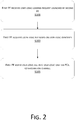
- the first PF can implement dynamic reconfiguration through, but not limited to, the following ways: Step S101, the first PF receives a user logic loading request initiated by the second PF.
- the user logic loading request carries a user logic identifier.
- the second PF can send a user logic loading request to the server based on its own identity.
- Step S103 the first PF obtains a user logic file based on the user logic identifier.
- the first PF can obtain the user logic file from a remote storage side based on the above user logic identifier after the server loads the authentication request and responds.
- Step S105 the first PF burns the user logic file into the user logic unit via a PCIe configuration channel.
- the first PF can burn the user logic file into the user logic unit via the partial reconfiguration control (PR ctrl) module in the PCIe configuration channel, and load a corresponding mirror image based on the user logic loading request.
- PR ctrl partial reconfiguration control
- the FPGA device provided in the present application can complete the dynamic reconfiguration.
- the first PF can also be configured to implement dynamic reconfiguration, remote upgrade Flash, exception handling, and hardware monitoring.
- the second PF can also be configured to conduct high-speed data exchange with the user logic unit via DMA and realize the remote debugging function of the user logic unit.
- the FPGA device provided in the present application comprises a management logic unit and a user logic unit, where the management logic unit comprises a PCIe module, and the PCIe module comprises a first physical device PF and a second PF.
- the first PF is configured to receive a user logic loading request initiated by the second PF, where the user logic loading request carries a user logic identifier; obtain a user logic file based on the user logic identifier; and burn the user logic file into the user logic unit via a PCIe configuration channel.
- the hardware logic of the FPGA device in this application can be divided into a management logic unit and a user logic unit.
- the management logic unit communicates with the host CPU via the PCIe module.
- the FPGA device in the embodiment of the present application can realize dynamic reconfiguration by security isolation via permission segmentation of two or more PFs in the PCIe module.
- the first PF can also be configured to implement dynamic reconfiguration, remote upgrade Flash, exception handling, and hardware monitoring.
- the second PF can also be configured to conduct high-speed data exchange with the user logic unit via DMA and implement the remote debugging function of the user logic unit.
- the PCIe module is configured in the management logic unit of the FPGA device, and the PCIe module is divided into PFs with different permissions to achieve remote configuration without connecting to a JTAG cable when in communication with the host. This realizes the technical effect of improving the performance of FPGA, and further solves the technical problem that an existing FPGA cannot be deployed in the cloud due to the need for connecting to a JTAG cable when being remotely configured or debugged.
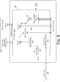
- FIG. 3 is a schematic structural diagram of an optional FPGA device according to an embodiment of the present application.
- the management logic unit further comprises a storage medium control module 103.
- the first PF is further configured to receive an upgrade request sent by a server; and obtain an upgrade file from a host via a PCIe interface based on the upgrade request.
- the storage medium control module is connected with the first PF to upgrade a storage medium based on the upgrade file.
- remote upgrade storage media is similar to that of the above-mentioned dynamic reconfiguration of the present application.
- the difference is that the upgrade request submitted by a cloud management and control system (server) is sent to an external storage side, and a command is sent to the first PF.
- server cloud management and control system
- the storage medium control module 103 is connected with a Flash (storage medium), and the first PF 1010 is connected with the storage medium control module 103.
- the first PF obtains the upgrade file from the host via the PCIe interface based on the upgrade request, and reads as well as writes the register via PCIe.
- the storage medium control (Flash ctrl) module in the management logic unit is configured to upgrade Flash firmware on a board card.
- the management logic unit also comprises an external memory controller 105, i.e. DDR Ctrl, which is connected with an external memory DDR for reading and writing the external memory DDR.
- DDR Ctrl an external memory controller 105
- the FPGA device also comprises a shared register.
- the second PF is further configured to report exception information via the shared register.
- the first PF is further configured to obtain the exception information from the shared register and perform an operation corresponding to the exception information.
- an exception handling mechanism for the FPGA device can be implemented via internal shared registers.
- FIG. 4 is a schematic structural diagram of a connection between the shared register and PF in an optional FPGA device according to an embodiment of the present application.
- the shared register is connected with the first PF and the second PF.
- the second PF can read and write the shared register as well as report the internal exception information via the shared register, and the first PF can read the shared register and poll the shared register to obtain the exception information reported by the shared register.
- the user logic unit comprises a direct access interface 107.
- the second PF is further configured to exchange data with the user logic unit via a direct access interface.
- a DMA interface can be the direct access interface.
- the DMA interface used to provide user logic belongs to the standard protocol interface, so as to guarantee the DMA interface access of the second PF exclusive PCIe.
- the user logic unit adopts the read interface in the direct access interface to move data from the host to DMA.
- the user logic unit adopts the write interface in the direct access interface to move the FPGA data to the host, thereby realizing data exchange between the host and FPGA device.
- DMA interface of FPGA logic provided to the second PF can abstract the hardware interface, thereby achieving the purpose of security isolation and simplified programming.
- the management logic unit also comprises a virtual JTAG module 109.
- the second PF is configured to obtain debugging data of the user logic unit, and the virtual JTAG module is connected with the second PF and configured to debug the debugging data via the PCIe interface.
- the virtual JTAG module can be configured to realize a remote debugging function of the user logic unit.
- the virtual JTAG module simulates the JTAG timing sequence when debugging the user logic unit remotely. It can obtain the hardware waveform and send the corresponding data to the remote end or local debugging software via the PCIe bus interface without the physical hard wire of JTAG, giving it high flexibility.
- the management logic unit also comprises a monitoring module 111, which is connected with the first PF and configured to detect the temperature and power consumption of the hardware, and transmit the detected temperature and power consumption to the first PF.
- a monitoring module 111 which is connected with the first PF and configured to detect the temperature and power consumption of the hardware, and transmit the detected temperature and power consumption to the first PF.
- the above monitoring module is also the Monitor module.
- the management logic unit can obtain a hardware information status internally monitored by the FPGA via a register access mechanism.
- the hardware information status can be detected by the monitor module, and the detected temperature and power consumption can be transmitted to the first PF.
- the monitor module can be used for hardware monitoring and has the function of temperature and power sensor detection.
- the management logic unit also comprises an error recovery mechanism module 113, which is connected with an out-of-band communication interface 115, and is configured to reset the user logic unit in case of an exception.
- the error recovery mechanism module is the Error Recovery module, and the out-of-band communication interface, namely the SMBus, is configured on a main board.
- the management logic unit also comprises a partial reconfiguration control (PR ctrl) module 117, configured to partially reconfigure the user logic unit.
- PR ctrl partial reconfiguration control
- the user can send a corresponding request to a corresponding configuration space register in the first PF.
- the first PF is further configured to verify a bitstream of the user logic file; and in the case of successful verification, trigger the burning of the user logic file into the user logic unit via the PCIe configuration channel.
- the user logic loading request also carries a dynamic verification identifier.
- the first PF is further configured to perform permission verification based on the dynamic verification identifier and a preset verification identifier received from the server; and in the case of successful verification, trigger the obtaining of the user logic file based on the user logic identifier.
- dynamic reconfiguration users can get verified and obtain the user logic file to implement dynamic reconfiguration only by meeting three conditions, including dynamic verification identifier (updated every minute), FPGA cloud server permission, and user logic ID.
- dynamic verification identifier updated every minute
- FPGA cloud server permission FPGA cloud server permission
- user logic ID user logic ID
- the present application provides a schematic flowchart of optional user logic loading as shown in FIG. 5 to further explain the user logic loading flow:
- a cloud system based on an FPGA device is also provided, as shown in FIG. 6 , comprising an FPGA device 1 and a host 2.
- the FPGA device comprises a management logic unit and a user logic unit, where the management logic unit comprises a Peripheral Component Interconnect Express (PCIe) module, and the PCIe module comprises a first physical device PF and a second PF.
- the first PF is configured to receive a user logic loading request initiated by the second PF, where the user logic loading request carries a user logic identifier; obtain a user logic file based on the user logic identifier; and burn the user logic file into the user logic unit via a PCIe configuration channel.
- PCIe Peripheral Component Interconnect Express
- the management logic unit in the FPGA device and the host CPU communicate via the PCIe
- the host CPU is responsible for the software part of the user application program
- the FPGA device is responsible for the hardware acceleration of the hotspot module.
- the host CPU comprises the application program, the acceleration library and the PCIe driver.
- the host CPU burns the user logic file in the management environment, it can conduct verification via the identity verification process in the above embodiment.
- the solution defined in the above embodiments demonstrates that the cloud system based on an FPGA device provided in this application comprises a host, and any optional FPGA device described above.
- the FPGA device comprises a management logic unit and a user logic unit, the management logic unit comprises a PCIe module, and the PCIe module comprises a first physical device PF and a second PF.
- the first PF is configured to receive a user logic loading request initiated by the second PF, where the user logic loading request carries a user logic identifier; obtain a user logic file based on the user logic identifier; and burn the user logic file into the user logic unit via a PCIe configuration channel.
- the hardware logic of the FPGA device in this application can be divided into a management logic unit and a user logic unit.
- the management logic unit communicates with the host CPU via a PCIe module.
- the FPGA device in the present application embodiment can realize dynamic reconfiguration by security isolation via the permission segmentation of two or more PFs in the PCIe module.
- the first PF can also be configured to implement dynamic reconfiguration, remote upgrade Flash, exception handling, and hardware monitoring
- the second PF can also be configured to conduct high-speed data exchange with the user logic unit via DMA and implement the remote debugging function of the user logic unit.
- the PCIe module is disposed in the management logic unit of the FPGA device, and the PCIe module is divided into PFs with different permissions to achieve remote configuration without connecting to a JTAG cable when in communication with the host. This realizes the technical effect of improving the performance of FPGA, and further solves the technical problem that an existing FPGA cannot be deployed in the cloud due to the need for connecting to a JTAG cable when being remotely configured or debugged.
- the host comprises a PCIe driver 3 for data exchange with the PCIe module in the FPGA device.
- the present application does not limit the version of the above PCIe, and the versions can be, but not limited to: 1.0, 2.0, 3.0 and 4.0.
- the host and FPGA device in FIG. 6 only schematically draw a correspondence in 1:1.
- the embodiments of the present application can support correspondence in 1: N (where N is the number of FPGA devices).
- an acceleration library for users to call is also provided on the PCIe driver. Users can realize transparent acceleration when using the acceleration library and they do not need to know the details of hardware.
- the host comprises a management environment and a user environment; the management environment is used to access the management logic unit in the FPGA device via the first PF of the FPGA device in response to the operation of the user; the user environment is used to access the user logic unit in the FPGA device via the second PF of the FPGA device in response to the operation of the user.
- the computer software product is stored in a storage medium (such as a ROM/RAM, a magnetic disk, and an optical disk) and includes several instructions for enabling a terminal device (which may be a mobile phone, a computer, a server, a network device, or the like) to execute the method of each embodiment of the present invention.
- a storage medium such as a ROM/RAM, a magnetic disk, and an optical disk
- the disclosed technical content may be implemented in other ways.
- the apparatus embodiment described above is only schematic.
- the division of units is only a logical function division.
- another division manner may be used.
- a plurality of units or components may be combined or may be integrated into another system; or some features can be ignored or not implemented.
- the displayed or discussed mutual coupling, direct coupling, or communication connection may be indirect coupling or communication connection by means of some interfaces, units, or modules, which may also be electrical or other forms.
- the units described as separate components may or may not be physically separated; and the components displayed as units may or may not be physical units; that is, the units may be located in one place, or may be distributed on a plurality of network units. Some or all of the units may be selected according to actual needs to achieve the object of the solution of this embodiment.
- each functional unit in each embodiment of the present invention can be integrated into a processing unit, or each unit may exist separately physically, or two or more units can be integrated into one unit.
- the above integrated unit may be in the form of hardware or in the form of a software functional unit.
- the integrated unit is implemented in the form of a software functional unit and sold or used as an independent product, it may be stored in a computer-readable storage medium.
- the computer software product is stored in a storage medium, and comprises several instructions for enabling a terminal device (which may be a personal computer, a server, a network device, or the like) to execute all or some steps of the methods according to each embodiment of the present invention.
- the aforementioned storage media comprises a USB disk, a ROM, a RAM, a removable hard disk, a magnetic disk or an optical disk, and other media that can store program code.
Landscapes
- Engineering & Computer Science (AREA)
- Theoretical Computer Science (AREA)
- Physics & Mathematics (AREA)
- General Engineering & Computer Science (AREA)
- General Physics & Mathematics (AREA)
- Software Systems (AREA)
- Computer Hardware Design (AREA)
- Signal Processing (AREA)
- Computer Networks & Wireless Communication (AREA)
- Computer Security & Cryptography (AREA)
- Mathematical Physics (AREA)
- Microelectronics & Electronic Packaging (AREA)
- Evolutionary Computation (AREA)
- Geometry (AREA)
- Quality & Reliability (AREA)
- Stored Programmes (AREA)
- Information Transfer Systems (AREA)
- Microcomputers (AREA)
- Data Exchanges In Wide-Area Networks (AREA)
- Debugging And Monitoring (AREA)
Abstract
Description
- This application claims priority to Chinese Patent Application No.
201710929351.4, filed on October 9, 2017 - The present invention relates to the field of cloud computing, and, more particularly, to an FPGA device and a cloud system based on the FPGA device.
- With the rapid growth of Internet scale and data volume, cloud computing has become indispensable. From the perspective of power consumption and computing capabilities, traditional cloud computing hardware based on CPU now struggles to meet today's growing computing needs. GPU and FPGA are ideal choices for computing capability acceleration. Compared with GPU's advantages in computing capabilities, FPGA is more flexible, with lower power consumption and higher computing performance. For example, with accelerators (such as SIMD and MIMD) that develop customized algorithms, FPGA has already become a promising hardware for accelerating cloud computing.
- However, because the existing FPGA needs to connect a JTAG (Joint Test Action Group) cable for remote configuration or debugging, it is not suitable for cloud deployment.
- Regarding the foregoing problem of low computing performance due to the existing FPGA failing to achieve the security isolation of physical functions, no effective solution has been proposed at present.
- Embodiments of the present invention provide an FPGA device and a cloud system based on the FPGA device, for at least resolving the technical problem that an existing FPGA cannot be deployed in the cloud due to the need for connecting to a JTAG cable when being remotely configured or debugged.
- According to one aspect of the embodiments of the present invention, an FPGA device is provided, comprising: a management logic unit and a user logic unit, where the management logic unit comprises a Peripheral Component Interconnect Express (PCIe) module, and the PCIe module comprises a first physical functional unit and a second physical functional unit. The first physical functional unit is configured to receive a user logic loading request initiated by the second physical functional unit, where the user logic loading request carries a user logic identifier; obtain a user logic file based on the user logic identifier; and burn the user logic file into the user logic unit via a PCIe configuration channel.
- According to another aspect of the embodiments of the present invention, a cloud system based on an FPGA device is further provided, comprising: a host; and an FPGA device with any of the features mentioned above.
- In the embodiments of the present invention, the PCIe module is configured in the management logic unit of the FPGA device, and the PCIe module is divided into physical functional units with different permissions, and the management logic unit and the user logic unit are administered through configuration. The management logic unit comprises a PCIe module, and the PCIe module comprises a first physical functional unit and a second physical functional unit. The first physical functional unit is configured to receive a user logic loading request initiated by the second physical functional unit, where the user logic loading request carries a user logic identifier; obtain a user logic file based on the user logic identifier; and burn the user logic file into the user logic unit via a PCIe configuration channel. As such, remote configuration is achieved without connecting to a JTAG cable when in communication with the host, so as to achieve the technical effects of improving the performance of the FPGA, thereby resolving the technical problem that an existing FPGA cannot be deployed in the cloud due to the need for connecting to a JTAG cable when being remotely configured or debugged.
- The drawings described herein are used to enable a further understanding of the present invention and constitute a part thereof. The exemplary embodiments of the present invention and the descriptions thereof are used to explain the present invention, and do not constitute an improper limitation on the present invention. In the drawings:
-
FIG. 1 is a schematic structural diagram of an FPGA device according to an embodiment of the present application; -
FIG. 2 is a schematic flowchart of dynamic reconfiguration of an FPGA device according to an embodiment of the present application; -
FIG. 3 is a schematic structural diagram of an optional FPGA device according to an embodiment of the present application; -
FIG. 4 is a schematic structural diagram of the connection between the shared register and PF in an optional FPGA device according to an embodiment of the present application; -
FIG. 5 is a schematic flowchart of optional user logic loading according to an embodiment of the present application; and -
FIG. 6 is a structural diagram of a cloud system based on an FPGA device according to an embodiment of the present application. - In order to enable those skilled in the art to better understand the solutions of the present invention, the technical solutions in the embodiments of the present invention will be described clearly and completely below in combination with the drawings in the embodiments of the present invention. Apparently, the described embodiments only represent some of the embodiments of the present invention, but not all the embodiments. All other embodiments obtained by a person of ordinary skill in the art based on the embodiments of the present invention without involving an inventive effort fall within the protection scope of the present invention.
- It should be noted that the terms "first" and "second" in the description and claims of the present invention and the above drawings are used to distinguish similar objects, and are not necessarily intended to describe a specific order or sequence. It should be understood that data used in this way is interchangeable where appropriate, so that the embodiments of the present invention described herein can be implemented in an order other than those illustrated or described herein. In addition, the terms "comprising" and "having" and any variations thereof are intended to cover non-exclusive inclusions. For example, a process, method, system, product, or device that contains a series of steps or units is not necessarily limited to the steps or units explicitly listed, and may instead include other steps or units not explicitly listed or inherent to these processes, methods, products, or devices.
- Some of the nouns or terms that appear in the description of the embodiments of the present application are as follows:
- (1) Field Programmable Gate Array (FPGA)
- (2) Application Specific Integrated Circuit (ASIC)
- (3) Peripheral Component Interconnect Express (PCIe)
- (4) Joint Test Action Group (JTAG), which is mainly used in boundary scan tests of circuits and on-line system programming of programmable chips
- (5) Direct Memory Access (DMA)
- According to an embodiment of the present invention, an embodiment of an FPGA device is further provided. It should be noted that before further describing the details of each embodiment of the present application, a suitable FPGA device that can be used to implement the principle of this application will be described with reference to
FIG. 1 . -
FIG. 1 is a schematic structural diagram of an FPGA device according to an embodiment of the present application. For description purpose, the structure drawn is only an example of a suitable environment, and does not impose any limitation to the scope of use or function of the present application. Nor should this FPGA device be interpreted as being dependent on or requiring for any of the components or combinations shown inFIG. 1 . - As a semi-customized circuit in the field of ASIC, FPGA not only solves the shortcomings of customized circuits, but also overcomes the limitations of gate circuit book of the original programmable devices.
- Moreover, FPGA can be widely used in national defense fields such as aerospace, aviation, electronics, communication, and radar. It can also be used in medical equipment, including ultrasonic detector and CT scanning instrument, as well as in fields of consumer electronics, automotive electronics, robots and data mining. Additionally, with the rise of robot, UAV, big data, Internet of Things, unmanned driving and 5G communication, the market prospect of FPGA will be increasingly broad while maintaining steady growth.
- For the market demand and the rapid development of FPGA, it is urgent to solve the problem that the existing FPGA cannot be deployed in the cloud.
- It should be noted that in addition to implementing the basic data transmission function, the FPGA device provided in the embodiments of the present application can also realize auxiliary functions, such as, remote debugging, remote upgrade, exception handling and hardware monitoring. This conforms to the use environment of the FPGA in cloud, and can thus provide reliable, stable, easy-to-use and safe FPGA acceleration cloud service.
- Specifically,
FIG. 1 shows the schematic diagram of an FPGA device. As shown inFIG. 1 , anFPGA device 1 comprises: amanagement logic unit 10 and a user logic unit 12. - The
management logic unit 10 comprises aPCIe module 101, and thePCIe module 101 comprises a first PF (Physical Functional unit) 1010 and a second PF 1012.Thefirst PF 1010 is configured to receive a user logic loading request initiated by thesecond PF 1012, where the user logic loading request carries a user logic identifier; obtain a user logic file based on the user logic identifier; and burn the user logic file into the user logic unit via a PCIe configuration channel. - With the PCIe module configured, the FPGA device provided in this application is suitable for setting up the FPGA cloud server architecture deployed in the cloud, thus realizing the functions of remote debugging, remote upgrading, exception handling and hardware monitoring.
- Optionally, the hardware logic on the FPGA device can be divided into two parts: the management logic unit and the user logic unit.
- It should be noted that the management logic unit can be provided by the FPGA server (for example, cloud server), while the user logic unit can be provided by an end user and a third-party IP manufacturer.
- As an optional embodiment, the management logic unit can be used for peripheral communication, and the user logic unit can be used to implement the hotspot module of user application programs. For example, for compression/decompression application, the user logic can realize the actual compression/decompression algorithm (such as the gizp algorithm). Data to be compressed is sent to the FPGA device from a host CPU through PCIe, and the compressed data then returns to the host CPU from a PCIe interface.
- In the above optional embodiment, peripheral communication can be, but is not limited to, any of the following forms of communication: communication with the host CPU through PCIe, communication with other network devices through Ethernet or optical fiber interfaces, and communication with external storage devices through DDR (Double Data Rate) controller interfaces/Flash interfaces.
- In additional, it should still be noted that, different from the fixed hardware logic of an ASIC chip, the above-mentioned user logic unit can be replaced based on requirements. This means that dynamic reconfiguration can be performed by the management logic unit. Optionally, the dynamic reconfiguration can be implemented by using the Partial Reconfiguration (PR) function in FPGA.
- As an optional embodiment, the management logic unit on the FPGA device can communicate with the host CPU via the PCIe module, and the PCIe module can be comprised of two or more PFs with different permissions.
- In a method possible for implementation, the PCIe module may be comprised of, without limitation to, a first PF and a second PF (i.e., the permission segmentation mode of the dual PFs).
- It should be noted that, as shown in
FIG. 3 , because the host CPU is composed of an isolated management environment and user environment, and the management environment and user environment are isolated from each other through a virtualization technology, the above isolation method can be either two virtual machines or a virtual machine and the host. In the user logic control process, the first PF can call management.ko in the management environment of the host and the second PF can call dma.ko in the management environment of the host. - As an optional embodiment, the first PF communicates with the management environment in the host CPU, and the second PF communicates with the user environment in the host CPU. To implement high-speed and secure communication with the host CPU, the first PF and the second PF can also be separate physically, and there are different configuration spaces and other permission segmentation methods between them.
- It should also be noted that the PCIe module of the FPGA device is divided into PFs with different permissions, and the host is divided into a management environment and a user environment associated with them to realize security isolation. Ordinary users can only use the user environment to access the user logic and conduct remote debugging for the user logic. Super administrator users can use the management environment to conduct operations with higher permission, such as management, monitoring, and reconfiguration, etc. to a board card.
- In addition, it also needs to be noted that in the embodiments provided in this present application, the problem of user inaccessibility and even NC downtime can be avoided with the security isolation of the first PF and the second PF, further improving the computing performance of the FPGA device.
- Take the above dual PF permission segmentation method as an example, as shown in
FIG. 2 , the first PF can implement dynamic reconfiguration through, but not limited to, the following ways:
Step S101, the first PF receives a user logic loading request initiated by the second PF. - Optionally, the user logic loading request carries a user logic identifier.
- As an optional embodiment, the second PF can send a user logic loading request to the server based on its own identity.
- Step S103, the first PF obtains a user logic file based on the user logic identifier.
- Optionally, in step S103, the first PF can obtain the user logic file from a remote storage side based on the above user logic identifier after the server loads the authentication request and responds.
- Step S105, the first PF burns the user logic file into the user logic unit via a PCIe configuration channel.
- As an optional embodiment, after the user logic file is obtained, the first PF can burn the user logic file into the user logic unit via the partial reconfiguration control (PR ctrl) module in the PCIe configuration channel, and load a corresponding mirror image based on the user logic loading request.
- Based on steps S101 to S105 mentioned above, the FPGA device provided in the present application can complete the dynamic reconfiguration.
- In additional, in the embodiments provided in the present application, the first PF can also be configured to implement dynamic reconfiguration, remote upgrade Flash, exception handling, and hardware monitoring. The second PF can also be configured to conduct high-speed data exchange with the user logic unit via DMA and realize the remote debugging function of the user logic unit.
- The solution defined in the above embodiment demonstrates that the FPGA device provided in the present application comprises a management logic unit and a user logic unit, where the management logic unit comprises a PCIe module, and the PCIe module comprises a first physical device PF and a second PF. The first PF is configured to receive a user logic loading request initiated by the second PF, where the user logic loading request carries a user logic identifier; obtain a user logic file based on the user logic identifier; and burn the user logic file into the user logic unit via a PCIe configuration channel.
- It is easy to note that because the host CPU is composed of isolated management environment and user environment, the hardware logic of the FPGA device in this application can be divided into a management logic unit and a user logic unit. The management logic unit communicates with the host CPU via the PCIe module. In the process of implementing dynamic reconfiguration, the FPGA device in the embodiment of the present application can realize dynamic reconfiguration by security isolation via permission segmentation of two or more PFs in the PCIe module.
- In addition, in the embodiment of the present application, the first PF can also be configured to implement dynamic reconfiguration, remote upgrade Flash, exception handling, and hardware monitoring. The second PF can also be configured to conduct high-speed data exchange with the user logic unit via DMA and implement the remote debugging function of the user logic unit.
- Through the solution provided by the embodiments of the present application, the PCIe module is configured in the management logic unit of the FPGA device, and the PCIe module is divided into PFs with different permissions to achieve remote configuration without connecting to a JTAG cable when in communication with the host. This realizes the technical effect of improving the performance of FPGA, and further solves the technical problem that an existing FPGA cannot be deployed in the cloud due to the need for connecting to a JTAG cable when being remotely configured or debugged.
- As an optional embodiment,
FIG. 3 is a schematic structural diagram of an optional FPGA device according to an embodiment of the present application. As shown inFIG. 3 , the management logic unit further comprises a storagemedium control module 103. The first PF is further configured to receive an upgrade request sent by a server; and obtain an upgrade file from a host via a PCIe interface based on the upgrade request. The storage medium control module is connected with the first PF to upgrade a storage medium based on the upgrade file. - It should be noted that the implementation mode of remote upgrade storage media is similar to that of the above-mentioned dynamic reconfiguration of the present application. The difference is that the upgrade request submitted by a cloud management and control system (server) is sent to an external storage side, and a command is sent to the first PF.
- As shown in
FIG. 3 , the storagemedium control module 103 is connected with a Flash (storage medium), and thefirst PF 1010 is connected with the storagemedium control module 103. In an optional embodiment, the first PF obtains the upgrade file from the host via the PCIe interface based on the upgrade request, and reads as well as writes the register via PCIe. The storage medium control (Flash ctrl) module in the management logic unit is configured to upgrade Flash firmware on a board card. - It should be noted that a super administrator is responsible for the Flash upgrade process, and ordinary users do not have the permission to upgrade and update.
- As an optional embodiment, as shown in
FIG. 3 , the management logic unit also comprises anexternal memory controller 105, i.e. DDR Ctrl, which is connected with an external memory DDR for reading and writing the external memory DDR. - As an optional embodiment, the FPGA device also comprises a shared register. The second PF is further configured to report exception information via the shared register. The first PF is further configured to obtain the exception information from the shared register and perform an operation corresponding to the exception information.
- As an optional embodiment, an exception handling mechanism for the FPGA device can be implemented via internal shared registers.
-
FIG. 4 is a schematic structural diagram of a connection between the shared register and PF in an optional FPGA device according to an embodiment of the present application. As shown inFIG. 4 , the shared register is connected with the first PF and the second PF. The second PF can read and write the shared register as well as report the internal exception information via the shared register, and the first PF can read the shared register and poll the shared register to obtain the exception information reported by the shared register. - In an optional embodiment, as shown in
FIG. 3 , the user logic unit comprises adirect access interface 107. The second PF is further configured to exchange data with the user logic unit via a direct access interface. - Optionally, a DMA interface can be the direct access interface. Within the FPGA device, the DMA interface used to provide user logic belongs to the standard protocol interface, so as to guarantee the DMA interface access of the second PF exclusive PCIe.
- As an optional embodiment, the user logic unit adopts the read interface in the direct access interface to move data from the host to DMA. The user logic unit adopts the write interface in the direct access interface to move the FPGA data to the host, thereby realizing data exchange between the host and FPGA device.
- It should be noted that the DMA interface of FPGA logic provided to the second PF can abstract the hardware interface, thereby achieving the purpose of security isolation and simplified programming.
- As an optional embodiment, as shown in
FIG. 3 , the management logic unit also comprises avirtual JTAG module 109. The second PF is configured to obtain debugging data of the user logic unit, and the virtual JTAG module is connected with the second PF and configured to debug the debugging data via the PCIe interface. - Optionally, the virtual JTAG module can be configured to realize a remote debugging function of the user logic unit.
- It should be noted that the virtual JTAG module simulates the JTAG timing sequence when debugging the user logic unit remotely. It can obtain the hardware waveform and send the corresponding data to the remote end or local debugging software via the PCIe bus interface without the physical hard wire of JTAG, giving it high flexibility.
- As an optional embodiment, as shown in
FIG. 3 , the management logic unit also comprises amonitoring module 111, which is connected with the first PF and configured to detect the temperature and power consumption of the hardware, and transmit the detected temperature and power consumption to the first PF. - Optionally, the above monitoring module is also the Monitor module.
- As an optional embodiment, the management logic unit can obtain a hardware information status internally monitored by the FPGA via a register access mechanism. For example, the hardware information status can be detected by the monitor module, and the detected temperature and power consumption can be transmitted to the first PF.
- It should be noted that the monitor module can be used for hardware monitoring and has the function of temperature and power sensor detection.
- As an optional embodiment, as shown in
FIG. 3 , the management logic unit also comprises an errorrecovery mechanism module 113, which is connected with an out-of-band communication interface 115, and is configured to reset the user logic unit in case of an exception. - Optionally, the error recovery mechanism module is the Error Recovery module, and the out-of-band communication interface, namely the SMBus, is configured on a main board.
- As an optional embodiment, the management logic unit also comprises a partial reconfiguration control (PR ctrl)
module 117, configured to partially reconfigure the user logic unit. When the user needs to change the user logic, the user can send a corresponding request to a corresponding configuration space register in the first PF. - To avoid accidents such as IP disclosure caused by the user's random configuration and access to user logic file, in an optional embodiment, the first PF is further configured to verify a bitstream of the user logic file; and in the case of successful verification, trigger the burning of the user logic file into the user logic unit via the PCIe configuration channel.
- As an optional embodiment, the user logic loading request also carries a dynamic verification identifier. The first PF is further configured to perform permission verification based on the dynamic verification identifier and a preset verification identifier received from the server; and in the case of successful verification, trigger the obtaining of the user logic file based on the user logic identifier.
- It should be noted that users can get verified and obtain the user logic file to implement dynamic reconfiguration only by meeting three conditions, including dynamic verification identifier (updated every minute), FPGA cloud server permission, and user logic ID. In dynamic reconfiguration, the management logic unit performs the final verification against the bitstream, that is, verify that the bitstream matches the expected user logic file.
- For understanding of the above embodiments of the present application, the present application provides a schematic flowchart of optional user logic loading as shown in
FIG. 5 to further explain the user logic loading flow: - Step S201, a host provides a dynamic verification code service.
To protect the security of the user logic file, as an optional embodiment, when burning the user logic file in the management environment, the host CPU can provide the dynamic verification code service to verify the user logic loading request. - Step S202, the user requests to load the user logic.
Specifically, the user logic loading request carries the identification information of user_logic_id and instance_id.
As an optional embodiment, the user launches a user logic loading request to the user environment via the second PF, and the user logic loading request carries the user logic identifier. - Step S203, the super administrator verifies the source of the request.
As an optional embodiment, the super administrator in the management environment can verify the user logic loading request, including but not limited to the verification of dynamic verification code, FPGA cloud server permission and user logic ID. In case of successful verification, step S204 will be executed. - Step S204, the user logic file is obtained.
Optionally, when the super administrator approves the dynamic verification code, FPGA cloud server permission and the user logic ID, the user logic file will be obtained based on the user logic identifier. - Step S205, management.ko in the host is called.
Optionally, the first PF calls management.ko in the host management environment. - Step S206, a partial reconfiguration is initiated.
As an optional embodiment, the first PF initiates a dynamic reconfiguration by calling management.ko in the management environment. - Step S207, all DMA transmission is suspended.
As an optional embodiment, DMA data exchange and remote debugging function of the user logic unit are suspended during dynamic reconfiguration. - Step S208, bitstream verification is performed.
As an optional embodiment, the first PF is configured to verify the bitstream of the user logic file; and in case of successful verification, trigger the burning of the user logic file via the PCIe configuration channel. - Step S209, burning is completed.
As an optional embodiment, the user logic file can be burned into the user logic unit via the PCIe configuration channel. - Step S210, dma.ko is called.
As an optional embodiment, the second PF calls dma.ko in the user environment to burn the user logic file into the user logic unit. - According to the embodiment of the present invention, a cloud system based on an FPGA device is also provided, as shown in
FIG. 6 , comprising anFPGA device 1 and ahost 2. - The FPGA device comprises a management logic unit and a user logic unit, where the management logic unit comprises a Peripheral Component Interconnect Express (PCIe) module, and the PCIe module comprises a first physical device PF and a second PF. The first PF is configured to receive a user logic loading request initiated by the second PF, where the user logic loading request carries a user logic identifier; obtain a user logic file based on the user logic identifier; and burn the user logic file into the user logic unit via a PCIe configuration channel.
- It should be noted that, as shown in
FIG. 6 , the management logic unit in the FPGA device and the host CPU communicate via the PCIe, the host CPU is responsible for the software part of the user application program, and the FPGA device is responsible for the hardware acceleration of the hotspot module. Among them, the host CPU comprises the application program, the acceleration library and the PCIe driver. - To protect the security of the user logic file, when the host CPU burns the user logic file in the management environment, it can conduct verification via the identity verification process in the above embodiment.
- The solution defined in the above embodiments demonstrates that the cloud system based on an FPGA device provided in this application comprises a host, and any optional FPGA device described above. The FPGA device comprises a management logic unit and a user logic unit, the management logic unit comprises a PCIe module, and the PCIe module comprises a first physical device PF and a second PF. The first PF is configured to receive a user logic loading request initiated by the second PF, where the user logic loading request carries a user logic identifier; obtain a user logic file based on the user logic identifier; and burn the user logic file into the user logic unit via a PCIe configuration channel.
- It is easy to note that since the host CPU is composed of an isolated management environment and a user environment, the hardware logic of the FPGA device in this application can be divided into a management logic unit and a user logic unit. The management logic unit communicates with the host CPU via a PCIe module. In the process of implementing dynamic reconfiguration, the FPGA device in the present application embodiment can realize dynamic reconfiguration by security isolation via the permission segmentation of two or more PFs in the PCIe module.
- In addition, in the embodiment of the present application, the first PF can also be configured to implement dynamic reconfiguration, remote upgrade Flash, exception handling, and hardware monitoring, The second PF can also be configured to conduct high-speed data exchange with the user logic unit via DMA and implement the remote debugging function of the user logic unit.
- Through the solution provided by the above embodiments of the present application, the PCIe module is disposed in the management logic unit of the FPGA device, and the PCIe module is divided into PFs with different permissions to achieve remote configuration without connecting to a JTAG cable when in communication with the host. This realizes the technical effect of improving the performance of FPGA, and further solves the technical problem that an existing FPGA cannot be deployed in the cloud due to the need for connecting to a JTAG cable when being remotely configured or debugged.
- To implement the data exchange between the host CPU and FPGA device, a PCIe driver module is needed to provide support. In an optional embodiment, as shown in
FIG. 6 , the host comprises a PCIe driver 3 for data exchange with the PCIe module in the FPGA device. - It should be noted that the present application does not limit the version of the above PCIe, and the versions can be, but not limited to: 1.0, 2.0, 3.0 and 4.0. The host and FPGA device in
FIG. 6 only schematically draw a correspondence in 1:1. In the actual application process, the embodiments of the present application can support correspondence in 1: N (where N is the number of FPGA devices). - In addition, to facilitate the programming of user applications, an acceleration library for users to call is also provided on the PCIe driver. Users can realize transparent acceleration when using the acceleration library and they do not need to know the details of hardware.
- In another optional embodiment, the host comprises a management environment and a user environment; the management environment is used to access the management logic unit in the FPGA device via the first PF of the FPGA device in response to the operation of the user; the user environment is used to access the user logic unit in the FPGA device via the second PF of the FPGA device in response to the operation of the user.
- It should be noted that for the foregoing method embodiments, for the sake of a concise description, the method embodiments are all described as a combination of a series of actions. However, those skilled in the art should know that the present invention is not limited thereto. According to the present invention, some steps may be executed in another order or simultaneously. In addition, those skilled in the art should also know that the embodiments described in the description are all preferred embodiments, and the actions and modules involved are not necessarily required by the present invention.
- Based on the description of the foregoing embodiments, those skilled in the art can clearly understand that the methods of the foregoing embodiments can be implemented using software and a needed universal hardware platform, and can certainly be implemented also by using hardware; in many cases, the former is a better implementation however. Based on such an understanding, the part of the technical solution of the present invention, which is essential or contributes to the prior art, can be embodied in the form of a software product. The computer software product is stored in a storage medium (such as a ROM/RAM, a magnetic disk, and an optical disk) and includes several instructions for enabling a terminal device (which may be a mobile phone, a computer, a server, a network device, or the like) to execute the method of each embodiment of the present invention.
- The serial numbers of the embodiments of the present invention are merely for description, and do not represent the advantages and disadvantages of the embodiment.
- In the foregoing embodiments of the present invention, the description of each embodiment has its own emphasis. For a part that is not described in detail in an embodiment, reference may be made to related descriptions in other embodiments.
- In the several embodiments provided in the present application, it should be understood that the disclosed technical content may be implemented in other ways. The apparatus embodiment described above is only schematic. For example, the division of units is only a logical function division. In actual implementation, another division manner may be used. For example, a plurality of units or components may be combined or may be integrated into another system; or some features can be ignored or not implemented. In addition, the displayed or discussed mutual coupling, direct coupling, or communication connection may be indirect coupling or communication connection by means of some interfaces, units, or modules, which may also be electrical or other forms.
- The units described as separate components may or may not be physically separated; and the components displayed as units may or may not be physical units; that is, the units may be located in one place, or may be distributed on a plurality of network units. Some or all of the units may be selected according to actual needs to achieve the object of the solution of this embodiment.
- In addition, each functional unit in each embodiment of the present invention can be integrated into a processing unit, or each unit may exist separately physically, or two or more units can be integrated into one unit. The above integrated unit may be in the form of hardware or in the form of a software functional unit.
- If the integrated unit is implemented in the form of a software functional unit and sold or used as an independent product, it may be stored in a computer-readable storage medium. Based on such an understanding, the part of the technical solution of the present application, which is essential or contributes to the prior art, can be embodied in the form of a software product. The computer software product is stored in a storage medium, and comprises several instructions for enabling a terminal device (which may be a personal computer, a server, a network device, or the like) to execute all or some steps of the methods according to each embodiment of the present invention. The aforementioned storage media comprises a USB disk, a ROM, a RAM, a removable hard disk, a magnetic disk or an optical disk, and other media that can store program code.
- The above are merely preferred embodiments of the present invention. It should be noted that for a person of ordinary skill in the art, several improvements and modifications may be made without departing from the principles of the present invention. These improvements and modifications should also be deemed as falling within the protection scope of the present invention.
Claims (12)
- An FPGA device comprising:a management logic unit and a user logic unit,wherein:the management logic unit comprises a PCIe module; andthe PCIe module comprises a first physical functional unit and a second physical functional unit; andthe first physical functional unit is configured to: receive a user logic loading request initiated by the second physical functional unit, wherein the user logic loading request carries a user logic identifier; obtain a user logic file according to the user logic identifier; and burn the user logic file into the user logic unit via a PCIe configuration channel.
- The FPGA device according to claim 1, wherein the management logic unit further comprises a storage medium control module,
wherein:the first physical functional unit is further configured to receive an upgrade request sent by a server, and obtain an upgrade file from a host via a PCIe interface according to the upgrade request; andthe storage medium control module is connected with the first physical functional unit and is configured to upgrade a storage medium according to the upgrade file. - The FPGA device according to claim 1, further comprising a shared register, wherein:the second physical functional unit is further configured to report exception information via the shared register; andthe first physical functional unit is further configured to obtain the exception information from the shared register and perform an operation corresponding to the exception information.
- The FPGA device according to claim 1, wherein:the user logic unit comprises a direct access interface; andthe second physical functional unit is further configured to exchange data with the user logic unit via the direct access interface.
- The FPGA device according to claim 1, wherein:the management logic unit further comprises a virtual JTAG module;the second physical functional unit is configured to obtain debugging data of the user logic unit; andthe virtual JTAG module is connected with the second physical functional unit and is configured to debug the debugging data via the PCIe interface.
- The FPGA device according to claim 1, wherein the management logic unit further comprises:
a monitor module, connected with the first physical functional unit and configured to detect a temperature and power consumption of hardware, and transmit the detected temperature and power consumption to the first physical functional unit. - The FPGA device according to claim 1, wherein the management logic unit further comprises:
an error recovery mechanism module, connected with an out-of-band communication interface and configured to reset the user logic unit in case of any abnormality of the user logic unit. - The FPGA device according to claim 1, wherein the first physical functional unit is further configured to verify a bitstream of the user logic file; and in a case of a successful verification, trigger the burning of the user logic file into the user logic unit via the PCIe configuration channel.
- The FPGA device according to claim 1, wherein:the user logic loading request further carries a dynamic verification identifier; andthe first physical functional unit is further configured to perform a permission verification according to the dynamic verification identifier and a preset verification identifier received from a server, and in a case of a successful verification, trigger the obtaining of the user logic file based on the user logic identifier.
- A cloud system based on an FPGA device, the cloud system comprising:a host; andat least one FPGA device according to any one of claims 1 to 9.
- The system according to claim 10, wherein the host comprises a PCIe driver configured to exchange data with a PCIe module in the FPGA device.
- The system according to claim 10, wherein:the host comprises a management environment and a user environment;the management environment is used to access a management logic unit in the FPGA device via a first physical functional unit in the FPGA device in response to a user's operation; andthe user environment is used to access a user logic unit in the FPGA device via a second physical functional unit in the FPGA device in response to the user's operation.
Applications Claiming Priority (2)
| Application Number | Priority Date | Filing Date | Title |
|---|---|---|---|
| CN201710929351.4A CN109639446B (en) | 2017-10-09 | 2017-10-09 | FPGA device and cloud system based on FPGA device |
| PCT/CN2018/108514 WO2019072111A1 (en) | 2017-10-09 | 2018-09-29 | Fpga device and cloud system based on fpga device |
Publications (3)
| Publication Number | Publication Date |
|---|---|
| EP3697023A1 true EP3697023A1 (en) | 2020-08-19 |
| EP3697023A4 EP3697023A4 (en) | 2021-06-23 |
| EP3697023B1 EP3697023B1 (en) | 2025-05-07 |
Family
ID=66051029
Family Applications (1)
| Application Number | Title | Priority Date | Filing Date |
|---|---|---|---|
| EP18866716.6A Active EP3697023B1 (en) | 2017-10-09 | 2018-09-29 | Fpga device and cloud system based on fpga device |
Country Status (5)
| Country | Link |
|---|---|
| US (1) | US11048826B2 (en) |
| EP (1) | EP3697023B1 (en) |
| JP (1) | JP7308845B2 (en) |
| CN (1) | CN109639446B (en) |
| WO (1) | WO2019072111A1 (en) |
Families Citing this family (12)
| Publication number | Priority date | Publication date | Assignee | Title |
|---|---|---|---|---|
| CN110569042B (en) * | 2019-08-19 | 2022-11-11 | 苏州浪潮智能科技有限公司 | System, method, equipment and storage medium for supporting function of updating FPGA in virtual machine |
| CN112486895B (en) * | 2019-09-12 | 2024-01-09 | 阿里巴巴集团控股有限公司 | An FPGA chip and its interconnection control method |
| CN110750312A (en) * | 2019-10-17 | 2020-02-04 | 中科寒武纪科技股份有限公司 | Hardware resource configuration method and device, cloud side equipment and storage medium |
| CN111431749B (en) * | 2020-03-27 | 2022-10-14 | 重庆海云捷迅科技有限公司 | FPGA cloud server management platform and use method thereof |
| CN113312098B (en) * | 2020-04-01 | 2022-08-12 | 阿里巴巴集团控股有限公司 | Program loading method, device, system and storage medium |
| US11763043B2 (en) * | 2020-09-25 | 2023-09-19 | Intel Corporation | Enabling late-binding of security features via configuration security controller for accelerator devices |
| CN112255598B (en) * | 2020-10-14 | 2023-09-26 | 四川九洲空管科技有限责任公司 | FPGA remote online debugging method, device and system based on optical fiber communication |
| US20220321403A1 (en) * | 2021-04-02 | 2022-10-06 | Nokia Solutions And Networks Oy | Programmable network segmentation for multi-tenant fpgas in cloud infrastructures |
| WO2022219727A1 (en) * | 2021-04-13 | 2022-10-20 | Chiptip Technology株式会社 | Information processing system, information processing device, server device, program, reconfigurable device, and method |
| CN113946441A (en) * | 2021-10-11 | 2022-01-18 | 浪潮云信息技术股份公司 | FPGA hardware acceleration equipment using and managing system and method |
| US12497194B2 (en) | 2023-09-29 | 2025-12-16 | General Electric Company | Aircraft monitoring system |
| CN120447930B (en) * | 2025-07-07 | 2025-10-24 | 中关村泛联移动通信技术创新应用研究院 | Remote processing method and system for accelerator card and accelerator card |
Family Cites Families (25)
| Publication number | Priority date | Publication date | Assignee | Title |
|---|---|---|---|---|
| US9455955B2 (en) | 2006-05-17 | 2016-09-27 | Richard Fetik | Customizable storage controller with integrated F+ storage firewall protection |
| US7626418B1 (en) * | 2007-05-14 | 2009-12-01 | Xilinx, Inc. | Configurable interface |
| US8601498B2 (en) | 2010-05-28 | 2013-12-03 | Security First Corp. | Accelerator system for use with secure data storage |
| CN102053850A (en) * | 2010-12-17 | 2011-05-11 | 天津曙光计算机产业有限公司 | Method for on-line FPGA logic upgrade |
| CN102184158B (en) * | 2011-03-31 | 2014-04-23 | 杭州海康威视数字技术股份有限公司 | Daughter board with two-stage FPGA chip and collocation method of two-stage FPGA chip |
| US9465632B2 (en) | 2012-02-04 | 2016-10-11 | Global Supercomputing Corporation | Parallel hardware hypervisor for virtualizing application-specific supercomputers |
| CN102946366B (en) * | 2012-11-12 | 2015-12-16 | 杭州华为数字技术有限公司 | In-band management method and system |
| US9213867B2 (en) | 2012-12-07 | 2015-12-15 | Microsoft Technology Licensing, Llc | Secure cloud database platform with encrypted database queries |
| US20140237292A1 (en) | 2013-02-21 | 2014-08-21 | Advantest Corporation | Gui implementations on central controller computer system for supporting protocol independent device testing |
| US9727510B2 (en) | 2013-03-15 | 2017-08-08 | Micron Technology, Inc. | System and method for independent, direct and parallel communication among multiple field programmable gate arrays |
| CN105579959B (en) | 2013-09-24 | 2019-06-07 | 渥太华大学 | Hardware accelerator virtualization |
| CN103617054A (en) * | 2013-11-15 | 2014-03-05 | 中国航空无线电电子研究所 | Device for remotely loading FPGA (field programmable gate array) configuration files and loading method |
| US9665533B2 (en) | 2013-12-20 | 2017-05-30 | Rambus Inc. | Blob pools, selectors, and command set implemented within a memory appliance for accessing memory |
| US20150254088A1 (en) | 2014-03-08 | 2015-09-10 | Datawise Systems, Inc. | Methods and systems for converged networking and storage |
| CN103885919B (en) * | 2014-03-20 | 2017-01-04 | 北京航空航天大学 | A kind of many DSP and FPGA parallel processing system (PPS)s and implementation method |
| CN105224345B (en) * | 2014-05-28 | 2019-02-15 | 株洲变流技术国家工程研究中心有限公司 | A kind of programmable logic device remote update system and its method |
| US20150347324A1 (en) * | 2014-05-30 | 2015-12-03 | S2C Inc. | System and Method for Shared Memory for FPGA Based Applications |
| US20160323143A1 (en) | 2015-05-02 | 2016-11-03 | Hyeung-Yun Kim | Method and apparatus for neuroplastic internet of things by cloud computing infrastructure as a service incorporating reconfigurable hardware |
| US9590635B1 (en) * | 2015-12-03 | 2017-03-07 | Altera Corporation | Partial reconfiguration of programmable devices |
| JP6620595B2 (en) * | 2016-02-25 | 2019-12-18 | 富士通株式会社 | Information processing system, information processing apparatus, management apparatus, processing program, and processing method |
| CN107038040A (en) * | 2016-11-01 | 2017-08-11 | 中国人民解放军国防科学技术大学 | FPGA based on PCIE more new systems and update method |
| CN106549970A (en) * | 2016-11-25 | 2017-03-29 | 济南浪潮高新科技投资发展有限公司 | A kind of PCIE interface data encipher-decipher methods based on FPGA |
| CN106951388B (en) * | 2017-03-16 | 2020-06-30 | 湖南博匠信息科技有限公司 | PCIe-based DMA data transmission method and system |
| US10326651B1 (en) | 2017-04-18 | 2019-06-18 | Amazon Technologies, Inc. | Client configurable hardware logic and corresponding signature |
| US10528768B2 (en) * | 2017-09-15 | 2020-01-07 | Intel Corporation | Methods and apparatus to provide user-level access authorization for cloud-based field-programmable gate arrays |
-
2017
- 2017-10-09 CN CN201710929351.4A patent/CN109639446B/en active Active
-
2018
- 2018-09-29 JP JP2020540663A patent/JP7308845B2/en active Active
- 2018-09-29 EP EP18866716.6A patent/EP3697023B1/en active Active
- 2018-09-29 WO PCT/CN2018/108514 patent/WO2019072111A1/en not_active Ceased
-
2020
- 2020-04-08 US US16/843,676 patent/US11048826B2/en active Active
Also Published As
| Publication number | Publication date |
|---|---|
| JP7308845B2 (en) | 2023-07-14 |
| WO2019072111A1 (en) | 2019-04-18 |
| EP3697023B1 (en) | 2025-05-07 |
| CN109639446B (en) | 2022-01-11 |
| EP3697023A4 (en) | 2021-06-23 |
| CN109639446A (en) | 2019-04-16 |
| US11048826B2 (en) | 2021-06-29 |
| US20200233982A1 (en) | 2020-07-23 |
| JP2020537799A (en) | 2020-12-24 |
Similar Documents
| Publication | Publication Date | Title |
|---|---|---|
| US11048826B2 (en) | FPGA device and cloud system based on FPGA device | |
| US8521929B2 (en) | Virtual serial port management system and method | |
| JP6790325B2 (en) | Target devices, methods, programs, and non-temporary computer-readable storage media | |
| US9026687B1 (en) | Host based enumeration and configuration for computer expansion bus controllers | |
| US11086812B2 (en) | Platform environment control interface tunneling via enhanced serial peripheral interface | |
| US20170031694A1 (en) | System and method for remote system configuration managment | |
| CN104202194A (en) | Configuration method and device of PCIe (peripheral component interface express) topology | |
| CN110618903A (en) | Electronic equipment testing method and device | |
| CN102567149B (en) | SOC system Authentication method | |
| US11366800B2 (en) | System and method to automate validating media redirection in testing process | |
| CN107038040A (en) | FPGA based on PCIE more new systems and update method | |
| US20150154029A1 (en) | Electronic apparatus and operational method thereof | |
| JP2026508458A (en) | Chip hybrid simulation method based on common verification methodology and image processing algorithm | |
| CN113608935B (en) | Method, system, equipment and medium for testing network card | |
| CN110879741A (en) | Virtual machine live migration method and device, storage medium and processor | |
| US10261937B2 (en) | Method and system for communication of device information | |
| CN107273249B (en) | Mainboard test method, processor and mainboard test system | |
| KR101284403B1 (en) | System and method for customizing a scsi error response received from a scsi target in a storage network environment | |
| US20160077986A1 (en) | Electronic apparatus providing real-time switching and sharing of usb electronic devices among hosts | |
| CN106030544B (en) | Computer device memory detection method and computer device | |
| TW202311978A (en) | Transport control word architecture for physical port mirroring | |
| CN112912841A (en) | Hardware upgrading method, device, equipment and storage medium | |
| CN116628708B (en) | Method for starting chip, electronic device and readable storage medium | |
| CN113934594B (en) | Log collection method and system | |
| US20170308450A1 (en) | Computer-implemented method, computer program product and computing system |
Legal Events
| Date | Code | Title | Description |
|---|---|---|---|
| STAA | Information on the status of an ep patent application or granted ep patent |
Free format text: STATUS: THE INTERNATIONAL PUBLICATION HAS BEEN MADE |
|
| PUAI | Public reference made under article 153(3) epc to a published international application that has entered the european phase |
Free format text: ORIGINAL CODE: 0009012 |
|
| STAA | Information on the status of an ep patent application or granted ep patent |
Free format text: STATUS: REQUEST FOR EXAMINATION WAS MADE |
|
| 17P | Request for examination filed |
Effective date: 20200408 |
|
| AK | Designated contracting states |
Kind code of ref document: A1 Designated state(s): AL AT BE BG CH CY CZ DE DK EE ES FI FR GB GR HR HU IE IS IT LI LT LU LV MC MK MT NL NO PL PT RO RS SE SI SK SM TR |
|
| AX | Request for extension of the european patent |
Extension state: BA ME |
|
| DAV | Request for validation of the european patent (deleted) | ||
| DAX | Request for extension of the european patent (deleted) | ||
| A4 | Supplementary search report drawn up and despatched |
Effective date: 20210527 |
|
| RIC1 | Information provided on ipc code assigned before grant |
Ipc: H04L 12/24 20060101AFI20210520BHEP Ipc: G06F 8/65 20180101ALI20210520BHEP Ipc: G06F 13/42 20060101ALI20210520BHEP |
|
| STAA | Information on the status of an ep patent application or granted ep patent |
Free format text: STATUS: EXAMINATION IS IN PROGRESS |
|
| 17Q | First examination report despatched |
Effective date: 20230201 |
|
| P01 | Opt-out of the competence of the unified patent court (upc) registered |
Effective date: 20230418 |
|
| REG | Reference to a national code |
Ref country code: DE Ref legal event code: R079 Ipc: H04L0041082000 Ref country code: DE Ref legal event code: R079 Ref document number: 602018081802 Country of ref document: DE Free format text: PREVIOUS MAIN CLASS: H04L0012240000 Ipc: H04L0041082000 |
|
| GRAP | Despatch of communication of intention to grant a patent |
Free format text: ORIGINAL CODE: EPIDOSNIGR1 |
|
| STAA | Information on the status of an ep patent application or granted ep patent |
Free format text: STATUS: GRANT OF PATENT IS INTENDED |
|
| RIC1 | Information provided on ipc code assigned before grant |
Ipc: H04L 41/28 20220101ALN20241108BHEP Ipc: G06F 8/65 20180101ALI20241108BHEP Ipc: H04L 41/082 20220101AFI20241108BHEP |
|
| INTG | Intention to grant announced |
Effective date: 20241202 |
|
| RIC1 | Information provided on ipc code assigned before grant |
Ipc: H04L 41/28 20220101ALN20241125BHEP Ipc: G06F 8/65 20180101ALI20241125BHEP Ipc: H04L 41/082 20220101AFI20241125BHEP |
|
| GRAS | Grant fee paid |
Free format text: ORIGINAL CODE: EPIDOSNIGR3 |
|
| GRAA | (expected) grant |
Free format text: ORIGINAL CODE: 0009210 |
|
| STAA | Information on the status of an ep patent application or granted ep patent |
Free format text: STATUS: THE PATENT HAS BEEN GRANTED |
|
| AK | Designated contracting states |
Kind code of ref document: B1 Designated state(s): AL AT BE BG CH CY CZ DE DK EE ES FI FR GB GR HR HU IE IS IT LI LT LU LV MC MK MT NL NO PL PT RO RS SE SI SK SM TR |
|
| REG | Reference to a national code |
Ref country code: GB Ref legal event code: FG4D |
|
| REG | Reference to a national code |
Ref country code: CH Ref legal event code: EP |
|
| REG | Reference to a national code |
Ref country code: DE Ref legal event code: R096 Ref document number: 602018081802 Country of ref document: DE |
|
| REG | Reference to a national code |
Ref country code: IE Ref legal event code: FG4D |
|
| REG | Reference to a national code |
Ref country code: NL Ref legal event code: MP Effective date: 20250507 |
|
| PG25 | Lapsed in a contracting state [announced via postgrant information from national office to epo] |
Ref country code: PT Free format text: LAPSE BECAUSE OF FAILURE TO SUBMIT A TRANSLATION OF THE DESCRIPTION OR TO PAY THE FEE WITHIN THE PRESCRIBED TIME-LIMIT Effective date: 20250908 Ref country code: ES Free format text: LAPSE BECAUSE OF FAILURE TO SUBMIT A TRANSLATION OF THE DESCRIPTION OR TO PAY THE FEE WITHIN THE PRESCRIBED TIME-LIMIT Effective date: 20250507 Ref country code: FI Free format text: LAPSE BECAUSE OF FAILURE TO SUBMIT A TRANSLATION OF THE DESCRIPTION OR TO PAY THE FEE WITHIN THE PRESCRIBED TIME-LIMIT Effective date: 20250507 |
|
| PGFP | Annual fee paid to national office [announced via postgrant information from national office to epo] |
Ref country code: DE Payment date: 20250923 Year of fee payment: 8 |
|
| REG | Reference to a national code |
Ref country code: LT Ref legal event code: MG9D |
|
| PG25 | Lapsed in a contracting state [announced via postgrant information from national office to epo] |
Ref country code: NO Free format text: LAPSE BECAUSE OF FAILURE TO SUBMIT A TRANSLATION OF THE DESCRIPTION OR TO PAY THE FEE WITHIN THE PRESCRIBED TIME-LIMIT Effective date: 20250807 Ref country code: GR Free format text: LAPSE BECAUSE OF FAILURE TO SUBMIT A TRANSLATION OF THE DESCRIPTION OR TO PAY THE FEE WITHIN THE PRESCRIBED TIME-LIMIT Effective date: 20250808 |
|
| PG25 | Lapsed in a contracting state [announced via postgrant information from national office to epo] |
Ref country code: PL Free format text: LAPSE BECAUSE OF FAILURE TO SUBMIT A TRANSLATION OF THE DESCRIPTION OR TO PAY THE FEE WITHIN THE PRESCRIBED TIME-LIMIT Effective date: 20250507 Ref country code: NL Free format text: LAPSE BECAUSE OF FAILURE TO SUBMIT A TRANSLATION OF THE DESCRIPTION OR TO PAY THE FEE WITHIN THE PRESCRIBED TIME-LIMIT Effective date: 20250507 |
|
| REG | Reference to a national code |
Ref country code: AT Ref legal event code: MK05 Ref document number: 1793736 Country of ref document: AT Kind code of ref document: T Effective date: 20250507 |
|
| PG25 | Lapsed in a contracting state [announced via postgrant information from national office to epo] |
Ref country code: BG Free format text: LAPSE BECAUSE OF FAILURE TO SUBMIT A TRANSLATION OF THE DESCRIPTION OR TO PAY THE FEE WITHIN THE PRESCRIBED TIME-LIMIT Effective date: 20250507 |
|
| PGFP | Annual fee paid to national office [announced via postgrant information from national office to epo] |
Ref country code: GB Payment date: 20250915 Year of fee payment: 8 |
|
| PG25 | Lapsed in a contracting state [announced via postgrant information from national office to epo] |
Ref country code: HR Free format text: LAPSE BECAUSE OF FAILURE TO SUBMIT A TRANSLATION OF THE DESCRIPTION OR TO PAY THE FEE WITHIN THE PRESCRIBED TIME-LIMIT Effective date: 20250507 |
|
| PG25 | Lapsed in a contracting state [announced via postgrant information from national office to epo] |
Ref country code: AT Free format text: LAPSE BECAUSE OF FAILURE TO SUBMIT A TRANSLATION OF THE DESCRIPTION OR TO PAY THE FEE WITHIN THE PRESCRIBED TIME-LIMIT Effective date: 20250507 |
|
| PGFP | Annual fee paid to national office [announced via postgrant information from national office to epo] |
Ref country code: FR Payment date: 20250915 Year of fee payment: 8 |
|
| PG25 | Lapsed in a contracting state [announced via postgrant information from national office to epo] |
Ref country code: RS Free format text: LAPSE BECAUSE OF FAILURE TO SUBMIT A TRANSLATION OF THE DESCRIPTION OR TO PAY THE FEE WITHIN THE PRESCRIBED TIME-LIMIT Effective date: 20250807 |
|
| PG25 | Lapsed in a contracting state [announced via postgrant information from national office to epo] |
Ref country code: IS Free format text: LAPSE BECAUSE OF FAILURE TO SUBMIT A TRANSLATION OF THE DESCRIPTION OR TO PAY THE FEE WITHIN THE PRESCRIBED TIME-LIMIT Effective date: 20250907 |
|
| PG25 | Lapsed in a contracting state [announced via postgrant information from national office to epo] |
Ref country code: LV Free format text: LAPSE BECAUSE OF FAILURE TO SUBMIT A TRANSLATION OF THE DESCRIPTION OR TO PAY THE FEE WITHIN THE PRESCRIBED TIME-LIMIT Effective date: 20250507 |
|
| PG25 | Lapsed in a contracting state [announced via postgrant information from national office to epo] |
Ref country code: DK Free format text: LAPSE BECAUSE OF FAILURE TO SUBMIT A TRANSLATION OF THE DESCRIPTION OR TO PAY THE FEE WITHIN THE PRESCRIBED TIME-LIMIT Effective date: 20250507 Ref country code: SM Free format text: LAPSE BECAUSE OF FAILURE TO SUBMIT A TRANSLATION OF THE DESCRIPTION OR TO PAY THE FEE WITHIN THE PRESCRIBED TIME-LIMIT Effective date: 20250507 |
|
| PG25 | Lapsed in a contracting state [announced via postgrant information from national office to epo] |
Ref country code: CZ Free format text: LAPSE BECAUSE OF FAILURE TO SUBMIT A TRANSLATION OF THE DESCRIPTION OR TO PAY THE FEE WITHIN THE PRESCRIBED TIME-LIMIT Effective date: 20250507 |
|
| PG25 | Lapsed in a contracting state [announced via postgrant information from national office to epo] |
Ref country code: EE Free format text: LAPSE BECAUSE OF FAILURE TO SUBMIT A TRANSLATION OF THE DESCRIPTION OR TO PAY THE FEE WITHIN THE PRESCRIBED TIME-LIMIT Effective date: 20250507 |
|
| PG25 | Lapsed in a contracting state [announced via postgrant information from national office to epo] |
Ref country code: RO Free format text: LAPSE BECAUSE OF FAILURE TO SUBMIT A TRANSLATION OF THE DESCRIPTION OR TO PAY THE FEE WITHIN THE PRESCRIBED TIME-LIMIT Effective date: 20250507 Ref country code: SK Free format text: LAPSE BECAUSE OF FAILURE TO SUBMIT A TRANSLATION OF THE DESCRIPTION OR TO PAY THE FEE WITHIN THE PRESCRIBED TIME-LIMIT Effective date: 20250507 |
|
| PG25 | Lapsed in a contracting state [announced via postgrant information from national office to epo] |
Ref country code: IT Free format text: LAPSE BECAUSE OF FAILURE TO SUBMIT A TRANSLATION OF THE DESCRIPTION OR TO PAY THE FEE WITHIN THE PRESCRIBED TIME-LIMIT Effective date: 20250507 |
|
| REG | Reference to a national code |
Ref country code: DE Ref legal event code: R097 Ref document number: 602018081802 Country of ref document: DE |
|
| PLBE | No opposition filed within time limit |
Free format text: ORIGINAL CODE: 0009261 |
|
| STAA | Information on the status of an ep patent application or granted ep patent |
Free format text: STATUS: NO OPPOSITION FILED WITHIN TIME LIMIT |
|
| REG | Reference to a national code |
Ref country code: CH Ref legal event code: L10 Free format text: ST27 STATUS EVENT CODE: U-0-0-L10-L00 (AS PROVIDED BY THE NATIONAL OFFICE) Effective date: 20260318 |
|
| 26N | No opposition filed |
Effective date: 20260210 |
|
| REG | Reference to a national code |
Ref country code: CH Ref legal event code: H13 Free format text: ST27 STATUS EVENT CODE: U-0-0-H10-H13 (AS PROVIDED BY THE NATIONAL OFFICE) Effective date: 20260504 |