EP3696971A1 - Differential amplifier, pixel circuit and solid-state imaging device - Google Patents
Differential amplifier, pixel circuit and solid-state imaging device Download PDFInfo
- Publication number
- EP3696971A1 EP3696971A1 EP18866116.9A EP18866116A EP3696971A1 EP 3696971 A1 EP3696971 A1 EP 3696971A1 EP 18866116 A EP18866116 A EP 18866116A EP 3696971 A1 EP3696971 A1 EP 3696971A1
- Authority
- EP
- European Patent Office
- Prior art keywords
- mos transistor
- differential amplifier
- gate
- pixel circuit
- input
- Prior art date
- Legal status (The legal status is an assumption and is not a legal conclusion. Google has not performed a legal analysis and makes no representation as to the accuracy of the status listed.)
- Pending
Links
- 238000003384 imaging method Methods 0.000 title claims abstract description 25
- 239000000758 substrate Substances 0.000 claims description 37
- 239000012535 impurity Substances 0.000 claims description 27
- 230000010354 integration Effects 0.000 claims description 26
- 230000007423 decrease Effects 0.000 abstract description 9
- 238000010586 diagram Methods 0.000 description 8
- 238000000034 method Methods 0.000 description 8
- 238000004088 simulation Methods 0.000 description 7
- 239000004065 semiconductor Substances 0.000 description 5
- 230000003247 decreasing effect Effects 0.000 description 3
- 229910021420 polycrystalline silicon Inorganic materials 0.000 description 3
- 229920005591 polysilicon Polymers 0.000 description 3
- 238000012545 processing Methods 0.000 description 3
- 150000001875 compounds Chemical class 0.000 description 2
- 239000000463 material Substances 0.000 description 2
- 229910052710 silicon Inorganic materials 0.000 description 2
- 239000010703 silicon Substances 0.000 description 2
- 229910000530 Gallium indium arsenide Inorganic materials 0.000 description 1
- 238000013461 design Methods 0.000 description 1
- 230000000694 effects Effects 0.000 description 1
- 238000004519 manufacturing process Methods 0.000 description 1
- 238000012986 modification Methods 0.000 description 1
- 230000004048 modification Effects 0.000 description 1
- 238000011160 research Methods 0.000 description 1
- 238000005070 sampling Methods 0.000 description 1
Images



Classifications
-
- H—ELECTRICITY
- H04—ELECTRIC COMMUNICATION TECHNIQUE
- H04N—PICTORIAL COMMUNICATION, e.g. TELEVISION
- H04N25/00—Circuitry of solid-state image sensors [SSIS]; Control thereof
- H04N25/70—SSIS architectures; Circuits associated therewith
- H04N25/76—Addressed sensors, e.g. MOS or CMOS sensors
- H04N25/77—Pixel circuitry, e.g. memories, A/D converters, pixel amplifiers, shared circuits or shared components
- H04N25/778—Pixel circuitry, e.g. memories, A/D converters, pixel amplifiers, shared circuits or shared components comprising amplifiers shared between a plurality of pixels, i.e. at least one part of the amplifier must be on the sensor array itself
-
- H—ELECTRICITY
- H03—ELECTRONIC CIRCUITRY
- H03F—AMPLIFIERS
- H03F1/00—Details of amplifiers with only discharge tubes, only semiconductor devices or only unspecified devices as amplifying elements
- H03F1/08—Modifications of amplifiers to reduce detrimental influences of internal impedances of amplifying elements
- H03F1/083—Modifications of amplifiers to reduce detrimental influences of internal impedances of amplifying elements in transistor amplifiers
- H03F1/086—Modifications of amplifiers to reduce detrimental influences of internal impedances of amplifying elements in transistor amplifiers with FET's
-
- H—ELECTRICITY
- H03—ELECTRONIC CIRCUITRY
- H03F—AMPLIFIERS
- H03F3/00—Amplifiers with only discharge tubes or only semiconductor devices as amplifying elements
- H03F3/04—Amplifiers with only discharge tubes or only semiconductor devices as amplifying elements with semiconductor devices only
- H03F3/08—Amplifiers with only discharge tubes or only semiconductor devices as amplifying elements with semiconductor devices only controlled by light
- H03F3/082—Amplifiers with only discharge tubes or only semiconductor devices as amplifying elements with semiconductor devices only controlled by light with FET's
-
- H—ELECTRICITY
- H03—ELECTRONIC CIRCUITRY
- H03F—AMPLIFIERS
- H03F3/00—Amplifiers with only discharge tubes or only semiconductor devices as amplifying elements
- H03F3/45—Differential amplifiers
- H03F3/45071—Differential amplifiers with semiconductor devices only
- H03F3/45076—Differential amplifiers with semiconductor devices only characterised by the way of implementation of the active amplifying circuit in the differential amplifier
- H03F3/45179—Differential amplifiers with semiconductor devices only characterised by the way of implementation of the active amplifying circuit in the differential amplifier using MOSFET transistors as the active amplifying circuit
-
- H—ELECTRICITY
- H03—ELECTRONIC CIRCUITRY
- H03F—AMPLIFIERS
- H03F3/00—Amplifiers with only discharge tubes or only semiconductor devices as amplifying elements
- H03F3/45—Differential amplifiers
- H03F3/45071—Differential amplifiers with semiconductor devices only
- H03F3/45076—Differential amplifiers with semiconductor devices only characterised by the way of implementation of the active amplifying circuit in the differential amplifier
- H03F3/45179—Differential amplifiers with semiconductor devices only characterised by the way of implementation of the active amplifying circuit in the differential amplifier using MOSFET transistors as the active amplifying circuit
- H03F3/45183—Long tailed pairs
-
- H—ELECTRICITY
- H03—ELECTRONIC CIRCUITRY
- H03F—AMPLIFIERS
- H03F3/00—Amplifiers with only discharge tubes or only semiconductor devices as amplifying elements
- H03F3/70—Charge amplifiers
-
- H—ELECTRICITY
- H04—ELECTRIC COMMUNICATION TECHNIQUE
- H04N—PICTORIAL COMMUNICATION, e.g. TELEVISION
- H04N25/00—Circuitry of solid-state image sensors [SSIS]; Control thereof
- H04N25/70—SSIS architectures; Circuits associated therewith
- H04N25/76—Addressed sensors, e.g. MOS or CMOS sensors
- H04N25/77—Pixel circuitry, e.g. memories, A/D converters, pixel amplifiers, shared circuits or shared components
-
- H—ELECTRICITY
- H03—ELECTRONIC CIRCUITRY
- H03F—AMPLIFIERS
- H03F2200/00—Indexing scheme relating to amplifiers
- H03F2200/129—Indexing scheme relating to amplifiers there being a feedback over the complete amplifier
-
- H—ELECTRICITY
- H03—ELECTRONIC CIRCUITRY
- H03F—AMPLIFIERS
- H03F2200/00—Indexing scheme relating to amplifiers
- H03F2200/156—One or more switches are realised in the feedback circuit of the amplifier stage
-
- H—ELECTRICITY
- H03—ELECTRONIC CIRCUITRY
- H03F—AMPLIFIERS
- H03F2200/00—Indexing scheme relating to amplifiers
- H03F2200/264—An operational amplifier based integrator or transistor based integrator being used in an amplifying circuit
-
- H—ELECTRICITY
- H03—ELECTRONIC CIRCUITRY
- H03F—AMPLIFIERS
- H03F2200/00—Indexing scheme relating to amplifiers
- H03F2200/312—Indexing scheme relating to amplifiers the loading circuit of an amplifying stage comprising one or more switches
-
- H—ELECTRICITY
- H03—ELECTRONIC CIRCUITRY
- H03F—AMPLIFIERS
- H03F2200/00—Indexing scheme relating to amplifiers
- H03F2200/396—Indexing scheme relating to amplifiers the output of an amplifier can be switched on or off by a switch to couple the output signal to a load
-
- H—ELECTRICITY
- H03—ELECTRONIC CIRCUITRY
- H03F—AMPLIFIERS
- H03F2203/00—Indexing scheme relating to amplifiers with only discharge tubes or only semiconductor devices as amplifying elements covered by H03F3/00
- H03F2203/45—Indexing scheme relating to differential amplifiers
- H03F2203/45174—Indexing scheme relating to differential amplifiers the application of the differential amplifier being in an integrator circuit
-
- H—ELECTRICITY
- H03—ELECTRONIC CIRCUITRY
- H03F—AMPLIFIERS
- H03F2203/00—Indexing scheme relating to amplifiers with only discharge tubes or only semiconductor devices as amplifying elements covered by H03F3/00
- H03F2203/45—Indexing scheme relating to differential amplifiers
- H03F2203/45206—One or two switches are coupled in the loading circuit of the dif amp
-
- H—ELECTRICITY
- H03—ELECTRONIC CIRCUITRY
- H03F—AMPLIFIERS
- H03F2203/00—Indexing scheme relating to amplifiers with only discharge tubes or only semiconductor devices as amplifying elements covered by H03F3/00
- H03F2203/45—Indexing scheme relating to differential amplifiers
- H03F2203/45332—Indexing scheme relating to differential amplifiers the AAC comprising one or more capacitors as feedback circuit elements
-
- H—ELECTRICITY
- H03—ELECTRONIC CIRCUITRY
- H03F—AMPLIFIERS
- H03F2203/00—Indexing scheme relating to amplifiers with only discharge tubes or only semiconductor devices as amplifying elements covered by H03F3/00
- H03F2203/45—Indexing scheme relating to differential amplifiers
- H03F2203/45512—Indexing scheme relating to differential amplifiers the FBC comprising one or more capacitors, not being switched capacitors, and being coupled between the LC and the IC
-
- H—ELECTRICITY
- H03—ELECTRONIC CIRCUITRY
- H03F—AMPLIFIERS
- H03F2203/00—Indexing scheme relating to amplifiers with only discharge tubes or only semiconductor devices as amplifying elements covered by H03F3/00
- H03F2203/45—Indexing scheme relating to differential amplifiers
- H03F2203/45536—Indexing scheme relating to differential amplifiers the FBC comprising a switch and being coupled between the LC and the IC
-
- H—ELECTRICITY
- H03—ELECTRONIC CIRCUITRY
- H03F—AMPLIFIERS
- H03F2203/00—Indexing scheme relating to amplifiers with only discharge tubes or only semiconductor devices as amplifying elements covered by H03F3/00
- H03F2203/45—Indexing scheme relating to differential amplifiers
- H03F2203/45546—Indexing scheme relating to differential amplifiers the IC comprising one or more capacitors feedback coupled to the IC
-
- H—ELECTRICITY
- H03—ELECTRONIC CIRCUITRY
- H03F—AMPLIFIERS
- H03F2203/00—Indexing scheme relating to amplifiers with only discharge tubes or only semiconductor devices as amplifying elements covered by H03F3/00
- H03F2203/45—Indexing scheme relating to differential amplifiers
- H03F2203/45632—Indexing scheme relating to differential amplifiers the LC comprising one or more capacitors coupled to the LC by feedback
-
- H—ELECTRICITY
- H03—ELECTRONIC CIRCUITRY
- H03F—AMPLIFIERS
- H03F2203/00—Indexing scheme relating to amplifiers with only discharge tubes or only semiconductor devices as amplifying elements covered by H03F3/00
- H03F2203/45—Indexing scheme relating to differential amplifiers
- H03F2203/45634—Indexing scheme relating to differential amplifiers the LC comprising one or more switched capacitors
Definitions
- the present invention relates to a differential amplifier, a pixel circuit including the differential amplifier, and a solid-state imaging device including the pixel circuit.
- a solid-state imaging device includes a plurality of photodiodes arranged and formed in a one-dimensional or two-dimensional form on a substrate, and a pixel circuit that receives and processes output signals from the plurality of photodiodes. Further, the pixel circuit includes an amplifier and an integration capacitive element. The pixel circuit receives a signal output from the photodiode, accumulates charges in the integration capacitive element, and outputs a voltage value according to an amount of accumulated charges from an output terminal of the amplifier.
- a differential amplifier (see Patent Document 1) is used as the amplifier in the pixel circuit.
- a reference voltage is input to a first input terminal of the differential amplifier, and a signal from the photodiode is input to a second input terminal.
- a potential difference between the two input terminals is substantially zero. Therefore, since the photodiode can be driven with a substantially zero reverse bias voltage, it is possible to suppress a dark current. In this respect, it is preferable to use the differential amplifier in the pixel circuit.
- the solid-state imaging device In a solid-state imaging device, high integration of photodiodes is required in order to improve spatial resolution and achieve low price. That is, an increase in the number of photodiodes formed on a substrate and reduction in a pitch of pixels (reduction in an area of each photodiode) are required.
- the solid-state imaging device may have a configuration in which a first substrate on which a plurality of photodiodes are formed and a second substrate on which a plurality of pixel circuits are formed are disposed to face each other.
- the first substrate and the second substrate are separated from each other.
- high integration of the pixel circuits on the second substrate is also required together with high integration of the photodiodes on the first substrate. That is, reduction in a pitch of the pixel circuit on the second substrate (reduction in an area of a layout of each pixel circuit) is also required.
- Patent Document 1 Japanese Patent Application Laid-Open Publication No. H6-216666
- the present inventors have obtained the following knowledge in a process of conducting research on reduction in a pitch of a pixel circuit including a differential amplifier. That is, a magnitude of an output range of the differential amplifier is limited by a circuit configuration of the differential amplifier. In order to increase the output range, it may be possible to modify a circuit, such as to provide an output buffer after the differential amplifier as described in Patent Document 1. However, in this case, a circuit scale of the pixel circuit including the differential amplifier becomes large, which is contrary to the purpose of reduction in the pitch of the pixel circuit.
- the present invention has been made on the basis of the above knowledge of the present inventors, and an object thereof is to provide a differential amplifier, a pixel circuit, and a solid-state imaging device capable of reducing a pitch of the pixel circuit and suppressing decrease in an output range.
- a differential amplifier is a differential amplifier including a first input terminal, a second input terminal, and an output terminal, and includes (1) an input differential pair including a first MOS transistor and a second MOS transistor of a first conductivity type, sources of the first MOS transistor and the second MOS transistor being connected to a common node, a gate of the first MOS transistor being connected to the first input terminal, and a gate of the second MOS transistor being connected to the second input terminal; (2) a current mirror pair including a third MOS transistor and a fourth MOS transistor of a second conductivity type, a first reference voltage being input to sources of the third MOS transistor and the fourth MOS transistor, a drain of the third MOS transistor being connected to a drain of the first MOS transistor, a drain of the fourth MOS transistor being connected to a drain of the second MOS transistor and the output terminal, and gates of the third MOS transistor and the fourth MOS transistor being connected to the drain of the third MOS transistor; and (3) a constant current source including a fifth MOS transistor
- one of the first conductivity type and the second conductivity type is an N-type, and the other is a P-type.
- One of the first reference voltage and the second reference voltage is a power supply potential Vdd, and the other is a ground potential.
- the third reference voltage is a potential that is applied to the gate of the fifth MOS transistor in order to use the fifth MOS transistor as a constant current source.
- a pixel circuit includes the differential amplifier of the above configuration; and an integration capacitive element provided between the second input terminal and the output terminal of the differential amplifier and for accumulating charges according to a signal input to the second input terminal, and a signal having a value according to an amount of accumulated charges in the integration capacitive element is output from the output terminal of the differential amplifier.
- a solid-state imaging device includes the pixel circuit of the above configuration; and a photodiode, and the pixel circuit inputs a signal output according to light reception from the photodiode to the second input terminal of the differential amplifier, and outputs an output signal having a value according to an amount of received light from the output terminal of the differential amplifier.
- a pixel circuit includes a differential amplifier including a first input terminal, a second input terminal, and an output terminal; and an integration capacitive element provided between the second input terminal and the output terminal of the differential amplifier and for accumulating charges according to a signal input to the second input terminal, the pixel circuit outputting a signal having a value according to an amount of accumulated charges in the integration capacitive element from the output terminal of the differential amplifier, and the differential amplifier includes (1) an input differential pair including a first MOS transistor and a second MOS transistor of a first conductivity type, sources of the first MOS transistor and the second MOS transistor being connected to a common node, a gate of the first MOS transistor being connected to the first input terminal, and a gate of the second MOS transistor being connected to the second input terminal; (2) a current mirror pair including a third MOS transistor and a fourth MOS transistor of a second conductivity type, a first reference voltage being input to sources of the third MOS transistor and the fourth MOS transistor, a drain of the third MOS
- one of the first conductivity type and the second conductivity type is an N-type, and the other is a P-type.
- One of the first reference voltage and the second reference voltage is a power supply potential Vdd, and the other is a ground potential.
- the third reference voltage is a potential that is applied to the gate of the fifth MOS transistor in order to use the fifth MOS transistor as a constant current source.
- a solid-state imaging device includes the pixel circuit of the above configuration; and a photodiode, and the pixel circuit inputs a signal output according to light reception from the photodiode to the second input terminal of the differential amplifier, and outputs an output signal having a value according to an amount of received light from the output terminal of the differential amplifier.
- FIG. 1 is a perspective view illustrating a configuration of a solid-state imaging device 1.
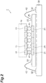
- FIG. 2 is a cross-sectional view illustrating the configuration of the solid-state imaging device 1.
- the solid-state imaging device 1 has a configuration in which a second substrate 20 is disposed on a package 30 and a first substrate 10 is disposed on the second substrate 20.
- a plurality of photodiodes 11 are two-dimensionally arranged and formed on the first substrate 10.
- the photodiode 11 may be made of a compound semiconductor, such as InGaAs, for example.
- a plurality of pixel circuits 21 are two-dimensionally arranged and formed on the second substrate 20.
- the pixel circuit 21 may be made of silicon.
- the photodiodes 11 and CTIAs 50 (to be described below) of the pixel circuits 21 have a one-to-one correspondence. That is, the CTIA 50 is provided for each pixel.
- the first substrate 10 and the second substrate 20 are disposed to face each other, and the photodiode 11 and the pixel circuit 21 corresponding to each other are electrically connected to each other by a bump 41. Via the bump 41, each photodiode 11 is supplied with a reference voltage, and outputs charges generated according to the amount of incident light to the pixel circuit 21.
- Electrodes 22 formed on the second substrate 20 and electrodes 32 formed on the package 30 are electrically connected to each other by bonding wires 42. Via the bonding wire 42, each pixel circuit 21 is supplied with a reference voltage and a control signal, and outputs results of receiving charges from the photodiode 11 and processing for each pixel.
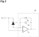
- FIG. 3 is a circuit diagram illustrating a basic configuration of the photodiode 11 and the CTIA 50.
- the CTIA 50 includes a differential amplifier 51, an integration capacitive element 52, and a reset switch 53.
- the differential amplifier 51 includes a non-inverting input terminal (first input terminal), an inverting input terminal (second input terminal), and an output terminal.
- the integration capacitive element 52 and the switch 53 are connected in parallel to each other and are provided between the inverting input terminal and the output terminal of the differential amplifier 51.
- An anode of the photodiode 11 is electrically connected to the inverting input terminal of the differential amplifier 51.
- An inp voltage is input to a cathode of the photodiode 11 and the non-inverting input terminal of the differential amplifier 51. Since the inverting input terminal and the non-inverting input terminal of the differential amplifier 51 are in an imaginary short relationship, a potential difference between the two input terminals is substantially zero. Therefore, since the photodiode 11 is driven with a substantially zero reverse bias voltage, it is possible to suppress a dark current.
- the differential amplifier 51, the integration capacitive element 52, and the switch 53 constitute a capacitive trans-impedance amplifier (CTIA).
- CTIA capacitive trans-impedance amplifier
- the switch 53 When the switch 53 is in an ON state, the integration capacitive element 52 is discharged, and a voltage value output from the output terminal of the differential amplifier 51 becomes an initial value.
- the switch 53 When the switch 53 is in an OFF state, charges are accumulated in the integration capacitive element 52 according to a signal output from the photodiode 11, and a voltage value according to an amount of accumulated charges is output from the output terminal of the differential amplifier 51.
- the switch 53 can be configured by a MOS transistor.
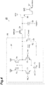
- FIG. 4 is a circuit diagram illustrating a detailed configuration of the pixel circuit 21.
- the pixel circuit 21 illustrated in this figure includes a PMOS transistor 54 as a sampling switch, a capacitive element 55 for sample and hold, an NMOS transistor 56 constituting a source follower circuit, and an NMOS transistor 57 as an output selection switch, in addition to the CTIA 50 including the differential amplifier 51, the integration capacitive element 52, and the switch 53.
- this figure illustrates the circuit configuration of the differential amplifier 51, which will be described below with reference to FIG. 5 .
- a source of the PMOS transistor 54 is connected to the output terminal of the differential amplifier 51.
- a drain of the PMOS transistor 54 is connected to one terminal of the capacitive element 55.
- the other terminal of the capacitive element 55 is set to a reference potential (ground potential).
- an ON/OFF operation between the source and the drain is controlled by a sample signal that is input to a gate.
- the PMOS transistor 54 is changed from an ON state to an OFF state, the voltage value output from the output terminal of the differential amplifier 51 immediately before is held by the capacitive element 55.
- the NMOS transistor 56 and the NMOS transistor 57 are connected in series between a reference potential input terminal and a video line.
- a drain of the NMOS transistor 56 is set to a reference potential (power supply potential Vdd).
- a source of the NMOS transistor 56 is connected to a drain of the NMOS transistor 57.
- a source of the NMOS transistor 57 is connected to the video line.
- the NMOS transistor 56 receives the voltage value held in the capacitive element 55 by a gate, and has a resistance value corresponding to the voltage value between the drain and the source.
- an ON/OFF operation between the source and the drain is controlled by a shift signal that is input to a gate.
- a signal according to the voltage value held in the capacitive element 55 is output to the video line.
- the pixel circuit 21 is provided for each pixel.
- a plurality of pixel circuits 21 are connected to a signal processing circuit by the common video line.
- the respective NMOS transistors 57 of the plurality of pixel circuits 21 connected to the common video line are sequentially turned ON.
- the signal processing circuit selectively receives a signal output from the pixel circuit 21 in which the NMOS transistor 57 is in the ON state among the plurality of pixel circuits 21 connected to the common video line, and processes the input signal.
- FIG. 5 is a circuit diagram of the differential amplifier 51.
- the differential amplifier 51 includes a non-inverting input terminal (first input terminal) 61, an inverting input terminal (second input terminal) 62, and an output terminal 63.
- the differential amplifier 51 includes an input differential pair 66 including an NMOS transistor (first MOS transistor) 71 and an NMOS transistor (second MOS transistor) 72, a current mirror pair 67 including a PMOS transistor (third MOS transistor) 73 and a PMOS transistor (fourth MOS transistor) 74, and a constant current source 68 including an NMOS transistor (fifth MOS transistor) 75.
- the NMOS transistor 71 and the NMOS transistor 72 have the same configuration. Sources of the NMOS transistors 71 and 72 are connected to a common node 64. A gate of the NMOS transistor 71 is connected to the non-inverting input terminal 61. A gate of the NMOS transistor 72 is connected to the inverting input terminal 62.
- the PMOS transistor 73 and the PMOS transistor 74 have the same configuration.
- a first reference voltage (power supply potential Vdd) is input to sources of the PMOS transistors 73 and 74.
- a drain of the PMOS transistor 73 is connected to a drain of the NMOS transistor 71.
- a drain of the PMOS transistor 74 is connected to a drain of the NMOS transistor 72 and the output terminal 63.
- Gates of the PMOS transistors 73 and 74 are connected to the drain of the PMOS transistor 73.
- a second reference voltage (ground potential) is input to a source of the NMOS transistor 75.
- a drain of the NMOS transistor 75 is connected to the common node 64.
- a third reference voltage (bias voltage vb1) is input to a gate of the NMOS transistor 75.
- a threshold voltage of each of the NMOS transistors 71 and 72 is higher than a threshold voltage of the NMOS transistor 75.
- the above configuration is also suitable for reduction in a pitch of the pixel circuit 21 including the differential amplifier 51 since a circuit scale (the number of transistors) of the differential amplifier 51 does not change.
- the threshold voltage of each of the NMOS transistors 71 and 72 is higher than threshold voltages of other NMOS transistors (specifically, the NMOS transistor (sixth MOS transistor) 56 and the NMOS transistor (seventh MOS transistor) 57) other than the NMOS transistor 75 included in the pixel circuit 21.
- the above configuration is also suitable for reduction in a pitch of the pixel circuit 21 including the differential amplifier 51 since a circuit scale (the number of transistors) of the differential amplifier 51 does not change.
- a voltage value of the common node 64 is denoted by p1.
- An input voltage value of the non-inverting input terminal 61 is denoted by inp.
- the threshold voltage is denoted by V th .
- a gate width is denoted by W.
- a gate length is denoted by L.
- a drain current is denoted by I d .
- a carrier mobility is denoted by ⁇ .
- a capacitance value per unit area of an insulating layer under the gate is denoted by C ox .
- a work function of the gate is denoted by ⁇ G .
- a work function of a semiconductor is denoted by ⁇ S .
- a permittivity of the semiconductor is denoted by ⁇ s .
- An elementary charge is denoted by q.
- An impurity concentration in a channel region under the gate is denoted by N A .
- a Fermi potential is denoted by ⁇ P .
- Formula (1) inp ⁇ V th ⁇ 2 L ⁇ I d W ⁇ ⁇ ⁇ C OX
- V th ⁇ G ⁇ ⁇ S + 2 ⁇ s ⁇ q ⁇ N A ⁇ 2 ⁇ P C ox + 2 ⁇ P
- the voltage value output from the output terminal 63 of the differential amplifier 51 is limited to a range from the input voltage value inp of the non-inverting input terminal 61 to the voltage value p1 of the common node 64. Therefore, since the voltage value p1 of the common node 64 can be reduced when the threshold voltage V th of each of the NMOS transistors 71 and 72 is increased, it is possible to increase the output range of the differential amplifier 51.
- the impurity concentration N A in the channel region may be increased in order to increase the threshold voltage V th . That is, the impurity concentration N A in the channel region under the gate of the NMOS transistor for which the threshold voltage V th is to be increased may be set to be higher than those of the other NMOS transistors.
- a conductivity type or an impurity concentration may be different between the gate of the NMOS transistor for which the threshold voltage V th is to be increased and the gate of the other NMOS transistor. That is, a difference ( ⁇ G - ⁇ S ) between the work function ⁇ G of the gate and the work function ⁇ S of the semiconductor in the above Formula (2) depends on the conductivity type and the impurity concentration of the gate. It is possible to increase the threshold voltage V th by increasing this difference ( ⁇ G - ⁇ S ).
- a polysilicon is used as a gate material.
- the NMOS transistor it is possible to increase the threshold voltage V th by changing the gate made of polysilicon from the N-type to the P-type.
- the gate of the NMOS transistor is of the N-type, it is possible to increase the threshold voltage V th by reducing the impurity concentration.
- the gate of the NMOS transistor is of the P-type, it is possible to increase the threshold voltage V th by increasing the impurity concentration.
- the threshold voltage V th by changing the gate made of polysilicon from the P-type to the N-type.
- the gate of the PMOS transistor is of the N-type, it is possible to increase the threshold voltage V th by increasing the impurity concentration.
- the gate of the PMOS transistor is of the P-type, it is possible to increase the threshold voltage V th by reducing the impurity concentration.
- the capacitance value C ox per unit area of the insulating layer under the gate of the NMOS transistor for which the threshold voltage V th is to be increased may be decreased.
- a material having a low relative permittivity may be used as the insulating layer under the gate, or the insulating layer may be thickened, in order to increase the threshold voltage V th .
- the threshold voltage of the NMOS transistor 75 may be higher than the threshold voltages of the NMOS transistors 56 and 57.
- the respective threshold voltages of the NMOS transistors 71, 72, and 75 may be approximately the same.
- a current I flowing through the NMOS transistor 75 is expressed by the following Formula (3) using a voltage V gs between the gate and the source of the NMOS transistor 75, that is, the bias voltage vb1.
- V gs between the gate and the source of the NMOS transistor 75 that is, the bias voltage vb1.
- the bias voltage vb1 is also increased so that the difference (V gs -V th ) does not change, the current I can also be kept unchanged.
- FIG. 6 is a diagram illustrating a configuration of a circuit used in a simulation.
- a simulation circuit illustrated in this figure uses a constant current source 11A in place of the photodiode 11 in the circuit illustrated in FIG. 3 . That is, this constant current source 11A imitates a photodiode that generates a constant amount of charges over time.
- FIG. 7 is a graph illustrating the simulation results.
- Two cases A and B were assumed for the simulation.
- the respective threshold voltages of the NMOS transistors 71, 72, 75, 56, and 57 were set to 0.65 V.
- the respective threshold voltages of the NMOS transistors 71 and 72 were set to 1.00 V, and the respective threshold voltages of the NMOS transistors 75, 56 and 57 were set to 0.65 V.
- the input voltage value inp of the non-inverting input terminal was set to 2.7 V.
- An output current value of the constant current source 11A was set to 3 nA.
- An ON period of the switch 53 was set to 30 ⁇ s.
- a capacitance value of the integration capacitive element 52 was set to 30 pF.
- the voltage value output from the output terminal of the differential amplifier 51 is from 2.7 V to 1.75 V.
- the voltage value output from the output terminal of the differential amplifier 51 is from 2.7 V to 1.4 V. It is confirmed that the output range is larger in the case B than in the case A. A difference in the output range between the case A and the case B is 0.35 V, which is the same as a difference in the threshold voltage.
- the present invention is not limited to the above embodiment and configuration examples, and various modifications are possible.
- the first conductivity type is the N-type and the second conductivity type is the P-type
- the first conductivity type may be the P-type and the second conductivity type may be the N-type.
- the differential amplifier can also be used in other circuits.
- the differential amplifier according to the above embodiment is a differential amplifier including a first input terminal, a second input terminal, and an output terminal, and includes (1) an input differential pair including a first MOS transistor and a second MOS transistor of a first conductivity type, sources of the first MOS transistor and the second MOS transistor being connected to a common node, a gate of the first MOS transistor being connected to the first input terminal, and a gate of the second MOS transistor being connected to the second input terminal, (2) a current mirror pair including a third MOS transistor and a fourth MOS transistor of a second conductivity type, a first reference voltage being input to sources of the third MOS transistor and the fourth MOS transistor, a drain of the third MOS transistor being connected to a drain of the first MOS transistor, a drain of the fourth MOS transistor being connected to a drain of the second MOS transistor and the output terminal, and gates of the third MOS transistor and the fourth MOS transistor being connected to the drain of the third MOS transistor, and (3) a constant current source including a fifth MOS
- an impurity concentration in a channel region under the gate of each of the first MOS transistor and the second MOS transistor may be higher than an impurity concentration in a channel region under the gate of the fifth MOS transistor.
- a conductivity type or an impurity concentration may be different between the gate of each of the first MOS transistor and the second MOS transistor and the gate of the fifth MOS transistor.
- the pixel circuit according to the above embodiment includes the differential amplifier of the above configuration, and an integration capacitive element provided between the second input terminal and the output terminal of the differential amplifier and for accumulating charges according to a signal input to the second input terminal, and a signal having a value according to an amount of accumulated charges in the integration capacitive element is output from the output terminal of the differential amplifier.
- the solid-state imaging device includes the pixel circuit of the above configuration, and a photodiode, and the pixel circuit inputs a signal output according to light reception from the photodiode to the second input terminal of the differential amplifier, and outputs an output signal having a value according to an amount of received light from the output terminal of the differential amplifier.
- a plurality of photodiodes may be formed on a first substrate, a plurality of pixel circuits may be formed on a second substrate, and the first substrate and the second substrate may be disposed to face each other.
- the pixel circuit includes a differential amplifier including a first input terminal, a second input terminal, and an output terminal, and an integration capacitive element provided between the second input terminal and the output terminal of the differential amplifier and for accumulating charges according to a signal input to the second input terminal, the pixel circuit outputting a signal having a value according to an amount of accumulated charges in the integration capacitive element from the output terminal of the differential amplifier, and the differential amplifier includes (1) an input differential pair including a first MOS transistor and a second MOS transistor of a first conductivity type, sources of the first MOS transistor and the second MOS transistor being connected to a common node, a gate of the first MOS transistor being connected to the first input terminal, and a gate of the second MOS transistor being connected to the second input terminal, (2) a current mirror pair including a third MOS transistor and a fourth MOS transistor of a second conductivity type, a first reference voltage being input to sources of the third MOS transistor and the fourth MOS transistor, a drain of the third MOS
- an impurity concentration in a channel region under the gate of each of the first MOS transistor and the second MOS transistor may be higher than an impurity concentration in a channel region under the gate of the other MOS transistor.
- a conductivity type or an impurity concentration may be different between the gate of each of the first MOS transistor and the second MOS transistor and the gate of the other MOS transistor.
- a threshold voltage of the fifth MOS transistor may be higher than the threshold voltage of the other MOS transistor.
- an impurity concentration in a channel region under the gate of the fifth MOS transistor may be higher than an impurity concentration in a channel region under the gate of the other MOS transistor.
- a conductivity type or an impurity concentration may be different between the gate of the fifth MOS transistor and the gate of the other MOS transistor.
- the pixel circuit of the above configuration may be configured to include, as the other MOS transistor, a sixth MOS transistor of the first conductivity type including a gate to which a signal output from the output terminal of the differential amplifier is input and constituting a source follower circuit, and a seventh MOS transistor of the first conductivity type connected in series with the sixth MOS transistor.
- the solid-state imaging device includes the pixel circuit of the above configuration, and a photodiode, and the pixel circuit inputs a signal output according to light reception from the photodiode to the second input terminal of the differential amplifier, and outputs an output signal having a value according to an amount of received light from the output terminal of the differential amplifier.
- a plurality of photodiodes may be formed on a first substrate, a plurality of pixel circuits may be formed on a second substrate, and the first substrate and the second substrate may be disposed to face each other.
- the present invention can be used as a differential amplifier, a pixel circuit, and a solid-state imaging device capable of reducing a pitch of the pixel circuits and suppressing decrease in an output range.
- 1 - solid-state imaging device 10 - first substrate, 11 - photodiode, 20 - second substrate, 21 - pixel circuit, 22 - electrode, 30 - package, 32 - electrode, 41 - bump, 42 - bonding wire, 50 - CTIA, 51 - differential amplifier, 52 - integration capacitive element, 53 - switch, 54 - PMOS transistor, 55 - capacitive element, 56 - NMOS transistor (sixth MOS transistor), 57 - NMOS transistor (seventh MOS transistor), 61 - non-inverting input terminal (first input terminal), 62 - inverting input terminal (second input terminal), 63 - output terminal, 64 - common node, 66 - input differential pair, 67 - current mirror pair, 68 - constant current source, 71 - NMOS transistor (first MOS transistor), 72 - NMOS transistor (second MOS transistor), 73 - PMOS transistor (third MOS transistor), 74 - PMOS transistor (fourth
Landscapes
- Engineering & Computer Science (AREA)
- Power Engineering (AREA)
- Multimedia (AREA)
- Signal Processing (AREA)
- Transforming Light Signals Into Electric Signals (AREA)
- Solid State Image Pick-Up Elements (AREA)
- Amplifiers (AREA)
Abstract
Description
- The present invention relates to a differential amplifier, a pixel circuit including the differential amplifier, and a solid-state imaging device including the pixel circuit.
- In general, a solid-state imaging device includes a plurality of photodiodes arranged and formed in a one-dimensional or two-dimensional form on a substrate, and a pixel circuit that receives and processes output signals from the plurality of photodiodes. Further, the pixel circuit includes an amplifier and an integration capacitive element. The pixel circuit receives a signal output from the photodiode, accumulates charges in the integration capacitive element, and outputs a voltage value according to an amount of accumulated charges from an output terminal of the amplifier.
- A differential amplifier (see Patent Document 1) is used as the amplifier in the pixel circuit. In this case, a reference voltage is input to a first input terminal of the differential amplifier, and a signal from the photodiode is input to a second input terminal. In the differential amplifier, since the two input terminals are in an imaginary short relationship, a potential difference between the two input terminals is substantially zero. Therefore, since the photodiode can be driven with a substantially zero reverse bias voltage, it is possible to suppress a dark current. In this respect, it is preferable to use the differential amplifier in the pixel circuit.
- In a solid-state imaging device, high integration of photodiodes is required in order to improve spatial resolution and achieve low price. That is, an increase in the number of photodiodes formed on a substrate and reduction in a pitch of pixels (reduction in an area of each photodiode) are required. In order to achieve the high integration, the solid-state imaging device may have a configuration in which a first substrate on which a plurality of photodiodes are formed and a second substrate on which a plurality of pixel circuits are formed are disposed to face each other. In particular, when photodiodes are formed on the first substrate made of a compound semiconductor and pixel circuits are formed on the second substrate made of silicon, the first substrate and the second substrate are separated from each other. In this case, high integration of the pixel circuits on the second substrate is also required together with high integration of the photodiodes on the first substrate. That is, reduction in a pitch of the pixel circuit on the second substrate (reduction in an area of a layout of each pixel circuit) is also required.
- Patent Document 1: Japanese Patent Application Laid-Open Publication No.
H6-216666 - The present inventors have obtained the following knowledge in a process of conducting research on reduction in a pitch of a pixel circuit including a differential amplifier. That is, a magnitude of an output range of the differential amplifier is limited by a circuit configuration of the differential amplifier. In order to increase the output range, it may be possible to modify a circuit, such as to provide an output buffer after the differential amplifier as described in Patent Document 1. However, in this case, a circuit scale of the pixel circuit including the differential amplifier becomes large, which is contrary to the purpose of reduction in the pitch of the pixel circuit.
- Further, it is necessary to manufacture the pixel circuit using a fine CMOS process in order to reduce the pitch of the pixel circuit. However, since a differential amplifier manufactured by the fine CMOS process is driven by a low power supply voltage, the output range of the differential amplifier is reduced accordingly.
- The present invention has been made on the basis of the above knowledge of the present inventors, and an object thereof is to provide a differential amplifier, a pixel circuit, and a solid-state imaging device capable of reducing a pitch of the pixel circuit and suppressing decrease in an output range.
- A differential amplifier according to the present invention is a differential amplifier including a first input terminal, a second input terminal, and an output terminal, and includes (1) an input differential pair including a first MOS transistor and a second MOS transistor of a first conductivity type, sources of the first MOS transistor and the second MOS transistor being connected to a common node, a gate of the first MOS transistor being connected to the first input terminal, and a gate of the second MOS transistor being connected to the second input terminal; (2) a current mirror pair including a third MOS transistor and a fourth MOS transistor of a second conductivity type, a first reference voltage being input to sources of the third MOS transistor and the fourth MOS transistor, a drain of the third MOS transistor being connected to a drain of the first MOS transistor, a drain of the fourth MOS transistor being connected to a drain of the second MOS transistor and the output terminal, and gates of the third MOS transistor and the fourth MOS transistor being connected to the drain of the third MOS transistor; and (3) a constant current source including a fifth MOS transistor of the first conductivity type, a second reference voltage being input to a source of the fifth MOS transistor, a drain of the fifth MOS transistor being connected to the common node, and a third reference voltage being input to a gate of the fifth MOS transistor, and (4) a threshold voltage of each of the first MOS transistor and the second MOS transistor is higher than a threshold voltage of the fifth MOS transistor.
- Further, one of the first conductivity type and the second conductivity type is an N-type, and the other is a P-type. One of the first reference voltage and the second reference voltage is a power supply potential Vdd, and the other is a ground potential. The third reference voltage is a potential that is applied to the gate of the fifth MOS transistor in order to use the fifth MOS transistor as a constant current source.
- A pixel circuit according to the present invention includes the differential amplifier of the above configuration; and an integration capacitive element provided between the second input terminal and the output terminal of the differential amplifier and for accumulating charges according to a signal input to the second input terminal, and a signal having a value according to an amount of accumulated charges in the integration capacitive element is output from the output terminal of the differential amplifier.
- A solid-state imaging device according to the present invention includes the pixel circuit of the above configuration; and a photodiode, and the pixel circuit inputs a signal output according to light reception from the photodiode to the second input terminal of the differential amplifier, and outputs an output signal having a value according to an amount of received light from the output terminal of the differential amplifier.
- A pixel circuit according to the present invention includes a differential amplifier including a first input terminal, a second input terminal, and an output terminal; and an integration capacitive element provided between the second input terminal and the output terminal of the differential amplifier and for accumulating charges according to a signal input to the second input terminal, the pixel circuit outputting a signal having a value according to an amount of accumulated charges in the integration capacitive element from the output terminal of the differential amplifier, and the differential amplifier includes (1) an input differential pair including a first MOS transistor and a second MOS transistor of a first conductivity type, sources of the first MOS transistor and the second MOS transistor being connected to a common node, a gate of the first MOS transistor being connected to the first input terminal, and a gate of the second MOS transistor being connected to the second input terminal; (2) a current mirror pair including a third MOS transistor and a fourth MOS transistor of a second conductivity type, a first reference voltage being input to sources of the third MOS transistor and the fourth MOS transistor, a drain of the third MOS transistor being connected to a drain of the first MOS transistor, a drain of the fourth MOS transistor being connected to a drain of the second MOS transistor and the output terminal, and gates of the third MOS transistor and the fourth MOS transistor being connected to the drain of the third MOS transistor; and (3) a constant current source including a fifth MOS transistor of the first conductivity type, a second reference voltage being input to a source of the fifth MOS transistor, a drain of the fifth MOS transistor being connected to the common node, and a third reference voltage being input to a gate of the fifth MOS transistor, and (4) a threshold voltage of each of the first MOS transistor and the second MOS transistor is higher than a threshold voltage of another MOS transistor of the first conductivity type other than the fifth MOS transistor included in the pixel circuit.
- Further, one of the first conductivity type and the second conductivity type is an N-type, and the other is a P-type. One of the first reference voltage and the second reference voltage is a power supply potential Vdd, and the other is a ground potential. The third reference voltage is a potential that is applied to the gate of the fifth MOS transistor in order to use the fifth MOS transistor as a constant current source.
- A solid-state imaging device according to the present invention includes the pixel circuit of the above configuration; and a photodiode, and the pixel circuit inputs a signal output according to light reception from the photodiode to the second input terminal of the differential amplifier, and outputs an output signal having a value according to an amount of received light from the output terminal of the differential amplifier.
- According to the present invention, it is possible to reduce a pitch of the pixel circuit and to suppress decrease in the output range of the differential amplifier.
-
- [
FIG. 1] FIG. 1 is a perspective view illustrating a configuration of a solid-state imaging device 1. - [
FIG. 2] FIG. 2 is a cross-sectional view illustrating the configuration of the solid-state imaging device 1. - [
FIG. 3] FIG. 3 is a circuit diagram illustrating a basic configuration of aphotodiode 11 and a CTIA 50. - [
FIG. 4] FIG 4 is a circuit diagram illustrating a detailed configuration of apixel circuit 21. - [
FIG. 5] FIG. 5 is a circuit diagram of adifferential amplifier 51. - [
FIG. 6] FIG. 6 is a diagram illustrating a configuration of a circuit used in a simulation. - [
FIG. 7] FIG. 7 is a graph illustrating simulation results. - Hereinafter, embodiments for carrying out the present invention will be described in detail with reference to the accompanying drawings. In the description of the drawings, the same elements will be denoted by the same reference signs, without redundant description. The present invention is not limited to these examples.
-
FIG. 1 is a perspective view illustrating a configuration of a solid-state imaging device 1.FIG. 2 is a cross-sectional view illustrating the configuration of the solid-state imaging device 1. The solid-state imaging device 1 has a configuration in which asecond substrate 20 is disposed on apackage 30 and afirst substrate 10 is disposed on thesecond substrate 20. A plurality ofphotodiodes 11 are two-dimensionally arranged and formed on thefirst substrate 10. Thephotodiode 11 may be made of a compound semiconductor, such as InGaAs, for example. A plurality ofpixel circuits 21 are two-dimensionally arranged and formed on thesecond substrate 20. Thepixel circuit 21 may be made of silicon. - The
photodiodes 11 and CTIAs 50 (to be described below) of thepixel circuits 21 have a one-to-one correspondence. That is, the CTIA 50 is provided for each pixel. Thefirst substrate 10 and thesecond substrate 20 are disposed to face each other, and thephotodiode 11 and thepixel circuit 21 corresponding to each other are electrically connected to each other by abump 41. Via thebump 41, eachphotodiode 11 is supplied with a reference voltage, and outputs charges generated according to the amount of incident light to thepixel circuit 21.Electrodes 22 formed on thesecond substrate 20 andelectrodes 32 formed on thepackage 30 are electrically connected to each other by bondingwires 42. Via thebonding wire 42, eachpixel circuit 21 is supplied with a reference voltage and a control signal, and outputs results of receiving charges from thephotodiode 11 and processing for each pixel. -
FIG. 3 is a circuit diagram illustrating a basic configuration of thephotodiode 11 and theCTIA 50. TheCTIA 50 includes adifferential amplifier 51, anintegration capacitive element 52, and areset switch 53. Thedifferential amplifier 51 includes a non-inverting input terminal (first input terminal), an inverting input terminal (second input terminal), and an output terminal. Theintegration capacitive element 52 and theswitch 53 are connected in parallel to each other and are provided between the inverting input terminal and the output terminal of thedifferential amplifier 51. An anode of thephotodiode 11 is electrically connected to the inverting input terminal of thedifferential amplifier 51. An inp voltage is input to a cathode of thephotodiode 11 and the non-inverting input terminal of thedifferential amplifier 51. Since the inverting input terminal and the non-inverting input terminal of thedifferential amplifier 51 are in an imaginary short relationship, a potential difference between the two input terminals is substantially zero. Therefore, since thephotodiode 11 is driven with a substantially zero reverse bias voltage, it is possible to suppress a dark current. - The
differential amplifier 51, theintegration capacitive element 52, and theswitch 53 constitute a capacitive trans-impedance amplifier (CTIA). When theswitch 53 is in an ON state, theintegration capacitive element 52 is discharged, and a voltage value output from the output terminal of thedifferential amplifier 51 becomes an initial value. When theswitch 53 is in an OFF state, charges are accumulated in theintegration capacitive element 52 according to a signal output from thephotodiode 11, and a voltage value according to an amount of accumulated charges is output from the output terminal of thedifferential amplifier 51. In addition, theswitch 53 can be configured by a MOS transistor. -
FIG. 4 is a circuit diagram illustrating a detailed configuration of thepixel circuit 21. Thepixel circuit 21 illustrated in this figure includes aPMOS transistor 54 as a sampling switch, acapacitive element 55 for sample and hold, anNMOS transistor 56 constituting a source follower circuit, and anNMOS transistor 57 as an output selection switch, in addition to theCTIA 50 including thedifferential amplifier 51, theintegration capacitive element 52, and theswitch 53. In addition, this figure illustrates the circuit configuration of thedifferential amplifier 51, which will be described below with reference toFIG. 5 . - A source of the
PMOS transistor 54 is connected to the output terminal of thedifferential amplifier 51. A drain of thePMOS transistor 54 is connected to one terminal of thecapacitive element 55. The other terminal of thecapacitive element 55 is set to a reference potential (ground potential). In thePMOS transistor 54, an ON/OFF operation between the source and the drain is controlled by a sample signal that is input to a gate. When thePMOS transistor 54 is changed from an ON state to an OFF state, the voltage value output from the output terminal of thedifferential amplifier 51 immediately before is held by thecapacitive element 55. - The
NMOS transistor 56 and theNMOS transistor 57 are connected in series between a reference potential input terminal and a video line. A drain of theNMOS transistor 56 is set to a reference potential (power supply potential Vdd). A source of theNMOS transistor 56 is connected to a drain of theNMOS transistor 57. A source of theNMOS transistor 57 is connected to the video line. TheNMOS transistor 56 receives the voltage value held in thecapacitive element 55 by a gate, and has a resistance value corresponding to the voltage value between the drain and the source. In theNMOS transistor 57, an ON/OFF operation between the source and the drain is controlled by a shift signal that is input to a gate. When theNMOS transistor 57 enters an ON state, a signal according to the voltage value held in thecapacitive element 55 is output to the video line. - The
pixel circuit 21 is provided for each pixel. A plurality ofpixel circuits 21 are connected to a signal processing circuit by the common video line. Therespective NMOS transistors 57 of the plurality ofpixel circuits 21 connected to the common video line are sequentially turned ON. The signal processing circuit selectively receives a signal output from thepixel circuit 21 in which theNMOS transistor 57 is in the ON state among the plurality ofpixel circuits 21 connected to the common video line, and processes the input signal. -
FIG. 5 is a circuit diagram of thedifferential amplifier 51. Thedifferential amplifier 51 includes a non-inverting input terminal (first input terminal) 61, an inverting input terminal (second input terminal) 62, and anoutput terminal 63. Thedifferential amplifier 51 includes an inputdifferential pair 66 including an NMOS transistor (first MOS transistor) 71 and an NMOS transistor (second MOS transistor) 72, acurrent mirror pair 67 including a PMOS transistor (third MOS transistor) 73 and a PMOS transistor (fourth MOS transistor) 74, and a constantcurrent source 68 including an NMOS transistor (fifth MOS transistor) 75. - The
NMOS transistor 71 and theNMOS transistor 72 have the same configuration. Sources of theNMOS transistors common node 64. A gate of theNMOS transistor 71 is connected to thenon-inverting input terminal 61. A gate of theNMOS transistor 72 is connected to the invertinginput terminal 62. - The
PMOS transistor 73 and thePMOS transistor 74 have the same configuration. A first reference voltage (power supply potential Vdd) is input to sources of thePMOS transistors PMOS transistor 73 is connected to a drain of theNMOS transistor 71. A drain of thePMOS transistor 74 is connected to a drain of theNMOS transistor 72 and theoutput terminal 63. Gates of thePMOS transistors PMOS transistor 73. - A second reference voltage (ground potential) is input to a source of the
NMOS transistor 75. A drain of theNMOS transistor 75 is connected to thecommon node 64. A third reference voltage (bias voltage vb1) is input to a gate of theNMOS transistor 75. - In the
differential amplifier 51 having the above circuit configuration, a threshold voltage of each of theNMOS transistors NMOS transistor 75. - In this way, it is possible to suppress decrease in the output range of the
differential amplifier 51 even when the power supply voltage is decreased due to adoption of the fine CMOS process. Further, the above configuration is also suitable for reduction in a pitch of thepixel circuit 21 including thedifferential amplifier 51 since a circuit scale (the number of transistors) of thedifferential amplifier 51 does not change. - Further, in the
pixel circuit 21 having the above circuit configuration, the threshold voltage of each of theNMOS transistors NMOS transistor 75 included in thepixel circuit 21. - In this way, it is possible to suppress decrease in the output range of the
differential amplifier 51 even when the power supply voltage is decreased due to adoption of the fine CMOS process. Further, the above configuration is also suitable for reduction in a pitch of thepixel circuit 21 including thedifferential amplifier 51 since a circuit scale (the number of transistors) of thedifferential amplifier 51 does not change. - Next, a reason for decrease in the output range of the
differential amplifier 51 being suppressed by making the threshold voltage of each of theNMOS transistors - Various parameters and the like of the NMOS transistors are as follows. A voltage value of the
common node 64 is denoted by p1. An input voltage value of thenon-inverting input terminal 61 is denoted by inp. The threshold voltage is denoted by Vth. A gate width is denoted by W. A gate length is denoted by L. A drain current is denoted by Id. A carrier mobility is denoted by µ. A capacitance value per unit area of an insulating layer under the gate is denoted by Cox. A work function of the gate is denoted by ΦG. A work function of a semiconductor is denoted by ΦS. A permittivity of the semiconductor is denoted by εs. An elementary charge is denoted by q. An impurity concentration in a channel region under the gate is denoted by NA. Further, a Fermi potential is denoted by φP. Between these parameters, there is a relationship of the following Formula (1) and Formula (2).
[Formula 1]
[Formula 2]
- The voltage value output from the
output terminal 63 of thedifferential amplifier 51 is limited to a range from the input voltage value inp of thenon-inverting input terminal 61 to the voltage value p1 of thecommon node 64. Therefore, since the voltage value p1 of thecommon node 64 can be reduced when the threshold voltage Vth of each of theNMOS transistors differential amplifier 51. - The impurity concentration NA in the channel region may be increased in order to increase the threshold voltage Vth. That is, the impurity concentration NA in the channel region under the gate of the NMOS transistor for which the threshold voltage Vth is to be increased may be set to be higher than those of the other NMOS transistors.
- Further, a conductivity type or an impurity concentration may be different between the gate of the NMOS transistor for which the threshold voltage Vth is to be increased and the gate of the other NMOS transistor. That is, a difference (ΦG-ΦS) between the work function ΦG of the gate and the work function ΦS of the semiconductor in the above Formula (2) depends on the conductivity type and the impurity concentration of the gate. It is possible to increase the threshold voltage Vth by increasing this difference (ΦG-ΦS). In addition, in general, a polysilicon is used as a gate material.
- In the case of the NMOS transistor, it is possible to increase the threshold voltage Vth by changing the gate made of polysilicon from the N-type to the P-type. When the gate of the NMOS transistor is of the N-type, it is possible to increase the threshold voltage Vth by reducing the impurity concentration. When the gate of the NMOS transistor is of the P-type, it is possible to increase the threshold voltage Vth by increasing the impurity concentration. On the other hand, in the case of the PMOS transistor, it is possible to increase the threshold voltage Vth by changing the gate made of polysilicon from the P-type to the N-type. When the gate of the PMOS transistor is of the N-type, it is possible to increase the threshold voltage Vth by increasing the impurity concentration. When the gate of the PMOS transistor is of the P-type, it is possible to increase the threshold voltage Vth by reducing the impurity concentration.
- Further, the capacitance value Cox per unit area of the insulating layer under the gate of the NMOS transistor for which the threshold voltage Vth is to be increased may be decreased. Specifically, a material having a low relative permittivity may be used as the insulating layer under the gate, or the insulating layer may be thickened, in order to increase the threshold voltage Vth.
- Further, the threshold voltage of the
NMOS transistor 75 may be higher than the threshold voltages of theNMOS transistors NMOS transistors NMOS transistor 75 is expressed by the following Formula (3) using a voltage Vgs between the gate and the source of theNMOS transistor 75, that is, the bias voltage vb1. As can be seen from this formula, when values of other parameters are the same, and the threshold voltage Vth of theNMOS transistor 75 is high, the current I decreases. However, when the bias voltage vb1 is also increased so that the difference (Vgs-Vth) does not change, the current I can also be kept unchanged. That is, in the case in which the threshold voltage Vth of theNMOS transistor 75 is increased, it is possible to suppress decrease in the output range of thedifferential amplifier 51 when the bias voltage vb1 is increased. In addition, a magnitude of the bias voltage vb1 can be arbitrarily set according to a circuit design. A specific method of increasing the threshold voltage of theNMOS transistor 75 is as described above.
[Formula 3]
- Next, simulation results will be described.
FIG. 6 is a diagram illustrating a configuration of a circuit used in a simulation. A simulation circuit illustrated in this figure uses a constantcurrent source 11A in place of thephotodiode 11 in the circuit illustrated inFIG. 3 . That is, this constantcurrent source 11A imitates a photodiode that generates a constant amount of charges over time. -
FIG. 7 is a graph illustrating the simulation results. Two cases A and B were assumed for the simulation. In the case A, the respective threshold voltages of theNMOS transistors NMOS transistors NMOS transistors current source 11A was set to 3 nA. An ON period of theswitch 53 was set to 30 µs. A capacitance value of theintegration capacitive element 52 was set to 30 pF. - In the case A in which the threshold voltages of the
NMOS transistors differential amplifier 51 is from 2.7 V to 1.75 V. In the case B in which the threshold voltages of theNMOS transistors differential amplifier 51 is from 2.7 V to 1.4 V. It is confirmed that the output range is larger in the case B than in the case A. A difference in the output range between the case A and the case B is 0.35 V, which is the same as a difference in the threshold voltage. - The present invention is not limited to the above embodiment and configuration examples, and various modifications are possible. For example, in the above embodiment, the first conductivity type is the N-type and the second conductivity type is the P-type, and on the other hand, the first conductivity type may be the P-type and the second conductivity type may be the N-type.
- Further, although the case in which the differential amplifier is used as one component of the pixel circuit in the solid-state imaging device has been described in the above embodiment, the differential amplifier can also be used in other circuits.
- The differential amplifier according to the above embodiment is a differential amplifier including a first input terminal, a second input terminal, and an output terminal, and includes (1) an input differential pair including a first MOS transistor and a second MOS transistor of a first conductivity type, sources of the first MOS transistor and the second MOS transistor being connected to a common node, a gate of the first MOS transistor being connected to the first input terminal, and a gate of the second MOS transistor being connected to the second input terminal, (2) a current mirror pair including a third MOS transistor and a fourth MOS transistor of a second conductivity type, a first reference voltage being input to sources of the third MOS transistor and the fourth MOS transistor, a drain of the third MOS transistor being connected to a drain of the first MOS transistor, a drain of the fourth MOS transistor being connected to a drain of the second MOS transistor and the output terminal, and gates of the third MOS transistor and the fourth MOS transistor being connected to the drain of the third MOS transistor, and (3) a constant current source including a fifth MOS transistor of the first conductivity type, a second reference voltage being input to a source of the fifth MOS transistor, a drain of the fifth MOS transistor being connected to the common node, and a third reference voltage being input to a gate of the fifth MOS transistor, and (4) a threshold voltage of each of the first MOS transistor and the second MOS transistor is higher than a threshold voltage of the fifth MOS transistor.
- In the differential amplifier of the above configuration, an impurity concentration in a channel region under the gate of each of the first MOS transistor and the second MOS transistor may be higher than an impurity concentration in a channel region under the gate of the fifth MOS transistor.
- Further, in the differential amplifier of the above configuration, a conductivity type or an impurity concentration may be different between the gate of each of the first MOS transistor and the second MOS transistor and the gate of the fifth MOS transistor.
- The pixel circuit according to the above embodiment includes the differential amplifier of the above configuration, and an integration capacitive element provided between the second input terminal and the output terminal of the differential amplifier and for accumulating charges according to a signal input to the second input terminal, and a signal having a value according to an amount of accumulated charges in the integration capacitive element is output from the output terminal of the differential amplifier.
- The solid-state imaging device according to the above embodiment includes the pixel circuit of the above configuration, and a photodiode, and the pixel circuit inputs a signal output according to light reception from the photodiode to the second input terminal of the differential amplifier, and outputs an output signal having a value according to an amount of received light from the output terminal of the differential amplifier.
- In the solid-state imaging device of the above configuration, a plurality of photodiodes may be formed on a first substrate, a plurality of pixel circuits may be formed on a second substrate, and the first substrate and the second substrate may be disposed to face each other.
- The pixel circuit according to the above embodiment includes a differential amplifier including a first input terminal, a second input terminal, and an output terminal, and an integration capacitive element provided between the second input terminal and the output terminal of the differential amplifier and for accumulating charges according to a signal input to the second input terminal, the pixel circuit outputting a signal having a value according to an amount of accumulated charges in the integration capacitive element from the output terminal of the differential amplifier, and the differential amplifier includes (1) an input differential pair including a first MOS transistor and a second MOS transistor of a first conductivity type, sources of the first MOS transistor and the second MOS transistor being connected to a common node, a gate of the first MOS transistor being connected to the first input terminal, and a gate of the second MOS transistor being connected to the second input terminal, (2) a current mirror pair including a third MOS transistor and a fourth MOS transistor of a second conductivity type, a first reference voltage being input to sources of the third MOS transistor and the fourth MOS transistor, a drain of the third MOS transistor being connected to a drain of the first MOS transistor, a drain of the fourth MOS transistor being connected to a drain of the second MOS transistor and the output terminal, and gates of the third MOS transistor and the fourth MOS transistor being connected to the drain of the third MOS transistor, and (3) a constant current source including a fifth MOS transistor of the first conductivity type, a second reference voltage being input to a source of the fifth MOS transistor, a drain of the fifth MOS transistor being connected to the common node, and a third reference voltage being input to a gate of the fifth MOS transistor, and (4) a threshold voltage of each of the first MOS transistor and the second MOS transistor is higher than a threshold voltage of another MOS transistor of the first conductivity type other than the fifth MOS transistor included in the pixel circuit.
- In the pixel circuit of the above configuration, an impurity concentration in a channel region under the gate of each of the first MOS transistor and the second MOS transistor may be higher than an impurity concentration in a channel region under the gate of the other MOS transistor.
- Further, in the pixel circuit of the above configuration, a conductivity type or an impurity concentration may be different between the gate of each of the first MOS transistor and the second MOS transistor and the gate of the other MOS transistor.
- In the pixel circuit of the above configuration, a threshold voltage of the fifth MOS transistor may be higher than the threshold voltage of the other MOS transistor. In this case, an impurity concentration in a channel region under the gate of the fifth MOS transistor may be higher than an impurity concentration in a channel region under the gate of the other MOS transistor. Further, a conductivity type or an impurity concentration may be different between the gate of the fifth MOS transistor and the gate of the other MOS transistor.
- The pixel circuit of the above configuration may be configured to include, as the other MOS transistor, a sixth MOS transistor of the first conductivity type including a gate to which a signal output from the output terminal of the differential amplifier is input and constituting a source follower circuit, and a seventh MOS transistor of the first conductivity type connected in series with the sixth MOS transistor.
- The solid-state imaging device according to the above embodiment includes the pixel circuit of the above configuration, and a photodiode, and the pixel circuit inputs a signal output according to light reception from the photodiode to the second input terminal of the differential amplifier, and outputs an output signal having a value according to an amount of received light from the output terminal of the differential amplifier.
- In the solid-state imaging device of the above configuration, a plurality of photodiodes may be formed on a first substrate, a plurality of pixel circuits may be formed on a second substrate, and the first substrate and the second substrate may be disposed to face each other.
- The present invention can be used as a differential amplifier, a pixel circuit, and a solid-state imaging device capable of reducing a pitch of the pixel circuits and suppressing decrease in an output range.
- 1 - solid-state imaging device, 10 - first substrate, 11 - photodiode, 20 - second substrate, 21 - pixel circuit, 22 - electrode, 30 - package, 32 - electrode, 41 - bump, 42 - bonding wire, 50 - CTIA, 51 - differential amplifier, 52 - integration capacitive element, 53 - switch, 54 - PMOS transistor, 55 - capacitive element, 56 - NMOS transistor (sixth MOS transistor), 57 - NMOS transistor (seventh MOS transistor), 61 - non-inverting input terminal (first input terminal), 62 - inverting input terminal (second input terminal), 63 - output terminal, 64 - common node, 66 - input differential pair, 67 - current mirror pair, 68 - constant current source, 71 - NMOS transistor (first MOS transistor), 72 - NMOS transistor (second MOS transistor), 73 - PMOS transistor (third MOS transistor), 74 - PMOS transistor (fourth MOS transistor), 75 - NMOS transistor (fifth MOS transistor).
Claims (15)
- A differential amplifier including a first input terminal, a second input terminal, and an output terminal, the differential amplifier comprising:an input differential pair including a first MOS transistor and a second MOS transistor of a first conductivity type, sources of the first MOS transistor and the second MOS transistor being connected to a common node, a gate of the first MOS transistor being connected to the first input terminal, and a gate of the second MOS transistor being connected to the second input terminal;a current mirror pair including a third MOS transistor and a fourth MOS transistor of a second conductivity type, a first reference voltage being input to sources of the third MOS transistor and the fourth MOS transistor, a drain of the third MOS transistor being connected to a drain of the first MOS transistor, a drain of the fourth MOS transistor being connected to a drain of the second MOS transistor and the output terminal, and gates of the third MOS transistor and the fourth MOS transistor being connected to the drain of the third MOS transistor; anda constant current source including a fifth MOS transistor of the first conductivity type, a second reference voltage being input to a source of the fifth MOS transistor, a drain of the fifth MOS transistor being connected to the common node, and a third reference voltage being input to a gate of the fifth MOS transistor, whereina threshold voltage of each of the first MOS transistor and the second MOS transistor is higher than a threshold voltage of the fifth MOS transistor.
- The differential amplifier according to Claim 1, wherein an impurity concentration in a channel region under the gate of each of the first MOS transistor and the second MOS transistor is higher than an impurity concentration in a channel region under the gate of the fifth MOS transistor.
- The differential amplifier according to Claim 1 or 2, wherein a conductivity type or an impurity concentration is different between the gate of each of the first MOS transistor and the second MOS transistor and the gate of the fifth MOS transistor.
- A pixel circuit comprising:the differential amplifier according to any one of Claims 1 to 3; andan integration capacitive element provided between the second input terminal and the output terminal of the differential amplifier and for accumulating charges according to a signal input to the second input terminal, whereina signal having a value according to an amount of accumulated charges in the integration capacitive element is output from the output terminal of the differential amplifier.
- A solid-state imaging device comprising:the pixel circuit according to Claim 4; anda photodiode, whereinthe pixel circuit inputs a signal output according to light reception from the photodiode to the second input terminal of the differential amplifier, and outputs an output signal having a value according to an amount of received light from the output terminal of the differential amplifier.
- The solid-state imaging device according to Claim 5, wherein a plurality of photodiodes are formed on a first substrate, a plurality of pixel circuits are formed on a second substrate, and the first substrate and the second substrate are disposed to face each other.
- A pixel circuit comprising a differential amplifier including a first input terminal, a second input terminal, and an output terminal; and an integration capacitive element provided between the second input terminal and the output terminal of the differential amplifier and for accumulating charges according to a signal input to the second input terminal, the pixel circuit outputting a signal having a value according to an amount of accumulated charges in the integration capacitive element from the output terminal of the differential amplifier, wherein
the differential amplifier comprises:an input differential pair including a first MOS transistor and a second MOS transistor of a first conductivity type, sources of the first MOS transistor and the second MOS transistor being connected to a common node, a gate of the first MOS transistor being connected to the first input terminal, and a gate of the second MOS transistor being connected to the second input terminal;a current mirror pair including a third MOS transistor and a fourth MOS transistor of a second conductivity type, a first reference voltage being input to sources of the third MOS transistor and the fourth MOS transistor, a drain of the third MOS transistor being connected to a drain of the first MOS transistor, a drain of the fourth MOS transistor being connected to a drain of the second MOS transistor and the output terminal, and gates of the third MOS transistor and the fourth MOS transistor being connected to the drain of the third MOS transistor; anda constant current source including a fifth MOS transistor of the first conductivity type, a second reference voltage being input to a source of the fifth MOS transistor, a drain of the fifth MOS transistor being connected to the common node, and a third reference voltage being input to a gate of the fifth MOS transistor, and whereina threshold voltage of each of the first MOS transistor and the second MOS transistor is higher than a threshold voltage of another MOS transistor of the first conductivity type other than the fifth MOS transistor included in the pixel circuit. - The pixel circuit according to Claim 7, wherein an impurity concentration in a channel region under the gate of each of the first MOS transistor and the second MOS transistor is higher than an impurity concentration in a channel region under the gate of the other MOS transistor.
- The pixel circuit according to Claim 7 or 8, wherein a conductivity type or an impurity concentration is different between the gate of each of the first MOS transistor and the second MOS transistor and the gate of the other MOS transistor.
- The pixel circuit according to any one of Claims 7 to 9, wherein a threshold voltage of the fifth MOS transistor is higher than the threshold voltage of the other MOS transistor.
- The pixel circuit according to Claim 10, wherein an impurity concentration in a channel region under the gate of the fifth MOS transistor is higher than an impurity concentration in a channel region under the gate of the other MOS transistor.
- The pixel circuit according to Claim 10 or 11, wherein a conductivity type or an impurity concentration is different between the gate of the fifth MOS transistor and the gate of the other MOS transistor.
- The pixel circuit according to any one of Claims 7 to 12, comprising, as the other MOS transistor, a sixth MOS transistor of the first conductivity type including a gate to which a signal output from the output terminal of the differential amplifier is input and constituting a source follower circuit, and a seventh MOS transistor of the first conductivity type connected in series with the sixth MOS transistor.
- A solid-state imaging device comprising:the pixel circuit according to any one of Claims 7 to 13; anda photodiode, whereinthe pixel circuit inputs a signal output according to light reception from the photodiode to the second input terminal of the differential amplifier, and outputs an output signal having a value according to an amount of received light from the output terminal of the differential amplifier.
- The solid-state imaging device according to Claim 14, wherein a plurality of photodiodes are formed on a first substrate, a plurality of pixel circuits are formed on a second substrate, and the first substrate and the second substrate are disposed to face each other.
Applications Claiming Priority (3)
| Application Number | Priority Date | Filing Date | Title |
|---|---|---|---|
| JP2017197591A JP6975606B2 (en) | 2017-10-11 | 2017-10-11 | Solid-state image sensor |
| JP2017197592A JP6814122B2 (en) | 2017-10-11 | 2017-10-11 | Pixel circuit and solid-state image sensor |
| PCT/JP2018/037089 WO2019073883A1 (en) | 2017-10-11 | 2018-10-03 | Differential amplifier, pixel circuit and solid-state imaging device |
Publications (2)
| Publication Number | Publication Date |
|---|---|
| EP3696971A1 true EP3696971A1 (en) | 2020-08-19 |
| EP3696971A4 EP3696971A4 (en) | 2021-07-14 |
Family
ID=66100840
Family Applications (1)
| Application Number | Title | Priority Date | Filing Date |
|---|---|---|---|
| EP18866116.9A Pending EP3696971A4 (en) | 2017-10-11 | 2018-10-03 | DIFFERENTIAL AMPLIFIER, PIXEL CIRCUIT AND SEMICONDUCTOR IMAGING DEVICE |
Country Status (5)
| Country | Link |
|---|---|
| US (1) | US11258976B2 (en) |
| EP (1) | EP3696971A4 (en) |
| CN (1) | CN111201708B (en) |
| TW (1) | TWI778145B (en) |
| WO (1) | WO2019073883A1 (en) |
Cited By (1)
| Publication number | Priority date | Publication date | Assignee | Title |
|---|---|---|---|---|
| WO2026006231A1 (en) * | 2024-06-27 | 2026-01-02 | Micron Technology, Inc. | Semiconductor device having differentia amplifier |
Families Citing this family (6)
| Publication number | Priority date | Publication date | Assignee | Title |
|---|---|---|---|---|
| TWI728504B (en) * | 2018-11-13 | 2021-05-21 | 日商索尼半導體解決方案公司 | Solid-state imaging element, solid-state imaging device, and electronic equipment |
| WO2022118538A1 (en) | 2020-12-01 | 2022-06-09 | ソニーセミコンダクタソリューションズ株式会社 | Light receiving element and electronic device |
| CN112738359A (en) * | 2020-12-30 | 2021-04-30 | 长春长光辰芯光电技术有限公司 | CTIA pixel unit |
| CN113055617B (en) * | 2021-05-08 | 2023-05-12 | 长春长光辰芯微电子股份有限公司 | Image Sensor |
| CN115694377A (en) * | 2022-10-17 | 2023-02-03 | 复旦大学 | CTIA type readout circuit matched with two-dimensional light guide type detector |
| CN115855271B (en) * | 2023-02-22 | 2023-05-23 | 昆明钍晶科技有限公司 | Readout circuit with large charge processing capability and infrared thermal imaging instrument |
Family Cites Families (20)
| Publication number | Priority date | Publication date | Assignee | Title |
|---|---|---|---|---|
| US5233180A (en) * | 1990-08-30 | 1993-08-03 | Fuji Electric Co., Ltd. | Light sensor having an integration circuit |
| JPH04120907A (en) | 1990-09-12 | 1992-04-21 | Fujitsu Ltd | Operational amplifier circuit |
| JP3111585B2 (en) | 1991-05-31 | 2000-11-27 | 富士電機株式会社 | Optical sensor device |
| JPH06216666A (en) | 1992-11-30 | 1994-08-05 | Sharp Corp | Differential amplifier |
| JPH07262785A (en) | 1994-03-24 | 1995-10-13 | Nippon Telegr & Teleph Corp <Ntt> | Sense circuit |
| JPH11266398A (en) | 1998-03-16 | 1999-09-28 | Sony Corp | Solid-state imaging device, driving method thereof, and imaging camera |
| KR20010084506A (en) * | 2000-02-26 | 2001-09-06 | 윤종용 | Input buffer circuit of a semiconductor device |
| JP4736313B2 (en) | 2002-09-10 | 2011-07-27 | 日本電気株式会社 | Thin film semiconductor device |
| JP2004266597A (en) * | 2003-03-03 | 2004-09-24 | Shoji Kawahito | Image sensor with full-pixel simultaneous electronic shutter function |
| JP4311181B2 (en) * | 2003-12-05 | 2009-08-12 | ソニー株式会社 | Semiconductor device control method, signal processing method, semiconductor device, and electronic apparatus |
| JP4349232B2 (en) | 2004-07-30 | 2009-10-21 | ソニー株式会社 | Semiconductor module and MOS solid-state imaging device |
| JP4502212B2 (en) * | 2006-01-06 | 2010-07-14 | ルネサスエレクトロニクス株式会社 | Differential amplifier, data driver and display device |
| US7432762B2 (en) | 2006-03-30 | 2008-10-07 | Agere Systems Inc. | Circuit having enhanced input signal range |
| JP4900200B2 (en) * | 2007-11-15 | 2012-03-21 | ソニー株式会社 | Solid-state imaging device and camera system |
| US8310580B2 (en) * | 2009-07-27 | 2012-11-13 | Sony Corporation | Solid-state imaging device and camera system for suppressing occurrence of quantization vertical streaks |
| JP5126305B2 (en) * | 2010-07-02 | 2013-01-23 | 株式会社ニコン | Solid-state image sensor |
| EP2797228B1 (en) | 2013-04-26 | 2016-04-20 | Xenics N.V. | Method for detecting a photocurrent |
| JP6466645B2 (en) * | 2014-03-17 | 2019-02-06 | オリンパス株式会社 | Imaging device |
| US11025241B2 (en) * | 2018-12-20 | 2021-06-01 | Samsung Electronics Co., Ltd. | Comparator circuit and mobile device |
| JP7353783B2 (en) * | 2019-04-16 | 2023-10-02 | キヤノン株式会社 | Imaging device and its control method; Imaging device and its control method |
-
2018
- 2018-10-03 US US16/754,239 patent/US11258976B2/en active Active
- 2018-10-03 WO PCT/JP2018/037089 patent/WO2019073883A1/en not_active Ceased
- 2018-10-03 EP EP18866116.9A patent/EP3696971A4/en active Pending
- 2018-10-03 CN CN201880065787.6A patent/CN111201708B/en active Active
- 2018-10-09 TW TW107135495A patent/TWI778145B/en active
Cited By (1)
| Publication number | Priority date | Publication date | Assignee | Title |
|---|---|---|---|---|
| WO2026006231A1 (en) * | 2024-06-27 | 2026-01-02 | Micron Technology, Inc. | Semiconductor device having differentia amplifier |
Also Published As
| Publication number | Publication date |
|---|---|
| US11258976B2 (en) | 2022-02-22 |
| TWI778145B (en) | 2022-09-21 |
| EP3696971A4 (en) | 2021-07-14 |
| CN111201708B (en) | 2023-08-01 |
| WO2019073883A1 (en) | 2019-04-18 |
| US20200280694A1 (en) | 2020-09-03 |
| CN111201708A (en) | 2020-05-26 |
| TW201929423A (en) | 2019-07-16 |
Similar Documents
| Publication | Publication Date | Title |
|---|---|---|
| US11258976B2 (en) | Differential amplifier, pixel circuit and solid-state imaging device | |
| EP1592068B1 (en) | MOS-type image sensing device | |
| EP3792985B1 (en) | Back-illuminated semiconductor light detecting device | |
| EP2352240A1 (en) | Information acquisition device and optical communication system | |
| US5473183A (en) | Semiconductor device of a first conductivity type which has a first well of a second conductivity type formed therein and a second well of the first conductivity type formed in the first well and a pair of MOSFET formed in the first and second wells | |
| US12342643B2 (en) | Imaging apparatus | |
| US9117724B2 (en) | Solid-state image sensing device | |
| JP6814122B2 (en) | Pixel circuit and solid-state image sensor | |
| US9247173B2 (en) | Imaging apparatus and imaging system | |
| EP3719840A1 (en) | Image capturing device | |
| US20240347562A1 (en) | Imaging device | |
| US9654714B2 (en) | Shared pixel with fixed conversion gain | |
| US10845329B2 (en) | Ion concentration distribution measuring device | |
| US20170180657A1 (en) | Photoelectric conversion device and imaging system | |
| US10999548B2 (en) | Pixel sensing circuit and driving method therefor, image sensor, and electronic device | |
| US9006639B2 (en) | Pixel architecture with the control terminal of a first switch coupled to the control terminal of a second switch and method | |
| US10249671B2 (en) | Low-noise CMOS image sensor | |
| US20160126274A1 (en) | Image pickup apparatus | |
| US20210013801A1 (en) | Charge pump device and image sensor including the same | |
| JP6975606B2 (en) | Solid-state image sensor | |
| US12363460B2 (en) | Solid-state imaging sensor | |
| KR101340839B1 (en) | High-sensitivity cmos image sensor device | |
| KR20050024208A (en) | Solid state image pickup device | |
| JPH08275059A (en) | Light receiving element circuit, light receiving element circuit array, and method of configuring light receiving element circuit | |
| JP3585898B2 (en) | Camera using CCD solid-state imaging device |
Legal Events
| Date | Code | Title | Description |
|---|---|---|---|
| STAA | Information on the status of an ep patent application or granted ep patent |
Free format text: STATUS: THE INTERNATIONAL PUBLICATION HAS BEEN MADE |
|
| PUAI | Public reference made under article 153(3) epc to a published international application that has entered the european phase |
Free format text: ORIGINAL CODE: 0009012 |
|
| STAA | Information on the status of an ep patent application or granted ep patent |
Free format text: STATUS: REQUEST FOR EXAMINATION WAS MADE |
|
| 17P | Request for examination filed |
Effective date: 20200423 |
|
| AK | Designated contracting states |
Kind code of ref document: A1 Designated state(s): AL AT BE BG CH CY CZ DE DK EE ES FI FR GB GR HR HU IE IS IT LI LT LU LV MC MK MT NL NO PL PT RO RS SE SI SK SM TR |
|
| AX | Request for extension of the european patent |
Extension state: BA ME |
|
| DAV | Request for validation of the european patent (deleted) | ||
| DAX | Request for extension of the european patent (deleted) | ||
| A4 | Supplementary search report drawn up and despatched |
Effective date: 20210611 |
|
| RIC1 | Information provided on ipc code assigned before grant |
Ipc: H03F 3/45 20060101AFI20210607BHEP Ipc: H03F 3/08 20060101ALI20210607BHEP Ipc: H04N 5/378 20110101ALI20210607BHEP Ipc: H03F 1/08 20060101ALI20210607BHEP Ipc: H03F 3/70 20060101ALI20210607BHEP |
|
| STAA | Information on the status of an ep patent application or granted ep patent |
Free format text: STATUS: EXAMINATION IS IN PROGRESS |
|
| 17Q | First examination report despatched |
Effective date: 20230307 |