EP3695455B1 - Wellenleiterverbindung mit gleitsymmetrisch positionierten löchern zur vermeidung von leckage - Google Patents
Wellenleiterverbindung mit gleitsymmetrisch positionierten löchern zur vermeidung von leckage Download PDFInfo
- Publication number
- EP3695455B1 EP3695455B1 EP17784629.2A EP17784629A EP3695455B1 EP 3695455 B1 EP3695455 B1 EP 3695455B1 EP 17784629 A EP17784629 A EP 17784629A EP 3695455 B1 EP3695455 B1 EP 3695455B1
- Authority
- EP
- European Patent Office
- Prior art keywords
- flange
- holes
- waveguide
- glide
- end opening
- Prior art date
- Legal status (The legal status is an assumption and is not a legal conclusion. Google has not performed a legal analysis and makes no representation as to the accuracy of the status listed.)
- Active
Links
Images




Classifications
-
- H—ELECTRICITY
- H01—ELECTRIC ELEMENTS
- H01P—WAVEGUIDES; RESONATORS, LINES, OR OTHER DEVICES OF THE WAVEGUIDE TYPE
- H01P1/00—Auxiliary devices
- H01P1/04—Fixed joints
- H01P1/042—Hollow waveguide joints
-
- H—ELECTRICITY
- H01—ELECTRIC ELEMENTS
- H01P—WAVEGUIDES; RESONATORS, LINES, OR OTHER DEVICES OF THE WAVEGUIDE TYPE
- H01P1/00—Auxiliary devices
- H01P1/20—Frequency-selective devices, e.g. filters
- H01P1/2005—Electromagnetic photonic bandgaps [EPB], or photonic bandgaps [PBG]
-
- H—ELECTRICITY
- H01—ELECTRIC ELEMENTS
- H01P—WAVEGUIDES; RESONATORS, LINES, OR OTHER DEVICES OF THE WAVEGUIDE TYPE
- H01P11/00—Apparatus or processes specially adapted for manufacturing waveguides or resonators, lines, or other devices of the waveguide type
- H01P11/001—Manufacturing waveguides or transmission lines of the waveguide type
- H01P11/002—Manufacturing hollow waveguides
-
- H—ELECTRICITY
- H01—ELECTRIC ELEMENTS
- H01P—WAVEGUIDES; RESONATORS, LINES, OR OTHER DEVICES OF THE WAVEGUIDE TYPE
- H01P3/00—Waveguides; Transmission lines of the waveguide type
- H01P3/12—Hollow waveguides
Definitions
- Embodiments herein relate generally to a waveguide assembly for waveguides and methods for producing the same.
- a waveguide is a device or a guide through which electromagnetic currents are guided.
- the waveguide typically comprises a hollow tube or pipe, and is therefore also referred to as a hollow waveguide.
- the hollow tube may be circular, rectangular or have any other suitable shape.
- the waveguide has a hollow centre and conductive walls defining the centre of the waveguide. The diameter of the waveguide and the wavelength of the electromagnetic wave traveling in the waveguide are closely related in a way that if the frequency of the wave is too low, then the electromagnetic wave cannot propagate through the waveguide.
- Hollow waveguides have been widely used as a hardware standard technology for the design of passive microwave components and antenna arrays. They are entirely made of metal and exhibit attractive features like low loss, good isolation properties and high power handling capability. A common application of hollow waveguides is to be used as a standard interconnection interface of high frequency circuits for lab testing purposes. In such cases, the waveguide typically comprises a flange. There are different types of waveguide flanges, and some of them will be described below.
- the surface of a waveguide flange e.g. made of metal
- waveguide flanges provide a texture pattern around the waveguide opening to facilitate the flow of electromagnetic currents between the waveguide joints without leaking energy.
- the choke flange that contains a corrugation that establishes a high impedance condition at the contact point between the flanges that is transformed into a short-circuit at the side-edges of the waveguide opening by using a ⁇ g /4 section.
- ⁇ g represents the guided (g) wavelength ( ⁇ ) of the wave propagating in the parallel plate waveguide region between the two flanges.
- Another waveguide flange type is the so-called pin-flange adapter where a pin surface surrounding the waveguide opening in one of the flanges avoids any possible power loss when screwed together with a smooth waveguide flange in the presence of a gap between the pin-flange and the smooth flange.
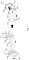
- FIG. 1 An example of a traditional flange of a rectangular waveguide for measurement purposes is illustrated in figure 1 .
- the waveguide is referred to as a rectangular waveguide because the opening has a rectangular shape.
- the left part of figure 1 illustrates a waveguide assembly where three waveguides 101a, 101b, 101c are connected together, and the right part of figure 1 provides a more detailed illustration of some of the flanges comprised in the waveguide assembly.
- Figure 1 illustrates an example where the three waveguides 101a, 101b, 101c are rectangular tubes.
- a first waveguide 101a comprises a first flange 103a surrounding an end opening 105a in one end of the first waveguide 101a.
- a second waveguide 101b comprises a second flange 103b surrounding an end opening 105b in one end of the second waveguide 101b.
- the first waveguide 101a is connected to the second waveguide 101b by connecting the first flange 103a to the second flange 103b so that the end openings 105a, 105b face each other.
- the first and second flange 103a, 103b may be connected to each other by using for example screws or other suitable connecting means.
- figure 1 illustrates that the second waveguide 101b comprises a third flange 103c surrounding an end opening in the opposite end of the second waveguide 101b as compared to the second flange 103b.
- the second waveguide 101b may be a Device Under Test (DUT).
- DUT Device Under Test
- a third waveguide 101c comprises a fourth flange 103d surrounding an end opening of the third waveguide 101c.
- the third waveguide 101c is connected to the second waveguide 101b by connecting the fourth flange 103d to the third flange 103c.
- the end openings 105a, 105b are illustrated as a rectangular openings due to that the waveguide is formed as a rectangular tube.
- each flange 103a, 103b, 103c, 103d are circular flat disks having a smooth surface and having a respective end opening 105a, 105b in the center of the disk.
- Each flange 103a, 103b, 103c, 103d is located around the outer circumference of the end part of the respective waveguide 101a, 101b, 101c.
- the surface of the waveguide flange e.g. made of metal
- Tolerances or errors when mating to flanges 103 can cause gaps 112 between the flange surfaces.
- the errors and gaps 112 can be created by screwing the flanges carelessly or not tightening them well.
- the gaps 112 may cause leakage, reflections and measurement uncertainties.
- Both the flat flange and the choke flange need to be carefully mated so ensure a good electrical contact.
- the term mated may also be described as connected, joined, coupled etc. This is usually done by screwing, which is time consuming and laborious.
- the pin flange and the choke flange both need very accurate fabrication methods, which limits their use at higher frequencies since the dimensions of the corrugations and the pins become very small. Therefore, there is a need to at least mitigate or solve this issue.
- An objective of embodiments herein is therefore to obviate at least one of the above disadvantages and to provide an improved waveguide interconnection.
- the object is achieved by a first waveguide comprising a first flange surrounding an end opening of the first waveguide.
- the first flange comprises at least two holes which are periodically distributed around the end opening.
- the first waveguide is arranged to be connected to a second waveguide by connecting the first flange to a second flange of the second waveguide such that the end opening of the first waveguide faces an end opening of the second waveguide and such that the holes in the first flange are at least partly glide symmetrically positioned with respect to holes which are periodically distributed around the end opening of the second flange.
- the object is achieved by a waveguide assembly for waveguides.
- the waveguide assembly comprises a first waveguide comprising a first flange surrounding an end opening of the first waveguide.
- the waveguide assembly further comprises a second waveguide comprising a second flange surrounding an end opening of the second waveguide.
- Each flange comprises at least two holes which are WO 2014/174494 discloses a system for connecting corrugated wave-guiding modules comprising an asexual, auto aligning, flange with a corrugated structure and screws and/or dowels to prevent the structure to fall outside the flange's inner guiding shape.
- US 2013/342288 discloses a self-keying waveguide interconnection system for repeatable waveguide calibration and connection comprises a plug with a centrally disposed aperture and a jack provided with a counterbore to accept a plug diameter.
- the jack includes a plurality of self-keying channels.
- a shim having a shape complementary to the plurality of self-keying thru slots has a plurality of self-keying thru slots for aligning the centrally disposed aperture of the plug to the centrally disposed aperture of the jack.
- the system identifies the orientation and flange face polarity of the line or adapter without the use of alignment pins as two or more of these independent waveguide interfaces are coupled.
- the device functions as a self-keying shim/spacer/adapter for a calibration kit or adapter in waveguide sections.
- the object is achieved by a method for manufacturing a first waveguide.
- the method comprises providing a first flange surrounding an end opening to the first waveguide.
- the first flange comprises at least two holes which are periodically distributed around the end opening.
- the first waveguide is arranged to be connected to a second waveguide by connecting the first flange to a second flange of the second waveguide such that the end opening of the first waveguide face an end opening of the second waveguide and such that the holes in the first flange are at least partly glide symmetrically positioned with respect to holes which are periodically distributed around the end opening of the second flange.
- the object is achieved by a method for manufacturing a waveguide assembly for waveguides.
- the method comprises providing a first waveguide comprising a first flange surrounding an end opening of the first waveguide.
- the method further comprises providing a second waveguide comprising a second flange surrounding an end opening of the second waveguide.
- Each flange comprises at least two holes which are periodically distributed around the respective end opening.
- the method further comprises connecting the first and second waveguides to each other by connecting the first flange to the second flanges such that the end openings face each other and such that the holes in the first flange are at least partly glide symmetrically positioned with respect to the holes in the second flange.
- each flange comprises at least two holes which are periodically distributed around the respective end opening, and since the first and second waveguides are configured to be connected to each other by connecting the first flange to the second flanges such that the end openings face each other and such that the holes in the first flange are at least partly glide symmetrically positioned with respect to the holes in the second flange.
- a glide symmetric structure is a periodic pattern generated by two geometrical transformations: a translation and a reflection with respect to a certain reference plane. It has been found that by using holes as unit cell of this glide symmetric structure, a wideband stopband where all higher-order modes are avoided is achieved.
- this structure is integrated surrounding a waveguide flange opening, an advantage of the embodiments herein is that any possible leakage of signals with frequencies within the stop band due to a gap between the flange joints is eliminated and a smooth transition is achieved.
- the embodiments herein has an advantage of simplifying the waveguide since it is not necessary to apply several rows of holes in the holey flange configuration as compared to a pin-type flange which has several rows of pins.
- Another advantage of the embodiments herein is that the holes can be made by just drilling, which is much simpler and cost-effective than milling pins or corrugations.
- the depth of the holes is smaller than the pin height in the pin-flange, which should be around ⁇ /4 ( ⁇ represents the wavelength) in order to create an open boundary condition, so the holey flange can be made smaller (thinner) than the pin flange.
- a further advantage of the embodiments herein is that the performance of the at least partly glide symmetric holey structure is insensitive to the flatness of the bottom of the hole, which provides manufacturing flexibility since the drill could have a conical shape and the holey flange still performs as expected.
- the period and hole dimensions in the embodiments herein are larger than the required ones in a pin-type Electromagnetic bandgap (EBG) structure for operating at the same center frequency.
- a larger period means an advantage of less sensitivity to manufacturing tolerances and misalignments. For example, at a center frequency of 60 GHz, it has been seen that misalignments of 0.2 mm do not affect its performance.
- the embodiments herein have an advantage of that both flanges are manufactured identical and when they are joined together the geometry is built-up at least partly glide symmetrically. This fact simplifies the manufacturing and use since there is only one variant of flange.
- the embodiments herein provide the additional advantage of that the at least partly glide symmetric holey flange reduces leakage independently of if the surface of the flange is flat or if it is a bulgy flange.
- the embodiments herein provide the advantage of that the at least partly glide symmetric holey pattern reduces any leakage independently on how the holes are distributed around the waveguide opening (the hole topology can be rounded, elliptical, square etc.).
- the embodiments herein relates to a waveguide with an at least partly glide symmetric holey pattern surrounding the waveguide end opening.
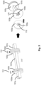
- Figure 2 illustrates an example embodiment of a waveguide assembly.
- a waveguide assembly may be described as waveguides connected to each other via flanges.
- the left part of figure 2 illustrates a waveguide assembly where three waveguides 101a, 101b, 101c are connected together, and the right part of figure 2 provides a more detailed illustration of some of the flanges comprised in the waveguide assembly.
- Figure 2 illustrates an example where the three waveguides 101a, 101b, 101c are hollow tubes having a rectangular form, thus the waveguide can be referred to as a hollow waveguide.
- a first waveguide 101a comprises a first flange 103a surrounding an end opening 105a in one end of the first waveguide 101a.
- a second waveguide 101b comprises a second flange 103b surrounding an end opening 105b in one end of the second waveguide 101b.
- the first waveguide 101a is connected to the second waveguide 101b by connecting the first flange 103a to the second flange 103b so that the end openings face each other.
- figure 2 illustrates that the second waveguide 101b comprises a third flange 103c surrounding an end opening in the opposite end of the second waveguide 101b as compared to the second flange 103b.
- the second waveguide 101b may be a DUT.
- a third waveguide 101c comprises a fourth flange 103d surrounding and end opening (not shown) of the third waveguide 101c.
- the third waveguide 101c is connected to the second waveguide 101b by connecting the fourth flange 103d to the third flange 103c.
- the end openings 105a, 105b are illustrated as a rectangular opening due to that the waveguides 101a, 101b, 101c are formed as rectangular tubes. However, any other suitable shape of the waveguide is applicable such as e.g. a circular tube.
- the end openings 105a, 105b have a shape which corresponds to the shape of the waveguide (i.e. the tube which the waveguide is comprised of).
- the reference number 101 When the reference number 101 is used without the letters a, b or c, it refers to any of the waveguides in the assembly. When the reference number 103 is used without the letters a, b, c or d, it refers to any of the flanges in any of the waveguides 101. Similarly, when the reference number 105 is used without the letters a or b, it refers to any of the end openings in any of the waveguides 101.
- the two waveguides 101 are connected to each other (e.g. the first waveguide 101a and the second waveguide 101b) in an at least partly glide symmetrical way.
- the holes 110 in the first flange 103a are not directly placed opposite to the holes 110 in the second flange 103b when they are connected, but the holes 110 in the first flange 103a at least partly overlap with the holes 110 in the second flange 103b.
- the holes 110 in one flange 103 can glide a certain period with respect to the holes 110 in the other flange 103 when they are connected, e.g.
- the at least partly glide symmetric refers to that the structure may be completely glide symmetric, or quasi glide symmetric.
- the term quasi glide symmetric refers to having a small deviation from the exact glide symmetric structure, for example it refers to the case that one flange 103 has moved slightly more than half periodicity.
- Quasi periodic structure refers to the case that the periodicity of the next rows or the dimensions of the holes 110 in next row change slightly.
- a quasi periodic structure may be described as a structure where the dimensions of the holes 110 changes slightly from flange 103 to flange 103.
- a quasi periodic structure is a structure that is ordered but not periodic.
- the at least partly glide symmetric structure may be referred to as an at least partly quasi periodic structure having complementary holes 110.
- the waveguide assembly illustrated in figure 2 which comprises three connected waveguides 101a, 101b, 101c is only an example.
- a waveguide assembly can comprise any other suitable number of waveguides from two and upwards.
- the waveguide assembly may comprise the first and second waveguides 101a, 101b where the first flange 103a is arranged to be connected to the second flange 103b.
- each flange 103 surrounds the end opening 105 of the respective waveguide 101.
- the end opening 105 may be located substantially in the center of the flanges 103.
- Each flange 103 is provided with at least two holes 110 which surround the respective end opening 105.
- the at least two holes 110 are periodically distributed around the respective end opening 105.
- Each flange 103 is located around the outer circumference of the end part of the respective waveguide 101.
- a hole 110 may also be referred to as a groove, recess, aperture, opening, orifice, perforation or slit.
- the hole has any suitable diameter and depth, and these parameters may be in relation to the frequency band in which the waveguide operates.
- Figure 2 illustrates that there may be a gap 112 between the flanges 103 when they are connected to each other. In other examples, it is no gap between the connected flanges 103.
- the gap 112 may be of any length from zero an upwards.
- FIG. 3 illustrates an example of a flange 103 having six holes 110.
- each flange 103 may have any other (even or odd) number of holes 110 from two and upwards.
- the holes 110 drawn with continuous lines are the holes 110 located on the flange 103 which is seen in the figure
- the holes 110 drawn with dotted lines are the holes 110 located on the other flange 103, i.e. the flange 103 on the other waveguide 101 which is not shown in the figure.
- the continuous and dotted drawn holes also apply to figures 4-7 described below.
- the periodicity of the holes 110 may be dependent on the stopband.
- the left part of figure 3 illustrates an example of the position of the holes 110, and the right part of figure 3 illustrates how the holes 110 in the two mating flanges 103 are placed relative to each other.
- the holes 110 in figure 3 are placed around a circle with diameter of 9mm.
- 9mm is only an example diameter and is for an example frequency of 60 GHz.
- the diameter can be scaled to any other frequency by scaling all parameters. Another example may be in the U band. See also M. Ebrahimpouri, O. Quevedo-Teruel and E. Rajo-Iglesias, "Design guidelines for gap waveguide technology based on glide symmetric holey structures," in IEEE Microwave and Wireless Component Letters, vol. 27, no. 6, 2017 for additional details regarding the diameter and frequency.
- the holes 110 can be positioned at any angle from the center, i.e. the end opening 105.
- Figure 3 illustrates an example where the holes 110 are positioned at an angle of 15° from the end opening 105 and where the angle between two neighboring holes 110 is 60°.
- they can be drilled in symmetric topology so that it is possible to avoid fabricating two different topologies to have complementary holes 110 on flange 103 adapters.
- both flanges 103 are manufactured identically and when they are joined together the geometry is built-up at least partly glide symmetrically (see the right part of figure 3 ). This fact simplifies the manufacturing process.
- the holes 110 can be placed in a circular geometry, as exemplified in figure 3 , but generally along any closed shape surrounding the end opening 105, e.g. a rectangle, hexagon, or any polygon.
- Figure 4 illustrates an example with 9 circular holes 110 on each flange 103, and where the holes 110 are placed in a hexagonal closed shape surrounding the end opening 105.
- Figure 5 illustrates an example where each flange 103 comprises 8 holes 110.
- Figure 5 also shows an example of the position of the holes 110 on the flanges 103.
- the rotation angle i.e. the rotation angle is the angle between the center of one hole 110 and the center of another hole 110 on the same flange 103
- the deviation angle i.e. the deviation angle is the angle from the center of the flange 103 and the center of a hole 110
- the holes 110 may have any suitable shape.
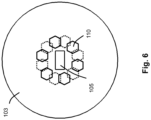
- Figures 3 , 4 and 5 illustrate examples with circular holes 110 and figure 6 illustrate an example with hexagonal shaped holes 110.
- the holes 110 may also be triangular, rectangular etc.
- the example number of holes 110 is 6.
- the at least two holes 110 are distributed in one row around the end opening 105.
- Figures 3-6 described above illustrates an example where the holes 110 are distributed in one row around the end opening 105.
- Figure 7 illustrates an example not covered by the claims where the holes 110 are distributed in two rows around the end opening 105.
- the inner row (the row being closest to the end opening 105) comprises 6 holes 110 and the outer row (the row being further away from the end opening 105 compared to the inner row) comprises 9 holes 110.
- two rows of holes 110 is only an example, and that a flange 103 may comprise any suitable number of rows of holes 110 and also number of holes 110.
- the holes 110 may be provided to each flange 103 using any suitable method such as drilling, moulding etc.
- Each flange 103 may have any suitable shape, for example a circular, rectangular, triangular, hexagonal etc.
- the flanges 103 on each waveguide 101 are preferably of the same shape.
- the flanges 103 may be a circular disk having at least two holes 110 on each flange 103.
- Each flange 103 may be of any suitable material such as metal, copper, aluminum, brass, gold, silver, metallized plastic or any other suitable material having sufficient electrical conductivity.
- the two waveguides 101 are arranged to be connected to each other by connecting e.g. the first flange 103a to the second flanges 103b such that the end openings 105a, 105b face each other and such that the holes 110 in the first flange 103a are at least partly glide symmetrically positioned with respect to the holes 110 in the second flange 103b.
- the connected first and second flanges 103a, 103b may then be described as mating flanges 103.
- the joined flanges 103 having at least two holes 110 that are periodically distributed around the opening may form an EBG structure.
- the embodiments herein use an at least partly glide symmetric periodic structure composed of for example a holey-unit cell as exemplified in figure 8 .
- a unit-cell may be described as a part of the structure, that when repeated periodically, builds up the complete waveguide 101.
- the unit cell can be one hole 110 in the first flange 103a plus two halves of two different holes 110 in the second flange 103b.
- the right part of figure 8 illustrates a graph (i.e.
- the x-axis of the graph represents the boundaries of a Brillouin zone and the y-axis of the graph represents the frequency measured in GHz.
- the X, M and gamma in the x-axis correspond to the points shown in the holey unit-cell at the left side of figure 8 (they are corners of a Brillouin zone).
- the stopband is between 40 and 77 GHz.
- the stopband is the band between the dotted lines in figure 8 .
- the solid lines in figure 8 represent propagating modes (i.e. different orientation of fields), the x-axis is different directions, and it is seen that there exists a frequency band (i.e. the stop band) where no modes can propagate in any direction. As seen, no wave can propagate inside the stopband.
- a stopband may be described as a band of frequencies, between specified limits, through which currents are not allowed to pass.
- Figure 9 is a graph illustrating the effect in the stopband for different gap size variations.
- the x-axis of figure 9 represents the gap 112 measured in ⁇ m and the y-axis represents the frequency measured in GHz.
- the previous example hole dimensions i.e. the ones seen in figure 8
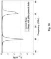
- Figure 10 is a graph illustrating a comparison of the transmission in a prior art flange having a smooth surface and a flange 103 with at least partly glide symmetric holes as in the embodiments herein in case of having a gap 112 of 0.05 mm between the first flange 103a and the second flange 103b.
- the x-axis of figure 10 represents the frequency measured in GHz and the y-axis represents transmission parameter (S 21 ) measured in dB.
- S 21 represents the power transmitted from one waveguide 101 to the other (i.e. not through the gap 112 between the flanges 103).
- the transmission in the prior art (normal) flange is illustrated with a dotted line and the transmission in the flange 103 with the at least partly glide symmetric holes 112 is illustrated with a continuous line.
- a first flange 103a surrounding an end opening 105a to the first waveguide 101a is provided.
- the first flange 103a comprises at least two holes 110 which are periodically distributed around the end opening 105a.
- the first waveguide 101a is arranged to be connected to a second waveguide 101b by connecting the first flange 103a to a second flange 103b of the second waveguide 101b such that the end opening 105a of the first waveguide 101a face an end opening 105b of the second waveguide 101b and such that the holes 110 in the first flange 103a are at least partly glide symmetrically positioned with respect to holes 110 which are periodically distributed around the end opening 105b of the second flange 103b.
- the at least two holes 110 comprised in the first flange 103a may constitute a holey and at least partly glide symmetric EBG structure integrated within the first flange 103a.
- the at least two holes 110 in the first flange 103a may be placed in a closed shape around the end opening 105a of the first flange 103a.
- the at least two holes 110 in the first flange 103a may be periodically distributed around the end opening 105a of the first flange 103a in at least one row.
- Each of the at least two holes 110 on the first flange 103a are at least one of circular, squared or hexagonal shaped.
- the at least two holes 110 on the first flange 103a are periodically distributed around the end opening 105a in a circular, a hexagonal or a polygonal form.
- the first flange 103a may be located around an outer circumference of the first waveguide 101a.
- the first waveguide 101a may be arranged to be connected to a second waveguide 101b such that a gap 112 of zero or more is located between the first flange 103a and the second flange 103b when they are connected.
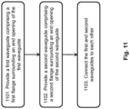
- the method for manufacturing a waveguide assembly for waveguides 101 will now be described with reference to the flowchart depicted in Figure 11 .
- the method comprises at least one of the following steps, which steps may as well be carried out in another suitable order than described below:
- a first waveguide 101a comprising a first flange 103a surrounding an end opening 105a of the first waveguide 101a is provided.
- a second waveguide 101b comprising a second flange 103b surrounding an end opening 105b of the second waveguide 101b is provided.
- Each flange 103a, 103b comprises at least two holes 110 which are periodically distributed around the respective end opening 105a, 105b.
- the first and second waveguides 101a, 101b are connected to each other by connecting the first flange 103a to the second flange 103b such that the end openings 105a, 105b face each other and such that the holes 110 in the first flange 103a are at least partly glide symmetrically positioned with respect to the holes 110 in the second flange 103b.
- the at least two holes 110 comprised in each flange 103a, 103b may constitutes a holey and at least partly glide symmetric EBG structure integrated within each of the first and second flanges 103a, 103b.
- the at least two holes 110 in each flange 103a, 103b are placed in a closed shape around the respective end opening 105a, 105b.
- the at least two holes 110 in each flange 103a, 103b may be periodically distributed around the respective end opening 105a, 105b in at least one row.
- the at least two holes 110 on each flange 103a, 103b may be at least one of: circular, squared or hexagonal shaped.
- the at least two holes 110 on each flange 103a, 103b may be periodically distributed around each end opening 105a, 105b in a circular, a hexagonal or a polygonal form.
- the first flange 103a may be located around an outer circumference of the first waveguide 101a and the second flange 103b may be located around an outer circumference of the second waveguide 101b.
- a gap 112 of zero or more may be located between the first flange 103a and the second flange 103b when they are connected.
- the flange 103 may be referred to as a holey and at least partly glide symmetric flange 103.
- the holey at least partly glide symmetric flange 103 is placed surrounding the waveguide end opening 105 and significantly reduces the leakage, should there be a gap 112 between the mated flanges 103.
- This waveguide 101 is easier to manufacture than the pin surface applied in the pin-flange since it just requires drilling holes which is much faster and easier than milling, casting, moulding or die-sinking pins.
Landscapes
- Physics & Mathematics (AREA)
- Electromagnetism (AREA)
- Optics & Photonics (AREA)
- Engineering & Computer Science (AREA)
- Manufacturing & Machinery (AREA)
- Waveguides (AREA)
- Waveguide Connection Structure (AREA)
Claims (8)
- Wellenleiteranordnung für Wellenleiter (101a, 101b), wobei die Wellenleiteranordnung umfasst:einen ersten Wellenleiter (101a), umfassend einen ersten Flansch (103a), der eine Endöffnung (105a) des ersten Wellenleiters (101a) umgibt;einen zweiten Wellenleiter (101b), umfassend einen zweiten Flansch (103b), der eine Endöffnung (105b) des zweiten Wellenleiters (101b) umgibt;wobei jeder Flansch (103a, 103b) mindestens zwei Löcher (110) umfasst, die periodisch um die jeweilige Endöffnung (105a, 105b) verteilt sind; und wobei der erste und zweite Wellenleiter (101a, 101b) angeordnet sind, um miteinander durch Verbinden des ersten Flansches (103a) mit dem zweiten Flansch (103b) verbunden zu werden, sodass die Endöffnungen (105a, 105b) zueinander zeigen, und sodass die Löcher (110) in dem ersten Flansch (103a) in Bezug auf die Löcher (110) in dem zweiten Flansch (103b) mindestens teilweise gleitsymmetrisch positioniert sind,wobei sich die mindestens zwei Löcher (110) in dem ersten Flansch (103a) mindestens teilweise mit den mindestens zwei Löchern (110) in dem zweiten Flansch (103b) überschneiden, sodass die Löcher (110) in dem ersten Flansch (103) in Bezug auf die mindestens zwei Löcher (110) in dem zweiten Flansch (103) über eine bestimmte Periode geglitten werden, wenn der erste und zweite Flansch (103a, 103b) verbunden sind,wobei die mindestens teilweise gleitsymmetrischen Löcher (110) konfiguriert sind, um Leckage von Signalen zu verhindern, die durch den ersten und zweiten Wellenleiter (101a, 101b) an der Verbindungsstelle zwischen dem ersten und zweiten Flansch (103a, 103b) geleitet werden, wobei alle der mindestens zwei Löcher (110) in jedem Flansch (103a, 103b) periodisch um die jeweilige Endöffnung (105a, 105b) in einer Reihe verteilt sind,wobei die mindestens teilweise gleitsymmetrisch positionierte vollkommen gleitsymmetrisch positionierte oder quasi gleitsymmetrisch positionierte umfasst, undwobei die quasi gleitsymmetrisch positionierte eine geringe Abweichung von einer exakt gleitsymmetrischen Struktur umfasst.
- Wellenleiteranordnung nach Anspruch 1, wobei die mindestens zwei Löcher (110), die in jedem Flansch (103a, 103b) enthalten sind, eine löchrige und mindestens teilweise gleitsymmetrische elektromagnetische Bandabstand-, EBG-Struktur darstellt, die innerhalb von jedem von dem ersten und zweiten Flansch (103a, 103b) integriert ist.
- Wellenleiteranordnung nach einem der Ansprüche 1-2, wobei die mindestens zwei Löcher (110) in jedem Flansch (103a, 103b) in einer geschlossenen Form um die jeweilige Endöffnung (105a, 105b) herum platziert sind.
- Wellenleiteranordnung nach einem der Ansprüche 1-3, wobei sich der erste Flansch (103a) um einen Außenumfang des ersten Wellenleiters (101a) befindet, und sich der zweite Flansch (103b) um einen Außenumfang des zweiten Wellenleiters (101b) befindet.
- Wellenleiteranordnung nach einem der Ansprüche 1-4, wobei sich ein Spalt (112) mit einer Länge gleich oder größer null zwischen dem ersten Flansch (103a) und dem zweiten Flansch (103b) befindet, wenn sie verbunden sind.
- Wellenleiteranordnung nach einem der Ansprüche 1-5, wobei die mindestens zwei Löcher (110) an jedem Flansch (103a, 103b) mindestens eines sind von: kreisförmig, quadratisch oder sechseckig geformt.
- Wellenleiteranordnung nach einem der Ansprüche 1-6, wobei die mindestens zwei Löcher (110) an jedem Flansch (103a, 103b) periodisch um jede Endöffnung (105a, 105b) in einer kreisförmigen, einer sechseckigen oder einer polygonalen Form verteilt sind.
- Verfahren zum Herstellen einer Wellenleiteranordnung für Wellenleiter (101a, 101b), wobei das Verfahren umfasst:Bereitstellen (110) eines ersten Wellenleiters (101a), umfassend einen ersten Flansch (103a), der eine Endöffnung (105a) des ersten Wellenleiters (101a) umgibt;Bereitstellen (1102) eines zweiten Wellenleiters (101b), umfassend einen zweiten Flansch (103b), der eine Endöffnung (105b) des zweiten Wellenleiters (101b) umgibt; wobei jeder Flansch (103a, 103b) mindestens zwei Löcher (110) umfasst, die periodisch um die jeweilige Endöffnung (105a, 105b) verteilt sind; undVerbinden (1103) des ersten und zweiten Wellenleiters (101a, 101b) miteinander durch Verbinden des ersten Flansches (103a) mit dem zweiten Flansch (103b), sodass die Endöffnungen (105a, 105b) zueinander zeigen und sodass die Löcher (110) in dem ersten Flansch (103a) in Bezug auf die Löcher (110) im zweiten Flansch (103b) mindestens teilweise gleitsymmetrisch positioniert sind,wobei sich die mindestens zwei Löcher (110) in dem ersten Flansch (103a) mindestens teilweise mit den mindestens zwei Löchern (110) in dem zweiten Flansch (103b) überschneiden, sodass die Löcher (110) in dem ersten Flansch (103) in Bezug auf die mindestens zwei Löcher (110) in dem zweiten Flansch (103) über eine bestimmte Periode geglitten werden, wenn der erste und zweite Flansch (103a, 103b) verbunden sind,wobei die mindestens teilweise gleitsymmetrischen Löcher (110) konfiguriert sind, um Leckage von Signalen zu verhindern, die durch den ersten und zweiten Wellenleiter (101a, 101b) an der Verbindungsstelle zwischen dem ersten und zweiten Flansch (103a, 103b) geleitet werden, wobei alle der mindestens zwei Löcher (110) in jedem Flansch (103a, 103b) periodisch um die jeweilige Endöffnung (105a, 105b) in einer Reihe verteilt sind,wobei die mindestens teilweise gleitsymmetrisch positionierte vollkommen gleitsymmetrisch positionierte oder quasi gleitsymmetrisch positionierte umfasst, undwobei die quasi gleitsymmetrisch positionierte eine geringe Abweichung von einer exakt gleitsymmetrischen Struktur umfasst.
Applications Claiming Priority (1)
| Application Number | Priority Date | Filing Date | Title |
|---|---|---|---|
| PCT/EP2017/076187 WO2019072399A1 (en) | 2017-10-13 | 2017-10-13 | SYMMETRICALLY SLIDED POSITIONED HOLES GUIDE INTERCONNECTION FOR AVOIDING A LEAK |
Publications (2)
| Publication Number | Publication Date |
|---|---|
| EP3695455A1 EP3695455A1 (de) | 2020-08-19 |
| EP3695455B1 true EP3695455B1 (de) | 2023-07-12 |
Family
ID=60117673
Family Applications (1)
| Application Number | Title | Priority Date | Filing Date |
|---|---|---|---|
| EP17784629.2A Active EP3695455B1 (de) | 2017-10-13 | 2017-10-13 | Wellenleiterverbindung mit gleitsymmetrisch positionierten löchern zur vermeidung von leckage |
Country Status (3)
| Country | Link |
|---|---|
| US (1) | US11387529B2 (de) |
| EP (1) | EP3695455B1 (de) |
| WO (1) | WO2019072399A1 (de) |
Families Citing this family (8)
| Publication number | Priority date | Publication date | Assignee | Title |
|---|---|---|---|---|
| SE541861C2 (en) | 2017-10-27 | 2019-12-27 | Metasum Ab | Multi-layer waveguide, arrangement, and method for production thereof |
| CN110600838A (zh) * | 2019-09-20 | 2019-12-20 | 盛纬伦(深圳)通信技术有限公司 | 一种防止电磁波信号泄露的波导接口结构 |
| CN110690535A (zh) * | 2019-10-09 | 2020-01-14 | 盛纬伦(深圳)通信技术有限公司 | 一种防止电磁波信号泄露的波导接口结构 |
| SE544108C2 (en) * | 2019-10-18 | 2021-12-28 | Metasum Ab | Multi-layer filter, arrangement, and method for production thereof |
| WO2022063441A1 (en) * | 2020-09-28 | 2022-03-31 | Telefonaktiebolaget Lm Ericsson (Publ) | Antenna assembly |
| CN118435064A (zh) * | 2021-12-22 | 2024-08-02 | 华为技术有限公司 | 微波天线探针 |
| JP2025050371A (ja) * | 2023-09-22 | 2025-04-04 | 株式会社Soken | 導波管 |
| CN121394824A (zh) * | 2024-07-23 | 2026-01-23 | 中兴通讯股份有限公司 | 波导连接结构及微波系统 |
Citations (1)
| Publication number | Priority date | Publication date | Assignee | Title |
|---|---|---|---|---|
| US20130342288A1 (en) * | 2012-06-21 | 2013-12-26 | Oml, Inc. | Self Keying and Orientation System for a Repeatable Waveguide Calibration and Connection |
Family Cites Families (5)
| Publication number | Priority date | Publication date | Assignee | Title |
|---|---|---|---|---|
| US3201725A (en) * | 1962-12-17 | 1965-08-17 | Varian Associates | Coupling means |
| US7791438B2 (en) * | 2007-06-07 | 2010-09-07 | Oml, Inc. | Millimeter and sub-millimeter wave waveguide interface having a junction of tight tolerance and a junction of lesser tolerance |
| US8693828B2 (en) * | 2010-05-11 | 2014-04-08 | The United States Of America As Represented By The Administrator Of The National Aeronautics Space Administration | Photonic choke-joints for dual polarization waveguides |
| WO2014174494A2 (en) * | 2013-04-26 | 2014-10-30 | Swissto12 Sa | Flanges for connection between corrugated wave-guiding modules |
| WO2018137997A1 (en) * | 2017-01-24 | 2018-08-02 | Huber+Suhner Ag | Waveguide assembly |
-
2017
- 2017-10-13 EP EP17784629.2A patent/EP3695455B1/de active Active
- 2017-10-13 WO PCT/EP2017/076187 patent/WO2019072399A1/en not_active Ceased
- 2017-10-13 US US16/647,891 patent/US11387529B2/en active Active
Patent Citations (1)
| Publication number | Priority date | Publication date | Assignee | Title |
|---|---|---|---|---|
| US20130342288A1 (en) * | 2012-06-21 | 2013-12-26 | Oml, Inc. | Self Keying and Orientation System for a Repeatable Waveguide Calibration and Connection |
Also Published As
| Publication number | Publication date |
|---|---|
| US11387529B2 (en) | 2022-07-12 |
| EP3695455A1 (de) | 2020-08-19 |
| WO2019072399A1 (en) | 2019-04-18 |
| WO2019072399A8 (en) | 2020-05-22 |
| US20200220245A1 (en) | 2020-07-09 |
Similar Documents
| Publication | Publication Date | Title |
|---|---|---|
| US11387529B2 (en) | Waveguides interconnected by flanges having glide symmetrically positioned holes disposed therein | |
| Ebrahimpouri et al. | Using glide-symmetric holes to reduce leakage between waveguide flanges | |
| US12249747B2 (en) | Non-contacting waveguide flange adapter element having quasi-periodic protruding elements configured to pass waves in one direction and stop waves in other directions | |
| US7791438B2 (en) | Millimeter and sub-millimeter wave waveguide interface having a junction of tight tolerance and a junction of lesser tolerance | |
| US11289787B2 (en) | Transition arrangement comprising a waveguide twist, a waveguide structure comprising a number of waveguide twists and a rotary joint | |
| Henke et al. | Minimizing RF performance spikes in a cryogenic orthomode transducer (OMT) | |
| CN104900956A (zh) | 一种波导到基片集成波导的转换装置 | |
| EP2116820B1 (de) | Verwendung einer Anpassvorrichtung, Messgerät mit Anpassvorrichtung und Verfahren zum Betreiben eines Wellenleiters | |
| US8693828B2 (en) | Photonic choke-joints for dual polarization waveguides | |
| Matthaei et al. | Novel staggered resonator array superconducting 2.3-GHz bandpass filter | |
| US7439831B2 (en) | Transition circuit | |
| JPS61216501A (ja) | 超楕円導波管接続装置 | |
| Herran et al. | Electromagnetic bandgap based on a compact three-hole double-layer periodic structure | |
| Alfonso et al. | Contactless flange adapters for mm-wave measurements | |
| JP4575313B2 (ja) | 導波管接続部 | |
| Mayaka et al. | Robust contactless waveguide flange for fast measurements | |
| US12199691B2 (en) | Waveguide component for high frequency testing | |
| Cui et al. | A compact waveguide connection for space applications using gap waveguide technology | |
| US11804681B1 (en) | Waveguide to coaxial conductor pin connector | |
| CN114518476A (zh) | 信号测量电路装置 | |
| Chen et al. | Multi-layer 3-dB directional coupler based on corrugated substrate integrated waveguide | |
| CN217740761U (zh) | 波导同轴转换器 | |
| Sammoura et al. | Micromachined plastic W-band bandpass filters | |
| JP5462298B2 (ja) | 導波管接続構造 | |
| Zhao et al. | Design of A Terahertz Waveguide Bidirectional Coupler |
Legal Events
| Date | Code | Title | Description |
|---|---|---|---|
| STAA | Information on the status of an ep patent application or granted ep patent |
Free format text: STATUS: UNKNOWN |
|
| STAA | Information on the status of an ep patent application or granted ep patent |
Free format text: STATUS: THE INTERNATIONAL PUBLICATION HAS BEEN MADE |
|
| PUAI | Public reference made under article 153(3) epc to a published international application that has entered the european phase |
Free format text: ORIGINAL CODE: 0009012 |
|
| STAA | Information on the status of an ep patent application or granted ep patent |
Free format text: STATUS: REQUEST FOR EXAMINATION WAS MADE |
|
| 17P | Request for examination filed |
Effective date: 20200409 |
|
| AK | Designated contracting states |
Kind code of ref document: A1 Designated state(s): AL AT BE BG CH CY CZ DE DK EE ES FI FR GB GR HR HU IE IS IT LI LT LU LV MC MK MT NL NO PL PT RO RS SE SI SK SM TR |
|
| AX | Request for extension of the european patent |
Extension state: BA ME |
|
| RIN1 | Information on inventor provided before grant (corrected) |
Inventor name: EBRAHIMPOURI HAMLKAR, MAHSA Inventor name: QUEVEDO-TERUEL, OSCAR Inventor name: MANHOLM, LARS Inventor name: ALGABA BRAZALEZ, ASTRID |
|
| DAV | Request for validation of the european patent (deleted) | ||
| DAX | Request for extension of the european patent (deleted) | ||
| STAA | Information on the status of an ep patent application or granted ep patent |
Free format text: STATUS: EXAMINATION IS IN PROGRESS |
|
| 17Q | First examination report despatched |
Effective date: 20210721 |
|
| GRAP | Despatch of communication of intention to grant a patent |
Free format text: ORIGINAL CODE: EPIDOSNIGR1 |
|
| STAA | Information on the status of an ep patent application or granted ep patent |
Free format text: STATUS: GRANT OF PATENT IS INTENDED |
|
| INTG | Intention to grant announced |
Effective date: 20230210 |
|
| GRAS | Grant fee paid |
Free format text: ORIGINAL CODE: EPIDOSNIGR3 |
|
| GRAA | (expected) grant |
Free format text: ORIGINAL CODE: 0009210 |
|
| STAA | Information on the status of an ep patent application or granted ep patent |
Free format text: STATUS: THE PATENT HAS BEEN GRANTED |
|
| AK | Designated contracting states |
Kind code of ref document: B1 Designated state(s): AL AT BE BG CH CY CZ DE DK EE ES FI FR GB GR HR HU IE IS IT LI LT LU LV MC MK MT NL NO PL PT RO RS SE SI SK SM TR |
|
| REG | Reference to a national code |
Ref country code: CH Ref legal event code: EP |
|
| REG | Reference to a national code |
Ref country code: IE Ref legal event code: FG4D |
|
| REG | Reference to a national code |
Ref country code: DE Ref legal event code: R096 Ref document number: 602017071233 Country of ref document: DE |
|
| REG | Reference to a national code |
Ref country code: LT Ref legal event code: MG9D |
|
| REG | Reference to a national code |
Ref country code: NL Ref legal event code: MP Effective date: 20230712 |
|
| REG | Reference to a national code |
Ref country code: AT Ref legal event code: MK05 Ref document number: 1588097 Country of ref document: AT Kind code of ref document: T Effective date: 20230712 |
|
| PG25 | Lapsed in a contracting state [announced via postgrant information from national office to epo] |
Ref country code: NL Free format text: LAPSE BECAUSE OF FAILURE TO SUBMIT A TRANSLATION OF THE DESCRIPTION OR TO PAY THE FEE WITHIN THE PRESCRIBED TIME-LIMIT Effective date: 20230712 |
|
| PG25 | Lapsed in a contracting state [announced via postgrant information from national office to epo] |
Ref country code: GR Free format text: LAPSE BECAUSE OF FAILURE TO SUBMIT A TRANSLATION OF THE DESCRIPTION OR TO PAY THE FEE WITHIN THE PRESCRIBED TIME-LIMIT Effective date: 20231013 |
|
| PGFP | Annual fee paid to national office [announced via postgrant information from national office to epo] |
Ref country code: GB Payment date: 20231027 Year of fee payment: 7 |
|
| PG25 | Lapsed in a contracting state [announced via postgrant information from national office to epo] |
Ref country code: ES Free format text: LAPSE BECAUSE OF FAILURE TO SUBMIT A TRANSLATION OF THE DESCRIPTION OR TO PAY THE FEE WITHIN THE PRESCRIBED TIME-LIMIT Effective date: 20230712 |
|
| PG25 | Lapsed in a contracting state [announced via postgrant information from national office to epo] |
Ref country code: IS Free format text: LAPSE BECAUSE OF FAILURE TO SUBMIT A TRANSLATION OF THE DESCRIPTION OR TO PAY THE FEE WITHIN THE PRESCRIBED TIME-LIMIT Effective date: 20231112 |
|
| PG25 | Lapsed in a contracting state [announced via postgrant information from national office to epo] |
Ref country code: SE Free format text: LAPSE BECAUSE OF FAILURE TO SUBMIT A TRANSLATION OF THE DESCRIPTION OR TO PAY THE FEE WITHIN THE PRESCRIBED TIME-LIMIT Effective date: 20230712 Ref country code: RS Free format text: LAPSE BECAUSE OF FAILURE TO SUBMIT A TRANSLATION OF THE DESCRIPTION OR TO PAY THE FEE WITHIN THE PRESCRIBED TIME-LIMIT Effective date: 20230712 Ref country code: PT Free format text: LAPSE BECAUSE OF FAILURE TO SUBMIT A TRANSLATION OF THE DESCRIPTION OR TO PAY THE FEE WITHIN THE PRESCRIBED TIME-LIMIT Effective date: 20231113 Ref country code: NO Free format text: LAPSE BECAUSE OF FAILURE TO SUBMIT A TRANSLATION OF THE DESCRIPTION OR TO PAY THE FEE WITHIN THE PRESCRIBED TIME-LIMIT Effective date: 20231012 Ref country code: LV Free format text: LAPSE BECAUSE OF FAILURE TO SUBMIT A TRANSLATION OF THE DESCRIPTION OR TO PAY THE FEE WITHIN THE PRESCRIBED TIME-LIMIT Effective date: 20230712 Ref country code: LT Free format text: LAPSE BECAUSE OF FAILURE TO SUBMIT A TRANSLATION OF THE DESCRIPTION OR TO PAY THE FEE WITHIN THE PRESCRIBED TIME-LIMIT Effective date: 20230712 Ref country code: IS Free format text: LAPSE BECAUSE OF FAILURE TO SUBMIT A TRANSLATION OF THE DESCRIPTION OR TO PAY THE FEE WITHIN THE PRESCRIBED TIME-LIMIT Effective date: 20231112 Ref country code: HR Free format text: LAPSE BECAUSE OF FAILURE TO SUBMIT A TRANSLATION OF THE DESCRIPTION OR TO PAY THE FEE WITHIN THE PRESCRIBED TIME-LIMIT Effective date: 20230712 Ref country code: GR Free format text: LAPSE BECAUSE OF FAILURE TO SUBMIT A TRANSLATION OF THE DESCRIPTION OR TO PAY THE FEE WITHIN THE PRESCRIBED TIME-LIMIT Effective date: 20231013 Ref country code: FI Free format text: LAPSE BECAUSE OF FAILURE TO SUBMIT A TRANSLATION OF THE DESCRIPTION OR TO PAY THE FEE WITHIN THE PRESCRIBED TIME-LIMIT Effective date: 20230712 Ref country code: ES Free format text: LAPSE BECAUSE OF FAILURE TO SUBMIT A TRANSLATION OF THE DESCRIPTION OR TO PAY THE FEE WITHIN THE PRESCRIBED TIME-LIMIT Effective date: 20230712 Ref country code: AT Free format text: LAPSE BECAUSE OF FAILURE TO SUBMIT A TRANSLATION OF THE DESCRIPTION OR TO PAY THE FEE WITHIN THE PRESCRIBED TIME-LIMIT Effective date: 20230712 |
|
| PG25 | Lapsed in a contracting state [announced via postgrant information from national office to epo] |
Ref country code: PL Free format text: LAPSE BECAUSE OF FAILURE TO SUBMIT A TRANSLATION OF THE DESCRIPTION OR TO PAY THE FEE WITHIN THE PRESCRIBED TIME-LIMIT Effective date: 20230712 |
|
| REG | Reference to a national code |
Ref country code: DE Ref legal event code: R097 Ref document number: 602017071233 Country of ref document: DE |
|
| PG25 | Lapsed in a contracting state [announced via postgrant information from national office to epo] |
Ref country code: SM Free format text: LAPSE BECAUSE OF FAILURE TO SUBMIT A TRANSLATION OF THE DESCRIPTION OR TO PAY THE FEE WITHIN THE PRESCRIBED TIME-LIMIT Effective date: 20230712 Ref country code: RO Free format text: LAPSE BECAUSE OF FAILURE TO SUBMIT A TRANSLATION OF THE DESCRIPTION OR TO PAY THE FEE WITHIN THE PRESCRIBED TIME-LIMIT Effective date: 20230712 Ref country code: EE Free format text: LAPSE BECAUSE OF FAILURE TO SUBMIT A TRANSLATION OF THE DESCRIPTION OR TO PAY THE FEE WITHIN THE PRESCRIBED TIME-LIMIT Effective date: 20230712 Ref country code: DK Free format text: LAPSE BECAUSE OF FAILURE TO SUBMIT A TRANSLATION OF THE DESCRIPTION OR TO PAY THE FEE WITHIN THE PRESCRIBED TIME-LIMIT Effective date: 20230712 Ref country code: CZ Free format text: LAPSE BECAUSE OF FAILURE TO SUBMIT A TRANSLATION OF THE DESCRIPTION OR TO PAY THE FEE WITHIN THE PRESCRIBED TIME-LIMIT Effective date: 20230712 Ref country code: SK Free format text: LAPSE BECAUSE OF FAILURE TO SUBMIT A TRANSLATION OF THE DESCRIPTION OR TO PAY THE FEE WITHIN THE PRESCRIBED TIME-LIMIT Effective date: 20230712 |
|
| REG | Reference to a national code |
Ref country code: DE Ref legal event code: R119 Ref document number: 602017071233 Country of ref document: DE |
|
| PLBE | No opposition filed within time limit |
Free format text: ORIGINAL CODE: 0009261 |
|
| STAA | Information on the status of an ep patent application or granted ep patent |
Free format text: STATUS: NO OPPOSITION FILED WITHIN TIME LIMIT |
|
| PG25 | Lapsed in a contracting state [announced via postgrant information from national office to epo] |
Ref country code: IT Free format text: LAPSE BECAUSE OF FAILURE TO SUBMIT A TRANSLATION OF THE DESCRIPTION OR TO PAY THE FEE WITHIN THE PRESCRIBED TIME-LIMIT Effective date: 20230712 Ref country code: MC Free format text: LAPSE BECAUSE OF FAILURE TO SUBMIT A TRANSLATION OF THE DESCRIPTION OR TO PAY THE FEE WITHIN THE PRESCRIBED TIME-LIMIT Effective date: 20230712 |
|
| REG | Reference to a national code |
Ref country code: CH Ref legal event code: PL |
|
| REG | Reference to a national code |
Ref country code: BE Ref legal event code: MM Effective date: 20231031 |
|
| 26N | No opposition filed |
Effective date: 20240415 |
|
| PG25 | Lapsed in a contracting state [announced via postgrant information from national office to epo] |
Ref country code: LU Free format text: LAPSE BECAUSE OF NON-PAYMENT OF DUE FEES Effective date: 20231013 |
|
| PG25 | Lapsed in a contracting state [announced via postgrant information from national office to epo] |
Ref country code: LU Free format text: LAPSE BECAUSE OF NON-PAYMENT OF DUE FEES Effective date: 20231013 |
|
| PG25 | Lapsed in a contracting state [announced via postgrant information from national office to epo] |
Ref country code: CH Free format text: LAPSE BECAUSE OF NON-PAYMENT OF DUE FEES Effective date: 20231031 |
|
| PG25 | Lapsed in a contracting state [announced via postgrant information from national office to epo] |
Ref country code: FR Free format text: LAPSE BECAUSE OF NON-PAYMENT OF DUE FEES Effective date: 20231031 Ref country code: DE Free format text: LAPSE BECAUSE OF NON-PAYMENT OF DUE FEES Effective date: 20240501 Ref country code: CH Free format text: LAPSE BECAUSE OF NON-PAYMENT OF DUE FEES Effective date: 20231031 Ref country code: SI Free format text: LAPSE BECAUSE OF FAILURE TO SUBMIT A TRANSLATION OF THE DESCRIPTION OR TO PAY THE FEE WITHIN THE PRESCRIBED TIME-LIMIT Effective date: 20230712 |
|
| PG25 | Lapsed in a contracting state [announced via postgrant information from national office to epo] |
Ref country code: BE Free format text: LAPSE BECAUSE OF NON-PAYMENT OF DUE FEES Effective date: 20231031 |
|
| PG25 | Lapsed in a contracting state [announced via postgrant information from national office to epo] |
Ref country code: IE Free format text: LAPSE BECAUSE OF NON-PAYMENT OF DUE FEES Effective date: 20231013 |
|
| PG25 | Lapsed in a contracting state [announced via postgrant information from national office to epo] |
Ref country code: IE Free format text: LAPSE BECAUSE OF NON-PAYMENT OF DUE FEES Effective date: 20231013 |
|
| PG25 | Lapsed in a contracting state [announced via postgrant information from national office to epo] |
Ref country code: BG Free format text: LAPSE BECAUSE OF FAILURE TO SUBMIT A TRANSLATION OF THE DESCRIPTION OR TO PAY THE FEE WITHIN THE PRESCRIBED TIME-LIMIT Effective date: 20230712 |
|
| PG25 | Lapsed in a contracting state [announced via postgrant information from national office to epo] |
Ref country code: BG Free format text: LAPSE BECAUSE OF FAILURE TO SUBMIT A TRANSLATION OF THE DESCRIPTION OR TO PAY THE FEE WITHIN THE PRESCRIBED TIME-LIMIT Effective date: 20230712 |
|
| GBPC | Gb: european patent ceased through non-payment of renewal fee |
Effective date: 20241013 |
|
| PG25 | Lapsed in a contracting state [announced via postgrant information from national office to epo] |
Ref country code: GB Free format text: LAPSE BECAUSE OF NON-PAYMENT OF DUE FEES Effective date: 20241013 |
|
| PG25 | Lapsed in a contracting state [announced via postgrant information from national office to epo] |
Ref country code: CY Free format text: LAPSE BECAUSE OF FAILURE TO SUBMIT A TRANSLATION OF THE DESCRIPTION OR TO PAY THE FEE WITHIN THE PRESCRIBED TIME-LIMIT; INVALID AB INITIO Effective date: 20171013 |
|
| PG25 | Lapsed in a contracting state [announced via postgrant information from national office to epo] |
Ref country code: HU Free format text: LAPSE BECAUSE OF FAILURE TO SUBMIT A TRANSLATION OF THE DESCRIPTION OR TO PAY THE FEE WITHIN THE PRESCRIBED TIME-LIMIT; INVALID AB INITIO Effective date: 20171013 |
|
| PG25 | Lapsed in a contracting state [announced via postgrant information from national office to epo] |
Ref country code: TR Free format text: LAPSE BECAUSE OF FAILURE TO SUBMIT A TRANSLATION OF THE DESCRIPTION OR TO PAY THE FEE WITHIN THE PRESCRIBED TIME-LIMIT Effective date: 20230712 |