EP3694207A1 - Dispositifs d'imagerie à ouvertures multiples 3d, dispositif d'imagerie à ouvertures multiples, procédé de fourniture d'un signal de sortie d'un dispositif d'imagerie à ouvertures multiples 3d et procédé de détection d'un champ visuel complet - Google Patents
Dispositifs d'imagerie à ouvertures multiples 3d, dispositif d'imagerie à ouvertures multiples, procédé de fourniture d'un signal de sortie d'un dispositif d'imagerie à ouvertures multiples 3d et procédé de détection d'un champ visuel complet Download PDFInfo
- Publication number
- EP3694207A1 EP3694207A1 EP20167218.5A EP20167218A EP3694207A1 EP 3694207 A1 EP3694207 A1 EP 3694207A1 EP 20167218 A EP20167218 A EP 20167218A EP 3694207 A1 EP3694207 A1 EP 3694207A1
- Authority
- EP
- European Patent Office
- Prior art keywords
- image sensor
- view
- aperture imaging
- imaging device
- sub
- Prior art date
- Legal status (The legal status is an assumption and is not a legal conclusion. Google has not performed a legal analysis and makes no representation as to the accuracy of the status listed.)
- Granted
Links
- 238000003384 imaging method Methods 0.000 title claims abstract description 331
- 238000000034 method Methods 0.000 title claims description 44
- 230000003287 optical effect Effects 0.000 claims abstract description 389
- 238000013507 mapping Methods 0.000 claims abstract description 19
- 238000012545 processing Methods 0.000 claims description 14
- 230000011218 segmentation Effects 0.000 claims description 14
- 230000002950 deficient Effects 0.000 claims description 5
- 230000000007 visual effect Effects 0.000 abstract description 14
- 239000000758 substrate Substances 0.000 description 61
- 230000006641 stabilisation Effects 0.000 description 27
- 238000011105 stabilization Methods 0.000 description 27
- 230000008859 change Effects 0.000 description 25
- 238000013461 design Methods 0.000 description 15
- 230000000694 effects Effects 0.000 description 14
- 239000000463 material Substances 0.000 description 14
- 238000004519 manufacturing process Methods 0.000 description 12
- 238000004590 computer program Methods 0.000 description 9
- 230000008569 process Effects 0.000 description 8
- 230000008901 benefit Effects 0.000 description 7
- 238000012937 correction Methods 0.000 description 7
- 230000006870 function Effects 0.000 description 7
- 238000009434 installation Methods 0.000 description 7
- 230000007246 mechanism Effects 0.000 description 7
- 238000003491 array Methods 0.000 description 5
- 230000001419 dependent effect Effects 0.000 description 5
- 238000006073 displacement reaction Methods 0.000 description 5
- 239000011521 glass Substances 0.000 description 5
- 229920000642 polymer Polymers 0.000 description 5
- 230000005855 radiation Effects 0.000 description 5
- 238000003860 storage Methods 0.000 description 5
- 238000004422 calculation algorithm Methods 0.000 description 4
- 238000011156 evaluation Methods 0.000 description 4
- 238000000465 moulding Methods 0.000 description 4
- 230000005540 biological transmission Effects 0.000 description 3
- 238000004364 calculation method Methods 0.000 description 3
- 238000010276 construction Methods 0.000 description 3
- 239000006059 cover glass Substances 0.000 description 3
- 238000009826 distribution Methods 0.000 description 3
- 238000005286 illumination Methods 0.000 description 3
- 238000005304 joining Methods 0.000 description 3
- 239000000203 mixture Substances 0.000 description 3
- 239000007787 solid Substances 0.000 description 3
- 239000000725 suspension Substances 0.000 description 3
- 238000010521 absorption reaction Methods 0.000 description 2
- 239000000969 carrier Substances 0.000 description 2
- 230000001427 coherent effect Effects 0.000 description 2
- 238000001514 detection method Methods 0.000 description 2
- 238000010586 diagram Methods 0.000 description 2
- 230000007613 environmental effect Effects 0.000 description 2
- 238000001746 injection moulding Methods 0.000 description 2
- 239000002245 particle Substances 0.000 description 2
- 238000001454 recorded image Methods 0.000 description 2
- 230000009467 reduction Effects 0.000 description 2
- 230000004044 response Effects 0.000 description 2
- 238000012546 transfer Methods 0.000 description 2
- 238000013519 translation Methods 0.000 description 2
- 239000012780 transparent material Substances 0.000 description 2
- 241001136792 Alle Species 0.000 description 1
- 229910000831 Steel Inorganic materials 0.000 description 1
- 230000001133 acceleration Effects 0.000 description 1
- 230000009471 action Effects 0.000 description 1
- 238000004026 adhesive bonding Methods 0.000 description 1
- 238000004458 analytical method Methods 0.000 description 1
- 230000009286 beneficial effect Effects 0.000 description 1
- 238000006243 chemical reaction Methods 0.000 description 1
- 238000005352 clarification Methods 0.000 description 1
- 238000004891 communication Methods 0.000 description 1
- 230000000295 complement effect Effects 0.000 description 1
- 230000006835 compression Effects 0.000 description 1
- 238000007906 compression Methods 0.000 description 1
- 238000011109 contamination Methods 0.000 description 1
- 230000007423 decrease Effects 0.000 description 1
- 239000006185 dispersion Substances 0.000 description 1
- 230000005520 electrodynamics Effects 0.000 description 1
- 230000001815 facial effect Effects 0.000 description 1
- 230000004927 fusion Effects 0.000 description 1
- 239000004973 liquid crystal related substance Substances 0.000 description 1
- 239000011159 matrix material Substances 0.000 description 1
- 238000005259 measurement Methods 0.000 description 1
- 239000007769 metal material Substances 0.000 description 1
- 229910044991 metal oxide Inorganic materials 0.000 description 1
- 150000004706 metal oxides Chemical class 0.000 description 1
- 238000012986 modification Methods 0.000 description 1
- 230000004048 modification Effects 0.000 description 1
- 238000012634 optical imaging Methods 0.000 description 1
- 230000002093 peripheral effect Effects 0.000 description 1
- 238000003825 pressing Methods 0.000 description 1
- 230000003014 reinforcing effect Effects 0.000 description 1
- 239000004065 semiconductor Substances 0.000 description 1
- 238000000926 separation method Methods 0.000 description 1
- 239000000243 solution Substances 0.000 description 1
- 230000003595 spectral effect Effects 0.000 description 1
- 238000001228 spectrum Methods 0.000 description 1
- 239000003381 stabilizer Substances 0.000 description 1
- 239000010959 steel Substances 0.000 description 1
- 230000007704 transition Effects 0.000 description 1
Images


Classifications
-
- H—ELECTRICITY
- H04—ELECTRIC COMMUNICATION TECHNIQUE
- H04N—PICTORIAL COMMUNICATION, e.g. TELEVISION
- H04N13/00—Stereoscopic video systems; Multi-view video systems; Details thereof
- H04N13/20—Image signal generators
- H04N13/204—Image signal generators using stereoscopic image cameras
- H04N13/239—Image signal generators using stereoscopic image cameras using two 2D image sensors having a relative position equal to or related to the interocular distance
-
- H—ELECTRICITY
- H04—ELECTRIC COMMUNICATION TECHNIQUE
- H04N—PICTORIAL COMMUNICATION, e.g. TELEVISION
- H04N13/00—Stereoscopic video systems; Multi-view video systems; Details thereof
- H04N13/10—Processing, recording or transmission of stereoscopic or multi-view image signals
- H04N13/106—Processing image signals
- H04N13/172—Processing image signals image signals comprising non-image signal components, e.g. headers or format information
- H04N13/178—Metadata, e.g. disparity information
-
- H—ELECTRICITY
- H04—ELECTRIC COMMUNICATION TECHNIQUE
- H04N—PICTORIAL COMMUNICATION, e.g. TELEVISION
- H04N23/00—Cameras or camera modules comprising electronic image sensors; Control thereof
- H04N23/45—Cameras or camera modules comprising electronic image sensors; Control thereof for generating image signals from two or more image sensors being of different type or operating in different modes, e.g. with a CMOS sensor for moving images in combination with a charge-coupled device [CCD] for still images
Definitions
- the present invention relates to 3D multi-aperture imaging devices and thus to multi-aperture imaging devices which are designed to capture an overall field of view at least stereoscopically, to a method for providing an output signal of a 3D multi-aperture imaging device and to a method for detecting an overall field of view.
- a concept that enables image processing of image data acquired with 3D multi-aperture imaging devices and multi-aperture imaging devices would also be desirable.
- a first aspect of the present invention is based on the knowledge that the generation of an output signal of a 3D multi-aperture imaging device is carried out in such a way that image information from pixels of the 3D multi-aperture imaging device is suitably linked with meta information to form an output signal, so that subsequent processing of the image information and / or a change in the same is made possible independently of the 3D multi-aperture imaging device, and at the same time essential information relating to the structure of the 3D multi-aperture imaging device can be taken into account and / or used.
- the concept of the output signal can be applied to various types of 3-D multi-aperture imaging devices, even if the 3-D multi-aperture imaging devices differ in structure.
- a second aspect of the present invention is based on the knowledge that an orientation or position of mutually adjacent partial fields of view of an overall field of view can be varied or transformed compared to an orientation or arrangement of mutually adjacent optical channels of a multi-aperture imaging device in order to create a single-line array of optical channels on a device or to a system in which or in which the multi-aperture imaging device is installed, without having to accept a restriction with regard to the field of view to be recorded.
- a 3D multi-aperture imaging device comprises an image sensor having a plurality of image sensor areas, wherein each image sensor area comprises a plurality of pixels.
- the 3D multi-aperture imaging device comprises a first plurality of optical channels for imaging overlapping first partial fields of view of an overall field of view onto first image sensor areas of the image sensor.
- the 3-D multi-aperture imaging device comprises a second plurality of optical channels for imaging one another and second fields of view of the total field of view overlapping with the first partial fields of view onto two image sensor areas of the image sensor.
- the first and the second plurality of optical channels are arranged laterally offset from one another by a base distance.
- the 3-D multi-aperture imaging device includes a processor that is implemented is to receive image sensor data from the image sensor which has information about the first and second partial fields of view mapped onto the first and second plurality of image sensor areas, and which is designed to provide an output signal which has a data header and useful data.
- the data header has information relating to the structure of the 3D multi-aperture imaging device.
- the useful data have image information obtained from the pixels of the first image sensor area and the second image sensor area.
- the advantage of this exemplary embodiment is that the useful data can be processed subsequently by taking into account the information contained in the data header with regard to the structure of the 3D multi-aperture imaging device.
- the structure of the 3D multi-aperture imaging device does not have to be completely known, since corresponding information can be obtained from the output signal. Images from different 3D multi-aperture imaging devices can thus be processed and the differences can be taken from the output signal itself.
- an image signal comprises a data header that has information relating to the structure of a 3D multi-aperture imaging device, and useful data that includes image information obtained from pixels of first image sensor areas and second image sensor areas of the 3D multi-aperture imaging device, the image information of the first and second image sensor areas being one another each relate to a plurality of partial fields of view of an overall field of view.
- the advantage of this is that the structure and / or processability of the useful data can be represented by the data header, so that the image data can be displayed in different ways, i.e. H. 3D multi-aperture imaging devices having a different structure from one another can be described with the aid of output signals which have the same structure, which enables the useful data to be processed with consistently high quality.
- a device for processing an input signal which has the features of the output signal or image signal described above, comprises an input interface for receiving the input signal and a processor for processing the useful data, taking into account the information relating to the structure of the 3D multi-aperture imaging device for at least first image sensor information of a first partial field of view and a second partial field of view.
- the advantage of this exemplary embodiment is that the device can receive and process input signals from 3D multi-aperture imaging devices each having a different structure.
- a method for providing an output signal of a 3D multi-aperture imaging device comprises the following steps: providing an image sensor with a plurality of image sensor areas, wherein each image sensor area comprises a plurality of pixels; Providing a plurality of optical channels for mapping overlapping first partial fields of view of an overall field of view onto first image sensor areas of the image sensor; Providing a second plurality of optical channels for imaging each other and with the first partial fields of view overlapping second partial fields of view of the total field of view on second image sensor areas of the image sensor, wherein the first and the second plurality of optical channels are arranged so that they are laterally offset from one another by a basic distance ; Receiving image sensor data from the image sensor, the image sensor data including the information about the first and second partial fields of view imaged onto the first and second plurality of image sensor areas; and generating the output signal so that the output signal has a data header and useful data, so that the data header contains information relating to the structure of the 3D multi-aperture imaging
- a multi-aperture imaging device comprises an image sensor with a plurality of image sensor areas, wherein each image sensor area comprises a plurality of pixels.
- the multi-aperture imaging device comprises a plurality of optical channels for imaging overlapping partial fields of view of an overall field of view onto image sensor areas of the image sensor.
- the plurality of optical channels form a one-dimensional array that is arranged along a first direction, while the partial fields of view of the (total) field of view form a one-dimensional array that is arranged along a second direction perpendicular to the first direction.
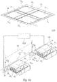
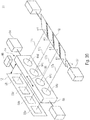
- Fig. 1a shows a schematic perspective view of a 3D Multiaperturab Struktursvorraum 1000.
- the 3D Multiaperturab Struktursvortechnik 1000 12 includes an image sensor, the image sensor 12 includes a plurality of image sensing areas 58 11-58 24th
- Each of the image sensor portions 58 11-58 24 includes a plurality of pixels so that each of the image sensor portions 58 11-58 24 is formed to a partial image to capture an overall image.
- the overall image can be understood as an image of an overall field of view 72.
- the 3D multi-aperture imaging device 1000 can have two or more modules 11 or multi-aperture imaging devices 11.
- Each of the multi-aperture imaging devices 11a and 11b can be designed to image the entire field of view at least almost completely or completely, and to form a channel of an at least stereoscopic detection system.
- a first channel can be, for example, a "right” channel, while a second channel can be a "left” channel.
- the designation left / right is not intended to have a restrictive effect in this context, but can also be designated using any other terms, such as top, bottom, center, front, back or the like.
- the 3D Multiaperturab For the detection of the 3D Multiaperturab Struktursvorraum 1000 includes, for example, a first module 11a having a first plurality of optical channels 16. 11 - 14, 16 which are arranged to form an array 14. 1 Further, the 3D Multiaperturab Struktursvortechnik 1000 includes a second module 11b having a second plurality of optical channels 16 21-16 24 which are arranged in a second array 14. 2 The modules 11a and 11b are with a Base spacing BA offset from one another so that at least stereoscopic information can be derived based on a disparity obtained thereby.
- Each of the optical channels 16 11 - 16 24 is designed to capture a partial field of view 74a - 74d or partial field of view 74a - 74d of an overall field of view 72.
- At least adjacent partial fields of view can overlap with one another, for example partial fields of view 74a and 74b or partial fields of view 74b and 74c, but also diagonally adjacent partial fields of view, such as partial fields of view 74a and 74c or 74b and 74d.
- the overlap can enable a simple calculation of the overall image from partial images in that the overlapping image areas provide information on how the partial images are to be put together, for example in the context of a stitching process.
- all sub-areas 74a-74d can also overlap one another.
- the optical channel 16 11 is designed, for example, to image the partial field of view 74a or 74 11 on the image sensor region 58 11 .
- the optical channel 16 21 is designed, for example, to image the partial field of view 74 a or 74 21 onto the image sensor region 58 21 .
- Each sub-area 74a-74d is thus mapped onto two image sensor areas by two optical channels.
- the partial area 74a is shown in such a way that it is mapped completely by the module 11a as partial field of view 74 11 and completely by the module 11b as partial field of view 74 21 , it is understood that the partial fields of view 74 11 and 74 21 are not completely identical are, for example, based on manufacturing tolerances. Such effects can, however, be compensated for by calibration or the like and are subsequently neglected.
- the image sensor portions 58 11-58 14 and the optical channels 16 11-16 14 may be components of the first imaging module 11a, while the image sensor portions 58 21-58 24 and the optical channels 16 21-16 24 components of the second imaging module 11b may be.
- Each of the imaging modules 11a and 11b is designed, for example, to capture the entire field of view 72, which means that the 3D multi-aperture imaging device can capture the entire field of view 72 stereoscopically by means of the modules 11a and 11b.
- the 3D Multiaperturab Struktursvorraum includes a processor 1002 that is configured to image sensor data 1004 11 - 1004 24 received from the second module 11b - 1004 14 of the first module 11a and the image sensor data 1004 21st
- the image sensor data 1004 11 - 1004 24 example, the signal or samples of the image sensor portions 58 11 - comprise or include values derived therefrom, such as a pixel value or a color value 58 24th
- the image sensor can be designed as a charge-coupled device (CCD), as a complementary metal oxide semiconductor (CMOS) or as a differently formed image sensor.
- CMOS complementary metal oxide semiconductor
- the image sensor data 1004 11 - 1004 24 may be the output values of the corresponding sensor or sensor part respectively. Regardless of the specific implementation, have the image sensor data 1004 11 - 1004 24 information on the image sensor portions 58 11-58 14 and 58 21-58 24 depicted partial fields 74 11-74 14 and 74, 21-74 24.
- the processor 1002 is designed to provide an output signal 1006 which has a data header 1008 and useful data 1012.
- the data header 1008 has information relating to the structure of the 3D multi-aperture imaging device 1000.
- the useful data 1012 have image information obtained from the pixels of the image sensor areas 58 11 - 58 14 and 58 21 - 58 24 . This may be the image sensor data 1004 11 - 1004 24 act or derived therefrom or processed information, which will be explained in detail later.
- the output signal 1006 can thus be an image signal. Alternatively, it can also be a video signal if several images of the entire field of view are recorded as video.
- the 3D multi-aperture imaging device 1000 can optionally have an output interface 1014, via which the output signal 1004 can be output.
- the output interface 1014 can be a wireless or wired interface.
- USB Universal Serial Bus
- the output interface 1014 can be designed to be wired or wireless Connect to another device, such as a computer or laptop.
- a memory module can also be arranged.
- modules 11a and 11b are shown so that the optical channels 16 11 and 16 21 the partial field of view 74a, the optical channels 16 12 and 16 22 the partial field of view 74b, the optical channels 16 13 and 16 23 the partial field of view 74c and the optical channels 16 14 and 16 24 capture the partial field of view 74d and are arranged in the modules 11a and 11b in the same order along a line extension direction 146 of the arrays 14 1 and 14 2 , the modules 11a and 11b can also be arranged in a different order and / or a have different numbers from each other.
- optical channel 16 21 can capture a partial field of view 74a-74d that is different from the optical channel 16 11
- the optical channel 16 22 can capture a partial field of view 74a-74d that is different from the optical channel 16 12
- the optical channel 16 23 can capture a partial field of view different from the optical channel 16 13 and / or that the optical channel 16 24 can capture a partial field of view 74a-74d different from the optical channel 16 14 .
- the partial fields of view 74a-74d can be mapped in such a way that there is an equal, constant disparity between optical channels which are directed to the same partial field of view 74a-74d, as shown in FIG Fig. 1a is described, or that alternatively different disparities can exist for different partial fields of view 74a-74d.
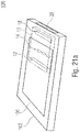
- Figure 1b shows the 3D multi-aperture imaging device 1000 as it can be used in accordance with the exemplary embodiments described here.
- the image sensor 12 can be divided into two components 12 1 and 12 2 , one component 12 1 for the “right” optical channels 16 1 and the other component 12 2 for the “left” channels 16 2 .
- This means that the image sensor 12 is off Fig. 1a several components can also be formed, with each module 11a and 11b, for example, being able to have one of the components.
- the right and left optical channels 16 1 and 16 2 are in the example of FIG Figure 1b Identically constructed, but arranged laterally offset from one another by the base distance BA in order to obtain as much depth information as possible with respect to the scene located in the field of view of the device 1000.
- each plurality 16 1 and 16 2 of optical channels comprises four optical channels arranged next to one another.
- the individual "right" channels are distinguished by the second subscript.
- the channels are indexed from right to left. That is, the optical channel 16 11 shown in Figure 1b is not shown because of a partial removal chosen for the sake of clarity, is arranged at the rightmost edge, ie farthest away from the majority, for example along the base spacing direction 108 along which the left and right channels are offset from one another at the base spacing BA 16 2 left channels, with the other right channels 16 12 - 16 14 following along the base spacing direction 108.
- the channels 16 11-16 14 thus form a single-line array of optical channels, the rows extending direction corresponds to the basic distance direction 108th
- the left channels 16 2 are also constructed. They too are distinguished from one another by the second subscript.
- the left channels 16 21 - 16 24 are arranged next to one another and in the same direction one after the other as the right channels 16 11 - 16 14 , namely in such a way that the channel 16 21 is closest to the right channels and the channel 16 24 is farthest away from The latter.
- the channel 16 11 maps the partial field of view 74 11 onto an image sensor area 58 11
- the optical channel 16 12 maps the partial field of view 74 12 onto an image sensor area 58 12
- the optical channel 16 13 maps an assigned partial field of view 74 13 onto a corresponding in Figure 1b non-visible image sensor area 58 13 of the image sensor 12 and the optical channel 16 14 an assigned partial field of view 74 14 to a corresponding image sensor area 58 14 , which is also shown in FIG Figure 1b is not shown due to obscuration.
- the image sensor areas 58 11 - 58 14 of the image sensor 12 or of the component 12 1 of the image sensor 12 are arranged in a plane parallel to the base spacing direction BA or parallel to the line extension direction 108, and lens planes of the optics of the optical channels 16 11 - 16 14 parallel.
- the image sensor areas 58 11 - 58 14 are arranged one below the other with a lateral interchannel spacing 110, with which the optics of the optical channels 16 11 - 16 14 are also arranged one below the other in this direction, so that the optical axes and beam paths of the optical channels 16 11 - 16 14 between the image sensor areas 58 11 - 58 14 and the optics 16 11 - 16 14 run parallel to one another.
- the optical axes or beam paths of the optical channels 16 11 - 16 14 are deflected by a beam deflecting device 18 1 and thus provided with a divergence, which means that the partial fields of view 74 11 - 74 14 of the optical channels 16 11 - 1614 only mutually partially overlap, e.g. B. so that in pairs the partial fields of view 74 11 - 74 14 overlap at most 50% in the solid angle.
- the beam deflection device 18 1 can, as shown in FIG Figure 1b is indicated, for example, for each optical channel 16 11 - 16 14 having a reflective facet that among the channels 16 11 - 16 14 are tilted different from each other.
- a mean inclination of the reflective facets with respect to the image sensor plane deflects the entire field of view of the right channels 16 11 - 16 14 in a direction that is, for example, perpendicular to the plane in which the optical axes of the optics of the optical channels 16 11 - 16 14 are in front of or without beam deflection through the device 18 1 , or deviate from this perpendicular direction by less than 10 °.
- the beam deflecting device 18 1 could also use prisms for refractive beam deflection of the individual optical axes or beam paths of the optical channels 16 11-16 14 .
- the beam deflection device 18 1 provides the optical paths of the optical channels 16 11-16 14 with a divergence such that the actually linearly next to one another in the direction 108 disposed channels 16 11-16 14 perpendicular two-dimensionally or in a second direction, the total field of vision 72 to the line extending direction 108 to cover .
- the beam paths or optical axes could also deviate from the parallelism described, but that the parallelism of the beam paths of the optical channels could still be so pronounced that the partial fields of view that are defined by the individual channels 16 11 - 16 14 are covered or mapped onto the respective image sensor areas 58 11 - 58 14 without further measures, such as the beam deflection, would largely overlap, so that in order to cover a larger overall field of view by the multi-aperture imaging device 1000, the beam deflection device 18 with the beam paths an additional divergence ensures that the partial fields of view of the channels 16 11 - 16 14 overlap one another less.
- the image sensor areas 58 11 - 58 24 can each be formed from an image sensor chip, for example, as described for the image sensor 12 in FIG , consist of a few image sensor chips, two or just one common image sensor chip.
- the 3D Multiaperturabticiansvorraum includes a processor 1002 which performs the task, such as the images formed by the right optical channels 16 11 with an uptake by the 3D Multiaperturab Struktursvortechnik 1000 - were taken 14, 16 first to a Merge overall picture.
- the problem that has to be overcome is the following: Due to the inter-channel spacing 110 between adjacent channels of the right channels 16 11 - 16 14 , the images that are recorded during a recording through channels 16 11 - 16 14 in the image areas 58 11 - 58 14 are recorded, are not simply or translationally mutually shifted and placed on top of one another. In other words, they cannot be easily joined together.
- the interchannel spacing 110 is present and thus only creates the problem that the interchannel spacing 110 is on the other hand also relatively small, so that the depth resolution or estimate is only inaccurate.
- the processor of Figure 1b therefore uses in the overlap area 114 between the partial fields of view 74 11 and 74 12 to merge disparities in a pair of images, one of which is recorded through one of the left channels 16 21 or 16 22 , its imaged second partial field of view, namely 74 21 or 74 22 , with the overlap area 114 overlaps.
- the process 1002 for merging the images of the image sensor areas 58 11 and 58 12 evaluates disparities in images, one of which is recorded by one of the image sensor areas 58 21 or 58 22 and another is recorded by one of the channels involved in the overlap area 114 Image captured by one of the image sensor areas 58 11 or 58 12 .
- the processor 1002 uses disparities from image pairs whose overlap in the total field of view 72 overlaps in the overlap area, but of which the majority but not exclusively one recorded through one of the right channels and the other through one of the left channels, such as B. again at the same time.
- the processor 1002 it would also be possible for the processor 1002 to warp all images of the right channel, specifically according to an evaluation of disparities between pairs of images, one of which was recorded through the right channels and the other through the left channels .
- the overall image that is calculated by the processor 1002 for the images of the right channels could be virtually not only in the overlap area of the partial fields of view 74 11 - 74 14 of the right channels, but also in the non-overlap area virtually at a point of view " warp ", which lies, for example, laterally in the middle between the right channels 16 11 - 16 14 by the processor 1002 evaluating disparities from image pairs for those areas of the partial fields of view 74 11 - 74 14 that do not overlap one another where one image was captured through one of the right channels and another image through one of the left channels.
- the 3-D multi-aperture imaging device 1000 of FIG Figure 1b is not only able to generate an overall image from the images of the right channels, but also the 3D multi-aperture imaging device 140 of FIG Figure 1b is also able, at least in one operating mode, to generate an overall image of the images of the left channels and / or a depth map in addition to the overall image of the right channels from a recording in addition to the overall image of the first channels.
- the processor 1002 is designed, for example, to merge images recorded by the left optical channels 16 21 - 16 24 or the image sensor areas 58 21 - 58 24 to form a second overall image, namely an overall image of the left channel, and to use disparities in a pair of images in an overlap area of laterally adjacent partial fields of view 74 21 - 74 24 of the left optical channels, the majority of which but not exclusively one of which is recorded by a right optical channel 16 11 - 16 14 and overlaps with the corresponding overlap area of the pair of partial fields of view 74 21 - 74 24 , and the other is preferably received by one of the left optical channels whose partial field of view overlaps with the respective overlap area.
- the processor 1002 generates, in addition to the overall image for the right channels, a depth map using disparities in pairs of images that have at least one pair for at least each of the right channels 16 11-16 14 , the one Having an image captured through the respective right channel and another image captured through one of the left channels.
- the two alternatives can also both be processed by the processor 1002: It could first generate the two overall images, namely one for the right optical channels and the other for the left optical channels, as described above, by merging the images of the right channels Disparities from pairs of images, one of which belongs to the images of the left channels, are also used in the overlapping areas between the images of the right channels, and disparities are also used in the overlapping areas between the images of the left channels when the images of the left channels are merged Pairs of images are used, one of which belongs to the images of the right channels, in order to then generate an overall image with an associated depth map from the overall images obtained in this way, which represent the scene in the overall field of view from different perspectives, such as B.
- the processor 1002 used to calculate the depth map and to warp one of the two overall images or warp and merge both overall images into the virtual view then the right and left overall image, as it were as an intermediate result from the previous merging of the left and right individual images.
- the processor evaluated disparities in the two intermediate overall images in order to obtain the depth map and to warp or warp / merge it.
- the processor 1002 optionally includes a channel-by-channel correction of perspective imaging disturbances of the respective channel and / or an adjustment of the image brightness both in each channel and between the channels with one another.
- the embodiment of Figure 1b was merely exemplary in many ways.
- the number of right optical channels is not four, but is somehow greater than or equal to 2 or between 2 and 10, both inclusive, and the overlap area of the partial fields of view of the right optical channels can, as far as for each partial field of view or each channel, the pair with the largest overlap to the respective partial field of view is considered, in terms of area for all these pairs between 1/2 and 1/1000 of a mean image size of the images recorded by the image areas 58 11 - 58 14 , measured for example in the image plane, ie the level of the image sensor areas.
- the number of left optical channels, N L , and right optical channels, N R do not necessarily have to be the same and a division of the total field of view 72 into the partial fields of view of the left channels and the partial fields of view of the right channels is not approximately the same has to be like this at Figure 1b was the case.
- the partial fields of view and their overlap it can be the case, for example, that the partial fields of view protrude into one another by at least 20, 100, 500 or 1000 pixels, provided an image distance or object distance of 10 m is considered, at least for all pairs with the greatest overlap, this can apply to the right channels as well as to the left channels.
- the left optical channels or the right optical channels could also form a two-dimensional array of optical channels.
- the single-line arrays could have a collinear line extension direction.
- the arrangement of Figure 1b is advantageous, however, since it results in a minimum overall height perpendicular to the plane in which the optical axes of the optical channels, ie both the right and the left channels, lead before or without beam deflection.
- the image sensor 12 it has already been mentioned that the same can be formed from one, two or more chips.
- one chip could be provided per image sensor area 58 11 - 58 14 and 58 21 - 58 24 , wherein in the case of several chips the same can be attached to one or more circuit boards, such as B. a board for the left channels or the image sensors of the left channels and a board for the image sensors of the right channels.
- Fig. 2 additionally shows that the processor 1002 serves as the basis for merging images that were extracted by a pair of image sensors, onto which a pair of optics of the left channels images a pair of immediately adjacent partial fields of view, as is exemplary for partial fields of view 74 11 and 74 12 is the case, in addition to this pair of images, there are also disparities in one or more other of the total 4th 2nd , ie "two out of four", can use disparity sources, ie pairs of images of image sensor areas which relate to disparities to scene objects in the overlap area between this pair of immediately adjacent partial fields of view.
- disparity sources ie pairs of images of image sensor areas which relate to disparities to scene objects in the overlap area between this pair of immediately adjacent partial fields of view.
- the processor 1002 also calculates a depth map for the entire field of view 72, the processor can determine the depth map at each point of the field of view 72 from the evaluation of the disparities of more than one pair of images, one through a right channel and one through a left channel, according to the procedure for image merging is mapped onto a respective image sensor area and recorded by the latter, namely at points at which another pair overlaps one another beyond the partial field of view of a right channel and the partial field of view of a left channel.
- the 3D multi-aperture imaging device of Fig. 1a and 1b can for example in a flat housing of a mobile device, such as. B. a cell phone.
- a mobile device such as. B. a cell phone.
- the plane of the image sensor areas 12 11 - parallel to a thickness direction of the flat casing 12 24, and any lens plane of the optics of the left and right channels - 12 14 and 12 21st As a result of the beam deflection by the beam deflecting device 18 1 or 18 2 , the overall field of view of the 3D multi-aperture imaging device would, for example, be in front of a front side in which, for example, a screen of the mobile device is positioned, or in front of a rear side of the mobile device.
- the output signal 1006 has two components, namely the data header 1008 and the user data 1012, the data header 1008 and the user data 1012 can also be interlaced with one another or in any order, as long as an assignment of the respective Content to the data header 1008 or the user data 1012 is enabled.
- the output signal 1006 can also have further components, such as, for example, consecutive numbers or checksums.
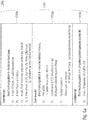
- FIG. 11 shows a schematic view of a structure of the output signal 1006, which has the data header or header 1008 and the useful data (payload) 1012.
- the data header 1008 includes information relating to the construction of the 3D multi-aperture imaging device.
- the information regarding the construction of the 3D multi-aperture imaging device can take into account a number of structural data, including a number of imaging modules, an assignment of the optical channels to the partial fields of view, a size and / or arrangement of the partial fields of view in the overall field of view or the like.
- the useful data 1012 include image information of the image sensor areas. This can be, for example, processed or unprocessed image sensor values.
- the image information can, for example, be available continuously for individual pixels or already sorted with respect to the overall image.
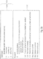
- FIG. 10 shows a schematic view of a structure of the output signal 1006, in which the data header 1008 contains the description of the 3D multi-aperture imaging device and information relating to a segmentation of the entire field of view.
- the information relating to the segmentation of the overall field of view can relate to the first or second partial fields of view of the first or second or a further module of the 3D multi-aperture imaging device.
- the information can include, for example, an indication of the number of partial fields of view in which the overall field of view is segmented, for example based on the number of optical channels arranged in the respective imaging module.
- the segmentation can be the same for at least two or all imaging modules, but can also differ from one another for at least two or all imaging modules.
- the at least two imaging modules of the 3D multi-aperture imaging device have the same structure.
- a single item of information relating to the segmentation of the field of view in the data header 1008 can be sufficient, since this information can be transferred to all imaging modules.
- at least one first imaging module is designed differently from a further imaging module, which means that the number and / or arrangement of the partial visual fields in the overall visual field differs.
- the data header 1008 can contain the information relating to the segmentation of the field of view for two, several or even all of the imaging modules of the 3D multi-aperture imaging device.
- the information relating to the segmentation of the overall field of view can thus relate to a position and / or orientation of a partial field of view in the overall field of view and / or relate to which image sensor area the partial field of view is imaged.
- the information relating to the structure of the 3D multi-aperture imaging device can relate to the number, the design, the orientation of the Imaging modules in space or also distances between the imaging modules in the 3D multi-aperture imaging device, that is to say, refer to the base distance BA.
- the description of the 3D multi-aperture imaging device may refer to the structure of the 3D multi-aperture imaging device.
- the data header 1008 can contain information about the basic spacing of the imaging modules, what number of optical channels are arranged in the array 14 1 and / or 14 2 or what order or orientation they have in space or in the imaging modules. Alternatively or additionally, a position of the imaging modules and / or an orientation of the same in space can also be specified. With a comparable design of the imaging modules, a single piece of information relating to this design can be sufficient to describe all of the imaging modules of the 3D multi-aperture imaging device.
- the processor can be designed to form the output signal in such a way that the data header 1008 has information relating to the base distance BA.
- the useful data includes pixel-by-pixel image information of the individual optical channels of the 3D multi-aperture imaging device.
- the information of the pixels of the image sensor areas of the image sensor can be arranged sequentially one after the other according to a predefined order in the useful data 1012.
- additional and / or alternative information can be arranged.
- the image information ie the pixel values
- An image format for example JPEG, Blender, IGES or the like, with and without compression, can be implemented as the processed form.
- Information relating to a three-dimensional image can be part of the useful data 1012, but also a plurality of two-dimensional images from which three-dimensional effects or information can then be derived.
- the processor 1002 can be designed to form the output signal in such a way that the useful data have information relating to the compressed image data.
- the processor 1002 can be designed, for example, to evaluate each image sensor area and thus each partial field of view sequentially one after the other and process the image information obtained from the pixels of the image sensor areas.
- the pixel-by-pixel image information of the useful data 1012 can have a structure in which each partial field of view is described one after the other in a mosaic-like manner.
- a mosaic-like shape can be obtained, for example, by interlacing the partial visual fields 74a-d in the overlapping regions 114.
- the processor 1002 can be designed to preprocess the image information of the image sensor areas, for example in order to obtain a de-mosaiced overall image.
- the processor 1002 can be designed to form the output signal 1006 in such a way that the useful data 1012 contain information relating to the overall image. For example, each column or each line of the overall image can be reproduced sequentially one after the other as image information pixel by pixel. In contrast, in the case of the mosaic-like display, each partial image can be displayed in columns or lines.
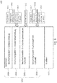
- the Figure 5a and 5b show a schematic view of a structure of the output signal 1006, which is formed by the processor 1002 by taking into account a plurality of information sources.
- the section of the data header 1008 shown is part of the in Figure 5a is shown data header 1008 and that the in Figure 5b
- the user data 1012 shown are also part of the output signal 1006, as is the one in FIG Figure 5a illustrated parts of the data header 1008.
- components 1008a, 1008b, 1008c and 1008d are shown as separate information blocks, information contained in the data header 1008 can have any structure among one another.
- the segmentation shown is for illustration purposes only and is not intended to have a restrictive effect.
- the processor 1002 can be designed to form the output signal 1006 in such a way that the data header has information relating to the number of imaging modules 11.
- the imaging modules can be designed to each completely cover the entire field of view, that is to say that the information relating to the number of imaging modules can be equated with a number of overall images of the overall field of view.
- the data header can have information about the number of optical channels per imaging module 11.
- the data header 1008 can have information about the number of pixels arranged along a first and / or second image axis that for example, can be referred to as horizontal and vertical.
- the information can relate to the number of pixels per partial image, that is to say the image sensor area, and / or the overall image of pixels recorded or arranged in the overall image.
- the processor can be designed to form the output signal 1006 in such a way that the useful data have information relating to the image sensor areas 58, for example relating to a number of pixels along a row and / or column or a geometric extent of the image sensor areas 58.
- the respective information can be identical for all imaging modules 11 and / or for the optical channels, that is to say the partial images, so that the presence of the information relating to all imaging modules and / or partial images leads to a sufficient description.
- individual information can be arranged in the data header 1008 for at least each deviating embodiment but also individually for each imaging module or partial image. This preceding description of the A) number of modules, B) number of channels per module and C) number of pixels along the image axes and / or the base distance can be arranged as a meta description with regard to the structure of the 3D multi-aperture imaging device 1000 and is shown as element 1008a of the Data headers 1008.
- the information can be inserted individually and in any combination with one another by the processor, for example an indication of a model number or the like of an imaging module or 3D multi-wallpaper imaging device can provide such information if the implementation of the module or the device is encoded thereby.
- the processor 1002 is designed to add information to the output signal 1006 about which optical channel is looking into which section of the overall field of view and / or what distance the optical channels are from one another. This can be advantageous in particular for the individual partial images in the output signal 1006.
- a geometry description that can be inserted by processor 1002 into data header 1008 of output signal 1006 is identified as element 1008b of data header 1008.
- the geometry description can relate to D) a pixel size of the pixels of the image sensor regions 58 of the image sensor 12.
- the pixels have identical or comparable sizes.
- the specification of the pixel size can thus be made globally for all pixels.
- the total number of pixels in the image sensor regions 58 has sizes that differ from one another.
- the pixel size can vary for each different implementation of the Pixel as well as for an assignment of the size to the respective pixels can be arranged in the element 1008b.
- the processor 1002 can be designed to form the output signal 1006 such that the data header 1008 has information relating to a number of pixels relating to a first image stretching direction and a number of pixels for a second image stretching direction at least for one of the image sensor areas 58 can.
- This can be, for example, the extension directions along which the partial fields of view extend in space.
- the first and second directions can be arranged perpendicular to one another and correspond to a number of rows or columns.
- the processor 1002 can be designed to E) insert two-dimensional (X / Y) or three-dimensional (X / Y / Z) coordinates for one, several or every optical channel of each module 11 or at least insert a relative positioning to one another.
- the coordinates can thus be local coordinates of an arrangement of the optical channels 16 with respect to other optical channels and / or global coordinates, i. H. an arrangement of the optical channels within the 3D multi-aperture imaging device. In both cases, an arrangement of the optical channels 16 in the module 11 and / or in the 3D multi-aperture imaging device 1000 can be described.
- the processor 1002 can be designed to form the output signal 1006 such that the data header 1008 has information relating to a spatial coordinate of the at least one optical channel 16 in the 3D multi-aperture imaging device 1000 for at least one of the optical channels 16.
- the output signal 1006 can be formed in such a way that it contains information about a geometric arrangement of the optical channels.
- the element 1008b of the data header 1008 can furthermore be formed by the processor 1002 in such a way that it comprises information F) relating to a field angle range of at least one optical channel or also the imaging module.
- the field angle range can be specified as an interval along one, preferably along two, image directions. This can also be referred to as "reaching from ...... to ..""or viewing direction ⁇ xy".
- the field angle range can be indicated by a central direction of the module 11 or the optical channel 16 and can be supplemented by an extension of the field angle range along the at least one, preferably two, image axes.
- the data header 1008 can alternatively or additionally comprise an optional element 1008c, which has information G) about environmental conditions of the 3D multi-aperture imaging device 1000.
- an optional element 1008c which has information G) about environmental conditions of the 3D multi-aperture imaging device 1000.
- a print of an atmosphere or environment surrounding the 3D multi-aperture imaging device, an ambient temperature of the 3D multi-aperture imaging device, an operating temperature of the 3D multi-aperture imaging device, a time of the image acquisition or the generation of the output signal 1006 and / or a position of the 3D multi-aperture imaging device in the Data header 1008 can be inserted.
- the location can be determined, for example, by means of a position determination system such as GPS, Galileo or Glonass, or it can be provided by an external data source such as a sensor.
- the processor can be designed to form the data header 1008 such that the element 1008c has camera-specific information relating to at least one auto focus drive.
- the at least one autofocus drive can, for example, have been used to focus the captured image.
- the camera-specific information can include an indication of a focusing of the image information or useful data. This can be a focusing used jointly for all modules, ie an autofocus drive, for a module-specific focusing, ie at least two autofocus drives, or a channel-specific focusing, ie a plurality of autofocus drives.
- the information can be the specification of a global or relative position of an element of the autofocus drive and / or a controlled variable, for example a current variable or a voltage variable for controlling the autofocus drive. The global or relative position can be reconstructed from the controlled variable, so that conclusions can be drawn about the focusing.
- the data header 1008 of the output signal 1006 may further, as shown in FIG Figure 5b is shown, have an optional element 1008d, which has information relating to possible corrections.
- the element 1008d and thus the data header 1008 can contain information relating to H) indication of at least one optical channel of the 3D multi-aperture imaging device, relating to I) vignetting, i. H. shadowing of the overall image or partial image towards the edge of the image, and / or information about J) defective pixels on the image sensor or image sensor areas 58.
- H) indication of at least one optical channel of the 3D multi-aperture imaging device relating to I) vignetting, i. H. shadowing of the overall image or partial image towards the edge of the image, and / or information about J) defective pixels on the image sensor or image sensor areas 58.
- H) vignetting i. H. shadowing of the overall image or partial image towards the edge of the image
- J defective pixels on the image sensor or image sensor areas 58.
- Each of the information H), I) and J) can also be used later to correct the image .
- the user data 1012 can, as it is in connection with the Fig. 4 is described by K) comprise image data pixel by pixel.
- identifying information relating to the pixels can be specified continuously, for example according to an option a) color information.
- Based on an image sensor used for example an assignment of four color values per pixel according to a red-green-green-blue scheme, for example according to a Bayer filter or according to a red-green-blue-white arrangement or the like.
- the respective color information and / or brightness information can be arranged continuously for consecutive pixels in the useful data 1012.
- the color information can also be arranged by the processor 1002 following a different, reconstructable scheme.
- the image data can also have pixel-by-pixel depth data, have information about a segmentation of pixels into pixel clusters and / or have information about depth information and / or distance information with regard to pixel clusters.
- the image data can be arranged in the user data, sorted by clusters, and the depth data or the cluster information can be arranged accordingly in the data header.
- the pixel values can optionally be arranged consecutively without separating information, break information or intermediate information, for example if the size of each image can be derived from the header data, for example using information C).
- a start / stop character sequence can be arranged between the pixel values or between some pixel values.
- the start / stop character string can comprise at least one bit and indicate that a new section of the image begins, for example a new partial image, a new image column or a new image line. This means that the user data contains information relating to a line break or a column break of the captured image. This can be advantageous if the aforementioned information C) is absent in the header data.
- information can be inserted in the header data for each group of pixels which enables the imaging module 11 and the optical channel 16 to be identified, that is to say an assignment of the pixels to the module 11 and the optical channel 16, as is possible is indicated by option L) c).
- the image data can be arranged in the useful data 1012 as M) a) raw data (RAW) and / or as M) b) compressed image data and / or as M) c) demosaiced image data.
- the image data can have pixel-by-pixel depth data, have information about segmentation of pixels into pixel clusters and / or have information about depth information and / or distance information with regard to pixel clusters.
- FIG. 11 shows a schematic overview of the output signal 1006 that the elements 1008a-1008d of the data header 1008 can have.
- design data 1015 of the 3D multi-aperture imaging device (3D MAAV) can be taken into account by processor 1002. This can include, for example, the pixel size D).
- calibration data 1016 can also be used by processor 1002, for example by processor 1002 reading them from a data memory.
- the calibration data for example the field angle range F), can be the same over a series of identically or identically constructed multi-aperture imaging devices.
- individual calibration data 1018 can also be used by the processor 1002, such as calibration data that are individual for the 3D multi-aperture imaging device, such as the actual coordinates E) of the optical channels in the 3D multi-aperture imaging device. For example, manufacturing tolerances can be compensated for.
- design data 1015 ' can be used by processor 1002 to the effect that distortion H) of the optical channels and / or vignetting I) are taken into account.
- this data or information H) and / or I) can also be used as calibration data 1016 ', which are identical for the series of 3D multi-aperture imaging devices.
- calibration data 1018 ′ can be used by the processor 1002 are, for example, by measuring the pixels in order to recognize the defective pixels J) and to take this into account in the useful data and / or in the correction data 1008d.
- the output signal 1006 can for example be stored as a file or data block in a memory or transmitted as a signal.
- a number of optical channels per image a number of modules and / or a number of horizontal and vertical pixels per partial image can be specified globally for all modules 11 in the data header 1008.
- the number of modules can be a number of quasi-redundant images that represent a multiplicity of the views. For example, with a number of two modules, a stereo recording can be obtained, with a number of three modules a triplet recording and with a number of four modules a quattro recording. Alternatively, several, i. H. more than four imaging modules or multi-aperture imaging devices can be arranged.
- the 3D multi-aperture imaging device has three multi-aperture imaging devices, i. H. Module, so it comprises, for example, a third plurality of optical channels for mapping each other and with the first partial fields of view overlapping third partial fields of view of the total field of view on third image sensor areas of the image sensor, the first and the second plurality of optical channels laterally by a base distance from one another are arranged offset.
- the processor is designed to receive image sensor data from the image sensor which have information about the third partial fields of view mapped onto the third plurality of image sensor areas, and is designed to provide the output signal so that the useful data from the pixels of the first image sensor areas, the second Image sensor areas and the third image sensor areas have obtained image information.
- the information in the data header can relate to a structure or an arrangement of the three modules. Alternatively, as already described, a higher number of modules is also possible.
- a number of modules for at least two modules 11 or for each module 11 a number of optical channels per image and / or a number of pixels horizontally and vertically per partial image can be specified, for example if the modules are different from one another.
- Individual and global information regarding the modules can also be arranged jointly in the output signal 1006, which can lead to redundant information reproduction.
- the geometry data 1008b of the channel arrangement can relate to a number and / or designation of the module, a number and / or designation of the optical channel in the respective module 11, a two-dimensional or three-dimensional coordinate of the channel or module and / or an angular orientation at least of an optical channel in the 3D multi-aperture imaging device.
- the geometry data can be derived and / or provided based on knowledge of the design data, for example in a memory. Alternatively, the geometry data can also be determined by a measurement, which can lead to an at least partial compensation of manufacturing tolerances.
- the geometric data can also be dependent on external influencing variables such as temperature and pressure. Knowing these variables during further image processing or image reconstruction enables a correspondingly adapted correction to be carried out.
- camera information for example relating to a manufacturer, a model, an aperture number, an exposure time, an ISO value, a light value, a focal length, a flash use and / or a flash intensity
- the camera information can have information on position data or specification of a controlled variable (control current, control voltage) of the autofocus drives.
- the geometry data 1008b can also specify a channel-by-channel, that is to say for each optical channel, a field angle range and / or a central field or viewing direction as well as an extent (horizontal / vertical) of the field angle along the image axes.
- the field angle data can be design data.
- the field angle data can also be measured in the course of a calibration, wherein the calibration can be determined on the specific structure or can correspond to typical values that are determined on a representative specimen.
- additional parameters such as pressure and temperature can be included for the selection or calculation of the data set, the data sets being obtained from design data or from calibration, the calibration being determined on the specific structure and corresponding to typical values that are used on a representative specimen were determined.
- the geometry data 1008b can alternatively or additionally have a number of rows and / or columns per optical channel, likewise globally or individually per channel. Alternatively or additionally, an indication of the pixel size can be inserted by processor 1002.
- the element 1008d may have additional environmental conditions such as pressure, temperature, time, or location. Such information can be obtained by connecting the processor 1002 to external sensors through the in the Fig. 6 sensor data 1022 shown can be obtained from processor 1002.
- the optional element 1008d can contain correction data for the optics.
- design data relating to the optical and / or perspective (Keystone's) distortion can be accessed by the processor 1002 and processed by the processor 1002.
- measured data from a calibration can be processed, the calibration being determined on the specific structure or corresponding to typical values that were determined on a representative example of a 3D multi-aperture imaging device.
- the useful data 12, that is to say the payload, can have image data for each image. Fixed, predetermined numbers of rows and / or columns can be taken into account here. Alternatively, for example start / stop bits can be arranged. Alternatively or additionally, the module and / or the channel can be identified.
- the image data can be arranged in the user data 1012 as RAW, as compressed or packed image data, such as JPEG or the like, and / or as a demosaiced image.
- Various files with geometry data, correction data and payload can also be generated by the processor 1002, which means that the output signal 1006 can be generated in a disjointed manner.
- the output signal 1006 can also be generated such that a separate payload file is output by the processor 1002 for each optical channel. It should be mentioned here that the channel-wise or cluster-wise depth information can also be inserted into the data header 1008 by the processor 1002 in the form of geometry data.
- FIG. 10 shows a schematic view of a multi-aperture imaging device 2000 according to a second aspect of the exemplary embodiments described herein, which can be arranged, for example, as an imaging module 11 in the 3D multi-aperture imaging device 1000.
- the multi-aperture imaging device 2000 is designed to image the partial fields of view 74a-74d onto the image sensor 12 by means of the optical channels 16a-16d, which each have at least one optical system or lens 64a-64d.
- the array 14 is arranged, for example, along the line extension direction 146.
- the optical channels 16a-16d are thus arranged in a one-dimensional array 14, which means that the optical channels 16a-16d are arranged, for example, in a single line.
- the overall field of view 72 can extend in space along a first image direction 142 and along a second image direction 144, wherein the directions 142 and 144 can be perpendicular to one another.
- the partial visual fields 74a-74d can be arranged next to one another and overlapping one another along the direction 142, so that an expansion of the image in the direction 144 is determined by the number of pixels and / or by the field angle of the optical channels 16a-16d along the direction 144 and the Expansion of the image along the direction 142 is influenced or determined by the number of pixels and the field angle of the optical channels 16a-16a along the direction 142 and also by the number of partial fields of view 74a-74d and the overlap factors.
- the plurality of optical channels 16a-16d form the one-dimensional array 14, which is arranged in space along the direction 144 and 146, while the partial fields of view 74a-74d of the total field of view also form a one-dimensional array that is perpendicular along the direction 142 to the direction 144 is arranged.
- the multi-aperture imaging device 2000 can thus have the feature that a conversion takes place between an arrangement direction of the array 14 and an arrangement of the corresponding partial fields of view 74a-74d in space. This can take place, for example, through a respective viewing direction of the optical channels 16a-16d.
- the multi-aperture imaging device 2000 can have a beam deflecting device (not shown) that performs such a deflection.
- the multi-aperture imaging device 2000 can advantageously be arranged in systems in which images are essentially acquired that have a significantly larger extent along a first image direction 142 compared to a second image direction 144.
- This can apply, for example, to camera systems in vehicles that cover a travel path of the vehicle in a horizontal direction capture. That is, the direction 142 can be a horizontal direction, for example.
- the optical channels 16a-16d may be arranged along a vertical direction in the vehicle. It goes without saying that the directions 142 and 146 are mutually interchangeable, which means that the information horizontal and vertical should not have any restrictive effect.
- the multi-aperture imaging device 2000 can be arranged in at least two versions as modules 11a and 11b in the 3D multi-aperture imaging device 1000.
- the 3D multi-aperture device can have fewer or more than 4 channels, but at least two.
- FIG. 3 shows a schematic block diagram of a device 3000 for processing the output signal 1006.
- the device 3000 can have a wireless or wired interface 1023 for receiving the output signal 1006.
- the signal 1006 is therefore referred to as the input signal for the device 3000.
- the device 3000 comprises a processor 1024 for processing the user data 1012 of the input signal 1006, taking into account the information relating to the structure of the 3D multi-aperture imaging device 1000 for at least first image sensor information of a partial field of view 74 11 - 74 24 of the first module 11a and a partial field of view 74 21 - 74 24 of the second module 11b.
- the processor 1024 can be designed to process other or additional information from the data header 1008.
- a function that can be implemented by the processor 1024 is, for example, a subsequent change in the focus of varying areas in the image data that are contained in the useful data 1012 of the input signal 1006.
- the device 3000 can be designed to output an image signal 1026 which enables the post-processed image data to be displayed.
- the signal 1026 can be shown on an optional monitor 1028 or display 1028.
- the signal 1026 can also be transmitted by wire or wirelessly, for example to another device.
- the other device can be a further processing device or a memory element.
- the device 3000 can be designed to process the output signal even if it indicates that a number of more than two modules have been used to capture the entire field of view.
- the functions of the process 1024 can also be implemented in the processor 1002, which means that the processors 1002 and 1024 can be designed alternately to carry out the functions described in relation to the other processor 1024 and 1002, respectively.
- the recorded image data of the 3D multi-aperture imaging device 1000 can thus be stored in a format that enables the calculation of three-dimensional object data and the subsequent, that is, after the actual image recording, the object distance-dependent definition of the areas to be focused.
- the data format can consist of a header and a payload area or at least have these.
- Descriptive data of the image-recording multi-aperture imaging system and possibly additional sensor data can be listed in the header area, whereas essentially the pixel-by-pixel image data can be listed in the payload area.
- Multi-aperture imaging systems thus obtained may have a linear channel arrangement, i.e. H. single-line arranged optical channels, and have a small or even minimal size.
- the aspects described above enable adaptable three-dimensional image recording and display.
- the depth of field can be defined subsequently.
- multi-aperture imaging devices and 3D multi-aperture imaging devices which can each be combined as additional features with the features of the 3D multi-aperture imaging device 1000.
- the multi-aperture imaging devices described below can be arranged in the 3D multi-aperture imaging device 1000 as an imaging module.
- Figure 9a shows a schematic side sectional view of a device 10 according to an embodiment in a first operating state.
- the device 10 can be a mobile or immobile device, such as a mobile phone, a smartphone, a mobile computer such as a tablet computer and / or a mobile music player.
- the device 10 comprises a multi-aperture imaging device 11 which has an image sensor 12, an array 14 of optical channels 16 arranged next to one another, and a beam deflecting device 18.
- the beam deflecting device 18 is designed to deflect a beam path 17 of the optical channels 16 and will be described in detail later.
- the device 10 comprises a housing 22 which has outer surfaces 23 which enclose a housing volume 24. That is, the housing volume 24 can comprise an inner volume of the housing 22 and the volume of the housing 22.
- the housing volume also includes a volume that is stressed by the housing walls and is thus enclosed by the outer surfaces 23 of the housing.
- the housing 22 can be made transparent or opaque and comprise, for example, plastic materials and / or metal materials.
- the beam deflecting device 18 has a first position within the housing volume 24.
- the housing 22 and / or components arranged in the housing 22 can block the beam path 17 of the optical channels 16 after being deflected by the beam deflecting device 18, so that a field of view 26 arranged outside the housing 22 should not be captured with the multi-aperture imaging device 11 or only to a limited extent is detectable.
- the components can be, for example, a battery, circuit boards, non-transparent areas of the housing 22 or the like. In other words, instead of a previous camera lens, another, possibly non-optical component can be arranged on a housing.
- the housing 22 can have an opening 28 through which the housing volume 24 is connected to an outer volume 25 of the housing 22.
- the opening 28 can temporarily be completely or partially closed by a cover 32.
- the first operating state of the device 10 can be an inactive operating state of the multi-aperture imaging device 11, in which the optical channels 16 are, for example, deflected onto the inside of the housing 22 or are not deflected.
- the overall height of the structure of the multi-aperture imaging device is at least partially determined by the diameter of the optics of the optical channels 16 (lenses).
- the extent of the mirror (beam deflection device) in this thickness direction is equal to the extent of the lenses in this direction.
- the beam path of the optical channel 16 is through the mirror 18 circumcised. This leads to a reduction in image brightness, this reduction being dependent on the field angle.
- the present exemplary embodiments solve this problem in that parts or the entire multi-channel camera structure is moved so that, in the operating state of the camera, parts of the structure via the housing z. B. a smartphone stand out compared to the state of not using the camera.
- the movement of the parts can be rotative (unfold or unfold), translative (extend) or a mixed form. Similar to known zoom lenses on compact cameras, the additional movements of parts or the entire system enable a minimal design in the non-use mode of the cameras and a larger design optimized for the implementation of the technical function in the use mode of the camera.
- Figure 9b shows a schematic side sectional view of the device 10 in a second operating state.
- the beam deflecting device 18 has a second position outside the housing volume 24. This enables the beam deflecting device 18 to deflect the beam paths 17 of the optical channels 16 outside the housing volume 24 and the field of view 26 outside the housing 22 can be detected by the multi-aperture imaging device 11.
- the cover 32 can be from the in Figure 1a be moved away from the position shown, so that the beam deflection device 18 is movable through the opening 28 of the housing 22 out of the housing volume 24.
- the beam deflection device 18 can be moved translationally and / or rotationally between the first position and the second position. It is advantageous that the components within the housing 22 and / or the housing 22 do not block the deflected beam path 17 of the optical channels 16.
- the multi-aperture imaging device 11 can be arranged in a camera housing, which in turn is arranged at least partially in the housing 22.
- the camera housing can, for example, at least partially from a carriage, as it is in connection with Fig. 13 is described, be formed. This differs from a concept in which a single-channel camera is oriented in different directions by means of a flip-over mechanism, in that in the present case a rotation or tilting of an image sensor and / or the imaging optics can be avoided.
- Figure 10a shows a schematic side sectional view of a device 20 according to a further exemplary embodiment in a first operating state.
- the device 20 has the cover 23 which is rotatably mounted on the housing 22, for example via a connecting element 34a and / or via an optional connecting element 34b.
- the connecting element 34a and / or 34b can be designed to enable tilting and consequently a rotational movement between the cover 23 of the beam deflecting device 18 relative to the housing 22 and can be designed, for example, as a hinge or roller bearing.
- the beam deflecting device 18 can form a cover of the housing or be a part thereof. One of the beam-deflecting surfaces of the beam deflector 18 can be an outer edge of the housing.
- the beam deflecting device 18 has a first position and partially or completely closes the housing 22.
- the beam deflecting device 18 can have a reflective area for deflecting the beam path 17 and have contact areas which are designed to form mechanical contact with the housing 22 in the first position.
- the camera may not be visible or barely visible when it is not in use.
- Figure 10b shows a schematic side sectional view of the device 20 in a second operating state.
- the beam deflection device 18 can be moved in a rotational manner with respect to the housing 22, that is to say folded out, so that the housing volume 24 is open.
- the rotational tilting enables an inclined or tilted orientation of the beam deflecting device 18 with respect to a course of the beam path 17 of the optical channels 16 between the image sensor 12 and the beam deflecting device 18, so that the beam path 17 is deflected at the beam deflecting device 18 in a first direction 19a.
- the connecting elements 34a and 34b can, for example, be connected to a frame structure and the beam deflecting device 18, so that the beam deflecting device 18 can alternately have the second or third position.
- a switchable viewing direction of the multi-aperture imaging device previous solutions, particularly in smartphones, can be replaced by a structure using two cameras with a viewing direction forwards and backwards.
- Figure 11a shows a schematic side sectional view of a device 30 according to a further exemplary embodiment in the first operating state.
- the device 30 has an at least partially transparent cover 36 which is arranged between an outer edge 23 of the housing 22 and the multi-aperture imaging device 11.
- the at least partially transparent cover is connected to the beam deflecting device 18 and is designed to move based on a movement of the beam deflecting device 18.
- the at least partially transparent cover 36 can comprise, for example, polymeric and / or glass materials.
- u. a. Devices can be provided which enable the optics to be encapsulated to protect against contamination with the possibility of changing the encapsulated volume (movable cover glasses).
- Figure 11b shows a schematic side sectional view of the device 30 in the second operating state.
- the at least partially transparent cover is at least partially moved out of the housing volume 24. This can take place by a rotational movement of the beam deflection device around the connecting element 34.
- the beam deflecting device 18 is designed to deflect the beam path 17 of the optical channels 16 such that the optical channels run through the at least partially transparent cover.
- the cover 36 is designed to reduce or prevent the entry of particles, dirt and / or moisture into the housing volume 24.
- the cover 36 can be made transparent for the beam paths 17 and / or can be made partially opaque. E.g. the cover 36 can be more electromagnetic for certain wavelength ranges
- the advantage of the cover 36 is that, due to the reduced amount of particles, dirt and / or moisture, a long service life of the device and / or a permanently high image quality can be obtained, since there is little soiling of the optics of the optical channels.
- Figure 11c shows a schematic side sectional view of the device 30, in which the beam deflection device 18 with an optional actuator 38 translationally along a direction y perpendicular to a direction x of the beam path 17 between the image sensor 12 and the optical channels 16 and perpendicular to a direction z perpendicular to a line extension direction of the array of optical channels 16 is movable.
- the beam deflection device 18 can also be moved in a translatory manner based on the rotational movement around the connecting element 34, for example via a guide, a lever or the like.
- the opening (rotational movement) can be done manually or using an actuator.
- the optional actuator 38 can be arranged on the beam deflecting device 18.
- the actuator 38 can be arranged between the housing 22 and the beam deflecting device 18.
- the actuator 38 can be arranged, for example, between the housing 22 and the connecting element 34a and / or between the connecting element 34a and the beam deflecting device 18. The advantage of this is that the translational movement of the beam deflecting device along the x-direction of the housing allows the housing 22 to reduce shading of the field of view to be recorded.
- Figure 12b shows a schematic side sectional view of the device 40 in the second operating state.
- the beam deflection device is moved out of the housing volume 24 based on the translational movement 42, for example along the x direction.
- the beam deflecting device 18 can be moved through the opening 28.
- the beam deflection device 18 can be rotatably movable about an axis of rotation 44.
- the beam deflecting device 18 can execute a rotary movement about the axis of rotation 44.
- An angular orientation of the beam deflection unit can be compared with the first operating state Figure 12a be changed, so that the area of the beam deflection device used by the beam path of the multi-aperture imaging device increases compared to the first operating state.
- a rotational movement 46 about the axis of rotation 44 enables a variable inclination of the beam deflector 18 relative to the beam path 17 between the optical channels 16 and the beam deflector 18 and therefore a variable direction in which the beam path 17 of the optical channels 16 is deflected.
- the optical channels 16 can have optics 64a-b.
- optics 64a-b of the optical channels 16 and / or the image sensor 12 can be arranged outside the housing volume 24 in the second operating state. E.g. the optics 64a-b of the optical channels 16 and / or the image sensor 12 can be moved along with the beam deflection device 18.
- the beam deflecting device can be movable between at least a first position and a second position, the beam paths being deflected in different directions in each position. Similar to how it is for the positions of the beam deflector 18 in the Figures 10a-c is described, the beam deflection device can also be moved about an axis of rotation. In addition to the translational movement of the housing cover 32 and the beam deflecting device 18, parts or all additional components of the multi-aperture imaging device can also be moved translationally in the same direction, with the same or different adjustment paths being possible.
- FIG. 11 shows a schematic side sectional view of a device 50 in which the cover 32 is arranged on a housing side 22b of the housing 22 such that it can move in rotation via a movement element 34.
- the beam deflecting device 18 can be mechanically connected to a displacement slide 47.
- the moving slide 47 can be understood as a mechanical transport device for moving at least the beam deflecting device 18.
- the device 50 can comprise an actuator 33 which is designed to move the displacement slide 47 in a translatory manner.
- the actuator can comprise any drive, for example a stepping motor, a piezoelectric drive or a moving coil drive.
- the device 50 can comprise an actuator 33 ′ which is designed to release a mechanical lock 35 which locks the cover 32 and the housing on at least one housing side 22a.
- the beam deflecting device or the carriage 47 can be moved out of the housing by means of spring force when the lock 33 'is released.
- the lock 35 can be designed to hold the beam deflecting device 18 in the first position.
- the carriage 47 can also be arranged in the device 40. This means that the carriage 47 can also be used with a translational movement of the cover 32.
- Figure 13b shows a schematic side sectional view of the device 50 in which the carriage 47 is moved along the translational movement direction 42, so that the beam deflection device 18 is moved out of the housing volume 24.
- the image sensor 12 and / or optics of the optical channels 16 can also be mechanically connected to the carriage 47 and can be moved along with the beam deflecting device 18 to the same extent.
- the image sensor 12 and / or the optics of the optical channels 16 can be moved to a lesser extent than the beam deflecting device 18, so that a distance between the image sensor 12, the optics and / or the beam deflecting device 18 is increased during an extension.
- the image sensor 12 and / or the optics of the optical channels can be arranged in a stationary manner with respect to the housing, so that only the beam deflection device 18 is moved by means of the displacement slide 47.
- An increasing distance between the image sensor 12, the optics and / or beam deflecting device 18 while moving out allows a small distance between the components in the first operating state, so that the multi-aperture imaging device can be accommodated in the housing 22 with little space requirement.
- Figure 13c shows a schematic side sectional view of the device 50 in the second operating state.
- the beam deflecting device can be mounted in a rotary manner in order to carry out the rotational movement 46, as is described, for example, for the device 40. How it's related to Figure 12b is described, the angular orientation of the beam deflector 18 compared with the first operating state Figure 13a or the state in Figure 13b be changed, so that the area of the beam deflection unit used by the beam path of the multi-aperture imaging device increases compared to the first operating state.
- a side of the beam deflection device 18 facing the optical channels 16 or the image sensor 12 can have a dimension B perpendicular to the translational movement direction 42, for example along the y-direction, which is greater than a dimension A of the image sensor 12 or the optical Channels 16 along this direction.
- the dimension B is, for example, perpendicular to a line extension direction of the array and parallel to a surface of an image sensor on which the optical channels impinge. This can lead to a high degree of light being deflectable by the steel deflecting device 18 and a brightness of an image to be recorded being high.
- the extension or dimension B is smaller than in the in Figure 13c position shown or a position in which the beam deflection device 18 directs the beam path in a different viewing direction.
- Figure 14a shows a schematic side sectional view of a device 60 according to an embodiment in the first operating state.
- the beam deflecting device 18 has the first position.
- the device 50 has at least partially transparent covers 36a and 36b, which are connected to the cover 32 and can be moved with the latter along the translational movement direction 42.
- the at least partially transparent covers 36a and 36b can each be arranged on different sides of the beam deflecting device 18 between the same and the housing 22.
- the covers 36a and 36b can be arranged partially or completely within the housing volume 24.
- the covers 36a and 36b can for example.
- Figure 14b shows a schematic side sectional view of the device 60, in which the beam deflecting device 18 has an intermediate position between the first position and the second position.
- the intermediate position of the beam deflecting device can be obtained while the beam deflecting device 18 is retracting or extending into the housing volume 24 or out of the housing volume 24.
- the beam deflecting device 18 is partially moved out of the housing volume 24.
- Figure 14c shows a schematic side sectional view of the device 60 in which the beam deflecting device 18 is in the second position, ie, the beam deflecting device 18 is, for example, completely moved out of the housing volume 24.
- the at least partially transparent covers 36a and 36b have a spacing 48 from one another which is smaller than a comparable spacing between side surfaces of the housing 22a and 22b.
- Figure 14d shows a schematic side sectional view of the device 60, in which a distance between the at least partially transparent covers 36a and 36b compared with the Figures 14a-c is enlarged.
- the at least partially transparent covers 36a and / or 36b can be movable along a translational movement direction 52a or 52b facing away from the other at least partially transparent cover 36a or 36b, for example along a positive or negative y-direction.
- the illustrated state of the at least partially transparent covers 36a and 36b can be understood as the retracted or folded state.
- the in Figure 14d The state shown can be understood as an extended or unfolded state, in which a distance 48 'between the at least partially transparent covers 36a and 36b is changed, for example increased, compared to the distance 48.
- the distance 48 ′ can, for example, be greater than or equal to the distance between the comparable sides of the housing 22.
- the beam deflecting device 18 is designed to deflect the beam paths of the optical channels so that they pass through the at least partially transparent covers 36a and / or 36b run.
- the rotational movement 46 for changing a viewing direction of the multi-aperture imaging device can be combined with a rotational movement of the beam deflecting device 18 for optical image stabilization, which is in connection with Fig. 9 is described.
- the covers 36a and / or 36b can encapsulate the other components of the multi-aperture imaging device.
- the oppositely arranged covers 36a and / or 36b or transparent areas thereof can have a switchable screen, so that the switchable screen is introduced, for example, above and / or below or along any other direction of the beam deflecting device.
- the aperture can be switched according to the operating status and direction of view of the camera. E.g. For example, an unused viewing direction of the multi-aperture imaging device can be at least partially closed by the diaphragm in order to reduce the entry of stray light.
- the apertures can, for. B. moved mechanically or electrochromic.
- the areas influenced by the screen can also be equipped with a switchable screen that covers the optical structure in the event that it is not used.
- the screen can be electrically controllable and comprise an electro-chrome layer (sequence).
- the screen can comprise a mechanically moved part.
- the movement can take place using pneumatic, hydraulic, piezoelectric actuators, DC motors, stepper motors, thermal actuators, electrostatic actuators, electrostrictive and / or magnetostrictive actuators or drives.
- the diaphragm can be switched in such a way as to allow the beam paths of the optical channels to pass through.
- the multi-aperture imaging device can have a first operating state and a second operating state.
- the beam deflection device can deflect the beam path of the optical channels in the first operating state in such a way that it passes through a first transparent region the cover 36a extends.
- the beam path of the optical channels can be deflected so that it runs through a second transparent area of the cover 36b.
- a first screen 53a can be designed to optically at least partially close the first transparent area in the second operating state.
- a second diaphragm 53b can be designed to optically at least partially close the second transparent area in the first operating state. In this way, the entry of false light from a direction that is not the current viewing direction of the multi-aperture imaging device can be reduced, which has an advantageous effect on the image quality.
- the first and / or second diaphragm 53a-b can be effective for at least one, for at least two or for all of the optical channels.
- At least one, at least two or all of the optical channels of the multi-aperture imaging device can run through the first diaphragm when the beam path of the optical channels is directed through the first transparent area and run through the second diaphragm when the beam path of the optical channels is directed through the second transparent area becomes.
- the housing can be opened up and / or the beam deflecting device extended such that the imaging module, ie the optical channels, optics thereof and / or the image sensor are moved out of the housing volume.
- a change in the angle of the beam deflection device can make it possible for the multi-aperture imaging device to extend large in the thickness direction and / or for the beam deflection device to be able to deflect the beam path "forwards" and "backwards" without hindrance.
- Cover glasses for example the covers 36, can also be fixed with respect to the unfolded or extended elements.
- the cover glasses can have any flat or non-flat surfaces.
- FIG. 11 shows a schematic perspective view of a device 70 according to an exemplary embodiment, which has three multi-aperture imaging devices 11a-c.
- the device 70 may include the processor 1002 as described for the multi-aperture imaging device 1000.
- the multi-aperture imaging devices 11a-c can be movable translationally along a respective translational movement direction 42a-c.
- the multi-aperture imaging devices 11a-c can be arranged in secondary sides 22c-f of the housing 22.
- the housing can be made flat, which means a first extension of the housing 22 along a first housing direction, e.g. an x-direction, and a second extension of the housing 22 along a second housing direction, e.g.
- a z-direction can be at least three times that dimension, at least five times or at least seven times Dimension compared to a third extension of the housing 22 along a third housing direction, for example the y-direction.
- a main side 22a and / or 22b of the housing 22 can have the first and second dimensions and can be arranged, for example, parallel to an x / z plane in space.
- the secondary sides 22c-f can connect the main sides 22a and 22b or be arranged between them.
- the multi-aperture imaging devices 11a and 11b can be arranged in or on the same side 22d in the housing 22 and, for example, have a basic distance BA from one another, such as for the purpose of stereoscopy. More than two modules would also be conceivable.
- the overall field of view can be captured stereoscopically or at a higher level by using the multi-aperture imaging device 11c and at least one further multi-aperture imaging device 11a and / or 11b.
- the multi-aperture imaging devices 11a, 11b and / or 11c can be individually movable. Alternatively, two or more of the modules can also be moved together as an overall system.
- the device 70 can be designed to capture an overall field of view at least stereoscopically.
- the overall field of view is arranged, for example, on one of the main sides 22a or 22b, but can also be arranged on a secondary side 22c-f.
- the multi-aperture imaging devices 11a-c can each record the entire field of view.
- the multi-aperture imaging devices 11a-c are shown arranged spatially spaced from one another, the multi-aperture imaging devices 11a, 11b and / or 11c can also be arranged spatially adjacent or combined. E.g.
- the arrays of the imaging devices 11a and 11b which may be formed as a single line, can be arranged next to one another or parallel to one another, as is the case, for example, in connection with FIG Figure 21b describe is.
- the arrays can form rows to one another, each multi-aperture imaging device 11a and 11b having a single-row array.
- the imaging devices 11a and 11b can have a common beam deflection device and / or a common carrier of optics of the optical channels and / or a common image sensor.
- FIG. 8 shows an enlarged perspective view of a section of the device 70 and the multi-aperture imaging devices 11a and 11b.
- the device 70 has the second operating state.
- the multi-aperture imaging device 11a and / or 11b protrudes beyond the original housing side.
- the beam deflecting devices 18a and 18b are at least partially moved outside of the housing volume based on the translational movement directions 42a and 42b.
- only some of the beam deflection devices of the multi-aperture imaging devices 11a-c can also be moved out of the housing volume of the housing 22 in the second operating state.
- the multi-aperture imaging devices 11a-b each have, for example, four optical channels 16a-d and 16e-h.
- the beam deflecting devices 18a and 18b are each designed to deflect the beam paths 17a-d and 17e-h of the optical channels 16a-d and 17e-h, respectively.
- other multi-aperture imaging devices may have different numbers of optical channels from each other.
- the multi-aperture imaging devices 11a-b can have the same number of optical channels or a number different from one another.
- the multi-aperture imaging devices 11a and 11b each have lighting devices 54a and 54b or 54c and 54d.
- the lighting devices 54a-d are designed to at least partially illuminate the entire visual field to be captured and can, for example, each be designed to illuminate a center of the total visual field to be captured (object region).
- at least one of the lighting devices 54a or 54b or 54c or 54d can be arranged such that it illuminates the entire field of view along a central viewing direction of the optical channels 16a-d or 16e-h.
- the overall field of view can have partial fields of view which differ from one another and which are each recorded by at least one optical channel 16a-d or 16e-h.
- a mean viewing direction of optical channels 16a-d or 16e-h can be, for example, a geometric mean of the viewing directions or a median value of the viewing directions.
- the lighting devices 54a-b and 54c-d can be operated as flash light of the respective multi-aperture imaging device 11a or 11b and can include any light source.
- the light source can advantageously be embodied as a light-emitting diode (LED), for example, since it requires little space and energy.
- a multi-aperture imaging device comprise none, one or more than two lighting devices 54a-d, wherein the number of lighting devices 54a-d of a multi-aperture imaging device can be different from or the same as other multi-aperture imaging devices of a device.
- At least one of the lighting devices 54a-d can be designed to illuminate several fields of view. Thus, for example, light can be emitted by the lighting device in one or more directions.
- light sources 54i can be arranged on the front and rear of the displacement slide 47b and, depending on the position of the beam deflecting device 18b, corresponding light sources can be used. The other, opposite light sources can remain unused.
- the lighting devices 54a and 54b are arranged between the beam deflecting device 18a and the image sensor 12a of the multi-aperture imaging device 11a.
- the beam deflecting device 18 can be designed to deflect an illuminating radiation emitted by the illuminating device 54a and / or 54b, for example a flashlight.
- the lighting devices 54a-b can be arranged within the housing volume in the first operating state and in the second operating state of the device 70.
- the illumination radiation can at least partially be part of the beam paths 17a-d.
- an illumination device 54c and / or 54d can be arranged laterally next to the beam deflection device on the displacement slide 47b.
- the lighting devices 54c and 54d can be moved into the housing 22 or out of the housing 22 with the translational movement 42b.
- the lighting devices 54c and 54d can be mechanically connected to the traversing slide 47a and can thus be arranged within the volume 24 in the first operating state and therefore not visible to a user.
- the lighting devices 54a and 54b can alternatively and / or additionally be arranged in a stationary manner in the housing 22. A movement of the carriage 47b can cause a movement of the lighting devices 54c and 54d.
- optics 16a-d or 16e-f and possibly the image sensor 12a or 12b can also be moved out of the housing volume by moving the carriage 47a or 47b.
- LEDs can be attached to the moving parts to implement additional lighting (flash light).
- the LEDs can be attached in such a way that they radiate in the central direction of the channels or the beam deflection devices can provide further areas that are used to deflect the radiation.
- Fig. 17 shows a schematic perspective view of a device 90 according to an embodiment, which has the second operating state.
- the beam deflecting device 18 can be connected to the multi-aperture imaging device by means of fastening elements 56a and 56b.
- the fastening elements 56a and 56b can be part of a carriage.
- Figure 18a shows a schematic perspective view of a device 100 according to an exemplary embodiment in the first operating state.
- the cover 32 can form a plane with a main housing side and / or a secondary housing side, for example the secondary housing side 22c.
- No gap or only a small gap approximately less than or equal to 1 mm, less than or equal to 0.5 mm or less or equal to 0.1 mm, can be arranged between the cover 32 and the housing side 22c, so that a transition between the cover 32 and the housing side 22c is not or hardly noticeable. In simple terms, the cover 32 cannot be visible.
- Figure 18b shows a schematic view of the device 100 in the second operating state.
- the beam deflecting device 18 has the second position outside the housing volume. Viewed from the outside, the extended multi-aperture imaging device can be enclosed on all sides by the stationary housing frame and / or have an appearance like a button.
- the device 100 can be designed to respond to a mechanical pressure on the cover 32 according to Figure 18a to release a mechanical lock so that the beam deflection device can be moved out of the housing 22, for example based on a spring force.
- the mechanical pressure can be generated, for example, by an actuator and / or by a user, for example by pressing a finger.
- the beam deflecting device can be moved back into the first position by means of the actuator or by means of mechanical pressure and can actuate a lock there.
- the actuator can be, for example, the actuator 33 or 33 '.
- the movement can also take place manually, so that the user moves the parts or the entire system in or out or folds them in or out with his own strength.
- the movement can in particular be a combination of manual actuation and the action of spring force. So works or pushes the user manually parts or the entire system to turn off the camera into the housing of the device, such. B. a smartphone, tensions a spring and a locking mechanism holds this position.
- the camera e.g. B.
- the switchable locking mechanism is released by a suitable controllable mechanism, such as an electric relay, and the spring force of the spring causes the parts of the camera or the entire system to be extended or unfolded.
- a suitable controllable mechanism such as an electric relay
- the cover that forms part of the housing, the extendable and / or tiltable part and / or another mechanism attached thereto can be shaped in such a way that (finger) pressure on this cover releases the lock, the parts or else extend or fold the entire system and, if necessary, start the image recording software on the device.
- Figure 18c shows a schematic representation of an alternative to Figure 18a , in which the cover 32 is formed such that a continuous gap is formed between main sides of the housing 22 in the secondary side 22c. This allows only two instead of four in Figure 18a columns shown in the housing 22 are perceptible.
- the extendable or fold-out cover 32 and / or further covers can be formed as part (s) of the housing 22 on one or more peripheral sides of the flat housing.
- FIGS Figures 19a-c show a multi-aperture imaging device 11 according to an exemplary embodiment of the present application.
- the multi-aperture imaging device 11 of FIG Figures 19a-c comprises a single-row array 14 of optical channels 16a-d arranged next to one another.
- Each optical channel 16a-d includes optics 64a-d for mapping a respective partial field of view 74a-d of an overall field of view 72 of the device 11 onto a respectively assigned image sensor area 58a-d of an image sensor 12.
- the image sensor areas 58a-d can each be formed from a chip, for example which comprises a corresponding pixel array, the chips as in FIGS Figures 19a-c indicated, can be mounted on a common substrate or a common circuit board 62.
- the image sensor areas 58a-d are each formed from a part of a common pixel array that extends continuously over the image sensor areas 58a-d, the common pixel array being formed on a single chip, for example. For example, only the pixel values of the common pixel array in the image sensor areas 58a-d are then read out.
- Various mixtures of these alternatives are of course also possible, e.g. B. the presence of a chip for two or more channels and another chip for again other channels or the like.
- these can for example be mounted on one or more circuit boards, such as. B. all together or in groups or the like.
- optical channels 16a-d are arranged in one line next to one another in the direction of the line extension of the array 14, but the number four is only an example and could also assume any other number greater than one.
- the array 14 can also have further lines which extend along the direction of line extension.
- Optical axes or the beam paths 17a-d of the optical channels 16a-d run parallel to one another between the image sensor areas 58a-d and the optics 64a-d.
- the image sensor areas 58a-d are arranged, for example, in a common plane, as are the optical centers of the optics 64a-d. Both planes are parallel to each other, ie parallel to the common plane of the image sensor areas 58a-d.
- optical centers of the optics 64a-d coincide with centers of the image sensor areas 58a-d.
- the optics 64a-d on the one hand and the image sensor regions 58a-d are arranged in these parallel planes with the same repetition spacing in the direction of line extension.
- An image-side distance between image sensor areas 58a-d and the associated optics 64a-d is set such that the images on the image sensor areas 58a-d are set to a desired object distance.
- the distance is, for example, in a range equal to or greater than the focal length of the optics 64a-d or, for example, in a range between one and two times the focal length of the optics 64a-d, both inclusive.
- the image-side distance along the optical axis 17a-d between the image sensor area 58a-d and the optics 64a-d can also be adjustable, e.g. B. manually by a user or automatically via an autofocus control.
- the overall field of view direction 76 emerges from the optical axes 17a-d by rotating about the direction of line extension by an angle that is> 0 ° and ⁇ 180 ° and, for example, between 80 and 100 ° and can be 90 °, for example.
- the total field of view of the device 11, which corresponds to the total coverage of the partial fields of view 74a-d, is therefore not in the direction of an extension of the series connection of the image sensor 12 and the array 14 in the direction of the optical axes 17a-d, but rather the total field of view is to the side due to the beam deflection to image sensor 12 and array 14 in a direction in which the overall height of device 11 is measured, ie the lateral direction perpendicular to the direction of line extension.
- the beam deflecting device 18 directs each beam path or the beam path of each optical channel 16a-d with a channel-specific one Deviation from the deflection just mentioned leading to direction 76.
- the beam deflecting device 18 comprises a reflective facet 68a-d for each channel 16a-d. These are slightly inclined towards each other. The mutual tilting of the facets 68a-d is selected such that when the beam is deflected by the beam deflection device 18, the partial visual fields 74a-d are provided with a slight divergence such that the partial visual fields 74a-d only partially overlap.
- the individual deflection can also be designed in such a way that the partial fields of view 74a-d cover the total field of view 72 in two dimensions, that is to say are arranged distributed in two dimensions in the total field of view 72.
- the channel-specific deflections by the beam deflecting device 18 would again lead to the partial fields of view 74a-d only slightly overlapping one another, e.g. B. in pairs with an overlap ⁇ 10% based on the solid angle areas of the partial fields of view 74a-d.
- the beam paths or optical axes could also deviate from the parallelism described and yet the parallelism of the beam paths of the optical channels could still be so pronounced that the partial fields of view covered by the individual channels 16a-N or on the respective image sensor areas 58a-d would largely overlap without further measures, such as beam deflection, so that in order to cover a larger overall field of view by the multi-aperture imaging device 11, the beam deflection device 18 provides the beam paths with an additional divergence so that the partial fields of view of N optical channels 16a-N less overlap one another.
- the beam deflection device 18 ensures, for example, that the overall field of view has an opening angle that is greater than 1.5 times the opening angle of the individual partial fields of view of the optical channels 16a-N.
- optical axes could, for example, run in a common plane before or without beam deflection, but divergent in this, and the facets only cause an additional divergence in the other transverse plane, i.e. they are all parallel to the direction of line extension and only different from the aforementioned common plane of the optical axes inclined, whereby here again several facets can have the same inclination or could be assigned jointly to a group of channels whose optical axes differ, for example, already in the aforementioned common plane of the optical axes in pairs before or without beam deflection.
- the entire divergence could also be achieved by the lateral offset between the optical centers of the optics on the one hand and the centers of the image sensor areas on the other hand, or by prism structures or decentered lens sections.
- the aforementioned possible pre-divergence can be achieved, for example, in that the optical centers of the optics lie on a straight line along the line extension direction, while the centers of the image sensor areas are projected from the projection of the optical centers along the normal of the plane of the image sensor areas onto points on a straight line are arranged differently in the image sensor plane, such. B. at points that deviate from the points on the aforementioned straight line in the image sensor plane individually channel along the line extension direction and / or along the direction perpendicular to both the line extension direction and the image sensor normal.
- advance divergence can be achieved in that the centers of the image sensors lie on a straight line along the line extension direction, while the centers of the Optics from the projection of the optical centers of the image sensors along the normal of the plane of the optical centers of the optics on points on a straight line in the optics center plane are arranged differently, such.
- the aforementioned channel-specific deviation from the respective projection runs only in the direction of line extension, that is to say the optical axes are only located in a common plane and are provided with a previous divergence. Both optical centers and image sensor area centers then each lie on a straight line parallel to the direction of line extension, but with different intermediate distances.
- a lateral offset between the lenses and image sensors in a perpendicular lateral direction to the direction of line extension led to an increase in the overall height.
- a purely in-plane offset in the direction of line extension does not change the overall height, but there may be fewer facets and / or the facets are only tilted in one angular orientation, which simplifies the construction.
- Facets 68a and 68b can be formed by one facet and facets 68c and 68d can be formed by another facet, as shown by dashed lines between the respective pairs of facets, and the only two facets are inclined in only one direction and both parallel to the direction of line extension. It is also possible that individual facets only have a tilt in one spatial direction.
- optical channels are assigned to the same partial field of view, such as. B. for the purpose of super resolution or to increase the resolution with which the corresponding partial field of view is scanned through these channels.
- the optical channels within such a group then run parallel before beam deflection, for example, and would be deflected onto a partial field of view by a facet.
- Pixel images of the image sensor would advantageously be one Channel of a group in intermediate positions between images of the pixels of the image sensor of another channel of this group.
- the multi-aperture imaging device can have a first multiplicity of optical channels which are designed to capture an overall field of view, possibly completely.
- a second multiplicity of optical channels of the multi-aperture imaging device can be designed in order to also and possibly completely cover the entire field of view.
- the overall field of view can thus be captured at least stereoscopically through the first multiplicity of optical channels and through the second multiplicity of optical channels.
- the first plurality of optical channels and the second plurality of optical channels can encounter a common image sensor, use a common array (array optics) and / or be deflected by a common beam deflection device.
- a coherent array camera is formed which can be jointly controlled as a device, for example with regard to a focus and / or image stabilization, which is advantageous since all channels are influenced simultaneously and using the same actuators become.
- the monolithic structure results in advantages with regard to the mechanical stability of the overall arrangement, especially in the event of temperature changes. This is advantageous for the composition of the overall image from the partial images of the individual channels as well as for the acquisition of three-dimensional object data when used in stereo, triple, quattro, etc. systems with multiple scanning of the overall field of view through different multiplicity of channels 16.
- the following discussion deals with the optics 64a-d, the lens planes of which also lie parallel to the common plane of the image sensor regions 58a-d.
- lenses of the optics 64a-d of the optical channels 16a-d are attached to a main side 66a of the substrate 66 via one or more lens holders and are mechanically connected to one another via the substrate 66.
- the beam paths 17a-d of the plurality of optical channels 16a-d run through the substrate 66.
- the substrate 66 is thus formed at least in some areas from transparent material and is plate-shaped or has, for example, the shape of a parallelepiped or another convex body with a planar main side 66a and an opposite main side 66b, which is also planar.
- the flat carrier substrate 66 is, for example, a substrate made of glass or polymer.
- the carrier substrate 66 can comprise a glass plate.
- the material of the substrate 66 can be selected according to aspects of high optical transparency and low temperature coefficient or other mechanical properties such as hardness, elasticity or torsion modulus.
- the substrate 66 can be designed as a simple planar part of the beam path without any additional lenses being accommodated directly on it.
- panels such as. B. aperture or false light diaphragms, and / or filter layers, such as. B. IR-block filters can be attached to the substrate surfaces or consist of several layers of different substrates, on the surfaces of which apertures and filter layers can be attached, which in turn can be channeled z. B. can differentiate in their spectral absorption.
- the substrate 66 can consist of material that has different properties in different regions of the electromagnetic spectrum that can be detected by the image sensor, in particular a non-constant absorption.
- each optic 64a-d includes three lenses.
- the number of lenses can, however, be freely selected. The number could be 1, 2, or any other number.
- the lenses can be convex, just an optically imaging functional surface such. B. have a spherical, an aspherical, a freeform surface, or two, such as. B. two opposite one another, for example to give a convex or a concave lens shape.
- Several optically effective lens surfaces are also possible, such as B. by building a lens from several materials.
- each optic 64a-d has a further second and third lens 82a-d and 84a-d, respectively.
- These lenses are, for example, fixed to one another in the interior of the respective lens holder via axially extending tubular lens holders 86a-d and fixed to the main side 66b via the latter, e.g. B. by means of gluing or another joining technique.
- Openings 88a-d of the lens holders 86a-d are provided, for example, with a circular cross-section, in the cylindrical inside of which the lenses 82a-d and 84a-d are fastened.
- the lenses lie coaxially on the respective optical axis of the beam paths 17a-d.
- the lens holders 86a-d can, however, also have a cross section that changes over their length or along the respective optical axes.
- the cross-section can increasingly have a rectangular or square character as the distance from the image sensor 12 decreases.
- the outer shape of the lens holder can thus also differ from the shape of the openings.
- the material of the lens holder can be light-absorbing.
- the lens holders can also be not rotationally symmetrical and / or not coaxial.
- the substrate 66 it is possible for the substrate 66 to be planar on both sides and therefore not have any refractive power. However, it would also be possible for the substrate 66 to have mechanical structures, such as e.g. B. recesses or projections that allow easy, positive and / or non-positive alignment of subsequent components, such as. B. the connection of individual lenses or housing parts. In the embodiment of Figures 19a-c
- the substrate 66 on the main side 66b could have structures to facilitate fastening or to facilitate alignment at the positions at which the respective end of the tube of the Lens holder 86a-d of the respective optics 64a-d is attached.
- These structures can be, for example, a circular depression or a depression with another shape that corresponds to the shape of a side of the respective lens holder facing the substrate, into which the side of the respective lens holder 84a-d can engage. It should be emphasized once again that other opening cross-sections and, accordingly, possibly other lens apertures than circular ones are also possible.
- FIG. 19a-c So it breaks away from a classic structure of camera modules which have individual lenses and for holding the individual lenses have a non-transparent housing carrier that completely encloses them. Rather, the above embodiment uses a transparent body 66 as a substrate carrier. This extends over several adjacent optical channels 16a-d in order to be penetrated by their imaging beam path. It does not disturb the image, but it also does not increase the overall height.
- each optic 64a-d does not necessarily extend over all channels 16a-d of the multi-aperture imaging device 11.
- each optic 64a-d it would be possible for each optic 64a-d to have lenses on both sides 66a and 66b held by lens carriers, as shown in FIG Fig. 19f is shown.
- a device 92 could be present to rotate the beam deflector 18 about the axis of rotation 44 which is parallel to the line extension direction of the array 14.
- the axis of rotation 44 lies, for example, in the plane of the beam paths 17a-d or less than a quarter of a diameter of the optics 64a-d away therefrom.
- the axis of rotation is further away, such as. B. less than one optic diameter or less than four optic diameter.
- the device 92 can be provided, for example, to move the beam deflection device 18 with a short response time in only a small angular range, such as e.g. B.
- the device 92 would be controlled, for example, by an image stabilization controller.
- the device 11 can additionally or alternatively have a device 98 for changing the image-side distance between the image sensor 12 and optics 64a-d or between the image sensor 12 and the carrier 66, in order to achieve a depth of field adjustment.
- the device 98 can be controlled by a manual user control or by an autofocus control or focusing device of the device 11.
- the device 94 thus serves as a suspension for the substrate 66 and is preferably, as in FIG Fig. 20 indicated laterally next to the substrate 66 along the line extension direction so as not to increase the overall height. It also applies to devices 92 and 98 that they are preferably arranged in the plane of the optical beam paths in order not to increase the overall height.
- the device 98 can also be connected to the beam deflecting device 18 and move it simultaneously or almost simultaneously, so that when the image-side distance between the image sensor 12 and the optics 64a-d changes, a distance between the optics 64a-d and that of the beam deflecting device 18 is essentially remains constant or constant.
- the devices 92, 94 and / or 98 can be implemented on the basis of pneumatic, hydraulic, piezoelectric actuators, DC motors, stepper motors, thermal actuators, electrostatic actuators, electrostrictive and / or magnetostrictive actuators or drives.
- the optics-to-beam deflection device distance could be set to a minimum distance so that the beam path of the channels is not laterally restricted by the segments of the beam deflection device 18, which reduces the overall height, since otherwise the segments 68a-d with regard to the lateral extent for the largest optics-to-beam deflection device distance would have to be dimensioned in order not to cut into the beam path.
- the constancy of the relative position of the aforementioned frames could hold the optics and the beam deflecting device rigidly to one another along the x-axis, so that the device 94 would translate the optics 64a-d together with the beam deflecting device along the line extension direction.
- the beam deflection device 18 described above for deflecting the beam path of the optical channels, together with the actuator 92 for generating the rotational movement of the beam deflection device 18, enables an optical image stabilization control of the multi-aperture imaging device 11 an image or overall field of view stabilization in two dimensions, namely through the translational movement of the substrate 66 an image stabilization along a first image axis which runs essentially parallel to the line extension direction, and through the generation of the rotational movement of the beam deflection device 18 an image stabilization along a second Image axis, which runs essentially parallel to the optical axes in front of or without beam deflection, or - if the deflected optical axes are considered - perpendicular to the optical axes and the direction of line extension.
- the described arrangement can bring about a translational movement of the beam deflecting device fixed in the frame mentioned and of the array 14 perpendicular to the direction of line extension, such as e.g. B. by the actuator 98 described, which can be used for realizing a focus setting and thus an autofocus function.
- a translational relative movement between the image sensor 12 and the array 14 can also be implemented. This relative movement can be provided by the device 94 and / or the device 98, for example.
- the device records an image of a scene per channel when recording via the image sensor areas, which is mapped onto the image sensor areas by the channels, and that the device optionally has a processor that combines or merges the images into an overall image that corresponds to the scene in the overall field of view, and / or provides additional data, such as 3D image data and depth information of the object scene for the creation of depth maps and for the software implementation such.
- the latter tasks could also be done by that processor or externally.
- the processor could also represent a component external to the multi-aperture imaging device.
- Figure 21a illustrates that devices 11 of the alternatives described above can be installed, for example, in a flat housing of a portable device 130, such as a mobile phone, a smartphone or media player or the like, in which case the planes of the image sensor 12 or the image sensor areas and the lens planes, for example of the optics of the optical channels 16 perpendicular to the flat extension direction of the flat housing or parallel to the thickness direction.
- the beam deflecting device 18 would ensure that the entire field of view of the multi-aperture imaging device 11 lies in front of a front side 102 of the flat housing, which, for example, also has a screen.
- a deflection would also be possible in such a way that the field of view is located in front of a rear side of the flat housing that is opposite the front side 102.
- the housing 22 of the device 130 or the device itself can be flat, since the illustrated position of the device 11 in the housing means that the overall height of the device 11, which is parallel to the thickness of the housing, can be kept low.
- Switchability could also be provided by providing a window on the side opposite side 102 and, for example, moving the beam deflecting device between two positions, in that the latter is designed, for example, as a front and rear reflecting mirror and rotated from one position to the other or as a facet mirror with one set of facets for one position and another set of facets for the other position, the sets of facets lying next to one another in the direction of line extension and switched between the positions by translatory back and forth movement of the beam deflector along the direction of line extension becomes.
- An installation of the device 11 in another possibly non-portable device, such as. B. a car would of course also be possible.
- modules 11 whose partial fields of view of their channels cover the same field of view completely and optionally even in a congruent manner, can with a base distance BA (cf. Fig. 15 ) be installed in the device 130 in relation to one another along a line extension direction which is the same for both modules, for example for the purpose of stereoscopy. More than two modules would also be conceivable.
- the line extension directions of the modules 11 could also not be collinear, but merely parallel to one another.
- a device 11 or a module could also be equipped with channels in such a way that they completely cover the same overall field of view in groups.
- the modules can be arranged in one or more row (s) / row (s) or at any point on the device. In the case of an arrangement of several modules, these can be formed identically or differently.
- a first module can be designed to carry out a stereoscopic acquisition of the entire field of view.
- a second module can be designed to carry out a simple acquisition, a stereoscopic acquisition or a higher-order acquisition.
- the beam deflection device could also be absent in alternative exemplary embodiments compared to the exemplary embodiments described above. If only partial mutual overlap of the partial fields of view is desired, then this could be achieved, for example, by mutual lateral offsets between the center of the image sensor area and the optical center of the optics of the corresponding channel.
- the actuators according to _ Fig. 20 could of course still be used, with the actuator 94 being able to replace the device 92, for example, in addition to a translational movement of the optics or the carrier 66.
- the above embodiments thus show a multi-aperture imaging device with a single-line array of optical channels arranged next to one another, in which somewhere in the beam path of the multi-aperture imaging device a substrate made of, for example, glass or polymer extends over the channels to improve stability.
- the substrate can also contain lenses on the front and / or back.
- the lenses can consist of the material of the substrate (such as created by hot stamping) or be molded on it.
- front of and behind the substrate there can be additional lenses which are not located on substrates and which are mounted individually.
- a plurality of substrates can be present in one structure, both along and perpendicular to the direction of line extension.
- lenses that are attached to the main sides 66a and / or 66b via lens holders, but is shown here as an example made in one piece by injection molding or the like, for example that lenses are formed on the two sides 66a and 66b, just as, of course, molded lenses of other material than the material of the parallelepiped-shaped substrate 66 would be possible as well as lenses on only one of the sides 66a or 66b. Both substrates are transparent and are penetrated by the beam paths, namely through the main sides 66a and 66b.
- the above embodiments can thus be implemented in the form of a multi-aperture imaging device, with a single-line channel arrangement, wherein each channel transmits a partial field of view of a total field of view and the partial fields of view partially overlap.
- a structure with several of such multi-aperture imaging devices for stereo, trio, quattro, etc. structures for 3D image recording is possible.
- the plurality of modules can be designed as a coherent line.
- the contiguous line could use identical actuators and a common beam deflecting element.
- One or more mechanically reinforcing substrates that may be present in the beam path can extend over the entire line, which can form a stereo, trio, quattro structure.
- Super-resolution methods can be used, with several channels mapping the same partial image areas.
- the optical axes can also run divergent without a beam deflection device, so that fewer facets are required on the beam deflection unit.
- the facets then advantageously have only one angle component.
- the image sensor can be in one piece, have only one contiguous pixel matrix or several interrupted ones.
- the image sensor can be composed of many sub-sensors which, for. B. are arranged side by side on a circuit board.
- An autofocus drive of a focusing device can be designed such that the beam deflecting element is moved synchronously with the optics or is stationary. In the absence of an advance divergence, exemplary embodiments provide that the beam paths between the image sensor 12 and the beam deflecting device 18 run essentially or completely parallel.
- Figure 21b shows a schematic structure comprising a first multi-aperture imaging device 11a and a second multi-aperture imaging device 11b, as it can be arranged in the device 130, for example.
- the two multi-aperture imaging devices 11a and 11b can form a common multi-aperture imaging device 11 and have a common image sensor 12 and / or a common array 14.
- the single-line arrays 14a or 14 1 and 14b or 14 2 form, for example, a common line in the common array 14.
- the image sensors 12a and 12b can form the common image sensor 12 and, for example, on a common substrate or on a common circuit carrier such as a common circuit board or a common flexboard.
- the image sensors 12a and 12b can also comprise substrates that are different from one another.
- Different mixtures of these alternatives are of course also possible, such as multi-aperture imaging devices comprising a common image sensor, a common array and / or a common beam deflection device 18 as well as further multi-aperture imaging devices which have separate components.
- a common image sensor a common one single-line array and / or a common beam deflection device is that a movement of a respective component can be obtained with great precision by controlling a small number of actuators and a synchronization between actuators can be reduced or avoided. Furthermore, high thermal stability can be obtained.
- further multi-aperture imaging devices can also have a common array, a common image sensor and / or a common beam deflection device.
- the structure of the multi-aperture imaging device 11 can be used, for example, for a stereoscopic acquisition of a total or partial field of view when optical channels of different partial multi-aperture imaging devices 11a and 11b are directed onto the same partial field of view.
- further partial multi-aperture imaging devices can be integrated into the common multi-aperture imaging devices, so that a higher-order acquisition is possible compared to stereo.
- Figure 22a shows an embodiment of a multi-aperture imaging device 150.
- the image sensor areas 58a-d are preferably arranged in a common plane, namely the image plane of the optical channels 16 or their optics.
- this plane is exemplarily parallel to the plane that is spanned by a z- and a y-axis of a Cartesian coordinate system that is shown in Figure 22a is drawn in and provided with the reference symbol 115 to simplify the following description.
- the size extension of the multi-aperture imaging device 150, as it is limited downward by the image sensor 12 and the optics 64, along the line extension direction is greater than the diameter of a lens.
- the minimum dimension of the multi-aperture imaging device 150, as determined by the mutual arrangement of image sensor 12 to form optics 64 along the z-axis, ie along the optical axes or beam paths of optical channels 16a-d, is smaller than the minimum dimension along the z-axis, but due to the configuration of the optical channels 16a-d as a single-line array, it is greater than the minimum dimension of the multi-aperture imaging device in the lateral direction y perpendicular to the line extension direction z.
- each individual optical channel 16a-d such as. B. the extension of the optics 64a-d along the y-axis, possibly including the holder 66, given.
- the optical axes 17a-d in front of or without the deflection by the beam deflecting device 18 or at, for example, the optics 64a-d parallel to one another, as shown in FIG Figure 22a is shown, or they differ only slightly.
- the corresponding centered positioning of optics 64a-d and image sensor areas 58a-d is easy to produce and inexpensive in terms of minimizing the installation space.
- the parallelism of the beam paths of the optical channels also means that the partial fields of view that are covered by the individual channels 16a-d or mapped onto the respective image sensor areas 58a-d would almost completely overlap without further measures, such as beam deflection .
- a further function of the beam deflecting device 18 is to provide the beam paths with a divergence so that the partial fields of view of the channels 16a-d overlap less.
- the optical axes 17a-d of the beam paths of the optical channels 16a-d in front of or without the beam deflection device 18 are parallel to one another or by less than a tenth of a minimum opening angle compared to a parallel alignment along the alignment averaged over all channels Partial fields of view of the optical channels 16a-d differ. Without additional measures, the partial fields of view then largely overlapped.
- the beam deflector 18 of Figure 22a therefore includes for each optical channel 16a-d a reflective facet 68a-d clearly assigned to this channel, each of which is optically planar and inclined to one another, namely in such a way that the partial fields of view of the optical channels overlap less in terms of spatial angles and, for example, cover an overall field of view, the one Has opening angle which is, for example, greater than 1.5 times the opening angle of the individual partial fields of view of the optical channels 16a-d.
- the mutual inclination of the reflective facet 68a-d ensures, for example, that the optical channels 16a-d, which are actually arranged linearly alongside one another along the z-axis, cover the entire field of view 72 according to a two-dimensional arrangement of the partial fields of view 74a-d.
- the optical axes of the optical channels are thus deflected by 90 ° in the yz plane around the z axis, and on average the optical axes are not tilted out of the yz plane.
- ⁇ x 1 the angle of inclination of the facet 68a with respect to the xz plane, measured in the xy plane, ie the tilting of the facet 68a about the z axis with respect to the xz plane in which the optical axes 17a-d run.
- ⁇ x 1 the angle of inclination of the facet 68a in relation to a plane, the inclination in relation to the xz plane ⁇ e.g.
- ⁇ x 1 2nd ⁇ ⁇ x 1 .
- the angle of attack can be greater than an angle of inclination of the inclination of the reflective facet associated with this channel with respect to the carrier substrate through which the optical channels run.
- the carrier substrate can be positioned parallel to a line extension direction of the array 14 and the setting angle can be in a plane perpendicular to the line extension direction.
- Figures 22b-22e show side views of a beam deflection device according to an exemplary embodiment for four optical channels, which are arranged linearly or on one side.
- the beam deflector 18 of Figures 22b-22e could be used as a beam deflector from Figure 19a can be used, but then the partial fields of view are not as in Figure 19a shown in clockwise direction 3, 4, 2, 1 would cover the entire field of view, but clockwise according to the sequence 4, 2, 1, 3.
- the angles of inclination of the facets 68a-d are shown in FIG Figures 22b-e drawn. They are differentiated from one another by superscript indices 1-4 or assigned to the respective channel.
- ⁇ x 1 is here as well as ⁇ x 4th 0 °.
- FIG Figures 22b-22e The rear side of the carrier substrate, ie the side opposite the surface provided with the facets 68a-d, is shown in FIG Figures 22b-22e indicated with 121.
- the material forming the parallelepiped-shaped portion of the carrier substrate 123 is located below the dashed line 125. It can be seen that the additional material that is added to it has little volume, so that an impression is made easier.
- the carrier substrate 123 is set at an angle ⁇ x 0 placed inclined with respect to the image sensor 12, namely about the axis about which the central direction of the optical axes of the optical channels is deflected, ie the z-axis in Figure 22a .
- This angle of incidence ensures that the surface of the beam deflecting device 18 facing the image sensor 12 already effects a “rough deflection” of the beam paths of the optical channels.
- the deflection angle of the deflection of the beam path of each optical channel by the beam deflection device 18 this means that they are each at the angle of attack ⁇ x 0 as well as on the respective inclination of the reflective facet assigned to the optical channel in relation to the carrier substrate 123 itself.
- These facet-individual inclinations of the facets 68a-d can, as just described, by an inclination angle in the xy plane and an inclination angle relative to the normal of the Carrier substrate 123 are described in the plane perpendicular thereto. It is preferred if the angle of attack applies for each channel ⁇ x 0 is greater than the slope, ie ⁇ x 0 > Max ⁇ x ⁇ e.g. for all channels.
- ⁇ x 0 can for example be between 30 ° and 60 ° inclusive.
- the manufacture of the beam deflection device 18 of Figures 22b-22e can for example take place in that the additional material is molded onto the carrier substrate 123 using a molding tool.
- the carrier substrate 123 could be, for example, glass, while the molded additional material on it is polymer.
- the beam deflection device 18 from Figures 22b-22e is formed in one piece by injection molding or the like. This leads to the surface of the beam deflecting device facing the image sensor being mirrored at least on the reflective facets assigned to the optical channels.
- the carrier substrate can be rotatably rotatably mounted, as is, for example, in connection with Figure 12b is described.
- Reasons for non-compliance can be, for example, non-compliance with manufacturing variances, such as B. Inaccuracies in the relative positions of the optics 64a-d to one another and relative to the image sensor 12. Manufacturing inaccuracies can also include an inaccuracy of the installation of the mirror deflecting device 18 and possibly the relative positions of the facets 68a-d to one another if the beam deflecting device 18 facets 68a d. In addition or as an alternative to the manufacturing-related tolerance deviations, temperature fluctuations can ensure that one or more of the above-mentioned assumptions do not apply or are not sufficiently adhered to.
- the device 150 has, for example, a memory 118 with stored default values for channel-specific control of the setting device 116.
- the default values can be specified by the manufacturer and stored in the memory 118.
- the processor 112 may, for example, as shown in FIG Figure 22a is indicated with a dashed line 124, via evaluations of recorded images of the image sensor areas 58a-d, such as. B. images that are to be merged or merged into an overall image by the processor 112 be able to improve or update the preset values stored in the memory 118.
- the processor 112 records a scene by setting the multi-aperture imaging device 150 via the setting device 116 with current stored default values, as will be described in more detail below.
- the default values are read from the memory 118 and used by the setting device 116 for the individual channel setting.
- the processor 112 wins Analysis of the images of the image sensor areas 58a-d recorded in this way, information about how the preset values stored and just used for the recording should be modified in the memory 118 in order to obtain more precise values for the next recording using these improved or updated preset values for the next recording or improved compliance with the above assumptions.
- the stored default values can have a complete set of setting values, i. H. a set of adjustment values to completely adjust the device 150. They are selected as described above and detailed below in order to reduce or eliminate certain channel-specific deviations of the optical properties of the channels from a target characteristic
- the default values have multiple sets of setting values, such as B. one per a sequence of adjoining temperature intervals, so that the set of setting values which is currently suitable for a current situation is always used for an image recording.
- the controller 122 can, for example, access or look up the table of assignments between default value sets and different predetermined situations in the memory 118.
- the controller 122 receives sensor data for this access, which reflect the current situation, such as. B. data relating to temperature, pressure, humidity, position of the device 150 in the room and / or a current acceleration or current rate of rotation of the device 150, and determines from this data one of the several default value sets in the memory 118, namely that of the predetermined Situation is assigned that comes closest to the current situation as described by the sensor data.
- Sensor data can also be obtained from the image sensor data of the image sensor areas themselves. For example, a set is selected by the controller 122 in whose associated temperature interval the current temperature falls. The default values of the selected set from the memory 118 used for a specific image recording by the setting device 116 can then be updated again if the optional feedback 124 is used.
- the stored default values can be designed, for example, in such a way that a measure for a dispersion of a distribution of one or more properties among the optical channels is reduced by controlling the setting device by means of the stored default values, namely a transverse deviation of the partial fields of view of a regular distribution of the partial fields of view, focal lengths of the optics, or depth of field distances of the optical channels.
- the default values could be determined in the controller 122 without a memory 118, namely by permanently integrating a mapping of the current sensor data to suitable default values in the controller 122, for example.
- the mapping can be described by a functional relationship between sensor data and default values.
- the functional relationship could be adaptable through parameters.
- the parameters could be adapted via the feedback 124.
- the memory 118 can be, for example, a non-volatile memory. It may be read-only memory, but rewritable memory is also possible. Controller 122 and processor 112 can be implemented in software, hardware, or programmable hardware. They can be programs executed on a common microprocessor.
- the sensors for providing the sensor data for the controller 122 may belong to the device 150, such as, for. B. the image sensor areas, or external components, such as components of the device in which the device is installed, as will be explained with respect to the following figures.
- the setting device 116 comprises, for example, an actuator 126i for each channel 16i, which drives the optics 64i of the corresponding channel 16i in the axial direction along the optical axis 17i or along the beam path and / or transversely or transversely thereto along the z- Axis and / or the y-axis moved.
- the actuator 126i could also move the image sensor 12 or an individual image sensor area 58i, for example.
- the actuator 126i could bring about a relative movement of the image sensor area 58i, optics 64i and / or the corresponding segment 64i of the beam deflecting device 18.
- the setting device 116 comprises a phase changing optical element or a phase changing element 128i for each Channel 16i, which, as in Figure 23a indicated, can be integrated into the respective optics 64ai (128i "), can be integrated into segment 68i (128i""), between image sensor area 58i and optics 64i (128i ') or between optics 64i and beam deflection device segment 68i (128i"') can be positioned, combinations of the aforementioned options are also possible.
- the phase-changing optical element 128i can, for example, bring about a location-dependent change in a refractive index, that is to say a local distribution thereof, such as B. by liquid crystals.
- the phase-changing optical element 128i causes a change in the shape of an optically active surface, such as, for. B. by using piezos that act mechanically on flexible, solid, transparent materials and cause deformation or by using the electrowetting effect.
- the phase change element 128i ′′ could, for example, change the refractive index of the optic 64i.
- the phase change element 128i ′′ could change a shape of an optical lens surface of the optic 64i and thereby change the effective refractive power of the optic 64i.
- the phase change element 128i "" could for example be on an optically relevant surface of the segments 68i, such as B. on the reflective facet, generate a sinusoidal phase grating in order to effect a virtual tilting of the corresponding surface.
- the rotationally symmetrical phase change can be used for focusing, and the linear phase change for correcting the position of the partial field of view of the corresponding optical channel 16i.
- the setting device 116 comprises for each channel 16i an actuator 132i, which the segment 68i, such as. B. the reflective facet of the respective channel 16i, in its angular orientation with respect to the optical Axis 17i changes, ie the angle of attack ⁇ x i .
- the segment 68i is not limited to a reflective facet.
- Each segment 68i could also be designed as a prism which deflects the direction of the optical axis 17i in the yz plane, while the prism is traversed by the beam path of the optical channel 16i.
- a pneumatic, hydraulic, piezoelectric, thermal, electrostatic or electrodynamic drive or a DC or stepper motor or again a moving coil drive can be used.
- the multi-aperture imaging device 150 can optionally include, in addition to the setting device 116, one or more actuators 134 for generating a global channel, ie the same relative movement between image sensor 12, optical array 14 and beam deflecting device 18 for all optical channels 16a-d.
- the one or more additional actuators 134 can, as shown in FIG Figure 22a is indicated, be part of an optionally available autofocus control 136 (autofocus / focusing device) and / or an optionally available image stabilization control of the multi-aperture imaging device.
- FIG. 14 shows the multi-aperture imaging device 150 of FIG Figure 22a , the optics 64a-d of the optical channels 16a-d being mechanically fixed to one another via the common carrier 66.
- this common holder it is now possible to subject the optics 64a-d to a global movement that is the same for all channels, such as e.g. B. by a translational movement of the carrier 66 in the z-direction, that is, along the line extension direction of the array 14.
- An actuator 134a is provided for this purpose.
- the actuator 134a thus generates a translational movement of the optics 64a-d, which is the same for all optical channels 16a-d, in that the actuator 134a subjects the common carrier 66 to the translational movement along the x-axis.
- the type of actuator 134a reference is made to the examples to which reference is made to FIG Figure 23a and 23b was pointed out.
- the device 150 comprises an actuator 134b for global channel change, ie the same for all optical channels 16a-d, changing the image sensor 58i-to-optical 64i distance along the x-axis or along the optical axis 17i.
- the actuator 134b for global channel change ie the same for all optical channels 16a-d, changing the image sensor 58i-to-optical 64i distance along the x-axis or along the optical axis 17i.
- the actuator undergoes 134b, the optics 64a-d of the translational movement along the z-axis to change the distance from the assigned image sensor sections 58a-d not via the carrier 66, but also via the actuator 134a, which is thus also subjected to the translational movement along the x-axis and serves as a kind of suspension for the carrier 66.
- the device 150 includes FIG Fig 17 an actuator 134c for rotating the beam deflection device 18 about an axis which runs parallel to the z-axis and lies in or not far from the plane in which the optical axes 17a-d run.
- the actuators 134b and 134c reference is made to the listing of examples with regard to possible implementation examples, which refer to FIG Figure 23a and 23b was delivered in the foregoing.
- the rotational movement or rotary movement which is exerted by the actuator 134c on the beam deflecting device 18 has the same effect on the segments 68a-d of the beam deflecting device 18 for all channels 16a-d, ie is global to the channel.
- the autofocus control 136 is now able, for example, to control the focus of a recording by the device 150 by means of the channels 16a-d in the global channel sense.
- the image stabilization control 138 is able to stabilize the entire field of view 72 by means of the actuator 134c in a first direction 142 and by means of the actuator 134a in a direction 144 perpendicular thereto from shaking by a user, for example.
- the first direction 142 can be obtained by a rotational movement about the axis of rotation 44.
- a translational movement of the beam deflecting device 18 and / or the array 14 can alternatively or additionally also be generated by the actuator 134.
- the directions 142, 142 'and 144 can be parallel to the image axes, in a plane or correspond to the direction.
- Image stabilizers described herein can be designed to act jointly for two, a large number or all of the beam paths of the optical channels. This means that image stabilization for each channel can be dispensed with, which is advantageous.
- the device 150 of FIG Figure 22a an actuator for each channel 16a-d, for example an actuator 126i for each channel 16i, in order to subject the image sensor areas 58a-d to a translational movement along the z-axis and / or along the y-axis, for example to avoid manufacturing inaccuracies or temperature-related Compensate for drifts in the partial fields of view within the overall field of view.
- the device 150 of Figure 22a could alternatively or additionally an actuator 128i " have in order to compensate for focal length differences of the optics 64a-d, which have arisen in an undesirable manner due to the manufacturing process.
- the device 150 of FIG Figure 22a have an actuator 128i '''to compensate for manufacturing-related or temperature-related deviations in the relative inclinations of the segments 68a-d so that the relative inclinations lead to the desired coverage of the entire field of view 72 by the partial fields of view 74a-d. Additionally or alternatively, the device 150 can then finally also have actuators of the type 128i 'or 128i'".
- the device 150 can thus have an actuator 134c which is designed to rotate the beam deflecting device 18 about an axis which is parallel to the line extension direction z of the array 14.
- the axis of rotation lies, for example, in the plane of the optical axes 17a-d or less than a quarter of a diameter of the optics 64a-d away from it. Alternatively, it would of course also be possible that the axis of rotation is further away, such as. B. less than one optic diameter or less than four optic diameter.
- the actuator 134c can be provided, for example, to activate the beam deflection device 18 with a short response time in only a small angular range, such as e.g. B.
- the actuator 134c would be activated by the image stabilization controller 138, for example.
- actuator 134c could be designed to use larger angular adjustments to cover the entire field of view 72, which is covered by the total coverage of the partial fields of view 74a-d ( Figure 22a ) is defined to change in its direction. It would also be possible that by rotating the beam deflection device 18, deflections are also achieved in which the overall field of view is arranged in the opposite direction relative to the device 150, for example in that the beam deflection device 18 is designed as a mirror array that is reflective on both sides.
- the device 150 can have an actuator 134a, which is designed to move the optics 64a-d by means of the substrate 66 or the substrate 66 itself and thus the optics 64a-d translationally along the line extension direction.
- the actuator 134a could, for example, likewise be activated by the aforementioned image stabilization control in order to be able to use the movement 96 to achieve image stabilization transversely to the image stabilization along the line extension direction, which image stabilization is implemented by the rotation of the mirror deflecting device 18.
- the actuator 134a thus serves as a suspension for the substrate 66 and is preferably, as in FIG Figure 22a indicated laterally next to the substrate 66 along the line extension direction so as not to increase the overall height. It also applies to actuators 134b and 134c that they are preferably arranged in the plane of the optical beam paths in order not to increase the overall height.
- the optics 64a-d not only with each other, such as. B. on the already mentioned transparent substrate, but also relative to the beam deflection device can be held in a constant relative position, such. B. via a suitable frame, which preferably does not increase the overall height and therefore preferably runs in the plane of the components 12, 14 and 66 or in the plane of the beam paths.
- the constancy of the relative position could be limited to the distance between the optics and the beam deflecting device along the optical axes, so that the actuator 134b, for example, moves the optics 64a-d together with the beam deflecting device 18 in a translatory manner along the optical axes.
- the beam deflecting device 18 described above for deflecting the beam path of the optical channels, together with the actuator 134c, enables the rotational movement to be generated the beam deflection device 18 and the actuator 134a of an optical image stabilization control of the multi-aperture imaging device 150 an image or overall image field stabilization in two dimensions, namely through the translational movement of the substrate 66 an image stabilization along a first image axis, which runs essentially parallel to the line extension direction, and through the generation the rotational movement of the beam deflection device 18 provides image stabilization along a second image axis which runs essentially parallel to the optical axes before or without beam deflection, or - if the deflected optical axes are considered - perpendicular to the optical axes and the direction of line extension.
- the described arrangement can bring about a translational movement of the beam deflecting device fixed in the frame mentioned and of the array 14 perpendicular to the direction of line extension, such as e.g. B. by the described actuator 54, which can be used for realizing a focus setting and thus an autofocus function.
- Fig. 25 shows a schematic view of a multi-aperture imaging device 180 to illustrate an advantageous arrangement of actuators, for example for image stabilization and / or for setting a focus.
- the image sensor 12, the array 14 and the beam deflecting device 18 can span a cuboid in space.
- the cuboid can also be understood as a virtual cuboid and can, for example, have a minimum volume and in particular a minimum vertical extent along a direction parallel to the y-direction or a thickness direction and include the image sensor 12, the single-line array 14 and the beam deflector 18.
- the virtual cuboid can have two sides, which are aligned opposite one another, parallel to the line extension direction 146 of the single-line array 14 and parallel to part of the beam path 17a and / or 17b of the optical channels 16a or 16b between the image sensor 12 and the beam deflecting device 18 are. Simplified, but without restricting effect, this can be, for example, an upper side and a lower side of the virtual cuboid.
- the two sides can span a first plane 148a and a second plane 148b. That is, the two sides of the cuboid can each be part of plane 148a or 148b.
- the volume of the virtual cuboid is influenced, for example, by an arrangement of the image sensor 12, the single-line array 14 and the beam deflection device 18, whereby the arrangement of these components according to the exemplary embodiments described herein can be such that the installation space of these components along the direction perpendicular to the Levels and consequently the distance between the levels 148a and 148b is small or minimal. Compared to other arrangements of the components, the volume and / or the distance between other sides of the virtual cuboid can be increased.
- the multi-aperture imaging device 180 comprises an actuator device 152 for generating a relative movement between the image sensor 12, the single-line array 14 and the beam deflecting device 18.
- the actuator device 152 is at least partially arranged between the planes 148a and 148b.
- the actuator device 152 can be designed to move at least one of the image sensor 12, the single-line array 14 or the beam deflection device 18 in a rotary manner about at least one axis and / or in a translatory manner along one or more directions.
- the actuator device 152 can have at least one actuator, such as the actuator 128i, 132i and / or 134, for channel-specific changing of a relative position between the image sensor area 58i of a respective optical channel 16i, the optics 64i of the respective optical channel 16i and the beam deflecting device 18 or . of the corresponding segment 68i of the same or for channel-specific changing of an optical property 16i or an optical property of the segment 68i of the beam deflection device 18 relating to the deflection of the beam path of the respective optical channel.
- the actuator device can implement an autofocus and / or an optical image stabilization, as described above.
- the actuator device 152 may have a dimension or extension 154 parallel to the thickness direction. A share of at most 50%, at most 30% or at most Starting from an area between the planes 148a and 148b, 10% of the dimension 154 can protrude beyond the plane 148a and / or 148b or protrude from the area. This means that the actuator device 152 protrudes at most insignificantly beyond the plane 148a and / or 148b. According to exemplary embodiments, the actuator device 152 does not protrude beyond the planes 148a and 148b. It is advantageous here that an extension of the multi-aperture imaging device 180 along the thickness direction is not increased by the actuator device 152.
- exemplary embodiments of the invention can be implemented in hardware or in software.
- the implementation can be carried out using a digital storage medium such as a floppy disk, a DVD, a Blu-ray disc, a CD, a ROM, a PROM, an EPROM, an EEPROM or a FLASH memory, a hard disk or other magnetic memory or optical memory are carried out on the electronically readable control signals are stored, which can interact with a programmable computer system or cooperate in such a way that the respective method is carried out.
- the digital storage medium can therefore be computer-readable.
- Some exemplary embodiments according to the invention thus comprise a data carrier which has electronically readable control signals which are able to interact with a programmable computer system in such a way that one of the methods described herein is carried out.
- exemplary embodiments of the present invention can be implemented as a computer program product with a program code, the program code being effective to carry out one of the methods when the computer program product runs on a computer.
- the program code can, for example, also be stored on a machine-readable medium.
- an exemplary embodiment of the method according to the invention is thus a computer program which has a program code for performing one of the methods described here when the computer program runs on a computer.
- a further exemplary embodiment of the method according to the invention is thus a data carrier (or a digital storage medium or a computer-readable medium) on which the computer program for carrying out one of the methods described herein is recorded.
- a further exemplary embodiment of the method according to the invention is thus a data stream or a sequence of signals which represents or represents the computer program for performing one of the methods described herein.
- the data stream or the sequence of signals can, for example, be configured to be transferred via a data communication connection, for example via the Internet.
- a further exemplary embodiment comprises a processing device, for example a computer or a programmable logic component, which is configured or adapted to carry out one of the methods described herein.
- a processing device for example a computer or a programmable logic component, which is configured or adapted to carry out one of the methods described herein.
- Another embodiment includes a computer on which the computer program for performing one of the methods described herein is installed.
- a signal encoded according to the invention can be stored on a digital storage medium or can be stored on a transmission medium such as a wireless transmission medium or a wired transmission medium, e.g. the internet.
- aspects have been described in connection with a device, it goes without saying that these aspects also represent a description of the corresponding method, so that a block or a component of a device is also to be understood as a corresponding method step or as a feature of a method step. Analogously, aspects that have been described in connection with or as a method step also represent a description of a corresponding block or details or features of a corresponding device.
- a 3D multi-aperture imaging device 70; 1000 has the following features: an image sensor 12 having a plurality of image sensor areas 58 11 , 58 12 , 58 13 , 58 14 , 58 21 , 58 22 , 58 23 , 58 24 , each image sensor area 58 comprising a plurality of pixels; a first plurality 14 1 of optical channels 16 11 , 16 12 , 16 13 , 16 14 for mapping overlapping first partial fields of view 74 11 , 74 12 , 74 13 , 74 14 of an overall field of view 72 onto first image sensor areas 58 11 , 58 12 , 58 13 , 58 14 of the image sensor 12; a second plurality 14 2 of optical channels 16 21 , 16 22 , 16 23 , 16 24 for mapping each other and second partial fields of view 74 21 , 74 22 , 74 23 , 74 24 of the total field of view 72 overlapping with the first partial fields of view onto second image sensor areas
- the processor 1002 is designed to form the output signal 1006 such that the data header 1008 has information relating to a number of the first plurality or the second plurality of optical channels 14 1 , 14 2 .
- the processor 1002 is designed to form the output signal 1006 such that the data header 1008 contains information relating to a segmentation of the entire field of view 72 into the first or second partial fields of view 74 11 , 74 12 , 74 13 , 74 14 , 74 21 , 74 22 , 74 23 , 74 24 .
- the processor 1002 is designed to form the output signal 1006 in such a way that the data header 1008 at least for a first image sensor area 58 information relating to a number of pixels relating to a first image stretching direction 142 and a number of pixels for a second image stretch direction 144.
- the processor 1002 is designed to form the output signal 1006 such that the data header 1008 for at least one of the optical channels 16 a Has information relating to a spatial coordinate of the at least one optical channel 16 in the 3D multi-aperture imaging device.
- the processor 1002 is designed to form the output signal 1006 such that the data header 1008 has information relating to the basic distance BA.
- the processor 1002 is designed to form the output signal 1006 such that the data header 1008 has information relating to a field angle of at least one optical channel 16 or that the data header 1008 contains information with respect to a central field region and an extension of the field along a first and second direction of field of view extension.
- the processor 1002 is designed to form the output signal 1006 such that the data header 1008 contains information relating to a pixel size of at least one of the pixels of one of the first or second image sensor areas 58 11 , 58 12 , 58 13 , 58 14 , 58 21 , 58 22 , 58 23 , 58 24 .
- the processor 1002 is designed to form the output signal 1006 such that the data header 1008 contains information relating to a pressure of an atmosphere surrounding the 3D multi-aperture imaging optics, an ambient temperature of the 3D image.
- the processor 1002 is designed to form the output signal 1006 such that the data header 1008 has information relating to a distortion of at least one optical channel of the 3D multi-aperture imaging device.
- the processor 1002 is configured to so the output signal 1006 form that the data header 1008 has information relating to a vignetting of at least one optical channel of the 3D multi-aperture imaging device.
- the processor 1002 is designed to form the output signal 1006 such that the data header 1008 has information relating to a defective pixel of the image sensor 12.
- the processor 1002 is designed to form the output signal 1006 in such a way that the useful data includes information relating to a line break or a column break of the captured image.
- the processor 1002 is designed to transfer the information about the image sensor areas 58 11 , 58 12 , 58 13 , 58 14 , 58 21 , 58 22 on the first and second plurality of image sensor areas , 58 23 , 58 24 depicted first and second partial fields of view 74 11 , 74 12 , 74 13 , 74 14 . 74 21 , 74 22 , 74 23 , 74 24 in order to obtain compressed image data, and in order to form the output signal 1006 in such a way that the useful data have information relating to the compressed image data.
- the processor 1002 is designed to transfer the information about the image sensor areas 58 11 , 58 12 , 58 13 , 58 14 , 58 21 , 58 22 on the first and second plurality of image sensor areas , 58 23 , 58 24 imaged first and second partial fields of view 74 11 , 74 12 , 74 13 , 74 14 , 74 21 , 74 22 , 74 23 , 74 24 to obtain an overall image, and wherein the processor 1002 is formed in order to form the output signal 1006 in such a way that the useful data have information relating to the overall image.
- the first plurality 14 1 of optical channels are arranged in a first single-row array 14 1
- the second plurality of optical channels are arranged in a second single-row array 14 2 .
- the processor 1002 is designed to form the output signal 1006 such that the data header 1008 contains information relating to the base distance BA and information relating to a segmentation of the total field of view 72 into the first or second partial fields of view 74 11 , 74 12 , 74 13 , 74 14 , 74 21 , 74 22 , 74 23 , 74 24 , and to form the output signal 1006 so that the useful data for each first image sensor area 58 11 , 58 12 , 58 13 , 58 14 have information about the image captured in the image sensor area and about every second image sensor area 58 21 , 58 22 , 58 23 , 58 24 information about the image captured in the image sensor area.
- the first plurality of optical channels 14 1 form a first one-dimensional array which is arranged along a first direction 146, while the first partial fields of view 74 11 , 74 12 , 74 13 , 74 14 of the overall field of view 72 form a second one-dimensional array which is arranged along a second direction 142 perpendicular to the first direction 146; and the second plurality of optical channels 14 2 form a third one-dimensional array arranged along the first direction 146.
- the 3D multi-aperture imaging device further comprises: a memory for storing the output signal 1006; or a data interface 1014 for outputting the output signal 1006.
- the 3D multi-aperture imaging device further comprises a third plurality of optical channels for imaging one another and third subfields of the total field of view 72 overlapping with the first subfields of view onto third image sensor areas of the image sensor, the first and the second plurality of optical channels are arranged laterally offset from one another by a base distance BA; wherein the processor 1002 is designed to receive image sensor data from the image sensor 12, which have information about the third partial fields of view mapped onto the third plurality of image sensor areas, and is designed to provide the output signal 1006 so that the useful data 1012 from the pixels of the first image sensor areas, the second image sensor areas and the third image sensor areas have obtained image information.
- the data header 1008 or the useful data 1012 indicate pixel-by-pixel or for pixel clusters depth data, an indication of a segmentation of pixels to form pixel clusters and / or an indication of depth information and / or distance information Pixel clusters.
- a method for providing an output signal 1006 to a 3D multi-aperture imaging device 70; 1000 comprises the following steps: providing an image sensor 12 having a plurality of image sensor areas 58 11 , 58 12 , 58 13 , 58 14 , 58 21 , 58 22 , 58 23 , 58 24 , each image sensor area comprising a plurality of pixels; Providing a first plurality 14 1 of optical channels 16 11 , 16 12 , 16 13 , 16 14 for mapping overlapping first partial fields of view 74 11 , 74 12 , 74 13 , 74 14 of an overall field of view 72 onto first image sensor areas 58 11 , 58 12 , 58 13 , 58 14 of the image sensor; Providing a second plurality 14 2 of optical channels 16 21 , 16 22 , 16 23 , 16 24 for imaging one another and with the first partial fields of view 74 11 , 74 12 , 74 13 , 74 14 overlapping second
- the output signal 1006 so that the output signal has a data header 1008 and useful data, so that the data header 1008 contains information relating to the structure of the 3D multi-aperture imaging device and so that the useful data contains image information obtained from the pixels of the first image sensor area and the second image sensor area .
- a multi-aperture imaging device includes: an image sensor 12 having a plurality of image sensor areas 58 11 , 58 12 , 58 13 , 58 14 , each image sensor area including a plurality of pixels; a plurality 14 1 of optical channels 16 11 , 16 12 , 16 13 , 16 14 for mapping overlapping partial fields of view 74 11 , 74 12 , 74 13 , 74 14 of an overall field of view 72 onto image sensor areas 58 11 , 58 12 , 58 13 , 58 14 the image sensor; wherein the plurality of optical channels 16 11 , 16 12 , 16 13 , 16 14 forms a one-dimensional array 14 which is arranged along a first direction 146, while the partial fields of view 74 11 , 74 12 , 74 13 , 74 14 of the total field of view 72 a Form a one-dimensional array which is arranged along a second direction 142 perpendicular to the first direction 146.
- the plurality 14 1 of optical channels 16 11 , 16 12 , 16 13 , 1614 is a first plurality of optical channels in which the partial fields of view 74n, 74 12 , 74 13 , 74 14 first Are partial fields of view in which the image sensor areas 58 11 , 58 12 , 58 13 , 58 14 are first image sensor areas
- the multi-aperture imaging device being formed as a 3-D multi-aperture imaging device and having: a second plurality 14 2 of optical channels 16 21 , 16 22 , 16 23 , 16 24 for mapping one another and with the first partial fields of view 74 11 , 74 12 , 74 13 , 74 14 overlapping second partial fields of view 74 21 , 74 22 , 74 23 , 74 24 of the total field of view 72 onto second image sensor areas 58 21 , 5822, 58 23 , 58, 24 of the image sensor 12, the first and the
- a method for capturing an overall field of view 72 comprises the steps of: arranging an image sensor 12 having a plurality of image sensor areas, each image sensor area comprising a plurality of pixels; Arranging a plurality 14 1 of optical channels 16 11 , 16 12 , 16 13 , 16 14 for mapping overlapping partial fields of view 74 11 , 74 12 , 74 13 , 74 14 of the total field of view 72 onto image sensor areas 58 11 , 58 12 , 58 13 , 58 14 of the image sensor 12; wherein the arrangement of the plurality of optical channels 16 takes place such that the plurality of optical channels 16 forms a one-dimensional array 14 1 , 14 2 which is arranged along a first direction 146, while the partial fields of view 74n, 74 12 , 74 13 , 74 14 of the overall field of view 72 form a one-dimensional array which is arranged along a second direction 142 perpendicular to the first direction 146.
Applications Claiming Priority (3)
| Application Number | Priority Date | Filing Date | Title |
|---|---|---|---|
| DE102016208210.8A DE102016208210A1 (de) | 2016-05-12 | 2016-05-12 | 3d-multiaperturabbildungsvorrichtungen, multiaperturabbildungsvorrichtung, verfahren zum bereitstellen eines ausgangssignals einer 3d-multiaperturabbildungsvorrichtung und verfahren zum erfassen eines gesamtgesichtsfeldes |
| PCT/EP2017/061028 WO2017194524A1 (fr) | 2016-05-12 | 2017-05-09 | Dispositifs d'imagerie tridimensionnelle multi-ouvertures, dispositif d'imagerie multi-ouvertures, procédé de fourniture d'un signal de sortie d'un dispositif d'imagerie tridimensionnelle multi-ouvertures et procédé de détection d'un champ de vision total |
| EP17726551.9A EP3456041B1 (fr) | 2016-05-12 | 2017-05-09 | Dispositifs d'imagerie tridimensionnelle multi-ouvertures, dispositif d'imagerie multi-ouvertures, procédé de fourniture d'un signal de sortie d'un dispositif d'imagerie tridimensionnelle multi-ouvertures et procédé de détection d'un champ de vision total |
Related Parent Applications (1)
| Application Number | Title | Priority Date | Filing Date |
|---|---|---|---|
| EP17726551.9A Division EP3456041B1 (fr) | 2016-05-12 | 2017-05-09 | Dispositifs d'imagerie tridimensionnelle multi-ouvertures, dispositif d'imagerie multi-ouvertures, procédé de fourniture d'un signal de sortie d'un dispositif d'imagerie tridimensionnelle multi-ouvertures et procédé de détection d'un champ de vision total |
Publications (2)
| Publication Number | Publication Date |
|---|---|
| EP3694207A1 true EP3694207A1 (fr) | 2020-08-12 |
| EP3694207B1 EP3694207B1 (fr) | 2024-03-20 |
Family
ID=58800778
Family Applications (2)
| Application Number | Title | Priority Date | Filing Date |
|---|---|---|---|
| EP20167218.5A Active EP3694207B1 (fr) | 2016-05-12 | 2017-05-09 | Dispositifs d'imagerie à ouvertures multiples 3d, dispositif d'imagerie à ouvertures multiples, procédé de fourniture d'un signal de sortie d'un dispositif d'imagerie à ouvertures multiples 3d et procédé de détection d'un champ visuel complet |
| EP17726551.9A Active EP3456041B1 (fr) | 2016-05-12 | 2017-05-09 | Dispositifs d'imagerie tridimensionnelle multi-ouvertures, dispositif d'imagerie multi-ouvertures, procédé de fourniture d'un signal de sortie d'un dispositif d'imagerie tridimensionnelle multi-ouvertures et procédé de détection d'un champ de vision total |
Family Applications After (1)
| Application Number | Title | Priority Date | Filing Date |
|---|---|---|---|
| EP17726551.9A Active EP3456041B1 (fr) | 2016-05-12 | 2017-05-09 | Dispositifs d'imagerie tridimensionnelle multi-ouvertures, dispositif d'imagerie multi-ouvertures, procédé de fourniture d'un signal de sortie d'un dispositif d'imagerie tridimensionnelle multi-ouvertures et procédé de détection d'un champ de vision total |
Country Status (9)
| Country | Link |
|---|---|
| US (1) | US10708570B2 (fr) |
| EP (2) | EP3694207B1 (fr) |
| JP (1) | JP6864411B2 (fr) |
| KR (1) | KR102211291B1 (fr) |
| CN (1) | CN109479126B (fr) |
| DE (1) | DE102016208210A1 (fr) |
| ES (1) | ES2808940T3 (fr) |
| TW (1) | TWI665469B (fr) |
| WO (1) | WO2017194524A1 (fr) |
Families Citing this family (14)
| Publication number | Priority date | Publication date | Assignee | Title |
|---|---|---|---|---|
| DE102017204035B3 (de) | 2017-03-10 | 2018-09-13 | Fraunhofer-Gesellschaft zur Förderung der angewandten Forschung e.V. | Multiaperturabbildungsvorrichtung, Abbildungssystem und Verfahren zum Bereitstellen einer Multiaperturabbildungsvorrichtung |
| DE102017206429A1 (de) | 2017-04-13 | 2018-10-18 | Fraunhofer-Gesellschaft zur Förderung der angewandten Forschung e.V. | Multiaperturabbildungsvorrichtung, Abbildungssystem und Verfahren zum Bereitstellen einer Multiaperturabbildungsvorrichtung |
| DE102017206442B4 (de) | 2017-04-13 | 2021-01-28 | Fraunhofer-Gesellschaft zur Förderung der angewandten Forschung e.V. | Vorrichtung zur Abbildung von Teilgesichtsfeldern, Multiaperturabbildungsvorrichtung und Verfahren zum Bereitstellen derselben |
| DE102017208709B3 (de) | 2017-05-23 | 2018-10-25 | Fraunhofer-Gesellschaft zur Förderung der angewandten Forschung e.V. | Multiaperturabbildungsvorrrichtung und Verfahren zum Bereitstellen einer Multiaperturabbildungsvorrichtung |
| DE102017211586A1 (de) | 2017-07-06 | 2019-01-10 | Fraunhofer-Gesellschaft zur Förderung der angewandten Forschung e.V. | Multiaperturabbildungsvorrichtung mit geringer falschlichtempfindlichkeit, abbildungssystem und verfahren zum bereitstellen einer multiaperturabbildungsvorrichtung |
| DE102017216172A1 (de) | 2017-09-13 | 2019-03-14 | Fraunhofer-Gesellschaft zur Förderung der angewandten Forschung e.V. | Multiaperturabbildungsvorrichtung mit geringer bauhöhe und umschaltbarer blickrichtung, abbildungssystem und verfahren zum bereitstellen einer multiaperturabbildungsvorrichtung |
| KR102018984B1 (ko) * | 2018-05-15 | 2019-09-05 | 재단법인 다차원 스마트 아이티 융합시스템 연구단 | 베이스라인을 증가시키기 위한 카메라 시스템 |
| US10581611B1 (en) | 2018-10-02 | 2020-03-03 | Capital One Services, Llc | Systems and methods for cryptographic authentication of contactless cards |
| DE102018222830A1 (de) * | 2018-12-10 | 2020-06-10 | Fraunhofer-Gesellschaft zur Förderung der angewandten Forschung e.V. | Multikanalabbildungsvorrichtung und vorrichtung mit einer multiaperturabbildungsvorrichtung |
| DE102018222861A1 (de) * | 2018-12-21 | 2020-06-25 | Fraunhofer-Gesellschaft zur Förderung der angewandten Forschung e.V. | Vorrichtung mit einer Multiaperturabbildungsvorrichtung zum Akkumulieren von Bildinformation |
| DE102018222865A1 (de) * | 2018-12-21 | 2020-06-25 | Fraunhofer-Gesellschaft zur Förderung der angewandten Forschung e.V. | Vorrichtung mit einer Multiaperturabbildungsvorrichtung zur Erzeugung einer Tiefenkarte |
| CN114270815A (zh) * | 2019-06-06 | 2022-04-01 | 弗劳恩霍夫应用研究促进协会 | 多通道成像设备和具有多孔径成像设备的设备 |
| CN112217574B (zh) * | 2020-10-09 | 2022-02-11 | 西安石油大学 | 一种计算任意复杂形状光学接收器的孔径平均函数的方法和实现装置 |
| DE102021202719A1 (de) | 2021-03-19 | 2022-09-22 | Fraunhofer-Gesellschaft zur Förderung der angewandten Forschung eingetragener Verein | Kamerasystem zum erzeugen einer lückenlosen optischen abbildung |
Citations (3)
| Publication number | Priority date | Publication date | Assignee | Title |
|---|---|---|---|---|
| WO2011063347A2 (fr) * | 2009-11-20 | 2011-05-26 | Pelican Imaging Corporation | Capture et traitement d'images au moyen d'un réseau de caméras monolithique équipé d'imageurs hétérogènes |
| DE102010031535A1 (de) * | 2010-07-19 | 2012-01-19 | Fraunhofer-Gesellschaft zur Förderung der angewandten Forschung e.V. | Bildaufnahmevorrichtung und Verfahren zum Aufnehmen eines Bildes |
| WO2015037211A1 (fr) * | 2013-09-11 | 2015-03-19 | Sony Corporation | Dispositif et procédé de traitement d'image |
Family Cites Families (16)
| Publication number | Priority date | Publication date | Assignee | Title |
|---|---|---|---|---|
| JP2003143460A (ja) * | 2001-08-24 | 2003-05-16 | Fuji Photo Film Co Ltd | デジタルカメラ |
| WO2004106857A1 (fr) * | 2003-05-29 | 2004-12-09 | Olympus Corporation | Module optique stereo et camera stereo |
| US20100265385A1 (en) * | 2009-04-18 | 2010-10-21 | Knight Timothy J | Light Field Camera Image, File and Configuration Data, and Methods of Using, Storing and Communicating Same |
| KR101506217B1 (ko) | 2008-01-31 | 2015-03-26 | 삼성전자주식회사 | 스테레오스코픽 영상의 부분 데이터 구간 재생을 위한스테레오스코픽 영상 데이터스트림 생성 방법과 장치, 및스테레오스코픽 영상의 부분 데이터 구간 재생 방법과 장치 |
| US8824833B2 (en) * | 2008-02-01 | 2014-09-02 | Omnivision Technologies, Inc. | Image data fusion systems and methods |
| CN101482693A (zh) * | 2008-12-01 | 2009-07-15 | 深圳市掌网立体时代视讯技术有限公司 | 单传感器并列式立体图像拍摄方法及装置 |
| US20110242355A1 (en) * | 2010-04-05 | 2011-10-06 | Qualcomm Incorporated | Combining data from multiple image sensors |
| WO2011156928A2 (fr) | 2010-06-14 | 2011-12-22 | Heptagon Oy | Caméra et procédé de fabrication de plusieurs caméras |
| EP2434751A3 (fr) * | 2010-09-28 | 2014-06-18 | Nokia Corporation | Procédé et appareil pour déterminer les rôles pour génération et compilation de média |
| TWI575494B (zh) * | 2011-08-19 | 2017-03-21 | 半導體能源研究所股份有限公司 | 半導體裝置的驅動方法 |
| JP5978610B2 (ja) | 2011-12-09 | 2016-08-24 | ソニー株式会社 | 情報処理装置、情報処理方法及びプログラム |
| CN103188424B (zh) * | 2011-12-27 | 2018-10-09 | 财富文化产业集团(深圳)有限公司 | 3d成像模组及3d成像方法 |
| AU2013305770A1 (en) * | 2012-08-21 | 2015-02-26 | Pelican Imaging Corporation | Systems and methods for parallax detection and correction in images captured using array cameras |
| US9398264B2 (en) * | 2012-10-19 | 2016-07-19 | Qualcomm Incorporated | Multi-camera system using folded optics |
| DE102014212104A1 (de) | 2014-06-24 | 2015-12-24 | Fraunhofer-Gesellschaft zur Förderung der angewandten Forschung e.V. | Vorrichtung und verfahren zur relativen positionierung einer multiaperturoptik mit mehreren optischen kanälen relativ zu einem bildsensor |
| DE102014213371B3 (de) | 2014-07-09 | 2015-08-06 | Fraunhofer-Gesellschaft zur Förderung der angewandten Forschung e.V. | Vorrichtung und verfahren zur erfassung eines objektbereichs |
-
2016
- 2016-05-12 DE DE102016208210.8A patent/DE102016208210A1/de active Pending
-
2017
- 2017-05-09 EP EP20167218.5A patent/EP3694207B1/fr active Active
- 2017-05-09 WO PCT/EP2017/061028 patent/WO2017194524A1/fr active Search and Examination
- 2017-05-09 EP EP17726551.9A patent/EP3456041B1/fr active Active
- 2017-05-09 CN CN201780043827.2A patent/CN109479126B/zh active Active
- 2017-05-09 ES ES17726551T patent/ES2808940T3/es active Active
- 2017-05-09 JP JP2018559720A patent/JP6864411B2/ja active Active
- 2017-05-09 KR KR1020187035937A patent/KR102211291B1/ko active IP Right Grant
- 2017-05-11 TW TW106115625A patent/TWI665469B/zh active
-
2018
- 2018-10-31 US US16/176,248 patent/US10708570B2/en active Active
Patent Citations (3)
| Publication number | Priority date | Publication date | Assignee | Title |
|---|---|---|---|---|
| WO2011063347A2 (fr) * | 2009-11-20 | 2011-05-26 | Pelican Imaging Corporation | Capture et traitement d'images au moyen d'un réseau de caméras monolithique équipé d'imageurs hétérogènes |
| DE102010031535A1 (de) * | 2010-07-19 | 2012-01-19 | Fraunhofer-Gesellschaft zur Förderung der angewandten Forschung e.V. | Bildaufnahmevorrichtung und Verfahren zum Aufnehmen eines Bildes |
| WO2015037211A1 (fr) * | 2013-09-11 | 2015-03-19 | Sony Corporation | Dispositif et procédé de traitement d'image |
Also Published As
| Publication number | Publication date |
|---|---|
| WO2017194524A1 (fr) | 2017-11-16 |
| JP2019522913A (ja) | 2019-08-15 |
| KR102211291B1 (ko) | 2021-02-02 |
| CN109479126A (zh) | 2019-03-15 |
| KR20190007021A (ko) | 2019-01-21 |
| US10708570B2 (en) | 2020-07-07 |
| JP6864411B2 (ja) | 2021-04-28 |
| EP3456041B1 (fr) | 2020-04-29 |
| TW201802541A (zh) | 2018-01-16 |
| US20190068950A1 (en) | 2019-02-28 |
| DE102016208210A1 (de) | 2017-11-16 |
| EP3456041A1 (fr) | 2019-03-20 |
| EP3694207B1 (fr) | 2024-03-20 |
| TWI665469B (zh) | 2019-07-11 |
| CN109479126B (zh) | 2021-05-04 |
| ES2808940T3 (es) | 2021-03-02 |
Similar Documents
| Publication | Publication Date | Title |
|---|---|---|
| EP3456041B1 (fr) | Dispositifs d'imagerie tridimensionnelle multi-ouvertures, dispositif d'imagerie multi-ouvertures, procédé de fourniture d'un signal de sortie d'un dispositif d'imagerie tridimensionnelle multi-ouvertures et procédé de détection d'un champ de vision total | |
| DE102015220566B4 (de) | Vorrichtung mit einer Multiaperturabbildungsvorrichtung, Verfahren zum Bereitstellen derselben und Verfahren zum Erfassen eines Gesamtgesichtsfeldes | |
| EP3371650B1 (fr) | Dispositif imageur multi-ouvertures, système imageur et procédé de détection d'une zone d'objet | |
| EP3403392B1 (fr) | Détecteur optique à ouvertures multiples et methode de détection de signaux optiques | |
| EP3403393B1 (fr) | Dispositifs imageurs à plusieurs ouvertures, leur procédé de fabrication et système imageur | |
| EP3338131B1 (fr) | Dispositif de reproduction à multiples ouvertures avec possibilité de réglage individuel des canaux | |
| EP3338129B1 (fr) | Dispositif de représentation à ouvertures multiples avec substrat optique | |
| EP3860108B1 (fr) | Dispositif de reproduction multi-ouverture, système de reproduction et procédé de fourniture d'un dispositif de reproduction multi-ouverture | |
| DE102015215836A1 (de) | Multiaperturabbildungsvorrichtung mit einer reflektierende Facetten aufweisenden Strahlumlenkvorrichtung | |
| DE102017204035B3 (de) | Multiaperturabbildungsvorrichtung, Abbildungssystem und Verfahren zum Bereitstellen einer Multiaperturabbildungsvorrichtung | |
| EP3610637A1 (fr) | Dispositif de représentation de champs de vision partiels, dispositif de représentation d'ouvertures multiples et procédé de production de ceux-ci | |
| DE102005004303B4 (de) | Bildanzeigeeinrichtung mit einer Abbildungsmatrix | |
| DE102019204075B4 (de) | Vorrichtung mit einer Multiaperturabbildungsvorrichtung zur Erzeugung einer Tiefenkarte | |
| DE102015017384B4 (de) | Vorrichtung mit einer Multiaperturabbildungsvorrichtung, Verfahren zum Bereitstellen derselben und Verfahren zum Erfassen eines Gesamtgesichtsfeldes | |
| DE102017012197A1 (de) | Multiaperturabbildungsvorrichtung, Abbildungssystem und Verfahren zum Bereitstellen einer Multiaperturabbildungsvorrichtung |
Legal Events
| Date | Code | Title | Description |
|---|---|---|---|
| PUAI | Public reference made under article 153(3) epc to a published international application that has entered the european phase |
Free format text: ORIGINAL CODE: 0009012 |
|
| STAA | Information on the status of an ep patent application or granted ep patent |
Free format text: STATUS: THE APPLICATION HAS BEEN PUBLISHED |
|
| AC | Divisional application: reference to earlier application |
Ref document number: 3456041 Country of ref document: EP Kind code of ref document: P |
|
| AK | Designated contracting states |
Kind code of ref document: A1 Designated state(s): AL AT BE BG CH CY CZ DE DK EE ES FI FR GB GR HR HU IE IS IT LI LT LU LV MC MK MT NL NO PL PT RO RS SE SI SK SM TR |
|
| STAA | Information on the status of an ep patent application or granted ep patent |
Free format text: STATUS: REQUEST FOR EXAMINATION WAS MADE |
|
| 17P | Request for examination filed |
Effective date: 20210205 |
|
| RBV | Designated contracting states (corrected) |
Designated state(s): AL AT BE BG CH CY CZ DE DK EE ES FI FR GB GR HR HU IE IS IT LI LT LU LV MC MK MT NL NO PL PT RO RS SE SI SK SM TR |
|
| STAA | Information on the status of an ep patent application or granted ep patent |
Free format text: STATUS: EXAMINATION IS IN PROGRESS |
|
| 17Q | First examination report despatched |
Effective date: 20211213 |
|
| RAP3 | Party data changed (applicant data changed or rights of an application transferred) |
Owner name: FRAUNHOFER-GESELLSCHAFT ZUR FOERDERUNG DER ANGEWANDTEN FORSCHUNG E.V. |
|
| GRAP | Despatch of communication of intention to grant a patent |
Free format text: ORIGINAL CODE: EPIDOSNIGR1 |
|
| STAA | Information on the status of an ep patent application or granted ep patent |
Free format text: STATUS: GRANT OF PATENT IS INTENDED |
|
| RIC1 | Information provided on ipc code assigned before grant |
Ipc: H04N 23/45 20230101ALI20230619BHEP Ipc: H04N 13/178 20180101ALI20230619BHEP Ipc: H04N 13/239 20180101AFI20230619BHEP |
|
| INTG | Intention to grant announced |
Effective date: 20230714 |
|
| GRAJ | Information related to disapproval of communication of intention to grant by the applicant or resumption of examination proceedings by the epo deleted |
Free format text: ORIGINAL CODE: EPIDOSDIGR1 |
|
| STAA | Information on the status of an ep patent application or granted ep patent |
Free format text: STATUS: EXAMINATION IS IN PROGRESS |
|
| INTC | Intention to grant announced (deleted) | ||
| GRAP | Despatch of communication of intention to grant a patent |
Free format text: ORIGINAL CODE: EPIDOSNIGR1 |
|
| STAA | Information on the status of an ep patent application or granted ep patent |
Free format text: STATUS: GRANT OF PATENT IS INTENDED |
|
| INTG | Intention to grant announced |
Effective date: 20231005 |
|
| GRAS | Grant fee paid |
Free format text: ORIGINAL CODE: EPIDOSNIGR3 |
|
| GRAA | (expected) grant |
Free format text: ORIGINAL CODE: 0009210 |
|
| STAA | Information on the status of an ep patent application or granted ep patent |
Free format text: STATUS: THE PATENT HAS BEEN GRANTED |
|
| AC | Divisional application: reference to earlier application |
Ref document number: 3456041 Country of ref document: EP Kind code of ref document: P |
|
| AK | Designated contracting states |
Kind code of ref document: B1 Designated state(s): AL AT BE BG CH CY CZ DE DK EE ES FI FR GB GR HR HU IE IS IT LI LT LU LV MC MK MT NL NO PL PT RO RS SE SI SK SM TR |
|
| REG | Reference to a national code |
Ref country code: GB Ref legal event code: FG4D Free format text: NOT ENGLISH |
|
| REG | Reference to a national code |
Ref country code: CH Ref legal event code: EP |
|
| REG | Reference to a national code |
Ref country code: DE Ref legal event code: R096 Ref document number: 502017015956 Country of ref document: DE |
|
| P01 | Opt-out of the competence of the unified patent court (upc) registered |
Effective date: 20240403 |