EP3693991A1 - Heat sink design for flip chip ball grid array - Google Patents
Heat sink design for flip chip ball grid array Download PDFInfo
- Publication number
- EP3693991A1 EP3693991A1 EP20156122.2A EP20156122A EP3693991A1 EP 3693991 A1 EP3693991 A1 EP 3693991A1 EP 20156122 A EP20156122 A EP 20156122A EP 3693991 A1 EP3693991 A1 EP 3693991A1
- Authority
- EP
- European Patent Office
- Prior art keywords
- segment
- silicon chip
- forming ring
- cavity forming
- ring stiffener
- Prior art date
- Legal status (The legal status is an assumption and is not a legal conclusion. Google has not performed a legal analysis and makes no representation as to the accuracy of the status listed.)
- Granted
Links
Images




Classifications
-
- H—ELECTRICITY
- H10—SEMICONDUCTOR DEVICES; ELECTRIC SOLID-STATE DEVICES NOT OTHERWISE PROVIDED FOR
- H10W—GENERIC PACKAGES, INTERCONNECTIONS, CONNECTORS OR OTHER CONSTRUCTIONAL DETAILS OF DEVICES COVERED BY CLASS H10
- H10W40/00—Arrangements for thermal protection or thermal control
- H10W40/20—Arrangements for cooling
- H10W40/22—Arrangements for cooling characterised by their shape, e.g. having conical or cylindrical projections
- H10W40/226—Arrangements for cooling characterised by their shape, e.g. having conical or cylindrical projections characterised by projecting parts, e.g. fins to increase surface area
-
- H—ELECTRICITY
- H10—SEMICONDUCTOR DEVICES; ELECTRIC SOLID-STATE DEVICES NOT OTHERWISE PROVIDED FOR
- H10W—GENERIC PACKAGES, INTERCONNECTIONS, CONNECTORS OR OTHER CONSTRUCTIONAL DETAILS OF DEVICES COVERED BY CLASS H10
- H10W40/00—Arrangements for thermal protection or thermal control
- H10W40/20—Arrangements for cooling
- H10W40/22—Arrangements for cooling characterised by their shape, e.g. having conical or cylindrical projections
-
- H—ELECTRICITY
- H10—SEMICONDUCTOR DEVICES; ELECTRIC SOLID-STATE DEVICES NOT OTHERWISE PROVIDED FOR
- H10W—GENERIC PACKAGES, INTERCONNECTIONS, CONNECTORS OR OTHER CONSTRUCTIONAL DETAILS OF DEVICES COVERED BY CLASS H10
- H10W40/00—Arrangements for thermal protection or thermal control
- H10W40/20—Arrangements for cooling
- H10W40/25—Arrangements for cooling characterised by their materials
-
- H—ELECTRICITY
- H10—SEMICONDUCTOR DEVICES; ELECTRIC SOLID-STATE DEVICES NOT OTHERWISE PROVIDED FOR
- H10W—GENERIC PACKAGES, INTERCONNECTIONS, CONNECTORS OR OTHER CONSTRUCTIONAL DETAILS OF DEVICES COVERED BY CLASS H10
- H10W42/00—Arrangements for protection of devices
-
- H—ELECTRICITY
- H10—SEMICONDUCTOR DEVICES; ELECTRIC SOLID-STATE DEVICES NOT OTHERWISE PROVIDED FOR
- H10W—GENERIC PACKAGES, INTERCONNECTIONS, CONNECTORS OR OTHER CONSTRUCTIONAL DETAILS OF DEVICES COVERED BY CLASS H10
- H10W72/00—Interconnections or connectors in packages
-
- H—ELECTRICITY
- H10—SEMICONDUCTOR DEVICES; ELECTRIC SOLID-STATE DEVICES NOT OTHERWISE PROVIDED FOR
- H10W—GENERIC PACKAGES, INTERCONNECTIONS, CONNECTORS OR OTHER CONSTRUCTIONAL DETAILS OF DEVICES COVERED BY CLASS H10
- H10W72/00—Interconnections or connectors in packages
- H10W72/20—Bump connectors, e.g. solder bumps or copper pillars; Dummy bumps; Thermal bumps
-
- H—ELECTRICITY
- H10—SEMICONDUCTOR DEVICES; ELECTRIC SOLID-STATE DEVICES NOT OTHERWISE PROVIDED FOR
- H10W—GENERIC PACKAGES, INTERCONNECTIONS, CONNECTORS OR OTHER CONSTRUCTIONAL DETAILS OF DEVICES COVERED BY CLASS H10
- H10W74/00—Encapsulations, e.g. protective coatings
- H10W74/10—Encapsulations, e.g. protective coatings characterised by their shape or disposition
- H10W74/111—Encapsulations, e.g. protective coatings characterised by their shape or disposition the semiconductor body being completely enclosed
- H10W74/114—Encapsulations, e.g. protective coatings characterised by their shape or disposition the semiconductor body being completely enclosed by a substrate and the encapsulations
- H10W74/117—Encapsulations, e.g. protective coatings characterised by their shape or disposition the semiconductor body being completely enclosed by a substrate and the encapsulations the substrate having spherical bumps for external connection
-
- H—ELECTRICITY
- H10—SEMICONDUCTOR DEVICES; ELECTRIC SOLID-STATE DEVICES NOT OTHERWISE PROVIDED FOR
- H10W—GENERIC PACKAGES, INTERCONNECTIONS, CONNECTORS OR OTHER CONSTRUCTIONAL DETAILS OF DEVICES COVERED BY CLASS H10
- H10W76/00—Containers; Fillings or auxiliary members therefor; Seals
- H10W76/40—Fillings or auxiliary members in containers, e.g. centering rings
-
- H—ELECTRICITY
- H10—SEMICONDUCTOR DEVICES; ELECTRIC SOLID-STATE DEVICES NOT OTHERWISE PROVIDED FOR
- H10W—GENERIC PACKAGES, INTERCONNECTIONS, CONNECTORS OR OTHER CONSTRUCTIONAL DETAILS OF DEVICES COVERED BY CLASS H10
- H10W78/00—Detachable holders for supporting packaged chips in operation
-
- H—ELECTRICITY
- H10—SEMICONDUCTOR DEVICES; ELECTRIC SOLID-STATE DEVICES NOT OTHERWISE PROVIDED FOR
- H10W—GENERIC PACKAGES, INTERCONNECTIONS, CONNECTORS OR OTHER CONSTRUCTIONAL DETAILS OF DEVICES COVERED BY CLASS H10
- H10W90/00—Package configurations
- H10W90/701—Package configurations characterised by the relative positions of pads or connectors relative to package parts
-
- H—ELECTRICITY
- H10—SEMICONDUCTOR DEVICES; ELECTRIC SOLID-STATE DEVICES NOT OTHERWISE PROVIDED FOR
- H10P—GENERIC PROCESSES OR APPARATUS FOR THE MANUFACTURE OR TREATMENT OF DEVICES COVERED BY CLASS H10
- H10P74/00—Testing or measuring during manufacture or treatment of wafers, substrates or devices
- H10P74/27—Structural arrangements therefor
- H10P74/273—Interconnections for measuring or testing, e.g. probe pads
-
- H—ELECTRICITY
- H10—SEMICONDUCTOR DEVICES; ELECTRIC SOLID-STATE DEVICES NOT OTHERWISE PROVIDED FOR
- H10W—GENERIC PACKAGES, INTERCONNECTIONS, CONNECTORS OR OTHER CONSTRUCTIONAL DETAILS OF DEVICES COVERED BY CLASS H10
- H10W40/00—Arrangements for thermal protection or thermal control
- H10W40/20—Arrangements for cooling
- H10W40/25—Arrangements for cooling characterised by their materials
- H10W40/258—Metallic materials
-
- H—ELECTRICITY
- H10—SEMICONDUCTOR DEVICES; ELECTRIC SOLID-STATE DEVICES NOT OTHERWISE PROVIDED FOR
- H10W—GENERIC PACKAGES, INTERCONNECTIONS, CONNECTORS OR OTHER CONSTRUCTIONAL DETAILS OF DEVICES COVERED BY CLASS H10
- H10W40/00—Arrangements for thermal protection or thermal control
- H10W40/70—Fillings or auxiliary members in containers or in encapsulations for thermal protection or control
-
- H—ELECTRICITY
- H10—SEMICONDUCTOR DEVICES; ELECTRIC SOLID-STATE DEVICES NOT OTHERWISE PROVIDED FOR
- H10W—GENERIC PACKAGES, INTERCONNECTIONS, CONNECTORS OR OTHER CONSTRUCTIONAL DETAILS OF DEVICES COVERED BY CLASS H10
- H10W70/00—Package substrates; Interposers; Redistribution layers [RDL]
- H10W70/60—Insulating or insulated package substrates; Interposers; Redistribution layers
- H10W70/67—Insulating or insulated package substrates; Interposers; Redistribution layers characterised by their insulating layers or insulating parts
- H10W70/68—Shapes or dispositions thereof
-
- H—ELECTRICITY
- H10—SEMICONDUCTOR DEVICES; ELECTRIC SOLID-STATE DEVICES NOT OTHERWISE PROVIDED FOR
- H10W—GENERIC PACKAGES, INTERCONNECTIONS, CONNECTORS OR OTHER CONSTRUCTIONAL DETAILS OF DEVICES COVERED BY CLASS H10
- H10W72/00—Interconnections or connectors in packages
- H10W72/20—Bump connectors, e.g. solder bumps or copper pillars; Dummy bumps; Thermal bumps
- H10W72/251—Materials
- H10W72/252—Materials comprising solid metals or solid metalloids, e.g. PbSn, Ag or Cu
-
- H—ELECTRICITY
- H10—SEMICONDUCTOR DEVICES; ELECTRIC SOLID-STATE DEVICES NOT OTHERWISE PROVIDED FOR
- H10W—GENERIC PACKAGES, INTERCONNECTIONS, CONNECTORS OR OTHER CONSTRUCTIONAL DETAILS OF DEVICES COVERED BY CLASS H10
- H10W72/00—Interconnections or connectors in packages
- H10W72/851—Dispositions of multiple connectors or interconnections
- H10W72/874—On different surfaces
- H10W72/877—Bump connectors and die-attach connectors
-
- H—ELECTRICITY
- H10—SEMICONDUCTOR DEVICES; ELECTRIC SOLID-STATE DEVICES NOT OTHERWISE PROVIDED FOR
- H10W—GENERIC PACKAGES, INTERCONNECTIONS, CONNECTORS OR OTHER CONSTRUCTIONAL DETAILS OF DEVICES COVERED BY CLASS H10
- H10W90/00—Package configurations
- H10W90/701—Package configurations characterised by the relative positions of pads or connectors relative to package parts
- H10W90/721—Package configurations characterised by the relative positions of pads or connectors relative to package parts of bump connectors
- H10W90/724—Package configurations characterised by the relative positions of pads or connectors relative to package parts of bump connectors between a chip and a stacked insulating package substrate, interposer or RDL
-
- H—ELECTRICITY
- H10—SEMICONDUCTOR DEVICES; ELECTRIC SOLID-STATE DEVICES NOT OTHERWISE PROVIDED FOR
- H10W—GENERIC PACKAGES, INTERCONNECTIONS, CONNECTORS OR OTHER CONSTRUCTIONAL DETAILS OF DEVICES COVERED BY CLASS H10
- H10W90/00—Package configurations
- H10W90/701—Package configurations characterised by the relative positions of pads or connectors relative to package parts
- H10W90/731—Package configurations characterised by the relative positions of pads or connectors relative to package parts of die-attach connectors
- H10W90/736—Package configurations characterised by the relative positions of pads or connectors relative to package parts of die-attach connectors between a chip and a stacked lead frame, conducting package substrate or heat sink
Definitions
- This disclosure relates to a heat sink design for a flip chip ball grid array (FCBGA), namely an external heat sink disposed on a cavity forming ring stiffener which forms a cavity with a substrate of the FCBGA.
- the cavity forming ring stiffener supports the external heat sink, exposes a top of a silicon chip on the FCBGA, and adds mechanical rigidity to the FCBGA.
- a flip chip ball grid array is a semiconductor packaging which has a silicon chip disposed on one side of a substrate and a ball grid array disposed on another side of the substrate.
- the ball grid array enables mounting of the FCBGA on a printed circuit board.
- the silicon chip generates heat during operation. The heat needs to be dissipated away from the silicon chip to a fluid medium such as air, so that the silicon chip operates at an optimal temperature.
- This disclosure relates to a heat sink design for a flip chip ball grid array (FCBGA), namely an external heat sink which is disposed on a cavity forming ring stiffener which forms a cavity with a substrate of the FCBGA.
- FCBGA flip chip ball grid array
- the cavity forming ring stiffener supports the external heat sink, exposes a top of a silicon chip on a substrate of the FCBGA, and adds mechanical rigidity to the substrate of the FCBGA.
- Heat is transferred from the silicon chip to the external heat sink for dissipation into a fluid medium such as air via a layer of thermal interface material which separates the silicon chip and the cavity ring stiffener from the external heat sink.
- FCBGA flip chip ball grid array
- a segment exposes a portion of the top of the silicon chip.
- a height of the segment of the cavity forming ring stiffener is lower or higher than a height of the silicon chip.
- the segment is a first segment, the cavity forming ring stiffener comprises a second segment disposed along a periphery of the substrate, the second segment transitioning to the first segment by a step transition.
- the cavity forming ring stiffener has a uniform height from a periphery of the substrate toward a center of the substrate.
- the segment is a first segment, the cavity forming ring stiffener comprising a second segment affixed to the first segment.
- the second segment is disposed along the periphery of the substrate.
- the thermal interface material is a thermal grease or a thermally conductive pad.
- a height of the segment of the cavity forming ring stiffener is the same as a height of the silicon chip.
- the segment has a length which exposes a region on the substrate having an integrated circuit or probe pad.
- the external heat sink comprises one or more fins perpendicular to the segment of the cavity forming ring stiffener.
- the external heat sink comprises a recess or protrusion on a bottom of the external heat sink, the recess or the protrusion being over the silicon chip.
- aspects of the disclosure provide a method comprising: disposing a cavity forming ring stiffener on a substrate of a flip chip ball grid array (FCBGA), the cavity forming ring stiffener having a segment which forms a cavity with the substrate and exposes a top of a silicon chip on the substrate; disposing a thermal interface material on the segment of the cavity forming ring stiffener and the top of the silicon chip; and disposing an external heat sink on the thermal interface material.
- FCBGA flip chip ball grid array
- a segment exposes a portion of the top of the silicon chip.
- the method of disposing the cavity forming ring stiffener on the substrate comprises disposing the segment of the cavity forming ring stiffener at a lower or higher height than the silicon chip.
- a thickness of the thermal interface material is uniform.
- the external heat sink comprises a recess or protrusion on a bottom of the external heat sink, the recess or the protrusion being over the silicon chip.
- the segment is a first segment, the method further comprising affixing the first segment to a second segment disposed along a periphery of the substrate.
- the segment is a first segment
- the cavity forming ring stiffener comprising a second segment disposed along a periphery of the substrate, the second segment transitioning to the first segment by a step transition.
- the method further comprises mounting the FCBGA on a printed circuit board.
- this disclosure relates to an example heat sink design for a flip chip ball grid array (FCBGA), namely an external heat sink and a cavity forming ring stiffener which forms a cavity with a substrate of the FCBGA.
- FCBGA flip chip ball grid array
- aspects of this disclosure can be applied to semiconductor packaging other than an FBGA and, in other instances, well-known instances, structures, and techniques have not been shown in detail in order not to obfuscate the description.
- An FCBGA arranged with a heat spreader and an external heat sink dissipates heat away from a silicon chip on the FCBGA to a fluid medium such as air, so that the silicon chip operates at an optimal temperature.
- the heat spreader is arranged over the silicon chip of the FCBGA to entirely cover a top of the silicon chip with supporting ends of the heat spreader coupled to a substrate of the FCBGA.
- a first layer of thermal interface material such as thermal grease is disposed in between the silicon chip and the heat spreader to transfer heat from the silicon chip to the heat spreader.
- the external heat sink contacts the heat spreader via a second layer of thermal interface material such as a thermally conductive pad to transfer the heat from the heat spreader to the external heat sink.
- the external heat sink includes one or more plates such as fins that are oriented perpendicular to the heat spreader to allow the heat to flow into the fins for dissipation into the air.
- the heat flowing from the silicon chip to the heat spreader via the first layer of thermal interface material is a bottleneck to transferring the heat from the silicon chip to the external heat sink.
- a heat sink design is disclosed for the FCBGA.
- the heat sink design has an external heat sink and a cavity forming ring stiffener which forms a cavity with a substrate of the FCBGA.
- the cavity forming ring stiffener supports the external heat sink, exposes a silicon chip on a substrate of the FCBGA, and adds mechanical rigidity to a substrate of the FCBGA.
- the external heat sink may be disposed on the cavity forming ring stiffener and a silicon chip of the FCBGA with a layer of thermal interface material separating the cavity ring stiffener and the silicon chip from the external heat sink. Heat is transferred from the silicon chip to the external heat sink via the layer of the thermal interface material for dissipation into a fluid medium such as air.
- the disclosed heat sink structure eliminates the layer of thermal interface material between a heat spreader and silicon chip needed to manage heat on the FCBGA and reduces a junction to case (e.g., silicon chip to external heat sink) thermal resistance.
- the heat from the silicon chip is not transferred from the silicon chip to the heat spreader via the first layer of thermal interface material and then from the heat spreader to the external heat sink via the second layer of thermal interface material. Instead the heat is transferred from the silicon chip to the external heat sink via a single layer of thermal interface material.
- the disclosed external heat sink for the FCBGA provides other advantages as well.
- FIGs. 1A-1C illustrate various example views of an example flip chip ball grid array (FCBGA) with an example heat sink design.
- FIG. 1A and FIG. 1B show a side view 100 and a top view 150, respectively, of a cavity forming ring stiffener 128 of the FCBGA.
- FIG. 1C shows an external heat sink 130 of the FCBGA which is disposed on the cavity forming ring stiffener 128.
- the views associated with FIG. 1A and FIG. 1C may be associated with an x or y dimension which may be the same assuming symmetry of the FCBGA, but in other examples views may differ depending on dimension. Similar components in the views are labeled with similar reference numbers.
- the FCBGA has a silicon chip 110 disposed on one side of a substrate 120 and a ball grid array 122 disposed on other side of the substrate 120.
- the silicon chip 110 may be an integrated circuit disposed on the substrate 120 using a controlled collapse chip connection.
- the controlled collapse chip connection, or its abbreviation, C4 is a method for interconnecting semiconductor devices such as the silicon chip 110 to circuitry such as the substrate 120 with solder bumps that have been deposited onto chip pads.
- the ball grid array 122 which is disposed on other side of the substrate 120 is a type of surface-mount packaging used for integrated circuits.
- the ball grid array 122 allows for surface mounting the FCBGA to a printed circuit board (not shown).
- the silicon chip 110 may generate heat during operation. So that the silicon chip operates at an optimal temperature, the external heat sink 130 may be disposed on the cavity forming ring stiffener 128 and the silicon chip 110. The external heat sink 130 may transfer the heat generated by the silicon chip 110 during operation to a fluid medium such as air for dissipation away from the silicon chip 110.
- the cavity forming ring stiffener 128 may be a rigid one-piece structure made of a metal such as copper with nickel plating or with aluminum.
- the cavity forming ring stiffener 128 may be defined by a first segment 102, a step transition 104 or downstep, and a second segment 106, each of which are separated by dotted lines. Further, the first segment 102, the step transition 104 or downstep, and the second segment 106 are shown for one side of the cavity forming ring stiffener 128 for ease of illustration but both sides of the cavity forming ring stiffener 128 may be composed similarly.
- the first segment 102, the step transition 104 or downstep, and the second segment 106 may each have a thickness ranging from 0.3 to 4 mm in examples.
- At least the second segment 106 and the substrate 120 may form a cavity 112 and in examples the first segment 102 may be lower than the second segment 106.
- the first segment 102 may be disposed along a periphery of the substrate 120 to support the cavity forming ring stiffener and the second segment 106 may be oriented substantially parallel to the substrate 120 with a height H.
- the step transition 104 may facilitate a transition from the first segment 102 to the second segment 106 which are at different heights.
- the second segment 106 with length L may expose the top 134 of the silicon chip 110 as shown in the top view 150. The exposure may be that the segment 106 covers a portion of the top 134 or does not cover the top 134 at all.
- the length L of the second segment 106 may define a slot 108 between the silicon chip 110 and the second segment 106 in the top view 150.
- the cavity forming ring stiffener 128 further supports the external heat sink 130 and adds mechanical rigidity to prevent warpage of the substrate 120.
- the rigidity is increased compared to a ring structure which does not form the cavity 112.
- the external heat sink 130 shown in FIG. 1C along with the cavity forming ring stiffener 128 may also be made of various metals such as copper with nickel plating or aluminum.
- the external heat sink 130 may be disposed on the second segment 106 of the cavity forming ring stiffener 128 and on top 134 of the silicon chip 110 and separated by a layer of thermal interface material 132.
- the layer of the thermal interface material 132 may have a uniform thickness.
- the thermal interface material 132 may be a material with a thermal resistance which facilitates conduction of heat, such as a thermal grease with a silicon-based filler or a thermally conductive pad such as a graphite pad with a thickness in a range of tens of microns.
- Thermal grease also called heat paste, heat sink compound, heat sink paste, thermal compound, thermal gel, thermal interface material, or thermal paste
- a role of thermal grease may be to eliminate air gaps or spaces (which act as thermal insulation) from an interface area in order to maximize heat transfer and dissipation.
- the thermal interface material 132 may conduct the heat from the silicon chip 110 which is exposed by the cavity forming ring stiffener 128 to the external heat sink 130.
- the external heat sink 130 may include one or more plates 124 on a top of the external heat sink 130 such as fins. In some examples, the fins may be oriented perpendicular to the second segment 106 of the cavity forming ring stiffener 128. The heat flows from the silicon chip 110, through the thermal interface material 132, and the plates 124 of the external heat sink 130 for dissipation into the air.
- the second segment 106 of the cavity forming ring stiffener 128 may have the length L which exposes the top 134 of the silicon chip 110 in different amounts.
- the length L of the second segment 106 of the cavity forming ring stiffener 128 may be sized so that the second segment 106 does not cover the top 134 of the silicon chip 110 and does not cover a region on the substrate 120 adjacent to the silicon chip 110. The region is not covered, allowing for access to the region from above so long as the external heat sink 130 and thermal interface material 132 is not disposed on the cavity forming ring stiffener 128.
- FIGs. 2A and 2B illustrate an example side view 200 and an example top view 250 of the example FCBGA having the example cavity forming ring stiffener 128 with the second segment 106 which does not cover a region 202 on the substrate 120 of the example FCBGA.
- the region 202 may have a probe pad coupled to the silicon chip 110 to probe the silicon chip 110 and/or integrated circuitry.
- the second segment 106 of the cavity forming ring stiffener 128 may have a length L so as to not extend above the region 202 to cover the region 202. Further, the second segment 106 may not cover the top of the silicon chip 110.
- the slot 108 between the silicon chip 110 and the second segment 106 may take different shapes.
- the shape that is shown in the top view 250 is a circle indicating that the length L may vary along the x or y dimension around the silicon chip 110, but the shape may take other forms including a rectangle or oval.
- the slot 108 may allow for access to the region 202 from above when the external heat sink 130 (not shown) is not disposed on the cavity forming ring stiffener 128.
- a height of the cavity forming ring stiffener 128 and a height of the top of the silicon chip 110 may be the same, e.g., the second segment 106 and the top of the silicon chip 110 are in a same plane. In other examples, the second segment 106 of the cavity forming ring stiffener 128 may be below or above the top of the silicon chip 110.
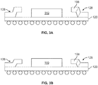
- FIG. 3A-B illustrates example side views of example cavity forming ring stiffeners 128 with different heights.
- the second segment 106 of the cavity forming ring stiffener 128 may be higher than the height of the silicon chip 110.
- the second segment 106 of the cavity forming ring stiffener 128 may be lower than the height of the silicon chip 110.
- the external heat sink 130 may be modified to account for the difference in height between the top of the silicon chip 110 and the height of the second segment 106 of the cavity forming ring stiffener 128.
- FIG. 4 illustrates an example side view of an example external heat sink 130 disposed on the example cavity forming ring stiffener 128 with the second segment 106 of the example cavity forming ring stiffener 128 being higher than the height of the silicon chip 110.
- a portion of the bottom 308 of the external heat sink 130 may be formed with a protrusion 302 over the silicon chip 110.
- the protrusion 302 may be made of the same material or different material than the external heat sink 130.
- a thermal interface material 306 may be disposed between the external heat sink 130 and the silicon chip 110 and between the external heat sink 130 and the second segment 106.
- the protrusion 302 may reduce a thickness of the thermal interface material 306 needed between the silicon chip 110 and the external heat sink 130 compared to the external heat sink 130 without the protrusion 302.
- the thickness of the thermal interface material 306 between the silicon chip 110 and the thickness of the thermal material between the support 106 and the external heat sink 130 may be substantially the same or uniform when the external heat sink is disposed on the second segment 106 and the silicon chip 110.
- the second segment 106 being higher than the top of the silicon chip 110 may also allow for protection of the silicon chip 110 during handling of the FCBGA. Any impacts to the FCBGA will be absorbed by the example cavity forming ring stiffener 128 and not the silicon chip 110.
- a portion of the bottom 308 of the external heat sink 130 may be formed with a recess over the silicon chip 110 (not shown).
- a thermal interface material 306 may be disposed between the external heat sink 130 and the silicon chip 110 and between the external heat sink 130 and the second segment 106.
- the recess on the bottom of the external heat sink 130 may provide space to increase a thickness of the thermal interface material between the silicon chip 110 and the external heat sink 130 compared to the external heat sink 130 without the recess.
- the thickness of the thermal interface material 306 between the silicon chip 110 and the thickness of the thermal material between the support 106 and the external heat sink 130 may be substantially the same or uniform when the external heat sink is disposed on the second segment 106 and the silicon chip 110.
- Other variations are also possible.
- FIG. 5A and 5B illustrate an example side view 500 and an example top view 550 of an example cavity forming ring stiffener 128 with uniform height which is disposed on the substrate 120 of the FCBGA.
- the views may be associated with an x or y dimension which may be the same assuming symmetry of the FCBGA, but in other examples the view may differ depending on dimension.
- the example cavity forming ring stiffener 128 may be a ridged one-piece structure defined by a first segment 502 and second segment 504.
- the first segment 502 may be located along a periphery 506 of the substrate 120.
- the second segment 504 is shown to be at a same height as the top of the silicon chip 110, but may be lower or higher than the top of the silicon chip 110 in other examples.
- the second segment 504 may be oriented substantially parallel to the substrate 120 in a longitudinal direction of the view for length L to form the cavity 112. Additionally, the second segment 504 may be at a uniform height above the substrate 120 from the periphery 506 of the substrate 120 toward a center 508 of the substrate 120 with a slot 510 between the silicon chip 110 and the second segment 504.
- the external heat sink 130 (not shown) may be disposed on the second segment 504 of the cavity forming ring stiffener 128 with a thermal interface material separating the second segment 504 of the cavity forming ring stiffener 128 and the top of the silicon chip 110 from the external heat sink 130.
- An area of the second segment 504 to support the external heat sink 130 may be larger than an area of the second segment 106 because there is no step transition 104 in this example of the cavity forming ring stiffener 128. Further, the first segment 502 may have a thickness greater than the second segment 504 in some examples to increase stability of the cavity forming ring stiffener 128 in supporting the external heat sink 130.
- the cavity forming ring stiffener 128 may be made of a plurality of segments coupled together rather than the one-piece structure.
- FIG. 6 illustrates an example side view of another example cavity forming ring stiffener 128 with uniform height.
- the example cavity forming ring stiffener 128 may be a ridged two-piece structure defined by a first segment 602 and second segment 604 which are affixed at an interface 606.
- the two segments 602, 604 may be affixed by an adhesive connection or mechanical connection, for example, at the interface 606.
- the segment 602 may be a conventional ring stiffener along a periphery 608 of the substrate 120 on top of which is disposed the segment 604 to form the cavity forming ring stiffener 128.
- the segment 604 may be oriented substantially parallel to the substrate 120 in a longitudinal direction of the view for length L.
- the segment 604 may be at a uniform height above the substrate 120 from the periphery 608 of the substrate 120 toward a center 610 of the substrate 120.
- the external heat sink 130 (not shown) may be disposed on the segment 604 of the cavity forming ring stiffener 128, with a thermal interface material separating the silicon chip 110 and the segment 604 from the external heat sink 130.
- the segment 604 may be a support for the external heat sink 130.
- the example cavity forming ring stiffener 128 is described as exposing the top 134 of the silicon chip 110. In other examples, the example cavity forming ring stiffener 128 may further contact the silicon chip 110, e.g., segments 106, 504, or 604 of the example cavity forming ring stiffener 128 contact the silicon chip 110. Contact with the silicon chip 110 may result in the example cavity forming ring stiffener 128 conducting heat from the silicon chip 110 to the substrate 120 of the FCBGA and from the silicon chip 110 to the external heat sink 130 via the thermal interface material 132.
- FIG. 7 is a flow chart 700 of example functions associated with assembly of the example cavity forming ring stiffener 128 and example external heat sink 130 on the FCGBA.
- an example cavity forming ring stiffener 128 is disposed on a substrate 120 of the FCBGA.
- the example cavity forming ring stiffener 128 may expose the top of the silicon chip 110 of the FCBGA.
- the example cavity forming ring stiffener 128 may also define a cavity with respect to substrate 120.
- the example cavity forming ring stiffener 128 may be made of a metal such as copper plated with nickel or with aluminum.
- a thermal interface material is disposed (i) on a segment of the example cavity forming ring stiffener 128 which functions to support an external heat sink 130 and (ii) on a top of the silicon chip 110 of the FCBGA. Examples of this segment of the example cavity forming ring stiffener are shown and described above.
- the thermal interface material 132 may be a thermal grease which has a silicon filler to improve thermal conductivity or other material such as a heat conductive pad which may be a multiple of ten microns thick in some examples.
- the external heat sink 130 is disposed on the thermal interface material 132 to transfer heat from the silicon chip 110 to the external heat sink 130 via the thermal interface material 132.
- the external heat sink 130 may also have plates 124 such as fins to conduct the heat from the silicon chip 110 into the air.
- the FCBGA is surface mounted on a printed circuit board.
- the ball grid array 122 of the substrate 120 may facilitate mounting the FCBGA to the printed circuit board.
Landscapes
- Cooling Or The Like Of Semiconductors Or Solid State Devices (AREA)
Abstract
Description
- This disclosure claims the benefit of priority of
U.S. Provisional Application Serial No. 62/803,204 filed February 8, 2019 - This disclosure relates to a heat sink design for a flip chip ball grid array (FCBGA), namely an external heat sink disposed on a cavity forming ring stiffener which forms a cavity with a substrate of the FCBGA. The cavity forming ring stiffener supports the external heat sink, exposes a top of a silicon chip on the FCBGA, and adds mechanical rigidity to the FCBGA.
- The background description provided herein is for the purpose of generally presenting the context of the disclosure. Work of the presently named inventors, to the extent the work is described in this background section, as well as aspects of the description that may not otherwise qualify as prior art at the time of filing, are neither expressly nor impliedly admitted as prior art against the present disclosure.
- A flip chip ball grid array (FCBGA) is a semiconductor packaging which has a silicon chip disposed on one side of a substrate and a ball grid array disposed on another side of the substrate. The ball grid array enables mounting of the FCBGA on a printed circuit board. The silicon chip generates heat during operation. The heat needs to be dissipated away from the silicon chip to a fluid medium such as air, so that the silicon chip operates at an optimal temperature.
- This disclosure relates to a heat sink design for a flip chip ball grid array (FCBGA), namely an external heat sink which is disposed on a cavity forming ring stiffener which forms a cavity with a substrate of the FCBGA. The cavity forming ring stiffener supports the external heat sink, exposes a top of a silicon chip on a substrate of the FCBGA, and adds mechanical rigidity to the substrate of the FCBGA. Heat is transferred from the silicon chip to the external heat sink for dissipation into a fluid medium such as air via a layer of thermal interface material which separates the silicon chip and the cavity ring stiffener from the external heat sink.
- Aspects of the disclosure provide a flip chip ball grid array (FCBGA) comprising: a substrate having a silicon chip; a cavity forming ring stiffener disposed on the substrate, the cavity forming ring stiffener having a segment which forms a cavity with the substrate and exposes a top of the silicon chip; a thermal interface material disposed on the segment of the cavity forming ring stiffener and the silicon chip; and an external heat sink disposed on the thermal interface material.
- In one example, a segment exposes a portion of the top of the silicon chip. In another example, a height of the segment of the cavity forming ring stiffener is lower or higher than a height of the silicon chip. In yet another example, the segment is a first segment, the cavity forming ring stiffener comprises a second segment disposed along a periphery of the substrate, the second segment transitioning to the first segment by a step transition. In another example, the cavity forming ring stiffener has a uniform height from a periphery of the substrate toward a center of the substrate. In yet another example, the segment is a first segment, the cavity forming ring stiffener comprising a second segment affixed to the first segment. In another example, the second segment is disposed along the periphery of the substrate. In yet another example, the thermal interface material is a thermal grease or a thermally conductive pad. In another example, a height of the segment of the cavity forming ring stiffener is the same as a height of the silicon chip. In yet another example, the segment has a length which exposes a region on the substrate having an integrated circuit or probe pad. In another example, the external heat sink comprises one or more fins perpendicular to the segment of the cavity forming ring stiffener. In yet another example, the external heat sink comprises a recess or protrusion on a bottom of the external heat sink, the recess or the protrusion being over the silicon chip.
- Aspects of the disclosure provide a method comprising: disposing a cavity forming ring stiffener on a substrate of a flip chip ball grid array (FCBGA), the cavity forming ring stiffener having a segment which forms a cavity with the substrate and exposes a top of a silicon chip on the substrate; disposing a thermal interface material on the segment of the cavity forming ring stiffener and the top of the silicon chip; and disposing an external heat sink on the thermal interface material.
- In one example, a segment exposes a portion of the top of the silicon chip. In another example, the method of disposing the cavity forming ring stiffener on the substrate comprises disposing the segment of the cavity forming ring stiffener at a lower or higher height than the silicon chip. In yet another example, a thickness of the thermal interface material is uniform. In another example, the external heat sink comprises a recess or protrusion on a bottom of the external heat sink, the recess or the protrusion being over the silicon chip. In yet another example, the segment is a first segment, the method further comprising affixing the first segment to a second segment disposed along a periphery of the substrate. In another example, the segment is a first segment, the cavity forming ring stiffener comprising a second segment disposed along a periphery of the substrate, the second segment transitioning to the first segment by a step transition. In yet another example, the method further comprises mounting the FCBGA on a printed circuit board.
-
-
FIGs. 1A-1C illustrate various example views of an example flip chip ball grid array (FCBGA) with an example heat sink design. -
FIGs. 2A and 2B illustrate an example top view and an example side view of the example FCBGA having an example cavity forming ring stiffener which does not cover a region on a substrate of the example FCBGA. -
FIG. 3A-B illustrates example side views of example cavity forming ring stiffeners having different heights. -
FIG. 4 illustrates an example side view of an example external heat sink disposed on the example cavity forming ring stiffener with the example cavity forming ring stiffener being higher than the silicon chip. -
FIGs. 5A and5B illustrate various examples view of an example cavity forming ring stiffener with uniform height. -
FIG. 6 illustrates an example side view of another example cavity forming ring stiffener with uniform height. -
FIG. 7 is a flow chart of example functions associated with assembly of the example cavity forming ring stiffener and example external heat sink on a substrate of the FCGBA. - The drawings are for the purpose of illustrating example embodiments, but it is understood that the embodiments are not limited to the arrangements and instrumentality shown in the drawings.
- The description that follows includes example systems, methods, techniques, and program flows that embody aspects of the disclosure. However, it is understood that this disclosure may be practiced without these specific details. For instance, this disclosure relates to an example heat sink design for a flip chip ball grid array (FCBGA), namely an external heat sink and a cavity forming ring stiffener which forms a cavity with a substrate of the FCBGA. Aspects of this disclosure can be applied to semiconductor packaging other than an FBGA and, in other instances, well-known instances, structures, and techniques have not been shown in detail in order not to obfuscate the description.
- An FCBGA arranged with a heat spreader and an external heat sink dissipates heat away from a silicon chip on the FCBGA to a fluid medium such as air, so that the silicon chip operates at an optimal temperature. The heat spreader is arranged over the silicon chip of the FCBGA to entirely cover a top of the silicon chip with supporting ends of the heat spreader coupled to a substrate of the FCBGA. Further, a first layer of thermal interface material such as thermal grease is disposed in between the silicon chip and the heat spreader to transfer heat from the silicon chip to the heat spreader. To dissipate the heat into the air, the external heat sink contacts the heat spreader via a second layer of thermal interface material such as a thermally conductive pad to transfer the heat from the heat spreader to the external heat sink. The external heat sink includes one or more plates such as fins that are oriented perpendicular to the heat spreader to allow the heat to flow into the fins for dissipation into the air.
- The heat flowing from the silicon chip to the heat spreader via the first layer of thermal interface material is a bottleneck to transferring the heat from the silicon chip to the external heat sink. To reduce this bottleneck, a heat sink design is disclosed for the FCBGA. The heat sink design has an external heat sink and a cavity forming ring stiffener which forms a cavity with a substrate of the FCBGA. The cavity forming ring stiffener supports the external heat sink, exposes a silicon chip on a substrate of the FCBGA, and adds mechanical rigidity to a substrate of the FCBGA. The external heat sink may be disposed on the cavity forming ring stiffener and a silicon chip of the FCBGA with a layer of thermal interface material separating the cavity ring stiffener and the silicon chip from the external heat sink. Heat is transferred from the silicon chip to the external heat sink via the layer of the thermal interface material for dissipation into a fluid medium such as air.
- The disclosed heat sink structure eliminates the layer of thermal interface material between a heat spreader and silicon chip needed to manage heat on the FCBGA and reduces a junction to case (e.g., silicon chip to external heat sink) thermal resistance. The heat from the silicon chip is not transferred from the silicon chip to the heat spreader via the first layer of thermal interface material and then from the heat spreader to the external heat sink via the second layer of thermal interface material. Instead the heat is transferred from the silicon chip to the external heat sink via a single layer of thermal interface material. The disclosed external heat sink for the FCBGA provides other advantages as well.
-
FIGs. 1A-1C illustrate various example views of an example flip chip ball grid array (FCBGA) with an example heat sink design.FIG. 1A and FIG. 1B show aside view 100 and atop view 150, respectively, of a cavity formingring stiffener 128 of the FCBGA. Further,FIG. 1C shows anexternal heat sink 130 of the FCBGA which is disposed on the cavity formingring stiffener 128. The views associated withFIG. 1A and FIG. 1C may be associated with an x or y dimension which may be the same assuming symmetry of the FCBGA, but in other examples views may differ depending on dimension. Similar components in the views are labeled with similar reference numbers. - The FCBGA has a
silicon chip 110 disposed on one side of asubstrate 120 and aball grid array 122 disposed on other side of thesubstrate 120. Thesilicon chip 110 may be an integrated circuit disposed on thesubstrate 120 using a controlled collapse chip connection. The controlled collapse chip connection, or its abbreviation, C4, is a method for interconnecting semiconductor devices such as thesilicon chip 110 to circuitry such as thesubstrate 120 with solder bumps that have been deposited onto chip pads. Theball grid array 122 which is disposed on other side of thesubstrate 120 is a type of surface-mount packaging used for integrated circuits. Theball grid array 122 allows for surface mounting the FCBGA to a printed circuit board (not shown). - The
silicon chip 110 may generate heat during operation. So that the silicon chip operates at an optimal temperature, theexternal heat sink 130 may be disposed on the cavity formingring stiffener 128 and thesilicon chip 110. Theexternal heat sink 130 may transfer the heat generated by thesilicon chip 110 during operation to a fluid medium such as air for dissipation away from thesilicon chip 110. - The cavity forming
ring stiffener 128 may be a rigid one-piece structure made of a metal such as copper with nickel plating or with aluminum. The cavity formingring stiffener 128 may be defined by afirst segment 102, astep transition 104 or downstep, and asecond segment 106, each of which are separated by dotted lines. Further, thefirst segment 102, thestep transition 104 or downstep, and thesecond segment 106 are shown for one side of the cavity formingring stiffener 128 for ease of illustration but both sides of the cavity formingring stiffener 128 may be composed similarly. Thefirst segment 102, thestep transition 104 or downstep, and thesecond segment 106 may each have a thickness ranging from 0.3 to 4 mm in examples. At least thesecond segment 106 and thesubstrate 120 may form acavity 112 and in examples thefirst segment 102 may be lower than thesecond segment 106. Thefirst segment 102 may be disposed along a periphery of thesubstrate 120 to support the cavity forming ring stiffener and thesecond segment 106 may be oriented substantially parallel to thesubstrate 120 with a height H. Thestep transition 104 may facilitate a transition from thefirst segment 102 to thesecond segment 106 which are at different heights. Thesecond segment 106 with length L may expose the top 134 of thesilicon chip 110 as shown in thetop view 150. The exposure may be that thesegment 106 covers a portion of the top 134 or does not cover the top 134 at all. In examples, the length L of thesecond segment 106 may define aslot 108 between thesilicon chip 110 and thesecond segment 106 in thetop view 150. - The cavity forming
ring stiffener 128 further supports theexternal heat sink 130 and adds mechanical rigidity to prevent warpage of thesubstrate 120. The rigidity is increased compared to a ring structure which does not form thecavity 112. Theexternal heat sink 130 shown inFIG. 1C along with the cavity formingring stiffener 128 may also be made of various metals such as copper with nickel plating or aluminum. Theexternal heat sink 130 may be disposed on thesecond segment 106 of the cavity formingring stiffener 128 and ontop 134 of thesilicon chip 110 and separated by a layer ofthermal interface material 132. In examples, the layer of thethermal interface material 132 may have a uniform thickness. Thethermal interface material 132 may be a material with a thermal resistance which facilitates conduction of heat, such as a thermal grease with a silicon-based filler or a thermally conductive pad such as a graphite pad with a thickness in a range of tens of microns. Thermal grease (also called heat paste, heat sink compound, heat sink paste, thermal compound, thermal gel, thermal interface material, or thermal paste) is a thermally conductive (but usually electrically insulating) compound. A role of thermal grease may be to eliminate air gaps or spaces (which act as thermal insulation) from an interface area in order to maximize heat transfer and dissipation. Thethermal interface material 132 may conduct the heat from thesilicon chip 110 which is exposed by the cavity formingring stiffener 128 to theexternal heat sink 130. To dissipate the heat into the air, theexternal heat sink 130 may include one ormore plates 124 on a top of theexternal heat sink 130 such as fins. In some examples, the fins may be oriented perpendicular to thesecond segment 106 of the cavity formingring stiffener 128. The heat flows from thesilicon chip 110, through thethermal interface material 132, and theplates 124 of theexternal heat sink 130 for dissipation into the air. - The
second segment 106 of the cavity formingring stiffener 128 may have the length L which exposes the top 134 of thesilicon chip 110 in different amounts. In some examples, the length L of thesecond segment 106 of the cavity formingring stiffener 128 may be sized so that thesecond segment 106 does not cover the top 134 of thesilicon chip 110 and does not cover a region on thesubstrate 120 adjacent to thesilicon chip 110. The region is not covered, allowing for access to the region from above so long as theexternal heat sink 130 andthermal interface material 132 is not disposed on the cavity formingring stiffener 128. -
FIGs. 2A and 2B illustrate anexample side view 200 and an exampletop view 250 of the example FCBGA having the example cavity formingring stiffener 128 with thesecond segment 106 which does not cover aregion 202 on thesubstrate 120 of the example FCBGA. In examples, theregion 202 may have a probe pad coupled to thesilicon chip 110 to probe thesilicon chip 110 and/or integrated circuitry. Thesecond segment 106 of the cavity formingring stiffener 128 may have a length L so as to not extend above theregion 202 to cover theregion 202. Further, thesecond segment 106 may not cover the top of thesilicon chip 110. Theslot 108 between thesilicon chip 110 and thesecond segment 106 may take different shapes. The shape that is shown in thetop view 250 is a circle indicating that the length L may vary along the x or y dimension around thesilicon chip 110, but the shape may take other forms including a rectangle or oval. Theslot 108 may allow for access to theregion 202 from above when the external heat sink 130 (not shown) is not disposed on the cavity formingring stiffener 128. - In the examples above, a height of the cavity forming
ring stiffener 128 and a height of the top of thesilicon chip 110 may be the same, e.g., thesecond segment 106 and the top of thesilicon chip 110 are in a same plane. In other examples, thesecond segment 106 of the cavity formingring stiffener 128 may be below or above the top of thesilicon chip 110. -
FIG. 3A-B illustrates example side views of example cavity formingring stiffeners 128 with different heights. InFIG. 3A , thesecond segment 106 of the cavity formingring stiffener 128 may be higher than the height of thesilicon chip 110. InFIG. 3B , thesecond segment 106 of the cavity formingring stiffener 128 may be lower than the height of thesilicon chip 110. Theexternal heat sink 130 may be modified to account for the difference in height between the top of thesilicon chip 110 and the height of thesecond segment 106 of the cavity formingring stiffener 128. -
FIG. 4 illustrates an example side view of an exampleexternal heat sink 130 disposed on the example cavity formingring stiffener 128 with thesecond segment 106 of the example cavity formingring stiffener 128 being higher than the height of thesilicon chip 110. A portion of the bottom 308 of theexternal heat sink 130 may be formed with aprotrusion 302 over thesilicon chip 110. Theprotrusion 302 may be made of the same material or different material than theexternal heat sink 130. Athermal interface material 306 may be disposed between theexternal heat sink 130 and thesilicon chip 110 and between theexternal heat sink 130 and thesecond segment 106. Theprotrusion 302 may reduce a thickness of thethermal interface material 306 needed between thesilicon chip 110 and theexternal heat sink 130 compared to theexternal heat sink 130 without theprotrusion 302. For example, the thickness of thethermal interface material 306 between thesilicon chip 110 and the thickness of the thermal material between thesupport 106 and theexternal heat sink 130 may be substantially the same or uniform when the external heat sink is disposed on thesecond segment 106 and thesilicon chip 110. Thesecond segment 106 being higher than the top of thesilicon chip 110 may also allow for protection of thesilicon chip 110 during handling of the FCBGA. Any impacts to the FCBGA will be absorbed by the example cavity formingring stiffener 128 and not thesilicon chip 110. If thesecond segment 106 of the example cavity formingring stiffener 128 is lower than the height of thesilicon chip 110, a portion of the bottom 308 of theexternal heat sink 130 may be formed with a recess over the silicon chip 110 (not shown). Athermal interface material 306 may be disposed between theexternal heat sink 130 and thesilicon chip 110 and between theexternal heat sink 130 and thesecond segment 106. The recess on the bottom of theexternal heat sink 130 may provide space to increase a thickness of the thermal interface material between thesilicon chip 110 and theexternal heat sink 130 compared to theexternal heat sink 130 without the recess. For example, the thickness of thethermal interface material 306 between thesilicon chip 110 and the thickness of the thermal material between thesupport 106 and theexternal heat sink 130 may be substantially the same or uniform when the external heat sink is disposed on thesecond segment 106 and thesilicon chip 110. Other variations are also possible. -
FIG. 5A and5B illustrate anexample side view 500 and an exampletop view 550 of an example cavity formingring stiffener 128 with uniform height which is disposed on thesubstrate 120 of the FCBGA. The views may be associated with an x or y dimension which may be the same assuming symmetry of the FCBGA, but in other examples the view may differ depending on dimension. The example cavity formingring stiffener 128 may be a ridged one-piece structure defined by afirst segment 502 andsecond segment 504. Thefirst segment 502 may be located along aperiphery 506 of thesubstrate 120. Thesecond segment 504 is shown to be at a same height as the top of thesilicon chip 110, but may be lower or higher than the top of thesilicon chip 110 in other examples. Thesecond segment 504 may be oriented substantially parallel to thesubstrate 120 in a longitudinal direction of the view for length L to form thecavity 112. Additionally, thesecond segment 504 may be at a uniform height above thesubstrate 120 from theperiphery 506 of thesubstrate 120 toward acenter 508 of thesubstrate 120 with aslot 510 between thesilicon chip 110 and thesecond segment 504. In examples, the external heat sink 130 (not shown) may be disposed on thesecond segment 504 of the cavity formingring stiffener 128 with a thermal interface material separating thesecond segment 504 of the cavity formingring stiffener 128 and the top of thesilicon chip 110 from theexternal heat sink 130. An area of thesecond segment 504 to support theexternal heat sink 130 may be larger than an area of thesecond segment 106 because there is nostep transition 104 in this example of the cavity formingring stiffener 128. Further, thefirst segment 502 may have a thickness greater than thesecond segment 504 in some examples to increase stability of the cavity formingring stiffener 128 in supporting theexternal heat sink 130. - In some examples, the cavity forming
ring stiffener 128 may be made of a plurality of segments coupled together rather than the one-piece structure. -
FIG. 6 illustrates an example side view of another example cavity formingring stiffener 128 with uniform height. The example cavity formingring stiffener 128 may be a ridged two-piece structure defined by afirst segment 602 andsecond segment 604 which are affixed at aninterface 606. The twosegments interface 606. Thesegment 602 may be a conventional ring stiffener along aperiphery 608 of thesubstrate 120 on top of which is disposed thesegment 604 to form the cavity formingring stiffener 128. Thesegment 604 may be oriented substantially parallel to thesubstrate 120 in a longitudinal direction of the view for length L. Further, thesegment 604 may be at a uniform height above thesubstrate 120 from theperiphery 608 of thesubstrate 120 toward acenter 610 of thesubstrate 120. In examples, the external heat sink 130 (not shown) may be disposed on thesegment 604 of the cavity formingring stiffener 128, with a thermal interface material separating thesilicon chip 110 and thesegment 604 from theexternal heat sink 130. Thesegment 604 may be a support for theexternal heat sink 130. - In the above examples, the example cavity forming
ring stiffener 128 is described as exposing the top 134 of thesilicon chip 110. In other examples, the example cavity formingring stiffener 128 may further contact thesilicon chip 110, e.g.,segments ring stiffener 128 contact thesilicon chip 110. Contact with thesilicon chip 110 may result in the example cavity formingring stiffener 128 conducting heat from thesilicon chip 110 to thesubstrate 120 of the FCBGA and from thesilicon chip 110 to theexternal heat sink 130 via thethermal interface material 132. -
FIG. 7 is aflow chart 700 of example functions associated with assembly of the example cavity formingring stiffener 128 and exampleexternal heat sink 130 on the FCGBA. - At 702, an example cavity forming
ring stiffener 128 is disposed on asubstrate 120 of the FCBGA. The example cavity formingring stiffener 128 may expose the top of thesilicon chip 110 of the FCBGA. The example cavity formingring stiffener 128 may also define a cavity with respect tosubstrate 120. The example cavity formingring stiffener 128 may be made of a metal such as copper plated with nickel or with aluminum. - At 704, a thermal interface material is disposed (i) on a segment of the example cavity forming
ring stiffener 128 which functions to support anexternal heat sink 130 and (ii) on a top of thesilicon chip 110 of the FCBGA. Examples of this segment of the example cavity forming ring stiffener are shown and described above. Thethermal interface material 132 may be a thermal grease which has a silicon filler to improve thermal conductivity or other material such as a heat conductive pad which may be a multiple of ten microns thick in some examples. - At 706, the
external heat sink 130 is disposed on thethermal interface material 132 to transfer heat from thesilicon chip 110 to theexternal heat sink 130 via thethermal interface material 132. Theexternal heat sink 130 may also haveplates 124 such as fins to conduct the heat from thesilicon chip 110 into the air. - At 708, the FCBGA is surface mounted on a printed circuit board. In examples, the
ball grid array 122 of thesubstrate 120 may facilitate mounting the FCBGA to the printed circuit board. - Use of the phrase "at least one of" preceding a list with the conjunction "and" should not be treated as an exclusive list and should not be construed as a list of categories with one item from each category, unless specifically stated otherwise. A clause that recites "at least one of A, B, and C" can be infringed with only one of the listed items, multiple of the listed items, and one or more of the items in the list and another item not listed.
- While aspects of the present disclosure have been described in conjunction with the specific embodiments thereof that are proposed as examples, alternatives, modifications, and variations to the examples may be made. Accordingly, embodiments as set forth herein are intended to be illustrative and not limiting. There are changes that may be made without departing from the scope of the claims set forth below.
- The following is a list of further preferred embodiments of the invention:
- Embodiment 1: A flip chip ball grid array (FCBGA) comprising:
- a substrate having a silicon chip;
- a cavity forming ring stiffener disposed on the substrate, the cavity forming ring stiffener having a segment which forms a cavity with the substrate and exposes a top of the silicon chip;
- a thermal interface material disposed on the segment of the cavity forming ring stiffener and the silicon chip; and
- an external heat sink disposed on the thermal interface material.
- Embodiment 2: The FCBGA of embodiment 1, wherein a segment exposes a portion of the top of the silicon chip.
- Embodiment 3: The FCBGA of embodiment 1, wherein a height of the segment of the cavity forming ring stiffener is lower or higher than a height of the silicon chip.
- Embodiment 4: The FCBGA of embodiment 1, wherein the segment is a first segment, the cavity forming ring stiffener comprising a second segment disposed along a periphery of the substrate, the second segment transitioning to the first segment by a step transition.
- Embodiment 5: The FCBGA of embodiment 1, wherein the cavity forming ring stiffener has a uniform height from a periphery of the substrate toward a center of the substrate.
- Embodiment 6: The FCBGA of embodiment 5, wherein the segment is a first segment, the cavity forming ring stiffener comprising a second segment affixed to the first segment.
- Embodiment 7: The FCBGA of embodiment 6, wherein the second segment is disposed along the periphery of the substrate.
- Embodiment 8: The FCBGA of embodiment 1, wherein the thermal interface material is a thermal grease or a thermally conductive pad.
- Embodiment 9: The FCBGA of embodiment 1, wherein a height of the segment of the cavity forming ring stiffener is the same as a height of the silicon chip.
- Embodiment 10: The FCBGA of embodiment 1, wherein the segment has a length which exposes a region on the substrate having an integrated circuit or probe pad.
- Embodiment 11: The FCBGA of embodiment 1, wherein the external heat sink comprises one or more fins perpendicular to the segment of the cavity forming ring stiffener.
- Embodiment 12: The FCBGA of embodiment 1, wherein the external heat sink comprises a recess or protrusion on a bottom of the external heat sink, the recess or the protrusion being over the silicon chip.
- Embodiment 13: A method comprising:
- disposing a cavity forming ring stiffener on a substrate of a flip chip ball grid array (FCBGA), the cavity forming ring stiffener having a segment which forms a cavity with the substrate and exposes a top of a silicon chip on the substrate;
- disposing a thermal interface material on the segment of the cavity forming ring stiffener and the top of the silicon chip; and
- disposing an external heat sink on the thermal interface material.
- Embodiment 14: The method of embodiment 13, wherein a segment exposes a portion of the top of the silicon chip.
- Embodiment 15: The method of embodiment 13, wherein disposing the cavity forming ring stiffener on the substrate comprises disposing the segment of the cavity forming ring stiffener at a lower or higher height than the silicon chip.
- Embodiment 16: The method of embodiment 13, wherein a thickness of the thermal interface material is uniform.
- Embodiment 17: The method of embodiment 13, wherein the external heat sink comprises a recess or protrusion on a bottom of the external heat sink, the recess or the protrusion being over the silicon chip.
- Embodiment 18: The method of embodiment 13, wherein the segment is a first segment, the method further comprising affixing the first segment to a second segment disposed along a periphery of the substrate.
- Embodiment 19: The method of embodiment 13, wherein the segment is a first segment, the cavity forming ring stiffener comprising a second segment disposed along a periphery of the substrate, the second segment transitioning to the first segment by a step transition.
- Embodiment 20: The method of embodiment 13, further comprising mounting the FCBGA on a printed circuit board.
Claims (15)
- A flip chip ball grid array (FCBGA) comprising:a substrate having a silicon chip;a cavity forming ring stiffener disposed on the substrate, the cavity forming ring stiffener having a segment which forms a cavity with the substrate and exposes a top of the silicon chip;a thermal interface material disposed on the segment of the cavity forming ring stiffener and the silicon chip; andan external heat sink disposed on the thermal interface material.
- The FCBGA of claim 1, wherein a segment exposes a portion of the top of the silicon chip.
- The FCBGA of claim 1, wherein a height of the segment of the cavity forming ring stiffener is lower or higher than a height of the silicon chip.
- The FCBGA of one of claims 1 to 3, wherein the segment is a first segment, the cavity forming ring stiffener comprising a second segment disposed along a periphery of the substrate, the second segment transitioning to the first segment by a step transition.
- The FCBGA of one of claims 1 to 4, wherein the cavity forming ring stiffener has a uniform height from a periphery of the substrate toward a center of the substrate.
- The FCBGA of claim 5, wherein the segment is a first segment, the cavity forming ring stiffener comprising a second segment affixed to the first segment.
- The FCBGA of claim 6, wherein the second segment is disposed along the periphery of the substrate.
- The FCBGA of one of claims 1 to 7, wherein the thermal interface material is a thermal grease or a thermally conductive pad.
- The FCBGA of one of claims 1 to 8, wherein a height of the segment of the cavity forming ring stiffener is the same as a height of the silicon chip.
- The FCBGA of one of claims 1 to 9, wherein the segment has a length which exposes a region on the substrate having an integrated circuit or probe pad.
- The FCBGA of one of claims 1 to 10, wherein the external heat sink comprises one or more fins perpendicular to the segment of the cavity forming ring stiffener.
- The FCBGA of one of claims 1 to 11, wherein the external heat sink comprises a recess or protrusion on a bottom of the external heat sink, the recess or the protrusion being over the silicon chip.
- A method comprising:disposing a cavity forming ring stiffener on a substrate of a flip chip ball grid array (FCBGA), the cavity forming ring stiffener having a segment which forms a cavity with the substrate and exposes a top of a silicon chip on the substrate;disposing a thermal interface material on the segment of the cavity forming ring stiffener and the top of the silicon chip; anddisposing an external heat sink on the thermal interface material.
- The method of claim 13, wherein a segment exposes a portion of the top of the silicon chip.
- The method of claim 13, wherein disposing the cavity forming ring stiffener on the substrate comprises disposing the segment of the cavity forming ring stiffener at a lower or higher height than the silicon chip; or
wherein a thickness of the thermal interface material is uniform; or
wherein the external heat sink comprises a recess or protrusion on a bottom of the external heat sink, the recess or the protrusion being over the silicon chip.
wherein the segment is a first segment, the method further comprising affixing the first segment to a second segment disposed along a periphery of the substrate; or
wherein the segment is a first segment, the cavity forming ring stiffener comprising a second segment disposed along a periphery of the substrate, the second segment transitioning to the first segment by a step transition; or
further comprising mounting the FCBGA on a printed circuit board.
Applications Claiming Priority (1)
| Application Number | Priority Date | Filing Date | Title |
|---|---|---|---|
| US201962803204P | 2019-02-08 | 2019-02-08 |
Publications (2)
| Publication Number | Publication Date |
|---|---|
| EP3693991A1 true EP3693991A1 (en) | 2020-08-12 |
| EP3693991B1 EP3693991B1 (en) | 2024-04-03 |
Family
ID=69570514
Family Applications (1)
| Application Number | Title | Priority Date | Filing Date |
|---|---|---|---|
| EP20156122.2A Active EP3693991B1 (en) | 2019-02-08 | 2020-02-07 | Heat sink design for flip chip ball grid array |
Country Status (4)
| Country | Link |
|---|---|
| US (1) | US11282762B2 (en) |
| EP (1) | EP3693991B1 (en) |
| KR (1) | KR102754126B1 (en) |
| CN (1) | CN111554643B (en) |
Families Citing this family (5)
| Publication number | Priority date | Publication date | Assignee | Title |
|---|---|---|---|---|
| WO2022067589A1 (en) * | 2020-09-29 | 2022-04-07 | 华为技术有限公司 | Chip package and electronic device |
| US11823991B2 (en) * | 2021-03-26 | 2023-11-21 | Taiwan Semiconductor Manufacturing Company, Ltd. | Frames stacked on substrate encircling devices and manufacturing method thereof |
| KR20230025132A (en) | 2021-08-13 | 2023-02-21 | 삼성전자주식회사 | Semiconductor package including stiffener |
| US11830785B2 (en) * | 2021-10-06 | 2023-11-28 | STATS ChipPAC Pte. Ltd. | Package with windowed heat spreader |
| CN114038815A (en) * | 2021-10-15 | 2022-02-11 | 飞腾信息技术有限公司 | Flip chip ball grid array packaging structure and chip heat dissipation performance optimization method |
Citations (5)
| Publication number | Priority date | Publication date | Assignee | Title |
|---|---|---|---|---|
| US6724080B1 (en) * | 2002-12-20 | 2004-04-20 | Altera Corporation | Heat sink with elevated heat spreader lid |
| US20090283902A1 (en) * | 2008-05-13 | 2009-11-19 | Raschid Jose Bezama | Semiconductor Package Structures Having Liquid Coolers Integrated with First Level Chip Package Modules |
| WO2013089780A1 (en) * | 2011-12-16 | 2013-06-20 | Intel Corporation | Package for a microelectronic die, microelectronic assembly containing same, microelectronic system, and method of reducing die stress in a microelectronic package |
| US20140002989A1 (en) * | 2012-06-27 | 2014-01-02 | Sandeep Ahuja | Integrated heat spreader that maximizes heat transfer from a multi-chip package |
| EP3373331A1 (en) * | 2017-03-08 | 2018-09-12 | MediaTek Inc. | Semiconductor package with stiffener ring |
Family Cites Families (15)
| Publication number | Priority date | Publication date | Assignee | Title |
|---|---|---|---|---|
| JPH06252301A (en) * | 1993-02-24 | 1994-09-09 | Hitachi Ltd | Electronic device |
| US5986340A (en) * | 1996-05-02 | 1999-11-16 | National Semiconductor Corporation | Ball grid array package with enhanced thermal and electrical characteristics and electronic device incorporating same |
| JP2005136302A (en) * | 2003-10-31 | 2005-05-26 | Renesas Technology Corp | Manufacturing method of semiconductor integrated circuit device |
| JP2006222406A (en) * | 2004-08-06 | 2006-08-24 | Denso Corp | Semiconductor device |
| TWI249232B (en) * | 2004-10-20 | 2006-02-11 | Siliconware Precision Industries Co Ltd | Heat dissipating package structure and method for fabricating the same |
| TWI246759B (en) * | 2004-11-16 | 2006-01-01 | Siliconware Precision Industries Co Ltd | Heat dissipating package structure and fabrication method thereof |
| JP2007273233A (en) * | 2006-03-31 | 2007-10-18 | Fujitsu Ltd | Socket, circuit component having socket, and information processing apparatus including circuit component |
| TW200802629A (en) * | 2006-06-12 | 2008-01-01 | Siliconware Precision Industries Co Ltd | Heat sink package structure and method for fabricating the same |
| TWI343103B (en) * | 2007-06-13 | 2011-06-01 | Siliconware Precision Industries Co Ltd | Heat dissipation type package structure and fabrication method thereof |
| US8216887B2 (en) * | 2009-05-04 | 2012-07-10 | Advanced Micro Devices, Inc. | Semiconductor chip package with stiffener frame and configured lid |
| US8796822B2 (en) * | 2011-10-07 | 2014-08-05 | Freescale Semiconductor, Inc. | Stacked semiconductor devices |
| US9142481B2 (en) * | 2012-06-05 | 2015-09-22 | Stats Chippac Ltd. | Integrated circuit packaging system with heatsink cap and method of manufacture thereof |
| US9281254B2 (en) * | 2014-02-13 | 2016-03-08 | Taiwan Semiconductor Manufacturing Company, Ltd. | Methods of forming integrated circuit package |
| CN103871985A (en) * | 2014-03-03 | 2014-06-18 | 江苏长电科技股份有限公司 | Semiconductor packaging structure |
| US20180235069A1 (en) * | 2016-12-16 | 2018-08-16 | Hamilton Sundstrand Corporation | Pressure limiting heat sink |
-
2020
- 2020-02-07 US US16/784,869 patent/US11282762B2/en active Active
- 2020-02-07 KR KR1020200015064A patent/KR102754126B1/en active Active
- 2020-02-07 EP EP20156122.2A patent/EP3693991B1/en active Active
- 2020-02-10 CN CN202010085306.7A patent/CN111554643B/en active Active
Patent Citations (5)
| Publication number | Priority date | Publication date | Assignee | Title |
|---|---|---|---|---|
| US6724080B1 (en) * | 2002-12-20 | 2004-04-20 | Altera Corporation | Heat sink with elevated heat spreader lid |
| US20090283902A1 (en) * | 2008-05-13 | 2009-11-19 | Raschid Jose Bezama | Semiconductor Package Structures Having Liquid Coolers Integrated with First Level Chip Package Modules |
| WO2013089780A1 (en) * | 2011-12-16 | 2013-06-20 | Intel Corporation | Package for a microelectronic die, microelectronic assembly containing same, microelectronic system, and method of reducing die stress in a microelectronic package |
| US20140002989A1 (en) * | 2012-06-27 | 2014-01-02 | Sandeep Ahuja | Integrated heat spreader that maximizes heat transfer from a multi-chip package |
| EP3373331A1 (en) * | 2017-03-08 | 2018-09-12 | MediaTek Inc. | Semiconductor package with stiffener ring |
Also Published As
| Publication number | Publication date |
|---|---|
| KR102754126B1 (en) | 2025-01-14 |
| CN111554643A (en) | 2020-08-18 |
| KR20200097659A (en) | 2020-08-19 |
| US20200258807A1 (en) | 2020-08-13 |
| EP3693991B1 (en) | 2024-04-03 |
| US11282762B2 (en) | 2022-03-22 |
| CN111554643B (en) | 2025-06-13 |
Similar Documents
| Publication | Publication Date | Title |
|---|---|---|
| US11282762B2 (en) | Heat sink design for flip chip ball grid array | |
| CN213752684U (en) | Stacked silicon package assembly with vertical thermal management | |
| EP2789009B1 (en) | Design of a heat dissipation structure for an integrated circuit (ic) chip | |
| US5513070A (en) | Dissipation of heat through keyboard using a heat pipe | |
| US5430611A (en) | Spring-biased heat sink assembly for a plurality of integrated circuits on a substrate | |
| US5396403A (en) | Heat sink assembly with thermally-conductive plate for a plurality of integrated circuits on a substrate | |
| US6462410B1 (en) | Integrated circuit component temperature gradient reducer | |
| US5095404A (en) | Arrangement for mounting and cooling high density tab IC chips | |
| US6188578B1 (en) | Integrated circuit package with multiple heat dissipation paths | |
| US8304922B2 (en) | Semiconductor package system with thermal die bonding | |
| US6657864B1 (en) | High density thermal solution for direct attach modules | |
| EP0883192A2 (en) | Grooved semiconductor die for flip-chip sink attachment | |
| US7561425B2 (en) | Encapsulated multi-phase electronics heat-sink | |
| EP3695438B1 (en) | Heat sink, integrated circuit chip and circuit board | |
| US11587887B2 (en) | Semiconductor device and manufacturing method thereof | |
| US7049695B1 (en) | Method and device for heat dissipation in semiconductor modules | |
| JPH10247703A (en) | Ball grid array package and printed board | |
| EP4456128A1 (en) | Thermal management systems and methods for semiconductor devices | |
| JPH04291750A (en) | Head radiating fin and semiconductor integrated circuit device | |
| JPH07112029B2 (en) | Electronic component cooling device | |
| CN120809692B (en) | A heat dissipation chip packaging structure, a heat dissipation packaging device, and an electronic device. | |
| US20250379120A1 (en) | Semiconductor package including heat transfer member | |
| US20260136933A1 (en) | Microchip package with integrated cold plate | |
| US20250309040A1 (en) | Electronic package and manufacturing method thereof | |
| US20260123410A1 (en) | Lid Design and Process for Dispensable Liquid Metal Thermal Interface Material |
Legal Events
| Date | Code | Title | Description |
|---|---|---|---|
| PUAI | Public reference made under article 153(3) epc to a published international application that has entered the european phase |
Free format text: ORIGINAL CODE: 0009012 |
|
| STAA | Information on the status of an ep patent application or granted ep patent |
Free format text: STATUS: THE APPLICATION HAS BEEN PUBLISHED |
|
| AK | Designated contracting states |
Kind code of ref document: A1 Designated state(s): AL AT BE BG CH CY CZ DE DK EE ES FI FR GB GR HR HU IE IS IT LI LT LU LV MC MK MT NL NO PL PT RO RS SE SI SK SM TR |
|
| AX | Request for extension of the european patent |
Extension state: BA ME |
|
| STAA | Information on the status of an ep patent application or granted ep patent |
Free format text: STATUS: REQUEST FOR EXAMINATION WAS MADE |
|
| 17P | Request for examination filed |
Effective date: 20200806 |
|
| RBV | Designated contracting states (corrected) |
Designated state(s): AL AT BE BG CH CY CZ DE DK EE ES FI FR GB GR HR HU IE IS IT LI LT LU LV MC MK MT NL NO PL PT RO RS SE SI SK SM TR |
|
| STAA | Information on the status of an ep patent application or granted ep patent |
Free format text: STATUS: EXAMINATION IS IN PROGRESS |
|
| 17Q | First examination report despatched |
Effective date: 20210824 |
|
| P01 | Opt-out of the competence of the unified patent court (upc) registered |
Effective date: 20230509 |
|
| GRAP | Despatch of communication of intention to grant a patent |
Free format text: ORIGINAL CODE: EPIDOSNIGR1 |
|
| STAA | Information on the status of an ep patent application or granted ep patent |
Free format text: STATUS: GRANT OF PATENT IS INTENDED |
|
| RIC1 | Information provided on ipc code assigned before grant |
Ipc: H01L 23/42 20060101ALI20230731BHEP Ipc: H01L 23/13 20060101ALI20230731BHEP Ipc: H01L 23/16 20060101ALI20230731BHEP Ipc: H01L 23/433 20060101ALI20230731BHEP Ipc: H01L 23/498 20060101ALI20230731BHEP Ipc: H01L 23/373 20060101ALI20230731BHEP Ipc: H01L 23/367 20060101AFI20230731BHEP |
|
| INTG | Intention to grant announced |
Effective date: 20230829 |
|
| GRAS | Grant fee paid |
Free format text: ORIGINAL CODE: EPIDOSNIGR3 |
|
| GRAA | (expected) grant |
Free format text: ORIGINAL CODE: 0009210 |
|
| STAA | Information on the status of an ep patent application or granted ep patent |
Free format text: STATUS: THE PATENT HAS BEEN GRANTED |
|
| AK | Designated contracting states |
Kind code of ref document: B1 Designated state(s): AL AT BE BG CH CY CZ DE DK EE ES FI FR GB GR HR HU IE IS IT LI LT LU LV MC MK MT NL NO PL PT RO RS SE SI SK SM TR |
|
| REG | Reference to a national code |
Ref country code: CH Ref legal event code: EP |
|
| REG | Reference to a national code |
Ref country code: DE Ref legal event code: R096 Ref document number: 602020028159 Country of ref document: DE |
|
| REG | Reference to a national code |
Ref country code: IE Ref legal event code: FG4D |
|
| REG | Reference to a national code |
Ref country code: LT Ref legal event code: MG9D |
|
| REG | Reference to a national code |
Ref country code: NL Ref legal event code: MP Effective date: 20240403 |
|
| REG | Reference to a national code |
Ref country code: AT Ref legal event code: MK05 Ref document number: 1673355 Country of ref document: AT Kind code of ref document: T Effective date: 20240403 |
|
| PG25 | Lapsed in a contracting state [announced via postgrant information from national office to epo] |
Ref country code: NL Free format text: LAPSE BECAUSE OF FAILURE TO SUBMIT A TRANSLATION OF THE DESCRIPTION OR TO PAY THE FEE WITHIN THE PRESCRIBED TIME-LIMIT Effective date: 20240403 |
|
| PG25 | Lapsed in a contracting state [announced via postgrant information from national office to epo] |
Ref country code: NL Free format text: LAPSE BECAUSE OF FAILURE TO SUBMIT A TRANSLATION OF THE DESCRIPTION OR TO PAY THE FEE WITHIN THE PRESCRIBED TIME-LIMIT Effective date: 20240403 |
|
| PG25 | Lapsed in a contracting state [announced via postgrant information from national office to epo] |
Ref country code: IS Free format text: LAPSE BECAUSE OF FAILURE TO SUBMIT A TRANSLATION OF THE DESCRIPTION OR TO PAY THE FEE WITHIN THE PRESCRIBED TIME-LIMIT Effective date: 20240803 |
|
| PG25 | Lapsed in a contracting state [announced via postgrant information from national office to epo] |
Ref country code: BG Free format text: LAPSE BECAUSE OF FAILURE TO SUBMIT A TRANSLATION OF THE DESCRIPTION OR TO PAY THE FEE WITHIN THE PRESCRIBED TIME-LIMIT Effective date: 20240403 |
|
| PG25 | Lapsed in a contracting state [announced via postgrant information from national office to epo] |
Ref country code: HR Free format text: LAPSE BECAUSE OF FAILURE TO SUBMIT A TRANSLATION OF THE DESCRIPTION OR TO PAY THE FEE WITHIN THE PRESCRIBED TIME-LIMIT Effective date: 20240403 Ref country code: FI Free format text: LAPSE BECAUSE OF FAILURE TO SUBMIT A TRANSLATION OF THE DESCRIPTION OR TO PAY THE FEE WITHIN THE PRESCRIBED TIME-LIMIT Effective date: 20240403 |
|
| PG25 | Lapsed in a contracting state [announced via postgrant information from national office to epo] |
Ref country code: GR Free format text: LAPSE BECAUSE OF FAILURE TO SUBMIT A TRANSLATION OF THE DESCRIPTION OR TO PAY THE FEE WITHIN THE PRESCRIBED TIME-LIMIT Effective date: 20240704 |
|
| PG25 | Lapsed in a contracting state [announced via postgrant information from national office to epo] |
Ref country code: PT Free format text: LAPSE BECAUSE OF FAILURE TO SUBMIT A TRANSLATION OF THE DESCRIPTION OR TO PAY THE FEE WITHIN THE PRESCRIBED TIME-LIMIT Effective date: 20240805 |
|
| PG25 | Lapsed in a contracting state [announced via postgrant information from national office to epo] |
Ref country code: ES Free format text: LAPSE BECAUSE OF FAILURE TO SUBMIT A TRANSLATION OF THE DESCRIPTION OR TO PAY THE FEE WITHIN THE PRESCRIBED TIME-LIMIT Effective date: 20240403 |
|
| PG25 | Lapsed in a contracting state [announced via postgrant information from national office to epo] |
Ref country code: CZ Free format text: LAPSE BECAUSE OF FAILURE TO SUBMIT A TRANSLATION OF THE DESCRIPTION OR TO PAY THE FEE WITHIN THE PRESCRIBED TIME-LIMIT Effective date: 20240403 |
|
| PG25 | Lapsed in a contracting state [announced via postgrant information from national office to epo] |
Ref country code: AT Free format text: LAPSE BECAUSE OF FAILURE TO SUBMIT A TRANSLATION OF THE DESCRIPTION OR TO PAY THE FEE WITHIN THE PRESCRIBED TIME-LIMIT Effective date: 20240403 |
|
| PG25 | Lapsed in a contracting state [announced via postgrant information from national office to epo] |
Ref country code: PL Free format text: LAPSE BECAUSE OF FAILURE TO SUBMIT A TRANSLATION OF THE DESCRIPTION OR TO PAY THE FEE WITHIN THE PRESCRIBED TIME-LIMIT Effective date: 20240403 |
|
| PG25 | Lapsed in a contracting state [announced via postgrant information from national office to epo] |
Ref country code: LV Free format text: LAPSE BECAUSE OF FAILURE TO SUBMIT A TRANSLATION OF THE DESCRIPTION OR TO PAY THE FEE WITHIN THE PRESCRIBED TIME-LIMIT Effective date: 20240403 |
|
| PG25 | Lapsed in a contracting state [announced via postgrant information from national office to epo] |
Ref country code: PT Free format text: LAPSE BECAUSE OF FAILURE TO SUBMIT A TRANSLATION OF THE DESCRIPTION OR TO PAY THE FEE WITHIN THE PRESCRIBED TIME-LIMIT Effective date: 20240805 Ref country code: PL Free format text: LAPSE BECAUSE OF FAILURE TO SUBMIT A TRANSLATION OF THE DESCRIPTION OR TO PAY THE FEE WITHIN THE PRESCRIBED TIME-LIMIT Effective date: 20240403 Ref country code: NO Free format text: LAPSE BECAUSE OF FAILURE TO SUBMIT A TRANSLATION OF THE DESCRIPTION OR TO PAY THE FEE WITHIN THE PRESCRIBED TIME-LIMIT Effective date: 20240703 Ref country code: LV Free format text: LAPSE BECAUSE OF FAILURE TO SUBMIT A TRANSLATION OF THE DESCRIPTION OR TO PAY THE FEE WITHIN THE PRESCRIBED TIME-LIMIT Effective date: 20240403 Ref country code: IS Free format text: LAPSE BECAUSE OF FAILURE TO SUBMIT A TRANSLATION OF THE DESCRIPTION OR TO PAY THE FEE WITHIN THE PRESCRIBED TIME-LIMIT Effective date: 20240803 Ref country code: HR Free format text: LAPSE BECAUSE OF FAILURE TO SUBMIT A TRANSLATION OF THE DESCRIPTION OR TO PAY THE FEE WITHIN THE PRESCRIBED TIME-LIMIT Effective date: 20240403 Ref country code: GR Free format text: LAPSE BECAUSE OF FAILURE TO SUBMIT A TRANSLATION OF THE DESCRIPTION OR TO PAY THE FEE WITHIN THE PRESCRIBED TIME-LIMIT Effective date: 20240704 Ref country code: FI Free format text: LAPSE BECAUSE OF FAILURE TO SUBMIT A TRANSLATION OF THE DESCRIPTION OR TO PAY THE FEE WITHIN THE PRESCRIBED TIME-LIMIT Effective date: 20240403 Ref country code: ES Free format text: LAPSE BECAUSE OF FAILURE TO SUBMIT A TRANSLATION OF THE DESCRIPTION OR TO PAY THE FEE WITHIN THE PRESCRIBED TIME-LIMIT Effective date: 20240403 Ref country code: CZ Free format text: LAPSE BECAUSE OF FAILURE TO SUBMIT A TRANSLATION OF THE DESCRIPTION OR TO PAY THE FEE WITHIN THE PRESCRIBED TIME-LIMIT Effective date: 20240403 Ref country code: BG Free format text: LAPSE BECAUSE OF FAILURE TO SUBMIT A TRANSLATION OF THE DESCRIPTION OR TO PAY THE FEE WITHIN THE PRESCRIBED TIME-LIMIT Effective date: 20240403 Ref country code: AT Free format text: LAPSE BECAUSE OF FAILURE TO SUBMIT A TRANSLATION OF THE DESCRIPTION OR TO PAY THE FEE WITHIN THE PRESCRIBED TIME-LIMIT Effective date: 20240403 Ref country code: RS Free format text: LAPSE BECAUSE OF FAILURE TO SUBMIT A TRANSLATION OF THE DESCRIPTION OR TO PAY THE FEE WITHIN THE PRESCRIBED TIME-LIMIT Effective date: 20240703 |
|
| REG | Reference to a national code |
Ref country code: DE Ref legal event code: R097 Ref document number: 602020028159 Country of ref document: DE |
|
| PG25 | Lapsed in a contracting state [announced via postgrant information from national office to epo] |
Ref country code: DK Free format text: LAPSE BECAUSE OF FAILURE TO SUBMIT A TRANSLATION OF THE DESCRIPTION OR TO PAY THE FEE WITHIN THE PRESCRIBED TIME-LIMIT Effective date: 20240403 |
|
| PG25 | Lapsed in a contracting state [announced via postgrant information from national office to epo] |
Ref country code: EE Free format text: LAPSE BECAUSE OF FAILURE TO SUBMIT A TRANSLATION OF THE DESCRIPTION OR TO PAY THE FEE WITHIN THE PRESCRIBED TIME-LIMIT Effective date: 20240403 |
|
| PG25 | Lapsed in a contracting state [announced via postgrant information from national office to epo] |
Ref country code: SK Free format text: LAPSE BECAUSE OF FAILURE TO SUBMIT A TRANSLATION OF THE DESCRIPTION OR TO PAY THE FEE WITHIN THE PRESCRIBED TIME-LIMIT Effective date: 20240403 Ref country code: RO Free format text: LAPSE BECAUSE OF FAILURE TO SUBMIT A TRANSLATION OF THE DESCRIPTION OR TO PAY THE FEE WITHIN THE PRESCRIBED TIME-LIMIT Effective date: 20240403 |
|
| PG25 | Lapsed in a contracting state [announced via postgrant information from national office to epo] |
Ref country code: SM Free format text: LAPSE BECAUSE OF FAILURE TO SUBMIT A TRANSLATION OF THE DESCRIPTION OR TO PAY THE FEE WITHIN THE PRESCRIBED TIME-LIMIT Effective date: 20240403 |
|
| PG25 | Lapsed in a contracting state [announced via postgrant information from national office to epo] |
Ref country code: SM Free format text: LAPSE BECAUSE OF FAILURE TO SUBMIT A TRANSLATION OF THE DESCRIPTION OR TO PAY THE FEE WITHIN THE PRESCRIBED TIME-LIMIT Effective date: 20240403 Ref country code: SK Free format text: LAPSE BECAUSE OF FAILURE TO SUBMIT A TRANSLATION OF THE DESCRIPTION OR TO PAY THE FEE WITHIN THE PRESCRIBED TIME-LIMIT Effective date: 20240403 Ref country code: RO Free format text: LAPSE BECAUSE OF FAILURE TO SUBMIT A TRANSLATION OF THE DESCRIPTION OR TO PAY THE FEE WITHIN THE PRESCRIBED TIME-LIMIT Effective date: 20240403 Ref country code: EE Free format text: LAPSE BECAUSE OF FAILURE TO SUBMIT A TRANSLATION OF THE DESCRIPTION OR TO PAY THE FEE WITHIN THE PRESCRIBED TIME-LIMIT Effective date: 20240403 Ref country code: DK Free format text: LAPSE BECAUSE OF FAILURE TO SUBMIT A TRANSLATION OF THE DESCRIPTION OR TO PAY THE FEE WITHIN THE PRESCRIBED TIME-LIMIT Effective date: 20240403 |
|
| PLBE | No opposition filed within time limit |
Free format text: ORIGINAL CODE: 0009261 |
|
| STAA | Information on the status of an ep patent application or granted ep patent |
Free format text: STATUS: NO OPPOSITION FILED WITHIN TIME LIMIT |
|
| 26N | No opposition filed |
Effective date: 20250106 |
|
| PG25 | Lapsed in a contracting state [announced via postgrant information from national office to epo] |
Ref country code: SI Free format text: LAPSE BECAUSE OF FAILURE TO SUBMIT A TRANSLATION OF THE DESCRIPTION OR TO PAY THE FEE WITHIN THE PRESCRIBED TIME-LIMIT Effective date: 20240403 |
|
| PG25 | Lapsed in a contracting state [announced via postgrant information from national office to epo] |
Ref country code: SE Free format text: LAPSE BECAUSE OF FAILURE TO SUBMIT A TRANSLATION OF THE DESCRIPTION OR TO PAY THE FEE WITHIN THE PRESCRIBED TIME-LIMIT Effective date: 20240403 |
|
| PG25 | Lapsed in a contracting state [announced via postgrant information from national office to epo] |
Ref country code: MC Free format text: LAPSE BECAUSE OF FAILURE TO SUBMIT A TRANSLATION OF THE DESCRIPTION OR TO PAY THE FEE WITHIN THE PRESCRIBED TIME-LIMIT Effective date: 20240403 |
|
| REG | Reference to a national code |
Ref country code: CH Ref legal event code: PL |
|
| PG25 | Lapsed in a contracting state [announced via postgrant information from national office to epo] |
Ref country code: LU Free format text: LAPSE BECAUSE OF NON-PAYMENT OF DUE FEES Effective date: 20250207 |
|
| PG25 | Lapsed in a contracting state [announced via postgrant information from national office to epo] |
Ref country code: CH Free format text: LAPSE BECAUSE OF NON-PAYMENT OF DUE FEES Effective date: 20250228 |
|
| REG | Reference to a national code |
Ref country code: DE Ref legal event code: R079 Ref document number: 602020028159 Country of ref document: DE Free format text: PREVIOUS MAIN CLASS: H01L0023367000 Ipc: H10W0040220000 |
|
| REG | Reference to a national code |
Ref country code: BE Ref legal event code: MM Effective date: 20250228 |
|
| PG25 | Lapsed in a contracting state [announced via postgrant information from national office to epo] |
Ref country code: BE Free format text: LAPSE BECAUSE OF NON-PAYMENT OF DUE FEES Effective date: 20250228 |
|
| PG25 | Lapsed in a contracting state [announced via postgrant information from national office to epo] |
Ref country code: IE Free format text: LAPSE BECAUSE OF NON-PAYMENT OF DUE FEES Effective date: 20250207 |
|
| PG25 | Lapsed in a contracting state [announced via postgrant information from national office to epo] |
Ref country code: IT Free format text: LAPSE BECAUSE OF FAILURE TO SUBMIT A TRANSLATION OF THE DESCRIPTION OR TO PAY THE FEE WITHIN THE PRESCRIBED TIME-LIMIT Effective date: 20240403 |
|
| PGFP | Annual fee paid to national office [announced via postgrant information from national office to epo] |
Ref country code: GB Payment date: 20260223 Year of fee payment: 7 |
|
| PGFP | Annual fee paid to national office [announced via postgrant information from national office to epo] |
Ref country code: DE Payment date: 20260220 Year of fee payment: 7 |
|
| PGFP | Annual fee paid to national office [announced via postgrant information from national office to epo] |
Ref country code: FR Payment date: 20260224 Year of fee payment: 7 |