EP3691123A1 - Charge amplifier circuit with a high output dynamic range for a microelectromechanical sensor - Google Patents
Charge amplifier circuit with a high output dynamic range for a microelectromechanical sensor Download PDFInfo
- Publication number
- EP3691123A1 EP3691123A1 EP20154967.2A EP20154967A EP3691123A1 EP 3691123 A1 EP3691123 A1 EP 3691123A1 EP 20154967 A EP20154967 A EP 20154967A EP 3691123 A1 EP3691123 A1 EP 3691123A1
- Authority
- EP
- European Patent Office
- Prior art keywords
- voltage
- mosfet
- circuit
- transistor
- level
- Prior art date
- Legal status (The legal status is an assumption and is not a legal conclusion. Google has not performed a legal analysis and makes no representation as to the accuracy of the status listed.)
- Granted
Links
Images



Classifications
-
- H—ELECTRICITY
- H03—ELECTRONIC CIRCUITRY
- H03F—AMPLIFIERS
- H03F3/00—Amplifiers with only discharge tubes or only semiconductor devices as amplifying elements
- H03F3/34—DC amplifiers in which all stages are DC-coupled
- H03F3/343—DC amplifiers in which all stages are DC-coupled with semiconductor devices only
- H03F3/345—DC amplifiers in which all stages are DC-coupled with semiconductor devices only with field-effect devices
-
- H—ELECTRICITY
- H03—ELECTRONIC CIRCUITRY
- H03F—AMPLIFIERS
- H03F3/00—Amplifiers with only discharge tubes or only semiconductor devices as amplifying elements
- H03F3/04—Amplifiers with only discharge tubes or only semiconductor devices as amplifying elements with semiconductor devices only
- H03F3/16—Amplifiers with only discharge tubes or only semiconductor devices as amplifying elements with semiconductor devices only with field-effect devices
-
- H—ELECTRICITY
- H03—ELECTRONIC CIRCUITRY
- H03F—AMPLIFIERS
- H03F3/00—Amplifiers with only discharge tubes or only semiconductor devices as amplifying elements
- H03F3/181—Low-frequency amplifiers, e.g. audio preamplifiers
- H03F3/183—Low-frequency amplifiers, e.g. audio preamplifiers with semiconductor devices only
-
- H—ELECTRICITY
- H03—ELECTRONIC CIRCUITRY
- H03F—AMPLIFIERS
- H03F3/00—Amplifiers with only discharge tubes or only semiconductor devices as amplifying elements
- H03F3/30—Single-ended push-pull [SEPP] amplifiers; Phase-splitters therefor
- H03F3/3001—Single-ended push-pull [SEPP] amplifiers; Phase-splitters therefor with field-effect transistors
- H03F3/301—CMOS common drain output SEPP amplifiers
- H03F3/3016—CMOS common drain output SEPP amplifiers with symmetrical driving of the end stage
- H03F3/3018—CMOS common drain output SEPP amplifiers with symmetrical driving of the end stage using opamps as driving stages
-
- H—ELECTRICITY
- H03—ELECTRONIC CIRCUITRY
- H03F—AMPLIFIERS
- H03F3/00—Amplifiers with only discharge tubes or only semiconductor devices as amplifying elements
- H03F3/45—Differential amplifiers
- H03F3/45071—Differential amplifiers with semiconductor devices only
- H03F3/45076—Differential amplifiers with semiconductor devices only characterised by the way of implementation of the active amplifying circuit in the differential amplifier
- H03F3/45179—Differential amplifiers with semiconductor devices only characterised by the way of implementation of the active amplifying circuit in the differential amplifier using MOSFET transistors as the active amplifying circuit
- H03F3/45183—Long tailed pairs
-
- H—ELECTRICITY
- H03—ELECTRONIC CIRCUITRY
- H03F—AMPLIFIERS
- H03F3/00—Amplifiers with only discharge tubes or only semiconductor devices as amplifying elements
- H03F3/70—Charge amplifiers
-
- H—ELECTRICITY
- H03—ELECTRONIC CIRCUITRY
- H03K—PULSE TECHNIQUE
- H03K19/00—Logic circuits, i.e. having at least two inputs acting on one output; Inverting circuits
- H03K19/0175—Coupling arrangements; Interface arrangements
- H03K19/0185—Coupling arrangements; Interface arrangements using field effect transistors only
- H03K19/018557—Coupling arrangements; Impedance matching circuits
-
- H—ELECTRICITY
- H04—ELECTRIC COMMUNICATION TECHNIQUE
- H04R—LOUDSPEAKERS, MICROPHONES, GRAMOPHONE PICK-UPS OR LIKE ACOUSTIC ELECTROMECHANICAL TRANSDUCERS; ELECTRIC HEARING AIDS; PUBLIC ADDRESS SYSTEMS
- H04R1/00—Details of transducers, loudspeakers or microphones
- H04R1/02—Casings; Cabinets ; Supports therefor; Mountings therein
- H04R1/04—Structural association of microphone with electric circuitry therefor
-
- H—ELECTRICITY
- H04—ELECTRIC COMMUNICATION TECHNIQUE
- H04R—LOUDSPEAKERS, MICROPHONES, GRAMOPHONE PICK-UPS OR LIKE ACOUSTIC ELECTROMECHANICAL TRANSDUCERS; ELECTRIC HEARING AIDS; PUBLIC ADDRESS SYSTEMS
- H04R19/00—Electrostatic transducers
- H04R19/04—Microphones
-
- H—ELECTRICITY
- H04—ELECTRIC COMMUNICATION TECHNIQUE
- H04R—LOUDSPEAKERS, MICROPHONES, GRAMOPHONE PICK-UPS OR LIKE ACOUSTIC ELECTROMECHANICAL TRANSDUCERS; ELECTRIC HEARING AIDS; PUBLIC ADDRESS SYSTEMS
- H04R3/00—Circuits for transducers
-
- H—ELECTRICITY
- H03—ELECTRONIC CIRCUITRY
- H03F—AMPLIFIERS
- H03F2200/00—Indexing scheme relating to amplifiers
- H03F2200/03—Indexing scheme relating to amplifiers the amplifier being designed for audio applications
-
- H—ELECTRICITY
- H03—ELECTRONIC CIRCUITRY
- H03F—AMPLIFIERS
- H03F2200/00—Indexing scheme relating to amplifiers
- H03F2200/375—Circuitry to compensate the offset being present in an amplifier
-
- H—ELECTRICITY
- H03—ELECTRONIC CIRCUITRY
- H03F—AMPLIFIERS
- H03F2203/00—Indexing scheme relating to amplifiers with only discharge tubes or only semiconductor devices as amplifying elements covered by H03F3/00
- H03F2203/30—Indexing scheme relating to single-ended push-pull [SEPP]; Phase-splitters therefor
- H03F2203/30039—Indexing scheme relating to single-ended push-pull [SEPP]; Phase-splitters therefor the SEPP bias current being controlled by a control signal from a feedforward circuit
-
- H—ELECTRICITY
- H03—ELECTRONIC CIRCUITRY
- H03F—AMPLIFIERS
- H03F2203/00—Indexing scheme relating to amplifiers with only discharge tubes or only semiconductor devices as amplifying elements covered by H03F3/00
- H03F2203/30—Indexing scheme relating to single-ended push-pull [SEPP]; Phase-splitters therefor
- H03F2203/30061—One or more current mirrors are used as bias circuit or stages for the push or pull stages
-
- H—ELECTRICITY
- H03—ELECTRONIC CIRCUITRY
- H03F—AMPLIFIERS
- H03F2203/00—Indexing scheme relating to amplifiers with only discharge tubes or only semiconductor devices as amplifying elements covered by H03F3/00
- H03F2203/30—Indexing scheme relating to single-ended push-pull [SEPP]; Phase-splitters therefor
- H03F2203/30063—A differential amplifier being used in the bias circuit or in the control circuit of the SEPP-amplifier
-
- H—ELECTRICITY
- H04—ELECTRIC COMMUNICATION TECHNIQUE
- H04R—LOUDSPEAKERS, MICROPHONES, GRAMOPHONE PICK-UPS OR LIKE ACOUSTIC ELECTROMECHANICAL TRANSDUCERS; ELECTRIC HEARING AIDS; PUBLIC ADDRESS SYSTEMS
- H04R2201/00—Details of transducers, loudspeakers or microphones covered by H04R1/00 but not provided for in any of its subgroups
- H04R2201/003—Mems transducers or their use
Definitions
- the present invention relates to a charge amplifier circuit with a high output dynamic range, which can be coupled to a MEMS (MicroElectroMechanical System) sensor.
- MEMS MicroElectroMechanical System
- MEMS devices Today microelectromechanical devices, known simply as MEMS devices, are very widespread.
- MEMS devices can perform the most disparate functions.
- MEMS microphones are known, each of which is formed, as illustrated in Figure 1 , by a first and a second pad 2, 4 of semiconductor material.
- the MEMS microphone designated by 1
- the MEMS microphone comprises a MEMS transducer 8, formed in the first pad 2, and an integrated circuit 10, formed in the second pad 4.
- the integrated circuit 10 is usually of an ASIC (Application-Specific Integrated Circuit) type and is commonly known as "readout circuit 10".
- ASIC Application-Specific Integrated Circuit
- the MEMS transducer 8 includes a membrane (not illustrated) adapted to undergo deformation in the presence of an acoustic signal (stimulus) coming from the outside. Furthermore, the MEMS transducer 8 is, for example, of a piezoelectric type; i.e., it includes at least one piezoelectric region (not illustrated), which is operatively coupled to the membrane and is adapted to generate an electrical charge as a function of the deformation of the membrane.
- the MEMS transducer 8 can hence be modelled as shown in Figure 2 , which illustrates a variable-current generator 12, which is configured to inject a current into a transduction capacitor 14 and into a transduction resistor 16, which are connected in parallel; this current is a function of the deformation of the membrane.
- transduction node N T indicates the node into which the variable-current generator 12 injects the current, the transduction capacitor 14, the transduction resistor 16, and the variable-current generator 12 are set between the transduction node N T and the ground of the MEMS transducer 8.
- the readout circuit 10 is electrically coupled to the MEMS transducer 8 so as to convert the charge generated by the MEMS transducer 8 into an output voltage V out .
- the readout circuit 10 therefore acts as an amplifier, preferably of the low-noise type. Furthermore, the readout circuit 10 is characterized by a low current consumption and by a high AOP (Acoustic-Overload Point), understood as the amplitude of the input acoustic level such that the THD (Total Harmonic Distortion) reaches 10%.
- AOP Acoustic-Overload Point
- the readout circuit 10 comprises a MOSFET 18 of the P-channel enhancement-mode type.
- the source terminal of the MOSFET 18 is connected to a supply node N DD , which in use is set at a supply voltage V DD .
- the gate terminal of the MOSFET 18 forms an input node IN of the readout circuit 10; the drain terminal of the MOSFET 18 forms an output node OUT of the readout circuit 10.
- the readout circuit 10 also comprises a capacitor 20 and a resistor 22, which are referred to hereinafter as “feedback capacitor 20" and “feedback resistor 22", respectively.
- the feedback capacitor 20 and the feedback resistor 22 are connected in parallel between the input node IN and the output node OUT of the readout circuit 10.
- a first terminal of the feedback resistor 22 is connected to the input node IN
- a second terminal of the feedback resistor 22 is connected to the output node OUT.
- the input node IN is connected to the transduction node N T , and in particular electrically coincides with the latter.
- the readout circuit 10 also comprises a respective current generator 24, which is connected between the output node OUT and the ground of the readout circuit 10 and generates a constant current, directed towards the ground of the readout circuit 10.
- the input node IN and the output node OUT are biased, respectively, at an input biasing voltage V CMI and at an output biasing voltage V CMO , which are equal to each other and are set, respectively, by the threshold voltage of the MOSFET 18 and by the current that flows in the MOSFET 18.
- the output biasing voltage V CMO represents the so-called output quiescent level, i.e., the voltage value supplied by the readout circuit 10 in the absence of acoustic signals on the MEMS transducer 8.
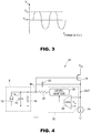
- the output node OUT is biased at a voltage value relatively close to the supply voltage V DD . Consequently, if we designate the voltage present on the output node OUT in the presence of an acoustic signal that reaches the MEMS transducer 8 with V tot , it may occur that, as the amplitude of the acoustic signal increases, the voltage V tot reaches the supply voltage V DD and hence undergoes clipping, as illustrated by way of example in Figure 3 . In other words, the voltage V tot is no longer directly proportional to the charge present in the transduction capacitor 14, but rather saturated to a value equal to the supply voltage V DD . Therefore, the operation of amplification performed by the readout circuit 10 introduces a high distortion.
- the document GB2560588 discloses a voltage amplifying circuit for a capacitive transducer, which includes a transistor acting as a buffer (i.e., with a unitary gain), downstream of which an operational amplifier is present, which acts as a feedback element.
- a transistor acting as a buffer i.e., with a unitary gain
- an operational amplifier which acts as a feedback element.
- Such a solution just adds a DC voltage on the output node, represented by the source terminal of the abovementioned transistor, without this allowing to prevent the saturation of the output voltage to the supply voltage.
- the aim of the present invention is therefore to provide an electronic circuit that will solve at least in part the drawbacks of the prior art.
- a charge amplifier circuit is provided, as defined in the annexed claims.
- the present circuit is based on the idea of decoupling the biasing voltages of the input node IN and of the output node OUT of the readout circuit, as illustrated schematically in Figure 4 , where elements already present in Figure 2 are designated by the same reference signs, unless specified otherwise.
- the readout circuit, designated by 30, is described limitedly to the differences with respect to what is illustrated in Figure 1 .
- the readout circuit 30 comprises a feedback circuit 32, which in turn comprises a control circuit 34 and a level shifter 36.
- the control circuit 34 comprises a first input, connected to the output node OUT, and a second input, which in use is set at a reference voltage V ref .
- the reference voltage V ref is directly proportional to the supply voltage V DD , or is generated by using a corresponding bandgap circuit (not illustrated).
- V ref 0.5 ⁇ V DD
- the reference voltage V ref is generated starting from the supply voltage V DD by means of a resistive divider (not shown) .
- the level shifter 36 is connected between the second terminal of the feedback resistor 22 and the output node OUT. Furthermore, the level shifter 36 is operatively connected to the output of the control circuit 34, as described hereinafter.
- the resistance of the feedback resistor 22 ranges, for example, between 100 G ⁇ and 1 T ⁇ .
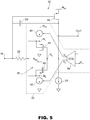
- the level shifter 36 comprises a respective pair of variable-current generators 40, 42, referred to hereinafter as the "first level-shift generator 40" and the “second level-shift generator 42", as well as a pair of respective MOSFETs 44, 46, referred to hereinafter as the “first level-shift transistor 44” and the “second level-shift transistor 46".
- the first level-shift transistor 44 is of the P-channel enhancement-mode type; the second level-shift transistor 46 is of the N-channel depletion-mode type (also known as "native N-channel transistor"). Furthermore, the first and the second level-shift transistors 44, 46 are, for example, of the type with source terminal connected to the bulk.
- the first level-shift generator 40 has a first and a second conduction terminal, which are connected to the supply node N DD and to the source terminal, respectively, of the first level-shift transistor 44, which forms a first internal node N 1 , which electrically coincides with the second terminal of the feedback resistor 22. Furthermore, the first level-shift generator 40 has a control terminal, which is connected to a first output of the control circuit 34.
- the second level-shift generator 42 has a first and a second conduction terminal, which are connected to the source terminal of the second level-shift transistor 46 and to the ground, respectively, of the readout circuit 30.
- the source terminal of the second level-shift transistor 46 forms a second internal node N 2 , which electrically coincides with the second terminal of the feedback resistor 22, and therefore also with the first internal node N 1 .
- the second level-shift generator 42 has a respective control terminal, which is connected to a second output of the control circuit 34.
- the drain terminals of the first and of the second level-shift transistors 44, 46 are connected to the ground of the readout circuit 30 and to the supply node N DD , respectively.
- the gate terminals of the first and of the second level-shift transistors 44, 46 are connected together so as to form a third internal node N 3 , which electrically coincides with the output node OUT.
- control circuit 34 supplies on its own first and second outputs, respectively, a first and a second control signal V C , V C ', which, as described in greater detail hereinafter, depend upon the difference between the output biasing voltage V CMO and the reference voltage V ref , so as to form a closed control loop.
- V C , V C ' a first and a second control signal
- the readout circuit 30 also comprises a pair of transistors 140, 142, referred to hereinafter respectively as “injection transistor 140" and “pick-up transistor 142".
- the injection transistor 140 is a P-channel enhancement-mode MOSFET, which performs the function of the first level-shift generator 40.
- the source and drain terminals of the injection transistor 140 are connected to the supply node N DD and to the first internal node N 1 , respectively.
- the pick-up transistor 142 is an N-channel depletion-mode MOSFET, which performs the function of the second level-shift generator 42.
- the source and drain terminals of the injection transistor 140 are connected to the second internal node N 2 and to the supply node N DD , respectively.
- the control circuit 34 is formed by an operational amplifier, and hence comprises a differential pair formed by a first and a second MOSFET 51, 52, referred to hereinafter as the "first control transistor 51” and the “second control transistor 52", respectively.
- the first and the second control transistors 51, 52 are P-channel enhancement-mode MOSFETs, the source terminals of which are connected together.
- the control circuit 34 further comprises a respective current generator 154, referred to hereinafter as "control generator 154".
- control generator 154 is interposed between the supply node N DD and the source terminals of the first and the second control transistors 51, 52.
- the control generator 154 generates a constant current I tot , which divides between the first and the second control transistors 51, 52 as a function of the voltages present on the respective gate terminals, as described hereinafter.
- the gate terminal of the first control transistor 51 is connected to the third internal node N 3 , and therefore also to the output node OUT (not shown in Figure 6 ), and the gate terminal of the second control transistor 52 is set at the reference voltage V ref .
- the control circuit 34 further comprises a third, a fourth, a fifth and a sixth control transistor 53, 54, 55, 56.
- the third, the fourth and the fifth control transistors 53, 54, 55 are N-channel enhancement-mode MOSFETs; the sixth control transistor 56 is a P-channel enhancement-mode MOSFET. Furthermore, the third, the fourth and the sixth control transistors 53, 54, 56 are diode-connected; i.e., they have the respective drain terminals connected to the respective gate terminals.
- the drain terminals of the third and fourth control transistors 53, 54 are connected to the drain terminals of the first and the second control transistors 51, 52, respectively, and the source terminals of the third and the fourth control transistors 53, 54 are connected to the ground of the readout circuit 30.
- the gate terminals of the third and the fourth control transistors 53, 54 are connected to the gate terminal of the pick-up transistor 142 and to the gate terminal of the fifth control transistor 55, respectively.
- the source and drain terminals of the fifth control transistor 55 are connected to the ground of the readout circuit 30 and to the drain terminal of the sixth control transistor 56, respectively.
- the gate and source terminals of the sixth control transistor 56 are connected to the gate terminal of the injection transistor 140 and to the supply node N DD , respectively.
- the third control transistor 53 and the pick-up transistor 142 form a first current mirror, which purely by way of example has a unitary mirroring ratio. Consequently, if I 1 is the current that flows in the first control transistor 51, then also the current that flows in the pick-up transistor 142 is equal to the current I 1 . In other words, the current drawn by the pick-up transistor 142 from the second internal node N 2 , and therefore from the second level-shift transistor 46, is equal to the current I 1 .
- the fourth and fifth control transistors 54, 55 form a second current mirror, which purely by way of example has a unitary mirroring ratio. Consequently, if I 2 is the current that flows in the second control transistor 52, then also the current that flows in the fifth control transistor 55 is equal to the current I 2 . In addition, the sum of the currents I 1 and I 2 is equal to the current I tot .
- the sixth control transistor 56 and the injection transistor 140 form a third current mirror, which purely by way of example has a unitary mirroring ratio. Therefore, the current that flows in the injection transistor 140 is equal to the current I 2 . In other words, the current injected into the first internal node N 1 , and therefore into the first level-shift transistor 44, by the injection transistor 140 is equal to the current I 2 .
- the voltages on the gate terminals of the injection transistor 140 and of the pick-up transistor 142 represent the aforementioned first and second control signals V C , V C '.
- the first and the second level-shift transistors 44, 46 operate as voltage followers, since the voltage variations on the respective source terminals follow the voltage variations on the respective gate terminals (and vice versa) . Furthermore, in the feedback resistor 22 current does not flow (either in the presence or in the absence of acoustic signals), and the first and the second internal nodes N 1 , N 2 are at a voltage equal to V DD -
- the control circuit 34 functions as a transconductance operational amplifier, which detects the difference between the output biasing voltage V CMO , present on the third internal node N 3 , and the reference voltage V ref , consequently controlling the injection transistor 140 and the pick-up transistor 142 so as to vary the current that is injected into the first level-shift transistor 44 and the current that is drawn from the second level-shift transistor 46.
- the variations of the current injected into the first level-shift transistor 44 and of the current drawn from the second level-shift transistor 46 cause consequent variations of the voltages of the source terminals of the first and the second level-shift transistors 44, 46.
- the voltage on the gate terminal of the latter, and therefore on the first internal node N 1 decreases.
- the voltage on the gate terminal of the latter, and therefore on the second internal node N 2 increases.
- the output biasing voltage V CMO present on the third internal node N 3 , is found to be a combination of the input biasing voltage V CMI , present on the input node IN, and any one of the gate-to-source voltages of the first and the second level-shift transistors 44, 46.
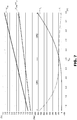
- Figure 7 shows an example of the plots of the input biasing voltage V CMI and of the output biasing voltage V CMO , as a function of the supply voltage V DD , as well as the plots of the currents I 1 and I 2 , i.e., of the currents that flow in the second level-shift transistor 46 and in the first level-shift transistor 44, respectively.
- the current I 2 is to a first approximation negligible, and hence the first level-shift transistor 44 is inhibited, unlike the second level-shift transistor 46, which operates in saturation; instead, for relatively high values of the supply voltage V DD , the current I 1 becomes to a first approximation negligible, and therefore the second level-shift transistor 46 is inhibited, whereas the first level-shift transistor 44 operates in saturation.
- the second level-shift transistor 46 follows, for low values of the supply voltage V DD , the reference voltage V ref , varying the voltage on its gate terminal accordingly.
- the output biasing voltage V CMO is imposed by the second level-shift transistor 46, which prevails over the first level-shift transistor 44.
- the first level-shift transistor 44 is inhibited as, due to its threshold voltage (for example, with a modulus equal to 650 mV), there is no sufficient voltage difference between its source and gate terminals.
- the first level-shift transistor 46 switches on and tends to prevail over the first level-shift transistor 44, feeding back onto its own gate terminal the voltage present on its own source terminal minus the absolute value of its own gate-to-source voltage. In this way, the difficulty of significantly raising, by the second level-shift transistor 46, the voltage on its own gate terminal, is obviated even when the transistor 46 is crossed by a high current.
- the voltage regions in which, the first and the second level-shift transistors 44, 46 prevail are designated by OR2 and OR1, respectively.
- Figure 7 also shows how the output biasing voltage V CMO and the reference voltage V ref are substantially equal, since it is assumed that the gain of the loop that controls the output biasing voltage V CMO as a function of the difference of the latter with respect to the reference voltage V ref is high.
- the output biasing voltage V CMO does not follow, but for an approximately constant offset, the supply voltage V DD . Instead, the output biasing voltage V CMO is directly proportional to the supply voltage V DD , which guarantees an increase of the output dynamic range, in addition to a decoupling from the input biasing voltage V CMI .
- the output biasing voltage V CMO is set through a closed control loop, hence in a particularly accurate way.
- the readout circuit 30 maintains a high input impedance and, for small signals, maintains the same transfer function (understood as ratio between the output voltage V out and the charge generated by the transducer).
- V out -q/Cf
- q designates the charge generated by the MEMS transducer 8
- Cf designates the capacitance of the feedback capacitor 20.
- Figure 8 shows a possible alternative, which is now described limitedly to the differences with respect to what is illustrated in Figure 6 .
- This alternative does not envisage the use of depletion transistors, and is hence suited to being manufactured in the simplest way in comparison to what is illustrated in Figure 6 , for example by using standard CMOS manufacturing technologies.
- the second level-shift transistor here designated by 246, is of the N-channel enhancement-mode type, and hence has a threshold voltage higher than in the case illustrated in Figure 6 .
- the gate terminal of the second level-shift transistor 246 is connected to a fourth internal node N 4 , instead of to the third internal node N 3 .
- the source terminals of the injection transistor 140 and of the sixth control transistor 56 and the drain terminal of the second level-shift transistor 246 are connected to an additional supply node N DDls , which is set at an additional supply voltage V DDls , which is such that V DDls ⁇ V DD + ⁇ V, with ⁇ V at least equal, for example, to 100 mV.
- the control generator 154 is interposed between the additional supply node N DDls and the source terminals of the first and the second control transistors 51, 52.
- the readout circuit 30 comprises a first, a second, a third and a fourth additional transistor 201, 202, 203, 204.
- the first additional transistor 201 is a N-channel enhancement-mode MOSFET, the source terminal of which is connected to the ground of the readout circuit 30, and the gate terminal of which is connected to the gate terminal of the third control transistor 53 so as to form a fourth current mirror, which purely by way of example has a unitary mirroring ratio.
- the second, the third and the fourth additional transistors 202, 203, 204 are P-channel enhancement-mode MOSFETs. Furthermore, the second additional transistor 202 is of the type with source terminal connected to the bulk.
- the gate terminals of the third and of the fourth additional transistors 203, 204 are connected together. Furthermore, the source terminals of the third and of the fourth additional transistors 203, 204 are connected to the additional supply node N DDls .
- the drain terminal of the third additional transistor 203 is connected to the drain terminal of the first additional transistor 201, as well as to the gate terminal of the third additional transistor 203, which is hence diode-connected.
- the drain terminal of the fourth additional transistor 204 and the source terminal of the second additional transistor 202 are connected to the fourth internal node N 4 .
- the gate terminal and the drain terminal of the second additional transistor 202 are connected to the third internal node N 3 and to the ground of the readout circuit 30, respectively.
- the fourth current mirror flowing in the first additional transistor 201 is the current I 1 , which flows also in the second and fourth additional transistors 202, 204, since the third and fourth additional transistors 203, 204 form a fifth current mirror, which purely by way of example has a unitary mirroring ratio.
- the voltage on the fourth internal node N 4 is equal to the voltage present on the second internal node N 2 , plus the gate-to-source voltage of the second level-shift transistor 246.
- the voltage on the third internal node N 3 is equal to the voltage present on the fourth internal node N 4 minus the absolute value of the gate-to-source voltage of the second additional transistor 202, which to a first approximation is equal to the absolute value of the gate-to-source voltage of the second level-shift transistor 246.
- the plots of the voltage on the third internal node N 3 and of the currents I 1 and I 2 remain substantially the same as what has been described with reference to the embodiment illustrated in Figure 6 .
- the mirroring ratios of one or more of the current mirrors may not be unitary ratios.
- MOSFET 18 instead of the MOSFET 18 a circuit including an operational amplifier (not illustrated) may be present.
Landscapes
- Engineering & Computer Science (AREA)
- Power Engineering (AREA)
- Physics & Mathematics (AREA)
- Acoustics & Sound (AREA)
- Signal Processing (AREA)
- Computer Hardware Design (AREA)
- General Engineering & Computer Science (AREA)
- Mathematical Physics (AREA)
- Computing Systems (AREA)
- Multimedia (AREA)
- Amplifiers (AREA)
- Measuring Fluid Pressure (AREA)
- Electrostatic, Electromagnetic, Magneto- Strictive, And Variable-Resistance Transducers (AREA)
Abstract
Description
- The present invention relates to a charge amplifier circuit with a high output dynamic range, which can be coupled to a MEMS (MicroElectroMechanical System) sensor.
- Today microelectromechanical devices, known simply as MEMS devices, are very widespread.
- MEMS devices can perform the most disparate functions. For example, MEMS microphones are known, each of which is formed, as illustrated in
Figure 1 , by a first and asecond pad MEMS transducer 8, formed in thefirst pad 2, and anintegrated circuit 10, formed in thesecond pad 4. The integratedcircuit 10 is usually of an ASIC (Application-Specific Integrated Circuit) type and is commonly known as "readout circuit 10". - The
MEMS transducer 8 includes a membrane (not illustrated) adapted to undergo deformation in the presence of an acoustic signal (stimulus) coming from the outside. Furthermore, theMEMS transducer 8 is, for example, of a piezoelectric type; i.e., it includes at least one piezoelectric region (not illustrated), which is operatively coupled to the membrane and is adapted to generate an electrical charge as a function of the deformation of the membrane. From an electrical point of view, theMEMS transducer 8 can hence be modelled as shown inFigure 2 , which illustrates a variable-current generator 12, which is configured to inject a current into atransduction capacitor 14 and into atransduction resistor 16, which are connected in parallel; this current is a function of the deformation of the membrane. - In particular, the term "transduction node NT" indicates the node into which the variable-
current generator 12 injects the current, thetransduction capacitor 14, thetransduction resistor 16, and the variable-current generator 12 are set between the transduction node NT and the ground of theMEMS transducer 8. - The
readout circuit 10 is electrically coupled to theMEMS transducer 8 so as to convert the charge generated by theMEMS transducer 8 into an output voltage Vout. - The
readout circuit 10 therefore acts as an amplifier, preferably of the low-noise type. Furthermore, thereadout circuit 10 is characterized by a low current consumption and by a high AOP (Acoustic-Overload Point), understood as the amplitude of the input acoustic level such that the THD (Total Harmonic Distortion) reaches 10%. - An example of implementation of the
readout circuit 10 is illustrated once again inFigure 2 . - In particular, the
readout circuit 10 comprises aMOSFET 18 of the P-channel enhancement-mode type. The source terminal of theMOSFET 18 is connected to a supply node NDD, which in use is set at a supply voltage VDD. The gate terminal of theMOSFET 18 forms an input node IN of thereadout circuit 10; the drain terminal of theMOSFET 18 forms an output node OUT of thereadout circuit 10. - The
readout circuit 10 also comprises acapacitor 20 and aresistor 22, which are referred to hereinafter as "feedback capacitor 20" and "feedback resistor 22", respectively. - The
feedback capacitor 20 and thefeedback resistor 22 are connected in parallel between the input node IN and the output node OUT of thereadout circuit 10. In particular, a first terminal of thefeedback resistor 22 is connected to the input node IN, whereas a second terminal of thefeedback resistor 22 is connected to the output node OUT. Furthermore, the input node IN is connected to the transduction node NT, and in particular electrically coincides with the latter. - The
readout circuit 10 also comprises a respectivecurrent generator 24, which is connected between the output node OUT and the ground of thereadout circuit 10 and generates a constant current, directed towards the ground of thereadout circuit 10. - That said, since the
transduction resistor 16 and thefeedback resistor 22 have particularly high values, the input node IN and the output node OUT are biased, respectively, at an input biasing voltage VCMI and at an output biasing voltage VCMO, which are equal to each other and are set, respectively, by the threshold voltage of theMOSFET 18 and by the current that flows in theMOSFET 18. In greater detail, if we designate the gate-to-source voltage of theMOSFET 18 with VGS, we have VCMI =VCMO=VDD - |VGS|. - The output biasing voltage VCMO represents the so-called output quiescent level, i.e., the voltage value supplied by the
readout circuit 10 in the absence of acoustic signals on theMEMS transducer 8. - In practice, the output node OUT is biased at a voltage value relatively close to the supply voltage VDD. Consequently, if we designate the voltage present on the output node OUT in the presence of an acoustic signal that reaches the
MEMS transducer 8 with Vtot, it may occur that, as the amplitude of the acoustic signal increases, the voltage Vtot reaches the supply voltage VDD and hence undergoes clipping, as illustrated by way of example inFigure 3 . In other words, the voltage Vtot is no longer directly proportional to the charge present in thetransduction capacitor 14, but rather saturated to a value equal to the supply voltage VDD. Therefore, the operation of amplification performed by thereadout circuit 10 introduces a high distortion. - The document
GB2560588 - The aim of the present invention is therefore to provide an electronic circuit that will solve at least in part the drawbacks of the prior art.
- According to the present invention, a charge amplifier circuit is provided, as defined in the annexed claims.
- For a better understanding of the present invention, preferred embodiments thereof are now described, purely by way of non-limiting example and with reference to the attached drawings, wherein:
-
Figure 1 shows a block diagram of a MEMS device; -
Figure 2 shows an equivalent circuit diagram of the MEMS device illustrated inFigure 1 ; -
Figure 3 shows an example of plot of an analog signal, as a function of an electrical charge; -
Figure 4 shows a principle circuit diagram of the present electronic circuit, coupled to a sensor; -
Figure 5 shows a circuit diagram of the present electronic circuit, with parts represented schematically in terms of working principle; -
Figures 6 and8 show circuit diagrams of embodiments of the present electronic circuit; and -
Figure 7 shows plots of voltages and currents generated within the present electronic circuit, as a function of a supply voltage VDD. - The present circuit is based on the idea of decoupling the biasing voltages of the input node IN and of the output node OUT of the readout circuit, as illustrated schematically in
Figure 4 , where elements already present inFigure 2 are designated by the same reference signs, unless specified otherwise. In addition, the readout circuit, designated by 30, is described limitedly to the differences with respect to what is illustrated inFigure 1 . - In detail, the
readout circuit 30 comprises afeedback circuit 32, which in turn comprises acontrol circuit 34 and alevel shifter 36. - The
control circuit 34 comprises a first input, connected to the output node OUT, and a second input, which in use is set at a reference voltage Vref. As described in greater detail hereinafter, the reference voltage Vref is directly proportional to the supply voltage VDD, or is generated by using a corresponding bandgap circuit (not illustrated). In what follows it is assumed, purely by way of example, that the relation Vref = 0.5 ∗ VDD applies, and that the reference voltage Vref is generated starting from the supply voltage VDD by means of a resistive divider (not shown) . - The
level shifter 36 is connected between the second terminal of thefeedback resistor 22 and the output node OUT. Furthermore, thelevel shifter 36 is operatively connected to the output of thecontrol circuit 34, as described hereinafter. The resistance of thefeedback resistor 22 ranges, for example, between 100 GΩ and 1 TΩ. - As shown in
Figure 5 , thelevel shifter 36 comprises a respective pair of variable-current generators shift generator 40" and the "second level-shift generator 42", as well as a pair ofrespective MOSFETs shift transistor 44" and the "second level-shift transistor 46". - The first level-
shift transistor 44 is of the P-channel enhancement-mode type; the second level-shift transistor 46 is of the N-channel depletion-mode type (also known as "native N-channel transistor"). Furthermore, the first and the second level-shift transistors - In detail, the first level-
shift generator 40 has a first and a second conduction terminal, which are connected to the supply node NDD and to the source terminal, respectively, of the first level-shift transistor 44, which forms a first internal node N1, which electrically coincides with the second terminal of thefeedback resistor 22. Furthermore, the first level-shift generator 40 has a control terminal, which is connected to a first output of thecontrol circuit 34. - The second level-
shift generator 42 has a first and a second conduction terminal, which are connected to the source terminal of the second level-shift transistor 46 and to the ground, respectively, of thereadout circuit 30. The source terminal of the second level-shift transistor 46 forms a second internal node N2, which electrically coincides with the second terminal of thefeedback resistor 22, and therefore also with the first internal node N1. In addition, the second level-shift generator 42 has a respective control terminal, which is connected to a second output of thecontrol circuit 34. - The drain terminals of the first and of the second level-
shift transistors readout circuit 30 and to the supply node NDD, respectively. The gate terminals of the first and of the second level-shift transistors - In greater detail, the
control circuit 34 supplies on its own first and second outputs, respectively, a first and a second control signal VC, VC', which, as described in greater detail hereinafter, depend upon the difference between the output biasing voltage VCMO and the reference voltage Vref, so as to form a closed control loop. In this regard, the possible contribution due to the presence of a (small signal) output voltage Vout is irrelevant, since said contribution would fall outside the frequency band in which thecontrol circuit 34 operates. - As illustrated in
Figure 6 , thereadout circuit 30 also comprises a pair oftransistors injection transistor 140" and "pick-up transistor 142". - In particular, the
injection transistor 140 is a P-channel enhancement-mode MOSFET, which performs the function of the first level-shift generator 40. For this purpose, the source and drain terminals of theinjection transistor 140 are connected to the supply node NDD and to the first internal node N1, respectively. - The pick-
up transistor 142 is an N-channel depletion-mode MOSFET, which performs the function of the second level-shift generator 42. For this purpose, the source and drain terminals of theinjection transistor 140 are connected to the second internal node N2 and to the supply node NDD, respectively. - As illustrated again in
Figure 6 , thecontrol circuit 34 is formed by an operational amplifier, and hence comprises a differential pair formed by a first and asecond MOSFET first control transistor 51" and the "second control transistor 52", respectively. In particular, the first and thesecond control transistors - The
control circuit 34 further comprises a respectivecurrent generator 154, referred to hereinafter as "control generator 154". In particular, thecontrol generator 154 is interposed between the supply node NDD and the source terminals of the first and thesecond control transistors control generator 154 generates a constant current Itot, which divides between the first and thesecond control transistors first control transistor 51 is connected to the third internal node N3, and therefore also to the output node OUT (not shown inFigure 6 ), and the gate terminal of thesecond control transistor 52 is set at the reference voltage Vref. - The
control circuit 34 further comprises a third, a fourth, a fifth and asixth control transistor - In detail, the third, the fourth and the
fifth control transistors sixth control transistor 56 is a P-channel enhancement-mode MOSFET. Furthermore, the third, the fourth and thesixth control transistors - In greater detail, the drain terminals of the third and
fourth control transistors second control transistors fourth control transistors readout circuit 30. The gate terminals of the third and thefourth control transistors transistor 142 and to the gate terminal of thefifth control transistor 55, respectively. The source and drain terminals of thefifth control transistor 55 are connected to the ground of thereadout circuit 30 and to the drain terminal of thesixth control transistor 56, respectively. The gate and source terminals of thesixth control transistor 56 are connected to the gate terminal of theinjection transistor 140 and to the supply node NDD, respectively. - In practice, the
third control transistor 53 and the pick-uptransistor 142 form a first current mirror, which purely by way of example has a unitary mirroring ratio. Consequently, if I1 is the current that flows in thefirst control transistor 51, then also the current that flows in the pick-uptransistor 142 is equal to the current I1. In other words, the current drawn by the pick-uptransistor 142 from the second internal node N2, and therefore from the second level-shift transistor 46, is equal to the current I1. - The fourth and
fifth control transistors second control transistor 52, then also the current that flows in thefifth control transistor 55 is equal to the current I2. In addition, the sum of the currents I1 and I2 is equal to the current Itot. - The
sixth control transistor 56 and theinjection transistor 140 form a third current mirror, which purely by way of example has a unitary mirroring ratio. Therefore, the current that flows in theinjection transistor 140 is equal to the current I2. In other words, the current injected into the first internal node N1, and therefore into the first level-shift transistor 44, by theinjection transistor 140 is equal to the current I2. - In practice, the voltages on the gate terminals of the
injection transistor 140 and of the pick-uptransistor 142 represent the aforementioned first and second control signals VC, VC'. - In use, the first and the second level-
shift transistors feedback resistor 22 current does not flow (either in the presence or in the absence of acoustic signals), and the first and the second internal nodes N1, N2 are at a voltage equal to VDD - |VGS|, where, as mentioned previously, VGS is the gate-to-source voltage of theMOSFET 18. - The
control circuit 34 functions as a transconductance operational amplifier, which detects the difference between the output biasing voltage VCMO, present on the third internal node N3, and the reference voltage Vref, consequently controlling theinjection transistor 140 and the pick-uptransistor 142 so as to vary the current that is injected into the first level-shift transistor 44 and the current that is drawn from the second level-shift transistor 46. - The variations of the current injected into the first level-
shift transistor 44 and of the current drawn from the second level-shift transistor 46 cause consequent variations of the voltages of the source terminals of the first and the second level-shift transistors shift transistor 44 increases, the voltage on the gate terminal of the latter, and therefore on the first internal node N1, decreases. Furthermore, as the current tapped from the second level-shift transistor 46 increases, the voltage on the gate terminal of the latter, and therefore on the second internal node N2, increases. Since, in each of the first and the second level-shift transistors shift transistors -
Figure 7 shows an example of the plots of the input biasing voltage VCMI and of the output biasing voltage VCMO, as a function of the supply voltage VDD, as well as the plots of the currents I1 and I2, i.e., of the currents that flow in the second level-shift transistor 46 and in the first level-shift transistor 44, respectively. It may be noted that, for relatively low values of the supply voltage VDD, the current I2 is to a first approximation negligible, and hence the first level-shift transistor 44 is inhibited, unlike the second level-shift transistor 46, which operates in saturation; instead, for relatively high values of the supply voltage VDD, the current I1 becomes to a first approximation negligible, and therefore the second level-shift transistor 46 is inhibited, whereas the first level-shift transistor 44 operates in saturation. - In practice, thanks to an extremely low threshold voltage, the second level-
shift transistor 46 follows, for low values of the supply voltage VDD, the reference voltage Vref, varying the voltage on its gate terminal accordingly. In other words, the output biasing voltage VCMO is imposed by the second level-shift transistor 46, which prevails over the first level-shift transistor 44. In particular, the first level-shift transistor 44 is inhibited as, due to its threshold voltage (for example, with a modulus equal to 650 mV), there is no sufficient voltage difference between its source and gate terminals. - Next, as the supply voltage VDD increases, the first level-
shift transistor 46 switches on and tends to prevail over the first level-shift transistor 44, feeding back onto its own gate terminal the voltage present on its own source terminal minus the absolute value of its own gate-to-source voltage. In this way, the difficulty of significantly raising, by the second level-shift transistor 46, the voltage on its own gate terminal, is obviated even when thetransistor 46 is crossed by a high current. InFigure 7 , the voltage regions in which, the first and the second level-shift transistors -
Figure 7 also shows how the output biasing voltage VCMO and the reference voltage Vref are substantially equal, since it is assumed that the gain of the loop that controls the output biasing voltage VCMO as a function of the difference of the latter with respect to the reference voltage Vref is high. - From what has been described and illustrated previously, the advantages that the present solution affords are evident.
- In particular, in the
readout circuit 30, the output biasing voltage VCMO does not follow, but for an approximately constant offset, the supply voltage VDD. Instead, the output biasing voltage VCMO is directly proportional to the supply voltage VDD, which guarantees an increase of the output dynamic range, in addition to a decoupling from the input biasing voltage VCMI. - In other words, as the supply voltage VDD increases, we find a corresponding increase in the AOP.
- In addition, the output biasing voltage VCMO is set through a closed control loop, hence in a particularly accurate way.
- Moreover, the
readout circuit 30 maintains a high input impedance and, for small signals, maintains the same transfer function (understood as ratio between the output voltage Vout and the charge generated by the transducer). In this regard, it can be demonstrated that, in a small-signal regime, Vout=-q/Cf, where q designates the charge generated by theMEMS transducer 8 and Cf designates the capacitance of thefeedback capacitor 20. -
Figure 8 shows a possible alternative, which is now described limitedly to the differences with respect to what is illustrated inFigure 6 . This alternative does not envisage the use of depletion transistors, and is hence suited to being manufactured in the simplest way in comparison to what is illustrated inFigure 6 , for example by using standard CMOS manufacturing technologies. - In detail, the second level-shift transistor, here designated by 246, is of the N-channel enhancement-mode type, and hence has a threshold voltage higher than in the case illustrated in
Figure 6 . The gate terminal of the second level-shift transistor 246 is connected to a fourth internal node N4, instead of to the third internal node N3. In addition, the source terminals of theinjection transistor 140 and of thesixth control transistor 56 and the drain terminal of the second level-shift transistor 246 are connected to an additional supply node NDDls, which is set at an additional supply voltage VDDls, which is such that VDDls ≥ VDD + ΔV, with ΔV at least equal, for example, to 100 mV. Thecontrol generator 154 is interposed between the additional supply node NDDls and the source terminals of the first and thesecond control transistors - Moreover, the
readout circuit 30 comprises a first, a second, a third and a fourthadditional transistor - The first
additional transistor 201 is a N-channel enhancement-mode MOSFET, the source terminal of which is connected to the ground of thereadout circuit 30, and the gate terminal of which is connected to the gate terminal of thethird control transistor 53 so as to form a fourth current mirror, which purely by way of example has a unitary mirroring ratio. - The second, the third and the fourth
additional transistors additional transistor 202 is of the type with source terminal connected to the bulk. - In particular, the gate terminals of the third and of the fourth
additional transistors additional transistors additional transistor 203 is connected to the drain terminal of the firstadditional transistor 201, as well as to the gate terminal of the thirdadditional transistor 203, which is hence diode-connected. - The drain terminal of the fourth
additional transistor 204 and the source terminal of the secondadditional transistor 202 are connected to the fourth internal node N4. The gate terminal and the drain terminal of the secondadditional transistor 202 are connected to the third internal node N3 and to the ground of thereadout circuit 30, respectively. - Thanks to the fourth current mirror, flowing in the first
additional transistor 201 is the current I1, which flows also in the second and fourthadditional transistors additional transistors - Operatively, the voltage on the fourth internal node N4 is equal to the voltage present on the second internal node N2, plus the gate-to-source voltage of the second level-
shift transistor 246. Furthermore, the voltage on the third internal node N3 is equal to the voltage present on the fourth internal node N4 minus the absolute value of the gate-to-source voltage of the secondadditional transistor 202, which to a first approximation is equal to the absolute value of the gate-to-source voltage of the second level-shift transistor 246. In this way, the plots of the voltage on the third internal node N3 and of the currents I1 and I2 remain substantially the same as what has been described with reference to the embodiment illustrated inFigure 6 . - The fact that the additional supply voltage VDDls is higher than the supply voltage VDD makes it possible to guarantee a correct drain-to-source voltage of the fourth
additional transistor 204, which, as also the other transistors, operates in saturation. - In conclusion, it is clear that further modifications and variations may be made to what has been described and illustrated herein, without thereby departing from the scope of the present invention, as defined in the annexed claims.
- For instance, the mirroring ratios of one or more of the current mirrors may not be unitary ratios.
- Instead of the MOSFET 18 a circuit including an operational amplifier (not illustrated) may be present.
- Finally, all the MOSFETs may have channels reversed with respect to what has been described.
Claims (8)
- A charge amplifier circuit couplable to a transducer (8) apt to generate an electrical charge that varies according to an external stimulus, said charge amplifier circuit (30) comprising:- an amplification stage (18) having an input node (IN), couplable to said transducer, and an output node (OUT), said amplification stage being configured to bias the input node (IN) at a first d.c. voltage (VCMI); and- a feedback circuit (22, 32), including a feedback capacitor (20), which is electrically interposed between the input and output nodes of the amplification stage;and wherein the feedback circuit further comprises:- a resistor (22) electrically coupled to the input node; and- a level-shifter circuit (34, 36), electrically interposed between the resistor and the output node and configured to bias the output node at a second d.c. voltage (VCMO), as a function of the difference between said second d.c. voltage and a reference voltage (Vref).
- The circuit according to claim 1, wherein the resistor (22) has a first terminal coupled to the input node (IN) of the amplification stage (18); and wherein the level-shifter circuit (34,36) comprises a first and a second MOSFET (44, 46; 44, 246), of the P-channel type and N-channel type, respectively, each of the first and the second MOSFETs having a respective conduction terminal coupled to a second terminal of the resistor, the control terminals of the first and of the second MOSFETs being coupled to the output node; and wherein the level-shifter circuit (34, 36) comprises a transconductance-amplifier circuit (36), which is configured to draw a first current (I1) from the second MOSFET and to inject a second current (I2) into the first MOSFET, as a function of said difference between the second d.c. voltage (VCMO) and the reference voltage (Vref).
- The circuit according to claim 2, wherein the second MOSFET (46) is of the depletion type; and wherein the first MOSFET (44) is of the enhancement type.
- The circuit according to claim 2, wherein the first and the second MOSFETs (44, 246) are of the enhancement type; and wherein the level-shifter circuit (34,36) further comprises an additional MOSFET (202), of the P-channel type; and wherein a conduction terminal and the control terminal of the additional MOSFET are coupled, respectively, to the control terminal of the second MOSFET and to the output node (OUT); and wherein the transconductance-amplifier circuit (36) is moreover configured to cause a current equal to said first current (I1) to flow in the additional MOSFET.
- The circuit according to any one of the claims 2 to 4, wherein the transconductance-amplifier circuit (36) comprises:- a differential pair (51, 52), which comprises a respective first transistor (51) and a respective second transistor (52), of a MOSFET type, the control terminal of the first transistor of the differential pair being coupled to the output node (OUT), the control terminal of the second transistor of the differential pair being set, in use, at said reference voltage (Vref); and- a mirror circuitry (53-56, 140, 142), coupled to the differential pair and to the first and to the second MOSFETs (44, 46; 44, 246) and configured so that said first and second currents (I1, I2) are, respectively, equal to the currents that flow in the first and in the second transistors of the differential pair.
- The circuit according to any one of the preceding claims, wherein the amplification stage (18) comprises a respective MOSFET (18); and wherein the control terminal of said respective MOSFET is coupled to the input node (IN) of the amplification stage; and wherein the first and the second conduction terminals of said respective MOSFET are coupled, respectively, to the output node (OUT) of the amplification stage and to a node set, in use, at a supply voltage (VDD).
- The circuit according to any one of the preceding claims, wherein the amplification stage (18) and the feedback capacitor (20) are configured so that, in use, on the output node (OUT), there is a variable voltage that depends upon said variable electrical charge through a coefficient that is, in modulus, inversely proportional to the capacitance of the feedback capacitor.
- An electronic device comprising the charge amplifier circuit (30) according to any one of the preceding claims and said transducer (8), said transducer being of a MEMS type.
Applications Claiming Priority (1)
| Application Number | Priority Date | Filing Date | Title |
|---|---|---|---|
| IT102019000001505A IT201900001505A1 (en) | 2019-02-01 | 2019-02-01 | CHARGE AMPLIFIER CIRCUIT WITH HIGH OUTPUT DYNAMICS FOR A MICROELECTROMECHANICAL SENSOR |
Publications (2)
| Publication Number | Publication Date |
|---|---|
| EP3691123A1 true EP3691123A1 (en) | 2020-08-05 |
| EP3691123B1 EP3691123B1 (en) | 2024-07-10 |
Family
ID=66166472
Family Applications (1)
| Application Number | Title | Priority Date | Filing Date |
|---|---|---|---|
| EP20154967.2A Active EP3691123B1 (en) | 2019-02-01 | 2020-01-31 | Charge amplifier circuit with a high output dynamic range for a microelectromechanical sensor |
Country Status (3)
| Country | Link |
|---|---|
| US (2) | US11177779B2 (en) |
| EP (1) | EP3691123B1 (en) |
| IT (1) | IT201900001505A1 (en) |
Families Citing this family (4)
| Publication number | Priority date | Publication date | Assignee | Title |
|---|---|---|---|---|
| IT201900001505A1 (en) * | 2019-02-01 | 2020-08-01 | St Microelectronics Srl | CHARGE AMPLIFIER CIRCUIT WITH HIGH OUTPUT DYNAMICS FOR A MICROELECTROMECHANICAL SENSOR |
| US11843907B1 (en) * | 2022-06-03 | 2023-12-12 | Infineon Technologies Ag | Linearization method applied to a MEMS microphone system |
| US12448275B2 (en) | 2022-06-10 | 2025-10-21 | Infineon Technologies Ag | Capacitive linearization method applied to MEMS microphones systems |
| WO2024150048A1 (en) * | 2023-01-12 | 2024-07-18 | Politecnico Di Milano | Charge preamplifier and radiation detection apparatus with wide dynamic range |
Citations (3)
| Publication number | Priority date | Publication date | Assignee | Title |
|---|---|---|---|---|
| GB2466776A (en) * | 2008-12-30 | 2010-07-07 | Wolfson Microelectronics Plc | Bootstrapping to reduce the effect of bond pad parasitic capacitance in a MEMS microphone circuit |
| US20150084694A1 (en) * | 2013-09-23 | 2015-03-26 | Sung-Ho Lee | Buffer circuit having an enhanced slew-rate and source driving circuit including the same |
| GB2560588A (en) | 2017-03-16 | 2018-09-19 | Cirrus Logic Int Semiconductor Ltd | MEMS transducer amplifiers |
Family Cites Families (20)
| Publication number | Priority date | Publication date | Assignee | Title |
|---|---|---|---|---|
| US5025226A (en) * | 1990-03-02 | 1991-06-18 | Triquint Semiconductor, Inc. | High-gain low-noise amplifier |
| US5777517A (en) * | 1995-09-13 | 1998-07-07 | Kabushiki Kaisha Toshiba | Semiconductor feedback amplifier having improved frequency characteristics |
| JP2004254071A (en) * | 2003-02-20 | 2004-09-09 | Nippon Telegr & Teleph Corp <Ntt> | Amplifier circuit |
| ATE410820T1 (en) * | 2004-01-12 | 2008-10-15 | Sonion As | AMPLIFIER CIRCUIT FOR CAPACITIVE CONVERTERS |
| US8254598B2 (en) * | 2007-06-12 | 2012-08-28 | Winbond Electronics Corporation | Programmable integrated microphone interface circuit |
| US8243956B2 (en) * | 2007-08-13 | 2012-08-14 | Gentex Corporation | Auto bias microphone system for use with multiple loads and method of forming same |
| US8335328B2 (en) * | 2007-10-24 | 2012-12-18 | Winbond Electronics Corporation | Programmable integrated microphone interface circuit |
| JP2010206237A (en) * | 2009-02-27 | 2010-09-16 | Panasonic Corp | Amplification device and sensor module |
| US8004366B2 (en) * | 2009-10-29 | 2011-08-23 | Texas Instruments Incorporated | Area and power efficient, high swing and monolitihic ground centered headphone amplifier circuit operable on a low voltage |
| JP2011233954A (en) * | 2010-04-23 | 2011-11-17 | Panasonic Corp | Amplifier for condenser microphone |
| JP2012039272A (en) * | 2010-08-05 | 2012-02-23 | Funai Electric Co Ltd | Microphone unit |
| KR101205512B1 (en) * | 2011-04-28 | 2012-11-28 | 주식회사 씨자인 | Electret condenser microphone with variable input impedance pre-amplifier and variable input impedance controlling method of the pre-amplifier |
| DE112012005578B4 (en) * | 2012-01-05 | 2019-11-07 | Tdk Corporation | Differential microphone and method for driving a differential microphone |
| US9300259B2 (en) * | 2012-04-04 | 2016-03-29 | Ams Ag | Sensor amplifier arrangement and method for amplification of a sensor signal |
| US10114114B2 (en) | 2014-09-15 | 2018-10-30 | Stmicroelectronics S.R.L. | Ultrasonic probe with precharge circuit and method of controlling an ultrasonic probe |
| US10145728B2 (en) | 2014-09-15 | 2018-12-04 | Stmicroelectronics S.R.L. | Reception and transmission circuit for a capacitive micromachined ultrasonic transducer |
| US20170077911A1 (en) * | 2015-09-11 | 2017-03-16 | Knowles Electronics, Llc | Method and Apparatus to Cancel an Offset Voltage |
| US10295576B2 (en) * | 2017-07-26 | 2019-05-21 | Akustica, Inc. | Ratiometric biasing for high impedance capacitive sensing |
| IT201900001505A1 (en) * | 2019-02-01 | 2020-08-01 | St Microelectronics Srl | CHARGE AMPLIFIER CIRCUIT WITH HIGH OUTPUT DYNAMICS FOR A MICROELECTROMECHANICAL SENSOR |
| US11240456B2 (en) * | 2019-06-14 | 2022-02-01 | Omnivision Technologies, Inc. | Column amplifier reset circuit |
-
2019
- 2019-02-01 IT IT102019000001505A patent/IT201900001505A1/en unknown
-
2020
- 2020-01-07 US US16/736,513 patent/US11177779B2/en active Active
- 2020-01-31 EP EP20154967.2A patent/EP3691123B1/en active Active
-
2021
- 2021-10-14 US US17/501,699 patent/US11824503B2/en active Active
Patent Citations (3)
| Publication number | Priority date | Publication date | Assignee | Title |
|---|---|---|---|---|
| GB2466776A (en) * | 2008-12-30 | 2010-07-07 | Wolfson Microelectronics Plc | Bootstrapping to reduce the effect of bond pad parasitic capacitance in a MEMS microphone circuit |
| US20150084694A1 (en) * | 2013-09-23 | 2015-03-26 | Sung-Ho Lee | Buffer circuit having an enhanced slew-rate and source driving circuit including the same |
| GB2560588A (en) | 2017-03-16 | 2018-09-19 | Cirrus Logic Int Semiconductor Ltd | MEMS transducer amplifiers |
Also Published As
| Publication number | Publication date |
|---|---|
| US11824503B2 (en) | 2023-11-21 |
| IT201900001505A1 (en) | 2020-08-01 |
| US20220038065A1 (en) | 2022-02-03 |
| US11177779B2 (en) | 2021-11-16 |
| US20200252035A1 (en) | 2020-08-06 |
| EP3691123B1 (en) | 2024-07-10 |
Similar Documents
| Publication | Publication Date | Title |
|---|---|---|
| US11824503B2 (en) | Charge amplifier circuit with a high output dynamic range for a microelectromechanical sensor | |
| CN103518323B (en) | Auto-zero offset buffer amplifier and auto-zero offset correction method thereof | |
| US4524328A (en) | MOS Power amplifier circuit | |
| KR100275177B1 (en) | Low-voltage differential amplifier | |
| US7948314B2 (en) | Tunable linear operational transconductance amplifier | |
| US3956708A (en) | MOSFET comparator | |
| US7446607B2 (en) | Regulated cascode circuit, an amplifier including the same, and method of regulating a cascode circuit | |
| US6353344B1 (en) | High impedance bias circuit | |
| US5113148A (en) | Linear CMOS output stage | |
| US6833760B1 (en) | Low power differential amplifier powered by multiple unequal power supply voltages | |
| US12199575B2 (en) | Super source follower | |
| EP1686686A1 (en) | Am intermediate frequency variable gain amplifier circuit, variable gain amplifier circuit, and semiconductor integrated circuit thereof | |
| US8890612B2 (en) | Dynamically biased output structure | |
| EP1355416B1 (en) | CMOS high impedance circuit | |
| KR20050034596A (en) | Amplification circuit | |
| US20070222532A1 (en) | Temperature-compensated crystal oscillator | |
| JP4785243B2 (en) | Cascode amplifier circuit and folded cascode amplifier circuit | |
| US11101776B2 (en) | Common source preamplifier for a MEMS capacitive sensor | |
| US9246455B2 (en) | Three stage amplifier | |
| US6496066B2 (en) | Fully differential operational amplifier of the folded cascode type | |
| US20120207331A1 (en) | Preamplifier circuit and microphone having the same | |
| EP4290882A1 (en) | A capacitive linearization method applied to mems microphones systems | |
| US11437962B2 (en) | Differential amplifier circuit having variable gain | |
| JPH0612856B2 (en) | Amplifier circuit | |
| US6542034B2 (en) | Operational amplifier with high gain and symmetrical output-current capability |
Legal Events
| Date | Code | Title | Description |
|---|---|---|---|
| PUAI | Public reference made under article 153(3) epc to a published international application that has entered the european phase |
Free format text: ORIGINAL CODE: 0009012 |
|
| STAA | Information on the status of an ep patent application or granted ep patent |
Free format text: STATUS: THE APPLICATION HAS BEEN PUBLISHED |
|
| AK | Designated contracting states |
Kind code of ref document: A1 Designated state(s): AL AT BE BG CH CY CZ DE DK EE ES FI FR GB GR HR HU IE IS IT LI LT LU LV MC MK MT NL NO PL PT RO RS SE SI SK SM TR |
|
| AX | Request for extension of the european patent |
Extension state: BA ME |
|
| STAA | Information on the status of an ep patent application or granted ep patent |
Free format text: STATUS: REQUEST FOR EXAMINATION WAS MADE |
|
| 17P | Request for examination filed |
Effective date: 20210201 |
|
| RBV | Designated contracting states (corrected) |
Designated state(s): AL AT BE BG CH CY CZ DE DK EE ES FI FR GB GR HR HU IE IS IT LI LT LU LV MC MK MT NL NO PL PT RO RS SE SI SK SM TR |
|
| STAA | Information on the status of an ep patent application or granted ep patent |
Free format text: STATUS: EXAMINATION IS IN PROGRESS |
|
| 17Q | First examination report despatched |
Effective date: 20211210 |
|
| GRAP | Despatch of communication of intention to grant a patent |
Free format text: ORIGINAL CODE: EPIDOSNIGR1 |
|
| RIC1 | Information provided on ipc code assigned before grant |
Ipc: H04R 1/04 20060101ALI20231011BHEP Ipc: H03F 3/45 20060101ALI20231011BHEP Ipc: H03F 3/345 20060101ALI20231011BHEP Ipc: H03F 3/183 20060101ALI20231011BHEP Ipc: H03F 3/30 20060101ALI20231011BHEP Ipc: H03F 3/70 20060101AFI20231011BHEP |
|
| STAA | Information on the status of an ep patent application or granted ep patent |
Free format text: STATUS: GRANT OF PATENT IS INTENDED |
|
| INTG | Intention to grant announced |
Effective date: 20231116 |
|
| GRAJ | Information related to disapproval of communication of intention to grant by the applicant or resumption of examination proceedings by the epo deleted |
Free format text: ORIGINAL CODE: EPIDOSDIGR1 |
|
| STAA | Information on the status of an ep patent application or granted ep patent |
Free format text: STATUS: EXAMINATION IS IN PROGRESS |
|
| GRAP | Despatch of communication of intention to grant a patent |
Free format text: ORIGINAL CODE: EPIDOSNIGR1 |
|
| STAA | Information on the status of an ep patent application or granted ep patent |
Free format text: STATUS: GRANT OF PATENT IS INTENDED |
|
| INTC | Intention to grant announced (deleted) | ||
| INTG | Intention to grant announced |
Effective date: 20240208 |
|
| GRAS | Grant fee paid |
Free format text: ORIGINAL CODE: EPIDOSNIGR3 |
|
| GRAA | (expected) grant |
Free format text: ORIGINAL CODE: 0009210 |
|
| STAA | Information on the status of an ep patent application or granted ep patent |
Free format text: STATUS: THE PATENT HAS BEEN GRANTED |
|
| AK | Designated contracting states |
Kind code of ref document: B1 Designated state(s): AL AT BE BG CH CY CZ DE DK EE ES FI FR GB GR HR HU IE IS IT LI LT LU LV MC MK MT NL NO PL PT RO RS SE SI SK SM TR |
|
| REG | Reference to a national code |
Ref country code: CH Ref legal event code: EP |
|
| REG | Reference to a national code |
Ref country code: DE Ref legal event code: R096 Ref document number: 602020033597 Country of ref document: DE |
|
| REG | Reference to a national code |
Ref country code: LT Ref legal event code: MG9D |
|
| REG | Reference to a national code |
Ref country code: NL Ref legal event code: MP Effective date: 20240710 |
|
| PG25 | Lapsed in a contracting state [announced via postgrant information from national office to epo] |
Ref country code: PT Free format text: LAPSE BECAUSE OF FAILURE TO SUBMIT A TRANSLATION OF THE DESCRIPTION OR TO PAY THE FEE WITHIN THE PRESCRIBED TIME-LIMIT Effective date: 20241111 |
|
| REG | Reference to a national code |
Ref country code: AT Ref legal event code: MK05 Ref document number: 1702933 Country of ref document: AT Kind code of ref document: T Effective date: 20240710 |
|
| PG25 | Lapsed in a contracting state [announced via postgrant information from national office to epo] |
Ref country code: NL Free format text: LAPSE BECAUSE OF FAILURE TO SUBMIT A TRANSLATION OF THE DESCRIPTION OR TO PAY THE FEE WITHIN THE PRESCRIBED TIME-LIMIT Effective date: 20240710 |
|
| PG25 | Lapsed in a contracting state [announced via postgrant information from national office to epo] |
Ref country code: PT Free format text: LAPSE BECAUSE OF FAILURE TO SUBMIT A TRANSLATION OF THE DESCRIPTION OR TO PAY THE FEE WITHIN THE PRESCRIBED TIME-LIMIT Effective date: 20241111 Ref country code: NL Free format text: LAPSE BECAUSE OF FAILURE TO SUBMIT A TRANSLATION OF THE DESCRIPTION OR TO PAY THE FEE WITHIN THE PRESCRIBED TIME-LIMIT Effective date: 20240710 |
|
| PG25 | Lapsed in a contracting state [announced via postgrant information from national office to epo] |
Ref country code: NO Free format text: LAPSE BECAUSE OF FAILURE TO SUBMIT A TRANSLATION OF THE DESCRIPTION OR TO PAY THE FEE WITHIN THE PRESCRIBED TIME-LIMIT Effective date: 20241010 |
|
| PG25 | Lapsed in a contracting state [announced via postgrant information from national office to epo] |
Ref country code: GR Free format text: LAPSE BECAUSE OF FAILURE TO SUBMIT A TRANSLATION OF THE DESCRIPTION OR TO PAY THE FEE WITHIN THE PRESCRIBED TIME-LIMIT Effective date: 20241011 Ref country code: FI Free format text: LAPSE BECAUSE OF FAILURE TO SUBMIT A TRANSLATION OF THE DESCRIPTION OR TO PAY THE FEE WITHIN THE PRESCRIBED TIME-LIMIT Effective date: 20240710 Ref country code: PL Free format text: LAPSE BECAUSE OF FAILURE TO SUBMIT A TRANSLATION OF THE DESCRIPTION OR TO PAY THE FEE WITHIN THE PRESCRIBED TIME-LIMIT Effective date: 20240710 |
|
| PG25 | Lapsed in a contracting state [announced via postgrant information from national office to epo] |
Ref country code: BG Free format text: LAPSE BECAUSE OF FAILURE TO SUBMIT A TRANSLATION OF THE DESCRIPTION OR TO PAY THE FEE WITHIN THE PRESCRIBED TIME-LIMIT Effective date: 20240710 |
|
| PG25 | Lapsed in a contracting state [announced via postgrant information from national office to epo] |
Ref country code: LV Free format text: LAPSE BECAUSE OF FAILURE TO SUBMIT A TRANSLATION OF THE DESCRIPTION OR TO PAY THE FEE WITHIN THE PRESCRIBED TIME-LIMIT Effective date: 20240710 |
|
| PG25 | Lapsed in a contracting state [announced via postgrant information from national office to epo] |
Ref country code: AT Free format text: LAPSE BECAUSE OF FAILURE TO SUBMIT A TRANSLATION OF THE DESCRIPTION OR TO PAY THE FEE WITHIN THE PRESCRIBED TIME-LIMIT Effective date: 20240710 Ref country code: IS Free format text: LAPSE BECAUSE OF FAILURE TO SUBMIT A TRANSLATION OF THE DESCRIPTION OR TO PAY THE FEE WITHIN THE PRESCRIBED TIME-LIMIT Effective date: 20241110 |
|
| PG25 | Lapsed in a contracting state [announced via postgrant information from national office to epo] |
Ref country code: HR Free format text: LAPSE BECAUSE OF FAILURE TO SUBMIT A TRANSLATION OF THE DESCRIPTION OR TO PAY THE FEE WITHIN THE PRESCRIBED TIME-LIMIT Effective date: 20240710 |
|
| PG25 | Lapsed in a contracting state [announced via postgrant information from national office to epo] |
Ref country code: ES Free format text: LAPSE BECAUSE OF FAILURE TO SUBMIT A TRANSLATION OF THE DESCRIPTION OR TO PAY THE FEE WITHIN THE PRESCRIBED TIME-LIMIT Effective date: 20240710 Ref country code: RS Free format text: LAPSE BECAUSE OF FAILURE TO SUBMIT A TRANSLATION OF THE DESCRIPTION OR TO PAY THE FEE WITHIN THE PRESCRIBED TIME-LIMIT Effective date: 20241010 |
|
| PG25 | Lapsed in a contracting state [announced via postgrant information from national office to epo] |
Ref country code: RS Free format text: LAPSE BECAUSE OF FAILURE TO SUBMIT A TRANSLATION OF THE DESCRIPTION OR TO PAY THE FEE WITHIN THE PRESCRIBED TIME-LIMIT Effective date: 20241010 Ref country code: PL Free format text: LAPSE BECAUSE OF FAILURE TO SUBMIT A TRANSLATION OF THE DESCRIPTION OR TO PAY THE FEE WITHIN THE PRESCRIBED TIME-LIMIT Effective date: 20240710 Ref country code: NO Free format text: LAPSE BECAUSE OF FAILURE TO SUBMIT A TRANSLATION OF THE DESCRIPTION OR TO PAY THE FEE WITHIN THE PRESCRIBED TIME-LIMIT Effective date: 20241010 Ref country code: LV Free format text: LAPSE BECAUSE OF FAILURE TO SUBMIT A TRANSLATION OF THE DESCRIPTION OR TO PAY THE FEE WITHIN THE PRESCRIBED TIME-LIMIT Effective date: 20240710 Ref country code: IS Free format text: LAPSE BECAUSE OF FAILURE TO SUBMIT A TRANSLATION OF THE DESCRIPTION OR TO PAY THE FEE WITHIN THE PRESCRIBED TIME-LIMIT Effective date: 20241110 Ref country code: HR Free format text: LAPSE BECAUSE OF FAILURE TO SUBMIT A TRANSLATION OF THE DESCRIPTION OR TO PAY THE FEE WITHIN THE PRESCRIBED TIME-LIMIT Effective date: 20240710 Ref country code: GR Free format text: LAPSE BECAUSE OF FAILURE TO SUBMIT A TRANSLATION OF THE DESCRIPTION OR TO PAY THE FEE WITHIN THE PRESCRIBED TIME-LIMIT Effective date: 20241011 Ref country code: FI Free format text: LAPSE BECAUSE OF FAILURE TO SUBMIT A TRANSLATION OF THE DESCRIPTION OR TO PAY THE FEE WITHIN THE PRESCRIBED TIME-LIMIT Effective date: 20240710 Ref country code: ES Free format text: LAPSE BECAUSE OF FAILURE TO SUBMIT A TRANSLATION OF THE DESCRIPTION OR TO PAY THE FEE WITHIN THE PRESCRIBED TIME-LIMIT Effective date: 20240710 Ref country code: BG Free format text: LAPSE BECAUSE OF FAILURE TO SUBMIT A TRANSLATION OF THE DESCRIPTION OR TO PAY THE FEE WITHIN THE PRESCRIBED TIME-LIMIT Effective date: 20240710 Ref country code: AT Free format text: LAPSE BECAUSE OF FAILURE TO SUBMIT A TRANSLATION OF THE DESCRIPTION OR TO PAY THE FEE WITHIN THE PRESCRIBED TIME-LIMIT Effective date: 20240710 |
|
| REG | Reference to a national code |
Ref country code: DE Ref legal event code: R097 Ref document number: 602020033597 Country of ref document: DE |
|
| PG25 | Lapsed in a contracting state [announced via postgrant information from national office to epo] |
Ref country code: SM Free format text: LAPSE BECAUSE OF FAILURE TO SUBMIT A TRANSLATION OF THE DESCRIPTION OR TO PAY THE FEE WITHIN THE PRESCRIBED TIME-LIMIT Effective date: 20240710 Ref country code: DK Free format text: LAPSE BECAUSE OF FAILURE TO SUBMIT A TRANSLATION OF THE DESCRIPTION OR TO PAY THE FEE WITHIN THE PRESCRIBED TIME-LIMIT Effective date: 20240710 Ref country code: RO Free format text: LAPSE BECAUSE OF FAILURE TO SUBMIT A TRANSLATION OF THE DESCRIPTION OR TO PAY THE FEE WITHIN THE PRESCRIBED TIME-LIMIT Effective date: 20240710 |
|
| PG25 | Lapsed in a contracting state [announced via postgrant information from national office to epo] |
Ref country code: EE Free format text: LAPSE BECAUSE OF FAILURE TO SUBMIT A TRANSLATION OF THE DESCRIPTION OR TO PAY THE FEE WITHIN THE PRESCRIBED TIME-LIMIT Effective date: 20240710 |
|
| PG25 | Lapsed in a contracting state [announced via postgrant information from national office to epo] |
Ref country code: CZ Free format text: LAPSE BECAUSE OF FAILURE TO SUBMIT A TRANSLATION OF THE DESCRIPTION OR TO PAY THE FEE WITHIN THE PRESCRIBED TIME-LIMIT Effective date: 20240710 |
|
| PG25 | Lapsed in a contracting state [announced via postgrant information from national office to epo] |
Ref country code: IT Free format text: LAPSE BECAUSE OF FAILURE TO SUBMIT A TRANSLATION OF THE DESCRIPTION OR TO PAY THE FEE WITHIN THE PRESCRIBED TIME-LIMIT Effective date: 20240710 Ref country code: SK Free format text: LAPSE BECAUSE OF FAILURE TO SUBMIT A TRANSLATION OF THE DESCRIPTION OR TO PAY THE FEE WITHIN THE PRESCRIBED TIME-LIMIT Effective date: 20240710 |
|
| PLBE | No opposition filed within time limit |
Free format text: ORIGINAL CODE: 0009261 |
|
| STAA | Information on the status of an ep patent application or granted ep patent |
Free format text: STATUS: NO OPPOSITION FILED WITHIN TIME LIMIT |
|
| 26N | No opposition filed |
Effective date: 20250411 |
|
| REG | Reference to a national code |
Ref country code: CH Ref legal event code: PL |
|
| PG25 | Lapsed in a contracting state [announced via postgrant information from national office to epo] |
Ref country code: SE Free format text: LAPSE BECAUSE OF FAILURE TO SUBMIT A TRANSLATION OF THE DESCRIPTION OR TO PAY THE FEE WITHIN THE PRESCRIBED TIME-LIMIT Effective date: 20240710 |
|
| PG25 | Lapsed in a contracting state [announced via postgrant information from national office to epo] |
Ref country code: MC Free format text: LAPSE BECAUSE OF FAILURE TO SUBMIT A TRANSLATION OF THE DESCRIPTION OR TO PAY THE FEE WITHIN THE PRESCRIBED TIME-LIMIT Effective date: 20240710 Ref country code: LU Free format text: LAPSE BECAUSE OF NON-PAYMENT OF DUE FEES Effective date: 20250131 |
|
| GBPC | Gb: european patent ceased through non-payment of renewal fee |
Effective date: 20250131 |
|
| PG25 | Lapsed in a contracting state [announced via postgrant information from national office to epo] |
Ref country code: GB Free format text: LAPSE BECAUSE OF NON-PAYMENT OF DUE FEES Effective date: 20250131 Ref country code: BE Free format text: LAPSE BECAUSE OF NON-PAYMENT OF DUE FEES Effective date: 20250131 |
|
| PG25 | Lapsed in a contracting state [announced via postgrant information from national office to epo] |
Ref country code: FR Free format text: LAPSE BECAUSE OF NON-PAYMENT OF DUE FEES Effective date: 20250131 |
|
| PG25 | Lapsed in a contracting state [announced via postgrant information from national office to epo] |
Ref country code: CH Free format text: LAPSE BECAUSE OF NON-PAYMENT OF DUE FEES Effective date: 20250131 |
|
| REG | Reference to a national code |
Ref country code: BE Ref legal event code: MM Effective date: 20250131 |
|
| PG25 | Lapsed in a contracting state [announced via postgrant information from national office to epo] |
Ref country code: IE Free format text: LAPSE BECAUSE OF NON-PAYMENT OF DUE FEES Effective date: 20250131 |
|
| PGFP | Annual fee paid to national office [announced via postgrant information from national office to epo] |
Ref country code: DE Payment date: 20251217 Year of fee payment: 7 |
|
| PG25 | Lapsed in a contracting state [announced via postgrant information from national office to epo] |
Ref country code: CY Free format text: LAPSE BECAUSE OF FAILURE TO SUBMIT A TRANSLATION OF THE DESCRIPTION OR TO PAY THE FEE WITHIN THE PRESCRIBED TIME-LIMIT Effective date: 20240710 |
|
| PG25 | Lapsed in a contracting state [announced via postgrant information from national office to epo] |
Ref country code: TR Free format text: LAPSE BECAUSE OF FAILURE TO SUBMIT A TRANSLATION OF THE DESCRIPTION OR TO PAY THE FEE WITHIN THE PRESCRIBED TIME-LIMIT Effective date: 20240710 |
|
| PG25 | Lapsed in a contracting state [announced via postgrant information from national office to epo] |
Ref country code: LT Free format text: LAPSE BECAUSE OF FAILURE TO SUBMIT A TRANSLATION OF THE DESCRIPTION OR TO PAY THE FEE WITHIN THE PRESCRIBED TIME-LIMIT Effective date: 20240710 |