EP3689661B1 - Head-up display - Google Patents
Head-up display Download PDFInfo
- Publication number
- EP3689661B1 EP3689661B1 EP18863052.9A EP18863052A EP3689661B1 EP 3689661 B1 EP3689661 B1 EP 3689661B1 EP 18863052 A EP18863052 A EP 18863052A EP 3689661 B1 EP3689661 B1 EP 3689661B1
- Authority
- EP
- European Patent Office
- Prior art keywords
- heat dissipation
- dissipation plate
- light source
- display
- substrate
- Prior art date
- Legal status (The legal status is an assumption and is not a legal conclusion. Google has not performed a legal analysis and makes no representation as to the accuracy of the status listed.)
- Active
Links
Images


Classifications
-
- G—PHYSICS
- G02—OPTICS
- G02B—OPTICAL ELEMENTS, SYSTEMS OR APPARATUS
- G02B27/00—Optical systems or apparatus not provided for by any of the groups G02B1/00 - G02B26/00, G02B30/00
- G02B27/01—Head-up displays
- G02B27/0149—Head-up displays characterised by mechanical features
-
- B—PERFORMING OPERATIONS; TRANSPORTING
- B60—VEHICLES IN GENERAL
- B60K—ARRANGEMENT OR MOUNTING OF PROPULSION UNITS OR OF TRANSMISSIONS IN VEHICLES; ARRANGEMENT OR MOUNTING OF PLURAL DIVERSE PRIME-MOVERS IN VEHICLES; AUXILIARY DRIVES FOR VEHICLES; INSTRUMENTATION OR DASHBOARDS FOR VEHICLES; ARRANGEMENTS IN CONNECTION WITH COOLING, AIR INTAKE, GAS EXHAUST OR FUEL SUPPLY OF PROPULSION UNITS IN VEHICLES
- B60K35/00—Instruments specially adapted for vehicles; Arrangement of instruments in or on vehicles
- B60K35/20—Output arrangements, i.e. from vehicle to user, associated with vehicle functions or specially adapted therefor
- B60K35/21—Output arrangements, i.e. from vehicle to user, associated with vehicle functions or specially adapted therefor using visual output, e.g. blinking lights or matrix displays
- B60K35/23—Head-up displays [HUD]
-
- G—PHYSICS
- G02—OPTICS
- G02B—OPTICAL ELEMENTS, SYSTEMS OR APPARATUS
- G02B27/00—Optical systems or apparatus not provided for by any of the groups G02B1/00 - G02B26/00, G02B30/00
- G02B27/01—Head-up displays
- G02B27/0101—Head-up displays characterised by optical features
-
- G—PHYSICS
- G03—PHOTOGRAPHY; CINEMATOGRAPHY; ANALOGOUS TECHNIQUES USING WAVES OTHER THAN OPTICAL WAVES; ELECTROGRAPHY; HOLOGRAPHY
- G03B—APPARATUS OR ARRANGEMENTS FOR TAKING PHOTOGRAPHS OR FOR PROJECTING OR VIEWING THEM; APPARATUS OR ARRANGEMENTS EMPLOYING ANALOGOUS TECHNIQUES USING WAVES OTHER THAN OPTICAL WAVES; ACCESSORIES THEREFOR
- G03B21/00—Projectors or projection-type viewers; Accessories therefor
- G03B21/14—Details
- G03B21/16—Cooling; Preventing overheating
-
- H—ELECTRICITY
- H04—ELECTRIC COMMUNICATION TECHNIQUE
- H04N—PICTORIAL COMMUNICATION, e.g. TELEVISION
- H04N5/00—Details of television systems
- H04N5/64—Constructional details of receivers, e.g. cabinets or dust covers
-
- H—ELECTRICITY
- H04—ELECTRIC COMMUNICATION TECHNIQUE
- H04N—PICTORIAL COMMUNICATION, e.g. TELEVISION
- H04N9/00—Details of colour television systems
- H04N9/12—Picture reproducers
- H04N9/31—Projection devices for colour picture display, e.g. using electronic spatial light modulators [ESLM]
- H04N9/3141—Constructional details thereof
- H04N9/3144—Cooling systems
-
- G—PHYSICS
- G02—OPTICS
- G02B—OPTICAL ELEMENTS, SYSTEMS OR APPARATUS
- G02B27/00—Optical systems or apparatus not provided for by any of the groups G02B1/00 - G02B26/00, G02B30/00
- G02B27/01—Head-up displays
- G02B27/0101—Head-up displays characterised by optical features
- G02B2027/0145—Head-up displays characterised by optical features creating an intermediate image
Definitions
- the present invention relates to a head-up display mounted on a vehicle or the like.
- a head-up display is mounted on a vehicle and displays a virtual image of various information such as information necessary for driving, to a driver via a transmission reflection part such as a front glass. This allows the head-up display to display information (image), superimposing same on the scene in front of the vehicle. The driver can grasp necessary information without having to move a large line of sight while driving.
- the image is generated by, for example, a projection type display device.
- This projection type display device includes a substrate on which a light source is mounted. Since the light source is a heating element, various heat radiation measures have been taken for the substrate and a housing (for example, see Patent Document 1).
- Patent Document 1 Japanese Unexamined Patent Application Publication No. 2016-218259
- US7,034,778 B1 discloses a color head-up display, in particular for a vehicle, in which the light from a light source is transmitted through an at least partially light-transmitting display and can be projected onto a windshield, a multiplicity of red, blue and green light-emitting diodes are arranged without packaging on a common support, and that a heat-dissipating device for cooling the light-emitting diodes is present.
- JP2000031546 addresses moving heat generated from a LED or a LED element efficiently, also releasing outside, and restricting down a temperature of the LED or the LED element by a method wherein an elastic plate having high heat conductivity is disposed between one face of a stand and the other face of an insulation substrate. If a current flows in a LED, a LED element heats the LED by a Joule heat, and this heat transmits to an insulation substrate by conduction. Furthermore, heat transfers from this insulation substrate to a stand by conduction. The heat transfer is conducted smoothly from this insulation substrate to the stand by close adhesion of a rubber between the stand and the insulation substrate, and the heat transferring to the stand diffuses to the stand.
- JP2010003968 (A ) discloses provision of a light-emitting device that has simple and inexpensive constitution and suppresses heat generation of a light-emitting diode.
- a heat dissipation block that the light-emitting diode has is connected to a pattern for heat dissipation or pattern for electric conduction of a wiring board through a heat conduction portion, and heat of the light-emitting diode is conducted to the wiring board through the heat conduction portion to be dissipated from the wiring board.
- the present invention has been made in view of such circumstances, and it is an object of the present invention to provide a head-up display having excellent heat radiation performance for heat generated by a light source.
- the head-up display is a head-up display for irradiating display light of a display image projected by a display device to a transmission reflection part on a vehicle to allow a viewer to visually recognize a virtual image of the display image
- the display device includes a circuit substrate including a heat dissipation plate in an inner layer and a light source provided on the heat dissipation plate, as claimed hereinafter.
- the head-up display according to the present invention has excellent heat radiation performance for heat generated by a light source.
- the head-up display according to the present invention is mounted on a vehicle such as an automobile, for example. In this embodiment, this is explained with the use of an example in which the head-up display according to the present invention is mounted on an automobile.
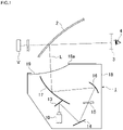
- Fig. 1 is an embodiment of the head-up display according to the present invention, and is an explanatory diagram particularly illustrating a configuration of an optical system.
- a head-up display 1 (hereinafter, referred to as a HUD 1) is arranged in the instrument panel of an automobile.
- the HUD 1 mainly includes a projection type display device 10, a first plane mirror 13, a second plane mirror 14, a screen 15, a first concave mirror 16, a second concave mirror 17, and a case 18.
- the HUD 1 reflects display light L representing a display image displayed by the projection type display device 10 by the first and second plane mirrors 13 and 14 and the first and second concave mirrors 16 and 17, which constitute a relay optical system, and irradiates the display light L to a front glass 2 of the automobile, which is an example of the transmission reflection part.
- a viewer (mainly the driver) can place a viewpoint 4 in an eyebox 3 which is an image visible area generated by the HUD 1, thereby superimposing the viewpoint 4 on a scene (real view) in front of the vehicle to visually recognize a virtual image V of a display image.
- the projection type display device 10 (display device 10) generates display light L related to the display image.
- the details of the display device 10 will be described later.
- the first plane mirror 13 reflects the display light L generated and emitted by the display device 10.
- the second plane mirror 14 further reflects the display light L reflected by the first plane mirror 13.
- the screen 15 receives the display light L reflected by the second plane mirror 14 and displays an image (real image).
- the first concave mirror 16 reflects the display light L emitted from the screen 15.
- the second concave mirror 17 reflects the display light L reflected by the first concave mirror 16 toward the front glass 2.
- the case 18 houses the display device 10, first and second plane mirrors 13 and 14, screen 15, and first and second concave mirrors 16 and 17.
- the case 18 has an opening 18a at a portion facing the front glass 2.
- the opening 18a is covered with a translucent cover 19 having translucency.
- the display light L reflected by the second concave mirror 17 is transmitted through the translucent cover 19 and emitted from the HUD 1.
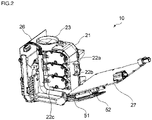
- Fig. 2 is a configuration diagram of the display device 10.
- Fig. 3 is an explanatory diagram illustrating the configuration of the optical system of the display device 10.
- the projection type display device 10 includes a housing 21, an LED substrate 22, an optical member 23, a light modulation element 24, a light modulation element control substrate 26, and a main control substrate 27.
- the housing 21 houses the optical member 23.
- the housing 21 has a structure for attaching the light modulation element 24 and each of the substrates 22, 26, and 27.
- the housing 21 includes a plurality of misassembly prevention protrusions 31a, 31b, and 31c (housing-side attachment parts) (see Fig. 5 ) for attaching the LED substrate 22.
- the LED (Light Emitting Diode) substrate 22 includes a first substrate 22a, a second substrate 22b, and a third substrate 22c, and different light sources are mounted.
- a red light source 62a that emits a red light ray R is implemented.
- a green light source 62b that emits a green light ray G is implemented.
- a blue light source 62c that emits a blue light ray B is implemented.
- the first to third substrates 22a, 22b, and 22c are not distinguished, they are simply referred to as the LED substrate 22.
- the red light source 62a, green light source 62b, and blue light source 62c are not distinguished, they are simply referred to as a light source 62.
- the details of the LED substrate 22 will be described later.
- the optical member 23 includes a mirror 41, dichroic mirrors 42 and 43, a reflecting mirror 44, a convex lens 45, a prism 46, and a projection lens 47.
- the red light ray R emitted from the red light source 62a is reflected by the mirror 41 and transmitted through the dichroic mirrors 42 and 43.
- the green light ray G emitted from the green light source 62b is reflected by the dichroic mirror 42 and transmitted through the dichroic mirror 43.
- the blue light ray B emitted from the blue light source 62c is reflected by the dichroic mirror 43.
- These rays R, G, and B are reflected by the reflecting mirror 44, distributed by the convex lens 45, and transmitted through the prism 46.
- the transmitted light rays R, G, and B are converted into the display light L by the light modulation element 24.
- the display light L is reflected by the prism 46, transmitted through the projection lens 47, and projected (emitted).
- the light modulation element 24 is, for example, a reflective display element such as a DMD (Digital Mirror Device) or an LCOS (Liquid Crystal On Silicon).
- a reflective display element such as a DMD (Digital Mirror Device) or an LCOS (Liquid Crystal On Silicon).
- the light modulation element control substrate 26 is connected to the light modulation element 24 and controls the light modulation element 24.
- the main control substrate 27 is connected to the LED substrate 22 by a wiring 51 and controls the LED substrate 22.
- the main control substrate 27 is connected to the light modulation element control substrate 26 by a wiring 52 and controls the light modulation element control substrate 26.
- Fig. 4 is a configuration diagram of the LED substrate 22 of the display device 10.
- the LED substrate (circuit substrate) 22 is a glass epoxy circuit substrate using for its base member, for example, FR4 (Flame Retardant Type 4).
- the LED substrate 22 is substantially rectangular (quadrangular) and includes misassembly prevention notches 55 (55a, 55b, and 55c) (substrate-side attachment part) and notches 56 for screwing (56a, 56b, and 56c).
- the misassembly prevention notches 55 are used when positioned in the housing 21 and are paired with the misassembly prevention protrusions 31a, 31b, and 31c of the housing 21.
- the notches 56 (56a, 56b, and 56c) for screwing are used when screwed to the housing 21 and paired with screw holes (not illustrated) of the housing 21.
- Fig. 5 is an enlarged view for explaining the attachment structure of the LED substrate 22 and the housing 21.
- the LED substrate 22 is fixed to an attachment wall 32 of the housing 21 with a screw 35 after positioning.
- the misassembly prevention notches 55a, 55b, and 55c of the first to third substrates 22a, 22b, and 22c are provided at different positions on one side 57a, 57b, and 57c of the rectangle, respectively.
- the misassembly prevention protrusions 31a, 31b, and 31c of the housing 21 are provided at different positions corresponding to the positions of these misassembly prevention notches 55a, 55b, and 55c.
- a pair of the protrusion 31a and notch 55a, a pair of the protrusion 31b and notch 55b, and a pair of the protrusion 31c and notch 55c are provided at different positions from one another. This prevents the LED substrate 22 from fitting if mounted in a wrong position. Therefore, it is possible to prevent the LED substrate 22 from being erroneously attached to the housing 21.
- the LED substrate 22 includes a heat dissipation plate 61, a light source 62, a thermistor 63, and a connector 64.
- the heat dissipation plate 61 is substantially square (quadrangular) in a plan view and radiates heat of the light source 62.
- the heat dissipation plate 61 includes a material having good heat conductivity and insulating properties, for example, aluminum nitride.
- the heat dissipation plate 61 preferably includes a material same as the material of the base member 71 of the light source 62 in view of thermal properties and the temperature detection by the thermistor 63.
- Fig. 6 is a cross-sectional view along the thickness direction of the LED substrate 22.
- the heat dissipation plate 61 is fixed to an opening 72 provided in the base member 71 with an adhesive 68.
- the adhesive 68 is, for example, an epoxy resin. That is, the heat dissipation plate 61 is embedded in the inner layer of the LED substrate 22.
- the light source 62 is substantially quadrangular in a plan view and is provided on the heat dissipation plate 61.
- the light source 62 is an SMD (Surface Mount Device) type LED (Light Emitting Diode), and includes an LED element 74 and a base plate 75.
- the base member 75 includes, for example, aluminum nitride (AlN).
- the thermistor 63 is provided on the heat dissipation plate 61, and detects a temperature. Information on the temperature of the heat dissipation plate 61 detected by the thermistor 63 is output to the main control substrate 27 as the temperature of the light source 62, and is used for controlling the light source 62 and the like.
- the connector 64 includes terminals 81a to 81d.
- the connector 64 connects the LED substrate 22 to a power supply (not illustrated) via a wiring 65a at the terminal 81a, thereby supplying power to the light source 62.
- the connector 64 connects the light source 62 to the ground (not illustrated) via a wiring 65b at the terminal 81b.
- the connector 64 connects the thermistor 63 and the power supply (not illustrated) via a wiring 65c at the terminal 81c, thereby supplying power to the thermistor 63.
- the connector 64 connects the thermistor 63 to the main control substrate 27 via a wiring 65d at the terminal 81d, thereby supplying a signal output from the thermistor 63 to the main control substrate 27.
- the terminals 81a and 81b are arranged outside.
- the terminals 81c and 81d are arranged inside.
- the light source 62 is arranged substantially at the center on the heat dissipation plate 61. With this, the heat generated by the light source 62 is radiated to the LED substrate 22 via the heat dissipation plate 61, and the heat radiation performance for heat generated by the light source is enhanced.
- the heat dissipation plate 61 is arranged in such a manner that a corner 91 of the heat dissipation plate 61 is rotated by approximately 45 degrees with respect to a corner 92 of the LED substrate 22. In addition, the heat dissipation plate 61 is arranged in such a manner that the corner 91 of the heat dissipation plate 61 is rotated by approximately 45 degrees with respect to a corner 93 of the light source 62.
- the heat dissipation plate 61, LED substrate 22, and light source 62 have a quadrangular shape having two orthogonal sides, orthogonal axes Xh and Yh that define the directions of the two orthogonal sides of the heat dissipation plate 61 are rotated by approximately 45 degrees with respect to orthogonal axes Xs,l and Ys,l that define the directions of the two orthogonal sides of the LED substrate 22 and the light source 62.
- the thermistor 63 is arranged on a straight line connecting the connector 64 and the light source 62.
- the wirings 65a to 65d can be short and simply arranged in combination with the arrangement of the terminals 81a to 81d.
- the arrangement of the wirings 65a to 65d can increase the heat radiating area of the heat dissipation plate 61 and is also preferable from the viewpoint of heat radiation.
- the heat dissipation plate 61 and the base member 75 are made of the same material. If the heat dissipation plate 61 and base member75 are not made of the same material, when they expand and contract by a temperature change due to a difference in thermal expansion coefficients, a load may be applied between the heat dissipation plate 61 and the base member 75, and a solder joint connecting the light source 62 and the wirings 65a and 65b may be broken, resulting in poor connection. Therefore, the use of the same material for the heat dissipation plate 61 and the base member 75 can prevent poor connection due to soldering crack.
- the heat dissipation plate 61 and the base member 75 are not limited to aluminum nitride (AlN).
- the base member 75 may be selected from aluminum (Al), gallium nitride (GaN), or the like. It is preferable that the difference between the thermal expansion coefficients of the heat dissipation plate 61 and the base member 75 is less than 1 (10 ⁇ -6/K), and it is preferable that the heat dissipation plate 61 and the base member 75 are made of the same material having no difference in the thermal expansion coefficients as an optimal material.
- the arrangement of the terminals 81a to 81d and the wirings 65a to 65d is not limited to this.
- the wiring 65a and wiring 65b side by side there is an advantage that the influence of electromagnetic waves can be canceled out.
Landscapes
- Physics & Mathematics (AREA)
- Engineering & Computer Science (AREA)
- General Physics & Mathematics (AREA)
- Optics & Photonics (AREA)
- Chemical & Material Sciences (AREA)
- Combustion & Propulsion (AREA)
- Transportation (AREA)
- Mechanical Engineering (AREA)
- Multimedia (AREA)
- Signal Processing (AREA)
- Instrument Panels (AREA)
Description
- The present invention relates to a head-up display mounted on a vehicle or the like.
- A head-up display is mounted on a vehicle and displays a virtual image of various information such as information necessary for driving, to a driver via a transmission reflection part such as a front glass. This allows the head-up display to display information (image), superimposing same on the scene in front of the vehicle. The driver can grasp necessary information without having to move a large line of sight while driving.
- The image is generated by, for example, a projection type display device. This projection type display device includes a substrate on which a light source is mounted. Since the light source is a heating element, various heat radiation measures have been taken for the substrate and a housing (for example, see Patent Document 1).
- Patent Document 1:
Japanese Unexamined Patent Application Publication No. 2016-218259 -
US7,034,778 B1 discloses a color head-up display, in particular for a vehicle, in which the light from a light source is transmitted through an at least partially light-transmitting display and can be projected onto a windshield, a multiplicity of red, blue and green light-emitting diodes are arranged without packaging on a common support, and that a heat-dissipating device for cooling the light-emitting diodes is present. -
JP2000031546 (A -
JP2010003968 (A - Today, light sources are required to have high brightness in order to enhance the visibility of displayed images. Consequently, the amount of heat generated by the light sources is increasing, and further heat radiation measures are required.
- The present invention has been made in view of such circumstances, and it is an object of the present invention to provide a head-up display having excellent heat radiation performance for heat generated by a light source.
- In order to solve the above-mentioned problem, the head-up display according to the present disclosure is a head-up display for irradiating display light of a display image projected by a display device to a transmission reflection part on a vehicle to allow a viewer to visually recognize a virtual image of the display image, and the display device includes a circuit substrate including a heat dissipation plate in an inner layer and a light source provided on the heat dissipation plate, as claimed hereinafter.
- The head-up display according to the present invention has excellent heat radiation performance for heat generated by a light source.
-
-
Fig. 1 is an embodiment of a head-up display according to the present invention, and is an explanatory diagram particularly illustrating a configuration of an optical system. -
Fig. 2 is a configuration diagram of a projection type display device. -
Fig. 3 is an explanatory diagram illustrating a configuration of an optical system of the projection type display device. -
Fig. 4 is a configuration diagram of an LED substrate of the projection type display device. -
Fig. 5 is an enlarged view for explaining an attachment structure of the LED substrate and a housing. -
Fig. 6 is a cross-sectional view along the thickness direction of the LED substrate. - An embodiment of the head-up display according to the present invention will be described with reference to the accompanying drawings. The head-up display according to the present invention is mounted on a vehicle such as an automobile, for example. In this embodiment, this is explained with the use of an example in which the head-up display according to the present invention is mounted on an automobile.
-
Fig. 1 is an embodiment of the head-up display according to the present invention, and is an explanatory diagram particularly illustrating a configuration of an optical system. - A head-up display 1 (hereinafter, referred to as a HUD 1) is arranged in the instrument panel of an automobile. The
HUD 1 mainly includes a projectiontype display device 10, afirst plane mirror 13, asecond plane mirror 14, ascreen 15, a firstconcave mirror 16, a secondconcave mirror 17, and acase 18. TheHUD 1 reflects display light L representing a display image displayed by the projectiontype display device 10 by the first andsecond plane mirrors concave mirrors front glass 2 of the automobile, which is an example of the transmission reflection part. A viewer (mainly the driver) can place aviewpoint 4 in aneyebox 3 which is an image visible area generated by theHUD 1, thereby superimposing theviewpoint 4 on a scene (real view) in front of the vehicle to visually recognize a virtual image V of a display image. - The projection type display device 10 (display device 10) generates display light L related to the display image. The details of the
display device 10 will be described later. Thefirst plane mirror 13 reflects the display light L generated and emitted by thedisplay device 10. Thesecond plane mirror 14 further reflects the display light L reflected by thefirst plane mirror 13. Thescreen 15 receives the display light L reflected by thesecond plane mirror 14 and displays an image (real image). The firstconcave mirror 16 reflects the display light L emitted from thescreen 15. The secondconcave mirror 17 reflects the display light L reflected by the firstconcave mirror 16 toward thefront glass 2. Thecase 18 houses thedisplay device 10, first andsecond plane mirrors screen 15, and first and secondconcave mirrors case 18 has an opening 18a at a portion facing thefront glass 2. The opening 18a is covered with atranslucent cover 19 having translucency. The display light L reflected by the secondconcave mirror 17 is transmitted through thetranslucent cover 19 and emitted from theHUD 1. -
Fig. 2 is a configuration diagram of thedisplay device 10. -
Fig. 3 is an explanatory diagram illustrating the configuration of the optical system of thedisplay device 10. - The projection
type display device 10 includes ahousing 21, anLED substrate 22, anoptical member 23, alight modulation element 24, a light modulationelement control substrate 26, and amain control substrate 27. - The
housing 21 houses theoptical member 23. Thehousing 21 has a structure for attaching thelight modulation element 24 and each of thesubstrates housing 21 includes a plurality ofmisassembly prevention protrusions Fig. 5 ) for attaching theLED substrate 22. - The LED (Light Emitting Diode)
substrate 22 includes afirst substrate 22a, asecond substrate 22b, and athird substrate 22c, and different light sources are mounted. In thefirst substrate 22a, ared light source 62a that emits a red light ray R is implemented. In thesecond substrate 22b, agreen light source 62b that emits a green light ray G is implemented. In thethird substrate 22c, ablue light source 62c that emits a blue light ray B is implemented. In the following description, when the first tothird substrates LED substrate 22. In addition, when thered light source 62a,green light source 62b, andblue light source 62c are not distinguished, they are simply referred to as alight source 62. The details of theLED substrate 22 will be described later. - As illustrated in
Fig. 3 , theoptical member 23 includes amirror 41,dichroic mirrors mirror 44, aconvex lens 45, aprism 46, and aprojection lens 47. - The red light ray R emitted from the
red light source 62a is reflected by themirror 41 and transmitted through thedichroic mirrors green light source 62b is reflected by thedichroic mirror 42 and transmitted through thedichroic mirror 43. The blue light ray B emitted from the bluelight source 62c is reflected by thedichroic mirror 43. These rays R, G, and B are reflected by the reflectingmirror 44, distributed by theconvex lens 45, and transmitted through theprism 46. The transmitted light rays R, G, and B are converted into the display light L by thelight modulation element 24. The display light L is reflected by theprism 46, transmitted through theprojection lens 47, and projected (emitted). - The
light modulation element 24 is, for example, a reflective display element such as a DMD (Digital Mirror Device) or an LCOS (Liquid Crystal On Silicon). - The light modulation
element control substrate 26 is connected to thelight modulation element 24 and controls thelight modulation element 24. - The
main control substrate 27 is connected to theLED substrate 22 by awiring 51 and controls theLED substrate 22. In addition, themain control substrate 27 is connected to the light modulationelement control substrate 26 by awiring 52 and controls the light modulationelement control substrate 26. -
Fig. 4 is a configuration diagram of theLED substrate 22 of thedisplay device 10. - The LED substrate (circuit substrate) 22 is a glass epoxy circuit substrate using for its base member, for example, FR4 (Flame Retardant Type 4). The
LED substrate 22 is substantially rectangular (quadrangular) and includes misassembly prevention notches 55 (55a, 55b, and 55c) (substrate-side attachment part) andnotches 56 for screwing (56a, 56b, and 56c). Themisassembly prevention notches 55 are used when positioned in thehousing 21 and are paired with themisassembly prevention protrusions housing 21. The notches 56 (56a, 56b, and 56c) for screwing are used when screwed to thehousing 21 and paired with screw holes (not illustrated) of thehousing 21. - Here,
Fig. 5 is an enlarged view for explaining the attachment structure of theLED substrate 22 and thehousing 21. - The
LED substrate 22 is fixed to anattachment wall 32 of thehousing 21 with ascrew 35 after positioning. Themisassembly prevention notches third substrates side misassembly prevention protrusions housing 21 are provided at different positions corresponding to the positions of thesemisassembly prevention notches protrusion 31a andnotch 55a, a pair of theprotrusion 31b andnotch 55b, and a pair of theprotrusion 31c andnotch 55c are provided at different positions from one another. This prevents theLED substrate 22 from fitting if mounted in a wrong position. Therefore, it is possible to prevent theLED substrate 22 from being erroneously attached to thehousing 21. - As illustrated in
Fig. 4 , theLED substrate 22 includes aheat dissipation plate 61, alight source 62, athermistor 63, and aconnector 64. - The
heat dissipation plate 61 is substantially square (quadrangular) in a plan view and radiates heat of thelight source 62. Theheat dissipation plate 61 includes a material having good heat conductivity and insulating properties, for example, aluminum nitride. Theheat dissipation plate 61 preferably includes a material same as the material of thebase member 71 of thelight source 62 in view of thermal properties and the temperature detection by thethermistor 63. Here,Fig. 6 is a cross-sectional view along the thickness direction of theLED substrate 22. Theheat dissipation plate 61 is fixed to anopening 72 provided in thebase member 71 with an adhesive 68. The adhesive 68 is, for example, an epoxy resin. That is, theheat dissipation plate 61 is embedded in the inner layer of theLED substrate 22. - The
light source 62 is substantially quadrangular in a plan view and is provided on theheat dissipation plate 61. Thelight source 62 is an SMD (Surface Mount Device) type LED (Light Emitting Diode), and includes anLED element 74 and abase plate 75. Thebase member 75 includes, for example, aluminum nitride (AlN). - The
thermistor 63 is provided on theheat dissipation plate 61, and detects a temperature. Information on the temperature of theheat dissipation plate 61 detected by thethermistor 63 is output to themain control substrate 27 as the temperature of thelight source 62, and is used for controlling thelight source 62 and the like. - The
connector 64 includesterminals 81a to 81d. Theconnector 64 connects theLED substrate 22 to a power supply (not illustrated) via awiring 65a at the terminal 81a, thereby supplying power to thelight source 62. Theconnector 64 connects thelight source 62 to the ground (not illustrated) via awiring 65b at the terminal 81b. Theconnector 64 connects thethermistor 63 and the power supply (not illustrated) via awiring 65c at the terminal 81c, thereby supplying power to thethermistor 63. Theconnector 64 connects thethermistor 63 to themain control substrate 27 via awiring 65d at the terminal 81d, thereby supplying a signal output from thethermistor 63 to themain control substrate 27. Of theterminals 81a to 81d, theterminals terminals 81a to 81d, theterminals - Next, the arrangement of each component on the
LED substrate 22 will be described. - As illustrated in
Fig. 4 , thelight source 62 is arranged substantially at the center on theheat dissipation plate 61. With this, the heat generated by thelight source 62 is radiated to theLED substrate 22 via theheat dissipation plate 61, and the heat radiation performance for heat generated by the light source is enhanced. - In addition, the
heat dissipation plate 61 is arranged in such a manner that acorner 91 of theheat dissipation plate 61 is rotated by approximately 45 degrees with respect to acorner 92 of theLED substrate 22. In addition, theheat dissipation plate 61 is arranged in such a manner that thecorner 91 of theheat dissipation plate 61 is rotated by approximately 45 degrees with respect to acorner 93 of thelight source 62. That is, if theheat dissipation plate 61,LED substrate 22, andlight source 62 have a quadrangular shape having two orthogonal sides, orthogonal axes Xh and Yh that define the directions of the two orthogonal sides of theheat dissipation plate 61 are rotated by approximately 45 degrees with respect to orthogonal axes Xs,l and Ys,l that define the directions of the two orthogonal sides of theLED substrate 22 and thelight source 62. - This allows a wider margin to be formed on the
heat dissipation plate 61 when thelight source 62 is arranged at the center of theheat dissipation plate 61 compared to when each of thecorners heat dissipation plate 61 and thelight source 62 are not rotated and arranged, and therefore thethermistor 63 can be arranged in this margin. In addition, since thelight source 62 and thethermistor 63 can be arranged on theheat dissipation plate 61, the temperature of thelight source 62 can be accurately detected by thethermistor 63. - In addition, the
thermistor 63 is arranged on a straight line connecting theconnector 64 and thelight source 62. With this, thewirings 65a to 65d can be short and simply arranged in combination with the arrangement of theterminals 81a to 81d. Moreover, in this manner, the arrangement of thewirings 65a to 65d can increase the heat radiating area of theheat dissipation plate 61 and is also preferable from the viewpoint of heat radiation. - In addition, the
heat dissipation plate 61 and thebase member 75 are made of the same material. If theheat dissipation plate 61 and base member75 are not made of the same material, when they expand and contract by a temperature change due to a difference in thermal expansion coefficients, a load may be applied between theheat dissipation plate 61 and thebase member 75, and a solder joint connecting thelight source 62 and thewirings heat dissipation plate 61 and thebase member 75 can prevent poor connection due to soldering crack. - While several embodiments of the present invention have been described, these embodiments are provided by way of example of the invention which is defined by the appended claims.
- For example, the
heat dissipation plate 61 and thebase member 75 are not limited to aluminum nitride (AlN). Thebase member 75 may be selected from aluminum (Al), gallium nitride (GaN), or the like. It is preferable that the difference between the thermal expansion coefficients of theheat dissipation plate 61 and thebase member 75 is less than 1 (10^-6/K), and it is preferable that theheat dissipation plate 61 and thebase member 75 are made of the same material having no difference in the thermal expansion coefficients as an optimal material. - In addition, the arrangement of the
terminals 81a to 81d and thewirings 65a to 65d is not limited to this. For example, by arranging thewiring 65a andwiring 65b side by side, there is an advantage that the influence of electromagnetic waves can be canceled out. -
- 1
- head-up display (HUD)
- 2
- front glass
- 3
- eyebox
- 4
- viewpoint
- 10
- projection type display device (display device)
- 13
- first plane mirror
- 14
- second plane mirror
- 15
- screen
- 16
- first concave mirror
- 17
- second concave mirror
- 18
- case
- 18a
- opening
- 19
- translucent cover
- 21
- housing
- 22
- LED substrate (circuit substrate)
- 22a
- first substrate
- 22b
- second substrate
- 22c
- third substrate
- 23
- optical member
- 24
- light modulation element
- 26
- light modulation element control substrate
- 27
- main control substrate
- 31a, 31b, 31c
- misassembly prevention protrusions
- 32
- attachment wall
- 41
- mirror
- 42, 43
- dichroic mirrors
- 44
- reflecting mirror
- 45
- convex lens
- 46
- prism
- 47
- projection lens
- 51, 52
- wirings
- 55, 55a, 55b, 55c
- misassembly prevention protrusions
- 61
- heat dissipation plate
- 62
- light source
- 62a
- red light source
- 62b
- green light source
- 62c
- blue light source
- 63
- thermistor
- 64
- connector
- 65a, 65b, 65c, 65d
- wirings
- 68
- adhesive
- 71, 75
- base members
- 72
- opening
- 74
- LED element
- 81a, 81b, 81c, 81d
- terminals
- 91, 92, 93
- corners
Claims (4)
- A head-up display (1) for irradiating display light (L) of a display image projected by a display device to a transmission reflection part (2) on a vehicle to allow a viewer to visually recognize a virtual image (V) of the display image,wherein the display device includes a circuit substrate (22) including a heat dissipation plate (61) in an inner layer and a light source (62) provided on the heat dissipation plate;wherein the heat dissipation plate includes a rectangular heat dissipation plate having a corner (91), the light source includes a rectangular light source having a corner (93);characterized in that the circuit substrate includes a quadrangular shape having a corner, andwherein the heat dissipation plate is arranged in such a manner that the corner of the heat dissipation plate is rotated by approximately 45 degrees with respect to the corner of the light source and is rotated by approximately 45 degrees with respect to the corner of the circuit substrate.
- The head-up display according to claim 1, further comprising a thermistor (63) provided on the heat dissipation plate and configured to detect a temperature of the light source.
- The head-up display according to any one of claims 1 to 2,wherein the light source includes a base member (71), andwherein the heat dissipation plate includes a material same as a material of the base member.
- The head-up display according to any one of claims 1 to 3,wherein the display device includes a plurality of the circuit substrates on which different light sources are mounted, and a housing (21) to which the plurality of circuit substrates are attached,wherein the housing includes a plurality of housing-side attachment parts (31) for attaching the plurality of circuit substrates, the plurality of circuit substrates include a plurality of substrate-side attachment parts (55) that are paired with the plurality of housing-side attachment parts, respectively, andwherein pairs of the plurality of housing-side attachment parts and the plurality of substrate-side attachment parts are provided at different positions, respectively.
Applications Claiming Priority (2)
| Application Number | Priority Date | Filing Date | Title |
|---|---|---|---|
| JP2017186079 | 2017-09-27 | ||
| PCT/JP2018/035408 WO2019065613A1 (en) | 2017-09-27 | 2018-09-25 | Head-up display |
Publications (3)
| Publication Number | Publication Date |
|---|---|
| EP3689661A1 EP3689661A1 (en) | 2020-08-05 |
| EP3689661A4 EP3689661A4 (en) | 2021-06-09 |
| EP3689661B1 true EP3689661B1 (en) | 2022-08-17 |
Family
ID=65900878
Family Applications (1)
| Application Number | Title | Priority Date | Filing Date |
|---|---|---|---|
| EP18863052.9A Active EP3689661B1 (en) | 2017-09-27 | 2018-09-25 | Head-up display |
Country Status (5)
| Country | Link |
|---|---|
| US (1) | US11061229B2 (en) |
| EP (1) | EP3689661B1 (en) |
| JP (1) | JP7136113B2 (en) |
| CN (1) | CN111148648B (en) |
| WO (1) | WO2019065613A1 (en) |
Families Citing this family (2)
| Publication number | Priority date | Publication date | Assignee | Title |
|---|---|---|---|---|
| JP7474028B2 (en) | 2019-02-22 | 2024-04-24 | マクセル株式会社 | Head-up display |
| DE102021130460A1 (en) * | 2021-11-22 | 2023-05-25 | Valeo Schalter Und Sensoren Gmbh | Image signal generating device, head-up display and method of assembling a head-up display |
Family Cites Families (16)
| Publication number | Priority date | Publication date | Assignee | Title |
|---|---|---|---|---|
| US3577137A (en) * | 1968-12-31 | 1971-05-04 | Texas Instruments Inc | Temperature compensated electronic display |
| JP2000031546A (en) * | 1998-07-08 | 2000-01-28 | Mitsubishi Electric Corp | LED assembly module |
| DE10016817A1 (en) * | 2000-04-05 | 2001-10-18 | Mannesmann Vdo Ag | Color head-up display, especially for a vehicle |
| JP4345052B2 (en) * | 2003-06-30 | 2009-10-14 | オプトレックス株式会社 | Liquid crystal display |
| JP2005181915A (en) * | 2003-12-24 | 2005-07-07 | Nippon Seiki Co Ltd | Vehicle display device |
| US20050254208A1 (en) * | 2004-05-17 | 2005-11-17 | Belady Christian L | Air flow direction neutral heat transfer device |
| JP2006011168A (en) * | 2004-06-28 | 2006-01-12 | Nippon Seiki Co Ltd | Head-up display device for vehicle |
| JPWO2008132941A1 (en) * | 2007-04-13 | 2010-07-22 | 昭和電工株式会社 | Light emitting device and display device |
| JP5235105B2 (en) * | 2008-06-23 | 2013-07-10 | パナソニック株式会社 | Light emitting device |
| JP5793639B2 (en) * | 2010-04-20 | 2015-10-14 | パナソニックIpマネジメント株式会社 | See-through display and head-up display |
| JP2014194500A (en) * | 2013-03-29 | 2014-10-09 | Funai Electric Co Ltd | Projector and head-up display device |
| JP2015065391A (en) | 2013-09-26 | 2015-04-09 | アルプス電気株式会社 | Video display device |
| KR20170063647A (en) * | 2014-09-24 | 2017-06-08 | 닛폰 세이키 가부시키가이샤 | Head-up display device |
| FR3029353B1 (en) * | 2014-11-28 | 2016-12-23 | Valeo Comfort & Driving Assistance | BACKLIGHT DEVICE, IN PARTICULAR FOR HIGH HEAD DISPLAY AND HIGH HEAD DISPLAY FOR MOTOR VEHICLE |
| US20200240717A1 (en) * | 2015-02-27 | 2020-07-30 | Laird Thermal Systems, Inc. | Heat Sinks Including Heat Pipes And Related Methods |
| JP6604033B2 (en) * | 2015-05-20 | 2019-11-13 | 日本精機株式会社 | Projection display |
-
2018
- 2018-09-25 US US16/649,575 patent/US11061229B2/en active Active
- 2018-09-25 EP EP18863052.9A patent/EP3689661B1/en active Active
- 2018-09-25 WO PCT/JP2018/035408 patent/WO2019065613A1/en not_active Ceased
- 2018-09-25 CN CN201880062671.7A patent/CN111148648B/en active Active
- 2018-09-25 JP JP2019545123A patent/JP7136113B2/en active Active
Also Published As
| Publication number | Publication date |
|---|---|
| WO2019065613A1 (en) | 2019-04-04 |
| US20200285054A1 (en) | 2020-09-10 |
| US11061229B2 (en) | 2021-07-13 |
| JP7136113B2 (en) | 2022-09-13 |
| CN111148648A (en) | 2020-05-12 |
| EP3689661A4 (en) | 2021-06-09 |
| EP3689661A1 (en) | 2020-08-05 |
| JPWO2019065613A1 (en) | 2020-11-19 |
| CN111148648B (en) | 2023-06-30 |
Similar Documents
| Publication | Publication Date | Title |
|---|---|---|
| JP6004706B2 (en) | Display device and head-up display system provided with the same | |
| JP4706206B2 (en) | Heat dissipation device and display device | |
| US10612764B2 (en) | Illumination unit and display apparatus | |
| US20120300486A1 (en) | Vehicle back light unit and vehicle display system | |
| CN107257936A (en) | Backlighting arrangement, it is particularly used for head-up display, and the head-up display for motor vehicles | |
| EP4163700B1 (en) | Vehicular display device | |
| CN106090842A (en) | For luminescence, it is particularly useful for producing the device of image | |
| JP2020134588A (en) | Virtual image display device | |
| TWI601904B (en) | Lighting unit and display device using the same | |
| JP2007086387A (en) | On-vehicle display device | |
| JP4650075B2 (en) | Light emitting unit heat dissipation device, backlight device, and image display device | |
| US11061229B2 (en) | Head-up display | |
| JP2015138114A (en) | Scanning display device, and projection device | |
| TWI525370B (en) | Liquid crystal display device | |
| JP2004006096A (en) | Lighting equipment | |
| CN109844605A (en) | Video generation device and relevant head-up display including thermally contacting area | |
| US20170199449A1 (en) | Projection-type display device and heat dissipation method | |
| JP7176528B2 (en) | Composite substrate | |
| US8591043B2 (en) | Light modulation device and projector | |
| US20200387030A1 (en) | Image generating device and associated head-up display | |
| US11874548B2 (en) | Image forming panel device and projector | |
| JP2019133048A (en) | Liquid crystal display unit for vehicle and head-up display device | |
| WO2024161860A1 (en) | Head-up display device | |
| WO2026103845A1 (en) | Image source assembly, and head-up display device | |
| CN120274232A (en) | Imaging device, projection device, lamp device, display device, and vehicle |
Legal Events
| Date | Code | Title | Description |
|---|---|---|---|
| STAA | Information on the status of an ep patent application or granted ep patent |
Free format text: STATUS: THE INTERNATIONAL PUBLICATION HAS BEEN MADE |
|
| PUAI | Public reference made under article 153(3) epc to a published international application that has entered the european phase |
Free format text: ORIGINAL CODE: 0009012 |
|
| STAA | Information on the status of an ep patent application or granted ep patent |
Free format text: STATUS: REQUEST FOR EXAMINATION WAS MADE |
|
| 17P | Request for examination filed |
Effective date: 20200316 |
|
| AK | Designated contracting states |
Kind code of ref document: A1 Designated state(s): AL AT BE BG CH CY CZ DE DK EE ES FI FR GB GR HR HU IE IS IT LI LT LU LV MC MK MT NL NO PL PT RO RS SE SI SK SM TR |
|
| AX | Request for extension of the european patent |
Extension state: BA ME |
|
| DAV | Request for validation of the european patent (deleted) | ||
| DAX | Request for extension of the european patent (deleted) | ||
| A4 | Supplementary search report drawn up and despatched |
Effective date: 20210507 |
|
| RIC1 | Information provided on ipc code assigned before grant |
Ipc: B60K 35/00 20060101AFI20210430BHEP Ipc: G02B 27/01 20060101ALI20210430BHEP Ipc: G03B 21/16 20060101ALI20210430BHEP Ipc: H04N 5/64 20060101ALI20210430BHEP Ipc: F21V 29/503 20150101ALI20210430BHEP Ipc: F21V 29/70 20150101ALI20210430BHEP |
|
| GRAP | Despatch of communication of intention to grant a patent |
Free format text: ORIGINAL CODE: EPIDOSNIGR1 |
|
| STAA | Information on the status of an ep patent application or granted ep patent |
Free format text: STATUS: GRANT OF PATENT IS INTENDED |
|
| INTG | Intention to grant announced |
Effective date: 20220407 |
|
| GRAS | Grant fee paid |
Free format text: ORIGINAL CODE: EPIDOSNIGR3 |
|
| GRAA | (expected) grant |
Free format text: ORIGINAL CODE: 0009210 |
|
| STAA | Information on the status of an ep patent application or granted ep patent |
Free format text: STATUS: THE PATENT HAS BEEN GRANTED |
|
| AK | Designated contracting states |
Kind code of ref document: B1 Designated state(s): AL AT BE BG CH CY CZ DE DK EE ES FI FR GB GR HR HU IE IS IT LI LT LU LV MC MK MT NL NO PL PT RO RS SE SI SK SM TR |
|
| REG | Reference to a national code |
Ref country code: CH Ref legal event code: EP |
|
| REG | Reference to a national code |
Ref country code: DE Ref legal event code: R096 Ref document number: 602018039528 Country of ref document: DE |
|
| REG | Reference to a national code |
Ref country code: IE Ref legal event code: FG4D |
|
| REG | Reference to a national code |
Ref country code: AT Ref legal event code: REF Ref document number: 1511960 Country of ref document: AT Kind code of ref document: T Effective date: 20220915 |
|
| REG | Reference to a national code |
Ref country code: NL Ref legal event code: MP Effective date: 20220817 |
|
| REG | Reference to a national code |
Ref country code: LT Ref legal event code: MG9D |
|
| PG25 | Lapsed in a contracting state [announced via postgrant information from national office to epo] |
Ref country code: SE Free format text: LAPSE BECAUSE OF FAILURE TO SUBMIT A TRANSLATION OF THE DESCRIPTION OR TO PAY THE FEE WITHIN THE PRESCRIBED TIME-LIMIT Effective date: 20220817 Ref country code: RS Free format text: LAPSE BECAUSE OF FAILURE TO SUBMIT A TRANSLATION OF THE DESCRIPTION OR TO PAY THE FEE WITHIN THE PRESCRIBED TIME-LIMIT Effective date: 20220817 Ref country code: PT Free format text: LAPSE BECAUSE OF FAILURE TO SUBMIT A TRANSLATION OF THE DESCRIPTION OR TO PAY THE FEE WITHIN THE PRESCRIBED TIME-LIMIT Effective date: 20221219 Ref country code: NO Free format text: LAPSE BECAUSE OF FAILURE TO SUBMIT A TRANSLATION OF THE DESCRIPTION OR TO PAY THE FEE WITHIN THE PRESCRIBED TIME-LIMIT Effective date: 20221117 Ref country code: NL Free format text: LAPSE BECAUSE OF FAILURE TO SUBMIT A TRANSLATION OF THE DESCRIPTION OR TO PAY THE FEE WITHIN THE PRESCRIBED TIME-LIMIT Effective date: 20220817 Ref country code: LV Free format text: LAPSE BECAUSE OF FAILURE TO SUBMIT A TRANSLATION OF THE DESCRIPTION OR TO PAY THE FEE WITHIN THE PRESCRIBED TIME-LIMIT Effective date: 20220817 Ref country code: LT Free format text: LAPSE BECAUSE OF FAILURE TO SUBMIT A TRANSLATION OF THE DESCRIPTION OR TO PAY THE FEE WITHIN THE PRESCRIBED TIME-LIMIT Effective date: 20220817 Ref country code: FI Free format text: LAPSE BECAUSE OF FAILURE TO SUBMIT A TRANSLATION OF THE DESCRIPTION OR TO PAY THE FEE WITHIN THE PRESCRIBED TIME-LIMIT Effective date: 20220817 |
|
| REG | Reference to a national code |
Ref country code: AT Ref legal event code: MK05 Ref document number: 1511960 Country of ref document: AT Kind code of ref document: T Effective date: 20220817 |
|
| PG25 | Lapsed in a contracting state [announced via postgrant information from national office to epo] |
Ref country code: PL Free format text: LAPSE BECAUSE OF FAILURE TO SUBMIT A TRANSLATION OF THE DESCRIPTION OR TO PAY THE FEE WITHIN THE PRESCRIBED TIME-LIMIT Effective date: 20220817 Ref country code: IS Free format text: LAPSE BECAUSE OF FAILURE TO SUBMIT A TRANSLATION OF THE DESCRIPTION OR TO PAY THE FEE WITHIN THE PRESCRIBED TIME-LIMIT Effective date: 20221217 Ref country code: HR Free format text: LAPSE BECAUSE OF FAILURE TO SUBMIT A TRANSLATION OF THE DESCRIPTION OR TO PAY THE FEE WITHIN THE PRESCRIBED TIME-LIMIT Effective date: 20220817 Ref country code: GR Free format text: LAPSE BECAUSE OF FAILURE TO SUBMIT A TRANSLATION OF THE DESCRIPTION OR TO PAY THE FEE WITHIN THE PRESCRIBED TIME-LIMIT Effective date: 20221118 |
|
| PG25 | Lapsed in a contracting state [announced via postgrant information from national office to epo] |
Ref country code: SM Free format text: LAPSE BECAUSE OF FAILURE TO SUBMIT A TRANSLATION OF THE DESCRIPTION OR TO PAY THE FEE WITHIN THE PRESCRIBED TIME-LIMIT Effective date: 20220817 Ref country code: RO Free format text: LAPSE BECAUSE OF FAILURE TO SUBMIT A TRANSLATION OF THE DESCRIPTION OR TO PAY THE FEE WITHIN THE PRESCRIBED TIME-LIMIT Effective date: 20220817 Ref country code: ES Free format text: LAPSE BECAUSE OF FAILURE TO SUBMIT A TRANSLATION OF THE DESCRIPTION OR TO PAY THE FEE WITHIN THE PRESCRIBED TIME-LIMIT Effective date: 20220817 Ref country code: DK Free format text: LAPSE BECAUSE OF FAILURE TO SUBMIT A TRANSLATION OF THE DESCRIPTION OR TO PAY THE FEE WITHIN THE PRESCRIBED TIME-LIMIT Effective date: 20220817 Ref country code: CZ Free format text: LAPSE BECAUSE OF FAILURE TO SUBMIT A TRANSLATION OF THE DESCRIPTION OR TO PAY THE FEE WITHIN THE PRESCRIBED TIME-LIMIT Effective date: 20220817 Ref country code: AT Free format text: LAPSE BECAUSE OF FAILURE TO SUBMIT A TRANSLATION OF THE DESCRIPTION OR TO PAY THE FEE WITHIN THE PRESCRIBED TIME-LIMIT Effective date: 20220817 |
|
| REG | Reference to a national code |
Ref country code: CH Ref legal event code: PL |
|
| REG | Reference to a national code |
Ref country code: DE Ref legal event code: R097 Ref document number: 602018039528 Country of ref document: DE |
|
| REG | Reference to a national code |
Ref country code: BE Ref legal event code: MM Effective date: 20220930 |
|
| PG25 | Lapsed in a contracting state [announced via postgrant information from national office to epo] |
Ref country code: SK Free format text: LAPSE BECAUSE OF FAILURE TO SUBMIT A TRANSLATION OF THE DESCRIPTION OR TO PAY THE FEE WITHIN THE PRESCRIBED TIME-LIMIT Effective date: 20220817 Ref country code: MC Free format text: LAPSE BECAUSE OF FAILURE TO SUBMIT A TRANSLATION OF THE DESCRIPTION OR TO PAY THE FEE WITHIN THE PRESCRIBED TIME-LIMIT Effective date: 20220817 Ref country code: EE Free format text: LAPSE BECAUSE OF FAILURE TO SUBMIT A TRANSLATION OF THE DESCRIPTION OR TO PAY THE FEE WITHIN THE PRESCRIBED TIME-LIMIT Effective date: 20220817 |
|
| PLBE | No opposition filed within time limit |
Free format text: ORIGINAL CODE: 0009261 |
|
| STAA | Information on the status of an ep patent application or granted ep patent |
Free format text: STATUS: NO OPPOSITION FILED WITHIN TIME LIMIT |
|
| PG25 | Lapsed in a contracting state [announced via postgrant information from national office to epo] |
Ref country code: LU Free format text: LAPSE BECAUSE OF NON-PAYMENT OF DUE FEES Effective date: 20220925 Ref country code: AL Free format text: LAPSE BECAUSE OF FAILURE TO SUBMIT A TRANSLATION OF THE DESCRIPTION OR TO PAY THE FEE WITHIN THE PRESCRIBED TIME-LIMIT Effective date: 20220817 |
|
| 26N | No opposition filed |
Effective date: 20230519 |
|
| GBPC | Gb: european patent ceased through non-payment of renewal fee |
Effective date: 20221117 |
|
| PG25 | Lapsed in a contracting state [announced via postgrant information from national office to epo] |
Ref country code: LI Free format text: LAPSE BECAUSE OF NON-PAYMENT OF DUE FEES Effective date: 20220930 Ref country code: IE Free format text: LAPSE BECAUSE OF NON-PAYMENT OF DUE FEES Effective date: 20220925 Ref country code: FR Free format text: LAPSE BECAUSE OF NON-PAYMENT OF DUE FEES Effective date: 20221017 Ref country code: CH Free format text: LAPSE BECAUSE OF NON-PAYMENT OF DUE FEES Effective date: 20220930 |
|
| PG25 | Lapsed in a contracting state [announced via postgrant information from national office to epo] |
Ref country code: SI Free format text: LAPSE BECAUSE OF FAILURE TO SUBMIT A TRANSLATION OF THE DESCRIPTION OR TO PAY THE FEE WITHIN THE PRESCRIBED TIME-LIMIT Effective date: 20220817 |
|
| PG25 | Lapsed in a contracting state [announced via postgrant information from national office to epo] |
Ref country code: BE Free format text: LAPSE BECAUSE OF NON-PAYMENT OF DUE FEES Effective date: 20220930 |
|
| PG25 | Lapsed in a contracting state [announced via postgrant information from national office to epo] |
Ref country code: GB Free format text: LAPSE BECAUSE OF NON-PAYMENT OF DUE FEES Effective date: 20221117 |
|
| PG25 | Lapsed in a contracting state [announced via postgrant information from national office to epo] |
Ref country code: CY Free format text: LAPSE BECAUSE OF FAILURE TO SUBMIT A TRANSLATION OF THE DESCRIPTION OR TO PAY THE FEE WITHIN THE PRESCRIBED TIME-LIMIT Effective date: 20220817 |
|
| PG25 | Lapsed in a contracting state [announced via postgrant information from national office to epo] |
Ref country code: MK Free format text: LAPSE BECAUSE OF FAILURE TO SUBMIT A TRANSLATION OF THE DESCRIPTION OR TO PAY THE FEE WITHIN THE PRESCRIBED TIME-LIMIT Effective date: 20220817 Ref country code: IT Free format text: LAPSE BECAUSE OF FAILURE TO SUBMIT A TRANSLATION OF THE DESCRIPTION OR TO PAY THE FEE WITHIN THE PRESCRIBED TIME-LIMIT Effective date: 20220817 Ref country code: HU Free format text: LAPSE BECAUSE OF FAILURE TO SUBMIT A TRANSLATION OF THE DESCRIPTION OR TO PAY THE FEE WITHIN THE PRESCRIBED TIME-LIMIT; INVALID AB INITIO Effective date: 20180925 |
|
| PG25 | Lapsed in a contracting state [announced via postgrant information from national office to epo] |
Ref country code: BG Free format text: LAPSE BECAUSE OF FAILURE TO SUBMIT A TRANSLATION OF THE DESCRIPTION OR TO PAY THE FEE WITHIN THE PRESCRIBED TIME-LIMIT Effective date: 20220817 |
|
| PG25 | Lapsed in a contracting state [announced via postgrant information from national office to epo] |
Ref country code: MT Free format text: LAPSE BECAUSE OF FAILURE TO SUBMIT A TRANSLATION OF THE DESCRIPTION OR TO PAY THE FEE WITHIN THE PRESCRIBED TIME-LIMIT Effective date: 20220817 |
|
| PGFP | Annual fee paid to national office [announced via postgrant information from national office to epo] |
Ref country code: DE Payment date: 20250730 Year of fee payment: 8 |
|
| PG25 | Lapsed in a contracting state [announced via postgrant information from national office to epo] |
Ref country code: TR Free format text: LAPSE BECAUSE OF FAILURE TO SUBMIT A TRANSLATION OF THE DESCRIPTION OR TO PAY THE FEE WITHIN THE PRESCRIBED TIME-LIMIT Effective date: 20220817 |