EP3686937A1 - Semiconductor apparatus for detecting or oscillating electromagnetic waves, imaging system, and moving object - Google Patents
Semiconductor apparatus for detecting or oscillating electromagnetic waves, imaging system, and moving object Download PDFInfo
- Publication number
- EP3686937A1 EP3686937A1 EP20153800.6A EP20153800A EP3686937A1 EP 3686937 A1 EP3686937 A1 EP 3686937A1 EP 20153800 A EP20153800 A EP 20153800A EP 3686937 A1 EP3686937 A1 EP 3686937A1
- Authority
- EP
- European Patent Office
- Prior art keywords
- waves
- terahertz
- electromagnetic waves
- wavelength
- semiconductor apparatus
- Prior art date
- Legal status (The legal status is an assumption and is not a legal conclusion. Google has not performed a legal analysis and makes no representation as to the accuracy of the status listed.)
- Granted
Links
Images


Classifications
-
- G—PHYSICS
- G01—MEASURING; TESTING
- G01S—RADIO DIRECTION-FINDING; RADIO NAVIGATION; DETERMINING DISTANCE OR VELOCITY BY USE OF RADIO WAVES; LOCATING OR PRESENCE-DETECTING BY USE OF THE REFLECTION OR RERADIATION OF RADIO WAVES; ANALOGOUS ARRANGEMENTS USING OTHER WAVES
- G01S17/00—Systems using the reflection or reradiation of electromagnetic waves other than radio waves, e.g. lidar systems
- G01S17/88—Lidar systems specially adapted for specific applications
- G01S17/89—Lidar systems specially adapted for specific applications for mapping or imaging
-
- H—ELECTRICITY
- H10—SEMICONDUCTOR DEVICES; ELECTRIC SOLID-STATE DEVICES NOT OTHERWISE PROVIDED FOR
- H10F—INORGANIC SEMICONDUCTOR DEVICES SENSITIVE TO INFRARED RADIATION, LIGHT, ELECTROMAGNETIC RADIATION OF SHORTER WAVELENGTH OR CORPUSCULAR RADIATION
- H10F77/00—Constructional details of devices covered by this subclass
- H10F77/50—Encapsulations or containers
-
- G—PHYSICS
- G01—MEASURING; TESTING
- G01R—MEASURING ELECTRIC VARIABLES; MEASURING MAGNETIC VARIABLES
- G01R31/00—Arrangements for testing electric properties; Arrangements for locating electric faults; Arrangements for electrical testing characterised by what is being tested not provided for elsewhere
- G01R31/001—Measuring interference from external sources to, or emission from, the device under test, e.g. EMC, EMI, EMP or ESD testing
-
- G—PHYSICS
- G01—MEASURING; TESTING
- G01S—RADIO DIRECTION-FINDING; RADIO NAVIGATION; DETERMINING DISTANCE OR VELOCITY BY USE OF RADIO WAVES; LOCATING OR PRESENCE-DETECTING BY USE OF THE REFLECTION OR RERADIATION OF RADIO WAVES; ANALOGOUS ARRANGEMENTS USING OTHER WAVES
- G01S17/00—Systems using the reflection or reradiation of electromagnetic waves other than radio waves, e.g. lidar systems
- G01S17/88—Lidar systems specially adapted for specific applications
- G01S17/93—Lidar systems specially adapted for specific applications for anti-collision purposes
-
- G—PHYSICS
- G01—MEASURING; TESTING
- G01S—RADIO DIRECTION-FINDING; RADIO NAVIGATION; DETERMINING DISTANCE OR VELOCITY BY USE OF RADIO WAVES; LOCATING OR PRESENCE-DETECTING BY USE OF THE REFLECTION OR RERADIATION OF RADIO WAVES; ANALOGOUS ARRANGEMENTS USING OTHER WAVES
- G01S7/00—Details of systems according to groups G01S13/00, G01S15/00, G01S17/00
- G01S7/48—Details of systems according to groups G01S13/00, G01S15/00, G01S17/00 of systems according to group G01S17/00
- G01S7/481—Constructional features, e.g. arrangements of optical elements
-
- H—ELECTRICITY
- H05—ELECTRIC TECHNIQUES NOT OTHERWISE PROVIDED FOR
- H05K—PRINTED CIRCUITS; CASINGS OR CONSTRUCTIONAL DETAILS OF ELECTRIC APPARATUS; MANUFACTURE OF ASSEMBLAGES OF ELECTRICAL COMPONENTS
- H05K9/00—Screening of apparatus or components against electric or magnetic fields
- H05K9/0073—Shielding materials
- H05K9/0081—Electromagnetic shielding materials, e.g. EMI, RFI shielding
-
- H—ELECTRICITY
- H10—SEMICONDUCTOR DEVICES; ELECTRIC SOLID-STATE DEVICES NOT OTHERWISE PROVIDED FOR
- H10F—INORGANIC SEMICONDUCTOR DEVICES SENSITIVE TO INFRARED RADIATION, LIGHT, ELECTROMAGNETIC RADIATION OF SHORTER WAVELENGTH OR CORPUSCULAR RADIATION
- H10F30/00—Individual radiation-sensitive semiconductor devices in which radiation controls the flow of current through the devices, e.g. photodetectors
- H10F30/10—Individual radiation-sensitive semiconductor devices in which radiation controls the flow of current through the devices, e.g. photodetectors the devices being sensitive to infrared radiation, visible or ultraviolet radiation, and having no potential barriers, e.g. photoresistors
-
- H—ELECTRICITY
- H10—SEMICONDUCTOR DEVICES; ELECTRIC SOLID-STATE DEVICES NOT OTHERWISE PROVIDED FOR
- H10F—INORGANIC SEMICONDUCTOR DEVICES SENSITIVE TO INFRARED RADIATION, LIGHT, ELECTROMAGNETIC RADIATION OF SHORTER WAVELENGTH OR CORPUSCULAR RADIATION
- H10F30/00—Individual radiation-sensitive semiconductor devices in which radiation controls the flow of current through the devices, e.g. photodetectors
- H10F30/20—Individual radiation-sensitive semiconductor devices in which radiation controls the flow of current through the devices, e.g. photodetectors the devices having potential barriers, e.g. phototransistors
- H10F30/21—Individual radiation-sensitive semiconductor devices in which radiation controls the flow of current through the devices, e.g. photodetectors the devices having potential barriers, e.g. phototransistors the devices being sensitive to infrared, visible or ultraviolet radiation
-
- H—ELECTRICITY
- H10—SEMICONDUCTOR DEVICES; ELECTRIC SOLID-STATE DEVICES NOT OTHERWISE PROVIDED FOR
- H10F—INORGANIC SEMICONDUCTOR DEVICES SENSITIVE TO INFRARED RADIATION, LIGHT, ELECTROMAGNETIC RADIATION OF SHORTER WAVELENGTH OR CORPUSCULAR RADIATION
- H10F77/00—Constructional details of devices covered by this subclass
- H10F77/40—Optical elements or arrangements
-
- H—ELECTRICITY
- H10—SEMICONDUCTOR DEVICES; ELECTRIC SOLID-STATE DEVICES NOT OTHERWISE PROVIDED FOR
- H10W—GENERIC PACKAGES, INTERCONNECTIONS, CONNECTORS OR OTHER CONSTRUCTIONAL DETAILS OF DEVICES COVERED BY CLASS H10
- H10W42/00—Arrangements for protection of devices
- H10W42/20—Arrangements for protection of devices protecting against electromagnetic or particle radiation, e.g. light, X-rays, gamma-rays or electrons
-
- H—ELECTRICITY
- H10—SEMICONDUCTOR DEVICES; ELECTRIC SOLID-STATE DEVICES NOT OTHERWISE PROVIDED FOR
- H10W—GENERIC PACKAGES, INTERCONNECTIONS, CONNECTORS OR OTHER CONSTRUCTIONAL DETAILS OF DEVICES COVERED BY CLASS H10
- H10W42/00—Arrangements for protection of devices
- H10W42/60—Arrangements for protection of devices protecting against electrostatic charges or discharges, e.g. Faraday shields
Definitions
- the present invention in its first aspect provides a semiconductor apparatus as specified in claims 1 to 10.
- the sizes L1 and L2 of the opening portions are not more than 1/2 of the wavelength of the unnecessary electromagnetic waves 211 generated from the element substrate 101 and the circuit board 102, it is possible to effectively shield the electromagnetic waves 211 to suppress leakage to the outside and prevent electromagnetic interference (radio interference).
- the terahertz waves 201 are reflected waves that have been radiated to the test object 300 from a terahertz-wave lighting which is not shown and reflected by the test object 300.
- the terahertz-wave lighting uses a surface light source in which a plurality of terahertz-wave light sources are arranged in a matrix form. More specifically, a terahertz wave source is an element in which a resonance tunnel diode (RTD) and a patch antenna that is a resonator are integrated, and the output of the terahertz wave source is slightly less than 0.1 mW.
- RTD resonance tunnel diode
- the electromagnetic shielding 104 is disposed in front of the surface 115 of the element substrate 111 which oscillates the terahertz waves 202.
- the electromagnetic shielding 104 transmits the necessary terahertz waves 202 and shields the unnecessary electromagnetic waves 211 as in examples 1 to 3.
- the electromagnetic shielding 104 is configured such that the line widths W1 and W2 are not more than the wavelength ⁇ of the terahertz waves 202 to be oscillated, desirably not more than 1/2 of the wavelength ⁇ , more desirably not more than 1/5 of the wavelength ⁇ as in examples 1 to 3.
- the imaging system is not limited to vehicles such as cars and can be applied to, for example, moving objects (transportation apparatuses) such as ships, aircrafts or industrial robots.
- Moving devices in moving objects (transportation apparatuses) are various driving sources such as an engine, a motor, a vehicle wheel and a propeller.
- the present disclosure is not limited to moving objects and can be applied to apparatuses using wide object recognition, such as an intelligent transport system (ITS).
- ITS intelligent transport system
- a semiconductor apparatus (100) comprising: an element substrate (101) including a plurality of semiconductor devices (151) adapted to detect or oscillate predetermined electromagnetic waves; and an electromagnetic shielding (104) in a mesh form disposed in front of a surface detecting or oscillating the predetermined electromagnetic waves in the element substrate (101) and formed of a conductive material, wherein a line width of the electromagnetic shielding (104) is not more than 1 mm or not more than a wavelength of the predetermined electromagnetic waves.
Landscapes
- Physics & Mathematics (AREA)
- Engineering & Computer Science (AREA)
- Electromagnetism (AREA)
- General Physics & Mathematics (AREA)
- Remote Sensing (AREA)
- Radar, Positioning & Navigation (AREA)
- Computer Networks & Wireless Communication (AREA)
- Microelectronics & Electronic Packaging (AREA)
- Investigating Or Analysing Materials By Optical Means (AREA)
- Health & Medical Sciences (AREA)
- Toxicology (AREA)
- Photometry And Measurement Of Optical Pulse Characteristics (AREA)
- Shielding Devices Or Components To Electric Or Magnetic Fields (AREA)
- Light Receiving Elements (AREA)
Abstract
Description
- The present technology relates to a semiconductor apparatus for detecting or oscillating electromagnetic waves, an imaging system, and a moving object.
- In general, terahertz waves are electromagnetic waves (radio waves) having signals of any frequency band in a frequency range of 0.3 THz to 3 THz. This frequency band has a large amount of characteristic absorption derived from structures or states of various materials including biomolecules and resins. Terahertz waves are hardly affected by scattering and have strong permeability for many materials because they have longer wavelengths than visible light and infrared light. In addition, wavelengths of terahertz waves are shorter than those of millimeter waves that are also electromagnetic waves (radio waves). Accordingly, when a radio-wave camera using terahertz waves (which is also called a terahertz-wave camera) is constructed, images with higher resolution can be expected when compared to millimeter waves. By using these characteristics, application of terahertz waves instead of X rays for a safe imaging technology is expected. For example, application to security check and monitoring techniques in public places is under consideration.
- Recently, high picture quality has been required, and demand for high definition and large screens on a detector side and demand for miniaturization and high power on an oscillator side have increased with respect to a terahertz-wave camera (semiconductor apparatus). Accordingly, configurations in which an element which detects or oscillates terahertz waves and a peripheral circuit associated therewith are two-dimensionally arranged are under investment.
- In light of this situation, Japanese Unexamined Patent Laid-Open No.
2008-10811 - However, in a configuration in which detection or oscillation elements and a peripheral circuit associated therewith are two-dimensionally arranged, the circuit requires a high operating frequency because rapid reading or rapid control of signals of elements is required to realize high picture quality. Accordingly, unnecessary electromagnetic waves are generated from a substrate surface on which detection or oscillation elements are arranged, a circuit board for reading or control, and the like in a semiconductor apparatus. When some of these unnecessary electromagnetic waves leak to the outside, they have a negative impact on nearby electronic devices, leading to a problem known as electromagnetic interference (EMI).
- Therefore, the disclosure of the present technology provides, in a semiconductor apparatus which detects or oscillates electromagnetic waves, prevention of leakage of other unnecessary electromagnetic waves.
- The present invention in its first aspect provides a semiconductor apparatus as specified in claims 1 to 10.
- The present invention in its second aspect provides an imaging system as specified in claim 11.
- The present invention in its third aspect provides a moving object as specified in claim 12.
- According to the disclosure of the present technology, in a semiconductor apparatus which detects or oscillates electromagnetic waves, leakage of unnecessary other electromagnetic waves can be prevented.
- Further features of the present invention will become apparent from the following description of exemplary embodiments with reference to the attached drawings.
-
-
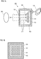
FIG. 1A and FIG. 1B are diagrams for describing a detection apparatus according to embodiment 1; -
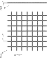
FIG. 2A and FIG. 2B are diagrams for describing an electromagnetic shielding according toembodiments 1 and 2; -
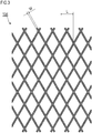
FIG. 3 is a diagram for describing another electromagnetic shielding according to embodiment 1; -
FIG. 4 is a diagram for describing another electromagnetic shielding according to embodiment 1; -
FIG. 5 is a diagram for describing another electromagnetic shielding according to embodiment 1; -
FIG. 6A is a diagram for describing a detection apparatus according toembodiment 2; -
FIG. 6B is a diagram for describing a detection apparatus according toembodiment 3; -
FIG. 7A and FIG. 7B are diagrams for describing an oscillation apparatus according toembodiment 2; -
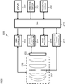
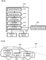
FIG. 8 is a diagram representing an example of a configuration of an imaging system according toembodiment 3; -
FIG. 9A is a diagram for describing an imaging system according to embodiment 4; and -
FIG. 9B is a diagram representing an example of a configuration of a moving object according to embodiment 4. - Hereinafter, embodiments of the present disclosure will be described with reference to the drawings. In the following description, a semiconductor apparatus which detects or oscillates terahertz waves and prevents unnecessary electromagnetic waves (millimeter waves) from leaking to the outside without obstructing detection or oscillation of terahertz waves by using an electromagnetic shielding in a mesh form will be described. In the following description, it is assumed that terahertz waves are electromagnetic waves (radio waves) having signals of any frequency band in a frequency range of 0.3 THz to 3 THz (at least 0.3 THz and not more than 3 THz). Furthermore, it is assumed below that millimeter waves are electromagnetic waves (radio waves) having signals of any frequency band in a frequency range of 30 GHz to 300 GHz (at least 30 GHz and less than 300 GHz).
- An overview of a terahertz-wave detection apparatus 100 (semiconductor apparatus; terahertz-wave camera) according to embodiment 1 will be described using
FIG. 1A to FIG. 2B .FIG. 1A is a diagram for describing a configuration of thedetection apparatus 100 and is a side view of thedetection apparatus 100.FIG. 1B is a front view of thedetection apparatus 100 ofFIG. 1A . - The
detection apparatus 100 includes anelement substrate 101, acircuit board 102, ahousing 103, anelectromagnetic shielding 104, and amonitor 106. In addition,terahertz waves 201 which are electromagnetic waves are radiated from atest object 300 to the front of thedetection apparatus 100. Here, theterahertz waves 201 are terahertz waves generated by thetest object 300 according to thermal radiation or terahertz waves radiated from external lighting and reflected by thetest object 300. Further, theterahertz waves 201 may be within a frequency range of 0.3 THz to 3 THz and thus 0.1 mm to 1 mm can be obtained as wavelengths. - A plurality of
elements 151 having spectral sensitivity for theterahertz waves 201 are arranged in a matrix form (two-dimensionally) on theelement substrate 101. Theelements 151 are, for example, semiconductor devices having a structure in which Schottky barrier diodes (SBDs) fabricated using a compound semiconductor or a semiconductor and antennas are integrated such that they have spectral sensitivity for the terahertz waves 201. Further, theelements 151 may be rectification type detection elements such as self-switching diodes and metal-insulator-metal (MIM) diodes, transistors such as field effect transistors (FETs) and high electron mobility transistors (HEMTs) or detection elements using quantum wells. In a terahertz-wave camera, theelements 151 correspond to pixels. - A circuit which reads signals output from the
elements 151 is formed on thecircuit board 102 and electrically connected to theelements 151 of the element substrate 101 (not shown). Here, signals output from theelements 151 are related to the terahertz waves 201. Thecircuit board 102 includes an amplification circuit, a filter circuit, a switch circuit, a power supply circuit, and the like. For example, a general-purpose semiconductor circuit technology such as a CMOS circuit technology can be applied to thecircuit board 102. The circuit formed on thecircuit board 102 can provide high-definition images by rapidly reading signals from theelements 151 and performing imaging processing thereon as a terahertz-wave camera. - In such a configuration, unnecessary
electromagnetic waves 211 are generated from theelement substrate 101 on which theelements 151 are arranged, thecircuit board 102 and the like due to rapid reading and rapid processing of signals from theelements 151. - In the present embodiment, the
circuit board 102 is formed and disposed integrally with theelement substrate 101, but the configuration is not limited thereto and thecircuit board 102 and theelement substrate 101 may be separately formed and separately disposed. - The
housing 103 accommodates theelement substrate 101 and thecircuit board 102. In addition, thehousing 103 stores theelement substrate 101 and thecircuit board 102 at predetermined positions and shields them such that the unnecessaryelectromagnetic waves 211 do not leak to the outside. - The
monitor 106 can display an imaged terahertz wave image. Here, thedetection apparatus 100 detects the terahertz waves 201 from thetest object 300 and images the terahertz waves 201 through theelement substrate 101 and thecircuit board 102. - The
electromagnetic shielding 104 is formed of a conductive material in a mesh form and disposed in front of asurface 105 of theelement substrate 101 which detects the terahertz waves 201. Theelectromagnetic shielding 104 prevents the aforementioned unnecessaryelectromagnetic waves 211 generated from theelement substrate 101 and thecircuit board 102 from leaking to the outside by being formed of the conductive material. Here, theelectromagnetic waves 211 are electromagnetic waves that are not more than microwave bands having frequencies not more than several GHz which are increasingly demanded in radio and transceivers as well as recent communications. That is, wavelengths of theelectromagnetic waves 211 are greater (longer) than those of the terahertz waves 201. - Here, while the mesh form of the
electromagnetic shielding 104 is not particularly limited, an example of a most typical configuration in which thin metal wires are woven in vertical and horizontal directions in a lattice shape at nearly equal intervals is shown inFIG. 2A and FIG. 2B for simplification of explanation.FIG. 2A is a front view of theelectromagnetic shielding 104 viewed in an advancing direction of the terahertz waves 201 andFIG. 2B is a side view of theelectromagnetic shielding 104. - Hereinafter, conditions for line widths, sizes (widths) of opening portions and a line thickness of the
electromagnetic shielding 104 for preventing leakage of theelectromagnetic waves 211 without obstructing detection of the terahertz waves 201 will be described. - First, line widths W1 and W2 of the
electromagnetic shielding 104 are set such that they are not more than the wavelength of the terahertz waves 201 used for detection, desirably not more than 1/2 of the wavelength, and more desirably not more than 1/5 of the wavelength. - According to this, the terahertz waves 201 radiated from the
test object 300 can arrive at theelements 151 while receiving little influence from the mesh-form electromagnetic shielding because obstacles that are smaller than the waveform have little influence on electromagnetic waves (radio waves). - In the present embodiment, sizes (widths) L1 and L2 of opening portions of the
electromagnetic shielding 104 are set such that they are at least the wavelength of the terahertz waves 201 detected by theelements 151 and not more than 1/2 of the wavelength of theelectromagnetic waves 211 to be shielded. Here, in order to shield theelectromagnetic waves 211 using the conductive material of the mesh, it is necessary to set the sizes L1 and L2 of the opening portions of the mesh to be no more than at least half the wavelength of theelectromagnetic waves 211 such that the wavelength of theelectromagnetic waves 211 is a shielding wavelength. Further, theelectromagnetic waves 211 to be shielded (to be prevented from leaking) are desirably millimeter waves. Here, millimeter waves are electromagnetic waves having signals of any frequency band in a frequency range of 30 GHz to 300 GHz (at least 30 GHz and not more than 300 GHz), as described above. Accordingly, millimeter waves can have values greater than 1.0 mm and not more than 10.0 mm as wavelengths. Meanwhile, in order to suppress theelectromagnetic waves 211 from leaking to the surroundings and obtain a sufficient shielding effect (shield effect), it is desirable that the sizes L1 and L2 of the opening portions of the mesh be smaller and it is more desirable that they not be more than 1/5 of the wavelength of theelectromagnetic waves 211, and even more desirable that they be 1/10 of the wavelength. - Furthermore, the sizes L1 and L2 of the opening portions of the
electromagnetic shielding 104 also need to be at least the wavelength of the terahertz waves 201 detected by theelements 151. This is for the purpose of causing the terahertz waves 201 radiated from thetest object 300 to arrive at theelements 151 while receiving little influence from theelectromagnetic shielding 104. If these conditions for the sizes of the opening portions of theelectromagnetic shielding 104 are satisfied, a high-definition terahertz-wave camera using the terahertz waves 201 can be provided. - In addition, since the sizes L1 and L2 of the opening portions are not more than 1/2 of the wavelength of the unnecessary
electromagnetic waves 211 generated from theelement substrate 101 and thecircuit board 102, it is possible to effectively shield theelectromagnetic waves 211 to suppress leakage to the outside and prevent electromagnetic interference (radio interference). - A line thickness t1 of the
electromagnetic shielding 104 shown inFIG. 2B is set such that it is not more than the wavelength of the terahertz waves 201 used for detection, desirably not more than 1/2 of the wavelength because the line affects theterahertz waves 201 when it is excessively thick. - That is, it is possible to effectively shield the unnecessary
electromagnetic waves 211 without obstructing detection of the terahertz waves 201 according to presence of theelectromagnetic shielding 104. In addition, when the wavelength of the terahertz waves 201 in the present embodiment is defined as λ and the wavelength of theelectromagnetic waves 211 to be shielded is defined as λ2, the line widths W1 and W2 or the line thickness t1 of theelectromagnetic shielding 104 satisfies (1) or (3) below. Accordingly, the effect that detection of the terahertz waves 201 is not obstructed can be additionally obtained. Furthermore, it is possible to shield the unnecessaryelectromagnetic waves 211 from leaking to the outside more effectively without obstructing detection of theterahertz waves 201 when the sizes (widths) L1 and L2 of the opening portions of theelectromagnetic shielding 104 satisfy (2) below. - (1) W1 ≤ λ and W2 ≤ λ
- (2) λ ≤ L1 ≤ λ2/2 and λ ≤ L2 ≤ λ2/2
- (3) t1 ≤ λ
- Other examples of the mesh form of the
electromagnetic shielding 104 will be described usingFIG. 3 to FIG. 5 . - The
electromagnetic shielding 104 ofFIG. 3 has metal wires which are arranged such that opening portions have a diamond shape. In such a mesh form, it is desirable that the length L (the size of opening portions; the length of a shorter diagonal line) of a shorter one of distances between opposite vertexes in the opening portions be set to no more than 1/2 of the wavelength of theelectromagnetic waves 211 required to be shielded. Here, it is desirable that the length L be at least the wavelength of the terahertz waves 201 such that detection of the terahertz waves 201 is not obstructed. Furthermore, it is desirable that a line width W and a line thickness t1 (not shown) also be set to at least no more than the wavelength of the terahertz waves 201 to be detected. - The
electromagnetic shielding 104 ofFIG. 4 has metal wires which are arranged such that opening portions have a hexagonal shape. In such a mesh form, it is also desirable that a distance L (the size of the opening portions) between two opposite sides in the opening portions be set to no more than 1/2 of the wavelength of theelectromagnetic waves 211 required to be shielded. Here, it is desirable that the length L be at least the wavelength of the terahertz waves 201 such that detection of the terahertz waves 201 is not obstructed. Furthermore, it is desirable that a line width W and a line thickness t1 (not shown) also be set to at least no more than the wavelength of the terahertz waves 201 to be detected. - Meanwhile, with respect to the
electromagnetic shielding 104 having different widths of opening portions depending on directions like the shapes shown inFIG. 3 andFIG. 4 , dimensions, installation directions and the like can be appropriately set in consideration of a polarization direction of theelectromagnetic waves 211 to be shielded and the like. - In the
electromagnetic shielding 104 ofFIG. 5 , circular opening portions with a diameter L are arranged honeycomb dot (zigzag) at an adjacent pitch P (adjacent interval) in directions of 0° and 60°. In addition, the diameter L of the opening portions (the size of the opening portions) is set to no more than 1/2 of the wavelength of theelectromagnetic waves 211 required to be shielded. Here, it is desirable that the diameter L be at least the wavelength of the terahertz waves 201 such that detection of the terahertz waves 201 is not obstructed. Meanwhile, when the aforementioned examples of various shapes of theelectromagnetic shielding 104 are taken into account, the size (width) of the opening portions can be regarded as twice a shortest distance between the center position of an opening portion and the metal wire forming the opening portion. Furthermore, the size (width) of the opening portions can also be regarded as a shortest length, which is included in the insides of a corresponding opening portion (first opening portion) and another opening portion (second opening portion), of a line segment connecting the center position of the corresponding opening portion (first opening portion) and a center position of another opening portion (second opening portion) adjacent to the corresponding opening portion. In addition, the size (width) of the opening portions can also be regarded as a shortest length, which is included in the insides of a corresponding opening portion (first opening portion) and another opening portion (second opening portion), of a straight line connecting the center position of the corresponding opening portion (first opening portion) and a center position of another opening portion (second opening portion) adjacent to the corresponding opening portion. - For the zigzag-shaped mesh shown in
FIG. 5 , a processing method such as punching processing, etching, laser processing or expanding a metal plate is generally used. The circular opening portions can uniformly shield theelectromagnetic waves 211 without depending on a polarization direction of theelectromagnetic waves 211 to be shielded and thus have the advantage of easy placement. Here, regarding the line widths W when the light-shielding portions are not on uniform lines as shown inFIG. 5 , an average line width is defined as W in consideration of the overall influence on the terahertz waves 201. Here, the width W is, for example, the average of an interval w1 between opening portions neighboring in the 0° direction and an interval w2 (the size L of the opening portions) between opening portions neighboring in the 90° direction. In addition, it is desirable that the line width W and the line thickness t1 of the electromagnetic shielding 104 (not shown) be set to at least no more than the wavelength of the terahertz waves 201 to be detected. - Meanwhile, the shape of the
electromagnetic shielding 104 are not limited to the shapes shown inFIG. 2A to FIG. 5 and other polygonal shapes, an oval shape, an elliptical shape, additionally deformed shapes, and the like can be appropriately selected in consideration of the wavelength and polarization direction of theelectromagnetic waves 211 to be shielded, ease of processing of members, and the like. Furthermore, a manufacturing method of theelectromagnetic shielding 104 is not limited to metal wire weaving and can be arbitrarily determined as weaving or bonding of a fiber containing a conductive material, etching, laser processing or expanding a conductive plate, or the like in view of easiness of handling considering necessary dimensions and costs. Moreover, a manufacturing method of patterning a conductive film on a quartz substrate or a polyethylene substrate having a high permeability for the terahertz waves 201 can also be selected. - A terahertz wave reception apparatus is used in embodiment 1, whereas a terahertz wave oscillation apparatus (semiconductor apparatus) is used in
embodiment 2.FIG. 7A and FIG. 7B are schematic configuration diagrams of an oscillation apparatus (terahertz light source) in the present embodiment. -
FIG. 7A is a diagram for describing a configuration of anoscillation apparatus 110 and is a side view of theoscillation apparatus 110.FIG. 7B is a diagram for describing a component near anelement substrate 111 which oscillates terahertz waves and is a front view with respect to oscillatingterahertz waves 202 ofFIG. 7A . - The
oscillation apparatus 110 includes theelement substrate 111 on which a plurality ofelements 161 which oscillate the terahertz waves 202 are formed in a matrix form (two-dimensionally), and acircuit board 112 which controls theelements 161. These components are accommodated in ahousing 113, and thehousing 113 has functions of storing these components at predetermined positions and shielding unnecessaryelectromagnetic waves 211 from leakage to the outside. - In addition, the
electromagnetic shielding 104 is disposed in front of thesurface 115 of theelement substrate 111 which oscillates the terahertz waves 202. - An oscillation element including an active element (negative resistance element) such as a resonance tunnel diode, an Esaki diode or a Gunn diode and a resonance structure (antenna) can be used as the
elements 161. The configuration of theelements 161 is not limited thereto and known terahertz-wave oscillating devices (semiconductor devices) may be used. - A driving circuit for oscillating the
terahertz waves 202 from theelements 161 and controlling them is formed on thecircuit board 112. Thecircuit board 112 is electrically connected to therespective elements 161 of theelement substrate 111. That is, the driving circuit in thecircuit board 112 oscillates the terahertz waves 202 from theelements 161 by driving therespective elements 161 of theelement substrate 111. Thecircuit board 112 includes a filter circuit, a switch circuit, a power supply circuit and the like, and a general-purpose semiconductor circuit technology, for example, a CMOS circuit technology, can be applied thereto. - In the
oscillation apparatus 110 having this configuration, the unnecessaryelectromagnetic waves 211 are generated from theelement substrate 111 on which theelements 161 are arranged, thecircuit board 112 and the like due to rapid driving or rapid processing of theelements 161 as in thedetection apparatus 100 described in embodiment 1. - The
electromagnetic shielding 104 is disposed in front of thesurface 115 of theelement substrate 111 which oscillates the terahertz waves 202, and transmits the necessary terahertz waves 202 and while shielding the unnecessaryelectromagnetic waves 211 as in embodiment 1. - Meanwhile, the configuration of the
electromagnetic shielding 104 is the same as that ofFIG. 2A and FIG. 2B shown in embodiment 1. In addition, conditions for line widths W1 and W2, conditions for sizes L1 and L2 of opening portions and conditions for a line thickness t1 in theelectromagnetic shielding 104 are the same as those when "terahertz waves 201" is replaced with "terahertz waves 202" in embodiment 1. - Accordingly, it is possible to shield the unnecessary
electromagnetic waves 211 without obstructing oscillation of the terahertz waves 202 in the present embodiment. - The
detection apparatus 100 according to example 1 that is a specific example of embodiment 1 will be described with reference toFIG. 1A to FIG. 2B . - Here, the
detection apparatus 100 is a radio-wave camera, and radio-wave cameras include a passive type that selects and detects desired radio waves from among electromagnetic waves (radio waves and light) generated from a test object according to thermal radiation, and an active type that detects reflected radio waves obtained by radiating desired radio waves to a test object. Many passive type radio-wave cameras realize selection of radio waves and low nose of a system using a high-frequency circuit such as a mixer because radio waves generated from a test object according to thermal radiation are very weak. Since high-frequency circuit technology operating in the terahertz band is under development, there are many ongoing studies on an active type terahertz-wave camera in order to secure a necessary SN ratio. Meanwhile, a terahertz-wave camera of the present example is an active type terahertz-wave camera which radiates terahertz waves to a test object. - In the present example, the terahertz waves 201 are reflected waves that have been radiated to the
test object 300 from a terahertz-wave lighting which is not shown and reflected by thetest object 300. The terahertz-wave lighting uses a surface light source in which a plurality of terahertz-wave light sources are arranged in a matrix form. More specifically, a terahertz wave source is an element in which a resonance tunnel diode (RTD) and a patch antenna that is a resonator are integrated, and the output of the terahertz wave source is slightly less than 0.1 mW. In this example, terahertz-wave lighting is a surface light source in which terahertz wave sources are arranged as 25 elements. Meanwhile, the number of arranged terahertz-wave sources is not limited thereto. Further, the configuration of the terahertz-wave sources is not also limited thereto and known terahertz-wave light sources can be used. - As the
elements 151 which detect the terahertz waves 201, Schottky barrier diodes (SBDs) in which antennas are integrated are used. Antennas are loop antennas and a resonant frequency of the antennas is adjusted to a frequency of the terahertz waves 201 generated from RTDs, 0.5 THz. In addition, theelements 151 are photoelectric conversion elements which convert signals of the terahertz waves 201 into electrical signals. - A total of 22,500
elements 151 are arranged in 150 rows × 150 columns in a matrix form (two-dimensionally) on the surface of theelement substrate 101. Theelement substrate 101 has a size of 55 mm × 55 mm. - The
circuit board 102 includes a line reading circuit formed thereon and is composed of a switch circuit and a shift register circuit for selecting a line, a bias circuit for determining operating points of theelements 151 of theelement substrate 101, a circuit for converting outputs of theelements 151 into charge signals, and the like. These circuits are formed on a silicon-based semiconductor substrate. - Output of the
circuit board 102 is connected to an amplification circuit, a filter circuit, a correlated double sampling (CDS) circuit and the like which are not shown such that signals related to the terahertz waves 201 are adjusted. These circuits may be included in thecircuit board 102. Thedetection apparatus 100 acquires a strength distribution of signals related to the terahertz waves 201 by sequentially selecting rows of the element substrate 101 (sensor part) and acquiring signals ofelements 151 included in the rows. In addition, thedetection apparatus 100 constructs strength distribution images of the terahertz waves 201 (which are also called terahertz wave images) by arranging the signals of the strength distribution with reference to row selection positions of theelement substrate 101. In construction, thedetection apparatus 100 may perform image processing such as averaging of terahertz wave images, removal of unnecessary fixed patterns, and γ correction. - In addition, the
monitor 106 presents terahertz wave images to a user in the present example. - The
electromagnetic shielding 104 is an electromagnetic shielding in a metal mesh shape in which thin metal wires are woven in vertical and horizontal directions at approximately equal intervals, shown inFIG. 2A . - In addition, line widths W1 and W2 and a line thickness t of the
electromagnetic shielding 104 are set to 0.12 mm (λ/5) and sizes L1 and L2 of opening portions are set to 6 mm for the frequency 0.5 THz (wavelength λ = 0.6 mm) of the terahertz waves 201 detected by theelements 151. According to this configuration, it is possible to shield electromagnetic noise of not more than the microwave band used for communication and the like without attenuating the terahertz waves 201 to be detected, which will be described in detail later. - Meanwhile, the line widths W1 and W2 and the sizes L1 and L2 of the opening portions of the
electromagnetic shielding 104 are not limited thereto and can be appropriately set depending on frequencies of the terahertz waves 201 to be used, theelectromagnetic waves 211 to be shielded and the shielding effect. Furthermore, the configuration of theelectromagnetic shielding 104 and the form of the mesh are not limited to the lattice shape shown inFIG. 2A , and a mesh shape, material and manufacturing method can be appropriately selected in consideration of the shielding effect and easiness of handling members. - Here, operations of the terahertz waves 201 and unnecessary
electromagnetic waves 211 in the present example will be described. The terahertz waves 201 radiated from a terahertz-wave lighting to thetest object 300 and reflected from thetest object 300 passes through theelectromagnetic shielding 104 and then reaches theelement substrate 101. While the terahertz waves 201 have a wavelength λ of 0.6 mm, the line widths W1 and W2 and thickness t of theelectromagnetic shielding 104 are 0.12 mm which is sufficiently thin and the thickness is also sufficiently thin. Accordingly, the terahertz waves 201 hardly attenuate when passing. This is because scattering or reflection occurs when a material present on a path of incident electromagnetic waves is larger than the wavelength of the electromagnetic waves but scattering or reflection hardly occurs and attenuation is insignificant when the material is smaller or thinner than the wavelength. The terahertz waves 201 arrived at theelement substrate 101 are subjected to image processing, as described above, and reflected (displayed) on themonitor 106 as terahertz wave images. Here, the terahertz waves 201 arrived at theelement substrate 101 hardly attenuate and thus are displayed as fine images. - Simultaneously, high-frequency current flows through electronic elements and wires in the
circuit board 102 and an image processing circuit or a high voltage is applied thereto, and thus the high-frequencyelectromagnetic waves 211 are generated. It is known that the generatedelectromagnetic waves 211 have a large amount of frequency components of several MHz to several GHz and components of 10 GHz or higher are hardly generated. Theelectromagnetic waves 211 propagates in various directions from a place where they have been generated. Although some of theelectromagnetic waves 211 are input to the rear surface and side of thehousing 103, theelectromagnetic waves 211 are reflected or absorbed without leaking to the outside after input to thehousing 103 because thehousing 103 is formed of a conductive material. - In addition, the
electromagnetic waves 211 are input to theelectromagnetic shielding 104 like the terahertz waves 201. While theelectromagnetic waves 211 of several MHz to several GHz have a wavelength of at least 30 mm, the sizes L1 and L2 of the opening portions are 6 mm less than λ/2 which is sufficiently narrow. Accordingly, theelectromagnetic waves 211 cannot transmit theelectromagnetic shielding 104 and are reflected or absorbed by theelectromagnetic shielding 104. Generally, it is known that electromagnetic waves have difficulty passing through opening portions present on the path of the electromagnetic waves and narrower than λ/2. This is because a lowest resonant frequency in the opening portions is the frequency of λ/2 that is the opening width and electromagnetic waves having frequencies lower than the frequency attenuate. That is, theelectromagnetic waves 211 do not go outside of the camera, and thus do not cause a problem of so-called electromagnetic interference (EMI) in which electromagnetic waves have a negative impact on electronic devices in the vicinity. - Even if some of frequencies higher than several MHz to several GHz in the
electromagnetic waves 211 go outside of the camera, nearby electronic devices do not malfunction at electromagnetic waves of the corresponding frequencies and the frequencies are not used for communication, and thus problems do not occur. In this manner, thedetection apparatus 100 transmits electromagnetic waves (terahertz waves 201) necessary for detection and imaging and prevents leakage of the unnecessaryelectromagnetic waves 211 and thus it operates as a terahertz-wave camera which obtains high-definition clear images. Although the unnecessaryelectromagnetic waves 211 can be prevented from leaking, for example, by thehousing 103 that is a metal plate on the side and rear surface of the camera, in general, imaging cannot be performed if a subject direction is shielded by the metal plate. With respect to this, it is possible to prevent leakage of the unnecessaryelectromagnetic waves 211 without deteriorating characteristics of the camera in the present example. - Furthermore, the frequency of the
electromagnetic waves 211 to be shielded can be determined depending on social communication devices or environments. In general, the frequency of theelectromagnetic waves 211 for which suppression of leakage is considered is assumed to be up to 6 GHz according to CISPR22 standard determined by International Special Committee on Radio Interference (CISPR) in many cases. This is because currently used communication devices are considered to be influenced by electromagnetic environments of up to 6 GHz and thus the influence is required to be suppressed socially. Accordingly, at the present time, when theelectromagnetic waves 211 at frequencies of not more than 6 GHz are shielded, the influence on other devices can be suppressed. - Meanwhile, although an example of a case in which the frequency of the terahertz waves 201 is 0.5 THz (wavelength λ = 0.6 mm) is represented in the present example, a low frequency among frequencies that the terahertz waves 201 can take is 300 GHz (wavelength λ = 1 mm). Accordingly, the widths W1 and W2 of the
electromagnetic shielding 104 may be not more than 1 mm. The thickness t1 of theelectromagnetic shielding 104 may also be not more than 1 mm for the same reason as that for the widths. - As described above, the unnecessary
electromagnetic waves 211 which become a problem due to leakage are regarded as not more than 6 GHz in the present social environment. To attenuate the unnecessaryelectromagnetic waves 211 that are not more than 6 GHz (wavelength 50.0 mm), it is desirable that the sizes L1 and L2 of the opening portions of theelectromagnetic shielding 104 be set to no more than 25.0 mm (not more than 25 mm). Further, it is also expected that frequencies of electromagnetic waves which become a problem due to leakage exceed 6 GHz due to recent development of high-frequency devices. Electromagnetic waves of up to 100 GHz are considered even in recommendation "ITU-RP. 372-8" of the International Telecommunication Union (ITU). In addition, electromagnetic waves at frequencies of at least 100 GHz greatly attenuate in the air and thus do not become a problem. Considering this, it is desirable that the sizes L1 and L2 of the opening portions of theelectromagnetic shielding 104 be set to no more than 1.5 mm in order to attenuate the unnecessaryelectromagnetic waves 211 that are not more than 100 GHz (wavelength 3 mm). According to this, it is possible to suppress the influence of unnecessary interfering electromagnetic waves with respect to all frequencies for which a leakage problem is conceived and provide a camera (semiconductor apparatus) which does not have a negative impact on other communication devices. - The detection apparatus 100 (terahertz-wave camera) of example 2 that is a specific example of embodiment 1 will be described using
FIG. 6A that is a schematic configuration diagram. Description of the same parts as those of example 1 is omitted. - As shown in
FIG. 6A , alens 107 is disposed between theelement substrate 101 and theelectromagnetic shielding 104. Theelement substrate 101 includes theelements 151 which detect the terahertz waves 201. That is, thelens 107 is disposed in front of thesurface 105 of theelement substrate 101 which detects the terahertz waves 201. - The terahertz waves 201 radiated from the
test object 300 are focused by thelens 107 and imaged on the plurality ofelements 151 formed on theelement substrate 101. That is, the optical path of the terahertz waves 201 is controlled by thelens 107. Accordingly, thedetection apparatus 100 can obtain clearer terahertz wave images than those in example 1. - A material that transmits the terahertz waves 201 can be applied as a material of the
lens 107. More specifically, a high-density polyethylene (HDPE), a Teflon (TM (registered trademark); PolyTetraFluoroethylene (PTFE)), a high-resistance silicon or the like can be applied as a material of thelens 107. - In addition, the frequency of the terahertz waves 201 to be detected by the
elements 151 is set to 2.0 THz (wavelength λ = 0.15 mm) in the present example. Furthermore, the line widths W1 and W2 and thickness t of theelectromagnetic shielding 104 are set to 0.05 mm (λ/3) and the sizes L1 and L2 of the opening portions are set to 0.15 mm. That is, the sizes L1 and L2 of the opening portions of theelectromagnetic shielding 104 are not more than 1.5 mm which can attenuate the unnecessaryelectromagnetic waves 211 that are not more than 100 GHz (wavelength 3 mm), and thus electromagnetic waves expected to be used for future communication can also be sufficiently shielded. - The detection apparatus 100 (terahertz-wave camera) of example 3 that is a specific example of embodiment 1 will be described using
FIG. 6B that is a schematic configuration diagram. Description of the same parts as those of example 2 is omitted. - Although the
lens 107 is disposed between theelectromagnetic shielding 104 and theelement substrate 101 in example 2, theelectromagnetic shielding 104 is disposed between theelement substrate 101 and thelens 107 in example 3. According to this configuration, it is possible to realize a more compact (smaller)detection apparatus 100 than that of example 2. - Example 4 that is a specific example of
embodiment 2 will be described with reference toFIG. 7A and FIG. 7B . Description of parts described inembodiment 2 is omitted. - The
elements 161 are elements (semiconductor devices) in which resonance tunnel diodes (RTDs) and patch antennas that are resonators are integrated and outputs of theelements 161 are a little less than 0.1 mW. In example 4, 100elements 161 having an oscillation frequency set to 0.375 THz (wavelength λ = 0.8 mm) are arranged in 10 rows × 10 columns in a matrix form. Meanwhile, the number of arrangedelements 161 is not limited thereto. Further, the configuration of theelements 161 is not also limited thereto and known terahertz-wave oscillation devices can be used. - A driving circuit for oscillating and controlling
terahertz waves 202 from theelements 161 is formed on thecircuit board 112. Thecircuit board 112 is electrically connected to therespective elements 161 of theelement substrate 111. Thecircuit board 112 includes a filter circuit, a switch circuit, a power supply circuit and the like, and a general-purpose semiconductor circuit technology, for example, a CMOS circuit technology can be applied thereto. - In the
oscillation apparatus 110 having this configuration, unnecessaryelectromagnetic waves 211 are generated from theelement substrate 111 on which theelements 161 are arranged, thecircuit board 112 and the like due to rapid driving or rapid processing of theelements 161 as in thedetection apparatus 100 described in examples 1 to 3. - The
electromagnetic shielding 104 is disposed in front of thesurface 115 of theelement substrate 111 which oscillates the terahertz waves 202. Theelectromagnetic shielding 104 transmits the necessary terahertz waves 202 and shields the unnecessaryelectromagnetic waves 211 as in examples 1 to 3. In addition, theelectromagnetic shielding 104 is configured such that the line widths W1 and W2 are not more than the wavelength λ of the terahertz waves 202 to be oscillated, desirably not more than 1/2 of the wavelength λ, more desirably not more than 1/5 of the wavelength λ as in examples 1 to 3. - In addition, the sizes L1 and L2 of the opening portions of the
electromagnetic shielding 104 are at least the wavelength λ of the terahertz waves 202 to be oscillated by theelements 161, not more than 1/2 of the wavelength of theelectromagnetic waves 211 to be shielded, desirably not more than 1/5, and more desirably not more than 1/10. - Specifically, the line widths W1 and W2 and thickness t1 are set to 0.2 mm and the sizes L1 and L2 of the opening portions are set to 0.9 mm in example 4.
- Meanwhile, the
lens 107 can be disposed in theoscillation apparatus 110 as in examples 2 and 3. That is, thelens 107 may be disposed in front of thesurface 115 of theelement substrate 111 which oscillates the terahertz waves 202. - According to this configuration, it is possible to effectively shield the unnecessary
electromagnetic waves 211 without attenuating the oscillating terahertz waves 202. - Although detected or oscillated electromagnetic waves are terahertz waves in the above-described
embodiments 1 and 2 and examples 1 to 4, detected or oscillated electromagnetic waves may be electromagnetic waves having any wavelength, for example, electromagnetic waves having a shorter wavelength than the terahertz waves. Likewise, the wavelength of electromagnetic waves shielded from leakage may also be electromagnetic wave having any wavelength. - An imaging system according to
embodiment 3 of the present disclosure will be described usingFIG. 8. FIG. 8 is a block diagram showing a schematic configuration of the imaging system according to the present embodiment. - The detection apparatus 100 (imaging apparatus) described in embodiment 1 is applicable to various imaging systems. Although imaging systems to which the
detection apparatus 100 is applicable are not particularly limited, for example, various apparatuses such as digital still cameras, digital camcorders, monitoring cameras, copying machines, facsimile, cellular phones, on-board cameras, observation satellites, and medical cameras are conceivable. In addition, a camera module including an optical system such as a lens and an imaging apparatus (photoelectric conversion apparatus) is also included in imaging systems.FIG. 8 illustrates a block diagram of a digital still camera as an example of such apparatuses. - As shown in
FIG. 8 , animaging system 2000 includes animaging apparatus 1000, an imagingoptical system 2002, aCPU 2010, alens controller 2012, animaging apparatus controller 2014, and animage processor 2016. In addition, theimaging system 2000 includes an irisdiaphragm shutter controller 2018, adisplay 2020, anoperation switch 2022, and arecording medium 2024. - The imaging
optical system 2002 is an optical system for forming an optical image of a subject and includes a lens group, aniris diaphragm 2004, and the like. Theiris diaphragm 2004 has a function as a shutter for controlling an exposure time during photographing of still images in addition to a function of controlling the amount of light during photographing by controlling the aperture thereof. The lens group and theiris diaphragm 2004 are held in an optical-axis direction such that they can advance and retreat and a magnification function (zooming function) and a focus control function are realized by operations of these components in connection. The imagingoptical system 2002 may be integrated into the imaging system or may be an imaging lens that can be attached to the imaging system. - The
imaging apparatus 1000 is disposed such that an imaging surface thereof is positioned in an image space of the imagingoptical system 2002. Theimaging apparatus 1000 is thedetection apparatus 100 described in embodiment 1 and includes a CMOS sensor (pixel part) and a peripheral circuit (peripheral circuit area) thereof. Theimaging apparatus 1000 constitutes a two-dimensional single-plate color sensor according to two-dimensional arrangement of pixels including a plurality of photoelectric converters and arrangement of color filters with respect to the pixels. Theimaging apparatus 1000 photoelectrically converts a subject image imaged by the imagingoptical system 2002 and outputs the converted image as an image signal and a focus detection signal. - The
lens controller 2012 is a component for performing a magnification operation and a focus control by controlling forward and backward driving of the lens group of the imagingoptical system 2002 and is composed of a circuit and a processing device configured to realize that function. The irisdiaphragm shutter controller 2018 is a component for changing the aperture of the iris diaphragm 2004 (varies a diaphragm value) to control the amount of light for photographing and is composed of a circuit and a processing device configured to realize that function. - The
CPU 2010 is a control device in the camera which executes various controls of the camera body and includes an arithmetic operation part, a ROM, a RAM, an A/D converter, a D/A converter, a communication interface circuit, and the like. TheCPU 2010 controls operations of respective parts of the camera according to a computer program stored in the ROM and the like and performs a series of photographing operations such as AF including detection of a focus state of the imaging optical system 2002 (focus detection), imaging, image processing and recording. TheCPU 2010 is also a signal processor. - The
imaging apparatus controller 2014 is a component for controlling operation of theimaging apparatus 1000, performing A/D conversion on a signal output from theimaging apparatus 1000 and transmitting the converted signal to theCPU 2010 and is composed of a circuit and a processing device configured to realize those functions. The A/D conversion function may be included in theimaging apparatus 1000. Theimage processor 2016 is a processing device which generates an image signal by performing image processing such as γ conversion and color interpolation on an A/D converted signal and is composed of a circuit and a processing device configured to realize that function. Thedisplay 2020 is a display device such as a liquid crystal display (LCD) and displays information about a photographing mode of the camera, a preview image before photographing, an image for checking after photographing, a focusing state during focus detection, and the like. Theoperation switch 2022 is composed of a power switch, a release (photographing trigger) switch, a zoom operation switch, a photographing mode selection switch, and the like. Therecording medium 2024 is a component for recording photographed images and the like and may be embedded in the imaging system or may be a detachable component such as a memory card. - In this manner, an imaging system with high performance can be realized by configuring the
imaging system 2000 to which thedetection apparatus 100 according to embodiment 1 is applied. - An imaging system and a mobile body according to embodiment 4 of the present disclosure will be described using
FIG. 9A and FIG. 9B. FIG. 9A and FIG. 9B are diagrams showing configurations of an imaging system and a moving object according to the present embodiment. -
FIG. 9A shows an example of animaging system 2100 with respect to an on-board camera. Theimaging system 2100 includes animaging apparatus 2110. Theimaging apparatus 2110 is thedetection apparatus 100 described in the above-described embodiment 1. Theimaging system 2100 includes animage processor 2112 which is a processing device for performing image processing on a plurality of pieces of image data acquired by theimaging apparatus 2110. Theimaging system 2100 includes aparallax acquisition unit 2114 which is a processing device for calculating a parallax (a phase difference of parallax images) from a plurality of pieces of image data acquired by theimaging apparatus 2110. In addition, theimaging system 2100 includes adistance acquisition unit 2116 which is a processing device for calculating a distance to an object on the basis of a calculated parallax. Theimaging system 2100 includes acollision determination unit 2118 which is a processing device for determining whether there is a possibility of collision on the basis of a calculated distance. Here, theparallax acquisition unit 2114 and thedistance acquisition unit 2116 are an example of an information acquisition means for acquiring information such as information on a distance to an object. That is, distance information is information about a parallax, a defocus amount, a distance to an object, and the like. Thecollision determination unit 2118 may determine a possibility of collision using any of such distance information. The aforementioned processing devices may be realized by hardware designed for dedicated purposes or realized by general-purpose hardware which performs arithmetic operations on the basis of a software module. Furthermore, the processing devices may be realized by field programmable gate arrays (FPGAs), application specific integrated circuits (ASICs) or the like. Moreover, the processing devices may be realized by a combination thereof. - The
imaging system 2100 is connected to a vehicleinformation acquisition device 2120 and can acquire vehicle information such as a vehicle speed, a yaw rate and a steering angle. In addition, theimaging system 2100 is connected to acontrol ECU 2125 which is a control device for outputting a control signal for generating braking power for a vehicle on the basis of a determination result of thecollision determination unit 2118. That is, thecontrol ECU 2125 is an example of a moving object control means for controlling a moving object on the basis of distance information. Furthermore, theimaging system 2100 is also connected to awarning device 2140 for giving a warning to a driver on the basis of a determination result of thecollision determination unit 2118. For example, in case of a high possibility of collision as a determination result of thecollision determination unit 2118, thecontrol ECU 2125 may perform vehicle control for avoiding a collision and reducing damage by braking the vehicle, returning the accelerator, and suppressing engine power. Thewarning device 2140 warns a user by performing operations of giving an alarm such as sound, displaying warning information on a screen of a car navigation system or the like, vibrating a seatbelt or steering, and the like. - In the present embodiment, the surrounding of a vehicle, for example, the front or back is imaged using the
imaging system 2100.FIG. 9B shows theimaging system 2100 when the front of a vehicle (imaging range 2150) is imaged. The vehicleinformation acquisition device 2120 transmits an instruction for operating theimaging system 2100 to perform imaging. Theimaging system 2100 of the present embodiment can improve distance measurement accuracy by using thedetection apparatus 100 of the above-described embodiment 1 as theimaging apparatus 2110. - Although an example of controlling a vehicle such that the vehicle does not collide with other vehicles has been described above, the present disclosure is also applicable to control of automated driving while following other vehicles, control of automated driving within lanes, and the like. Furthermore, the imaging system is not limited to vehicles such as cars and can be applied to, for example, moving objects (transportation apparatuses) such as ships, aircrafts or industrial robots. Moving devices in moving objects (transportation apparatuses) are various driving sources such as an engine, a motor, a vehicle wheel and a propeller. In addition, the present disclosure is not limited to moving objects and can be applied to apparatuses using wide object recognition, such as an intelligent transport system (ITS).
- Configurations and processing described in the above-described embodiments and examples of the present disclosure can be arbitrarily combined and used.
- While the present invention has been described with reference to exemplary embodiments, it is to be understood that the invention is not limited to the disclosed exemplary embodiments. The scope of the following claims is to be accorded the broadest interpretation so as to encompass all such modifications and equivalent structures and functions.
- A semiconductor apparatus (100) comprising: an element substrate (101) including a plurality of semiconductor devices (151) adapted to detect or oscillate predetermined electromagnetic waves; and an electromagnetic shielding (104) in a mesh form disposed in front of a surface detecting or oscillating the predetermined electromagnetic waves in the element substrate (101) and formed of a conductive material, wherein a line width of the electromagnetic shielding (104) is not more than 1 mm or not more than a wavelength of the predetermined electromagnetic waves.
Claims (12)
- A semiconductor apparatus (100) comprising:an element substrate (101) including a plurality of semiconductor devices (151) adapted to detect or oscillate predetermined electromagnetic waves; andan electromagnetic shielding (104) in a mesh form disposed in front of a surface detecting or oscillating the predetermined electromagnetic waves in the element substrate (101) and formed of a conductive material, whereina line width of the electromagnetic shielding (104) is not more than 1 mm or not more than a wavelength of the predetermined electromagnetic waves.
- The semiconductor apparatus (100) according to claim 1, wherein
predetermined electromagnetic waves are terahertz waves; and
the line width of the electromagnetic shielding (104) is not more than a wavelength of the terahertz waves. - The semiconductor apparatus (100) according to claim 2, wherein the width of each opening portion of the electromagnetic shielding (104) is at least the wavelength of the terahertz waves and not more than 1/2 of a wavelength of millimeter waves.
- The semiconductor apparatus (100) according to claim 2 or 3, wherein the thickness of the electromagnetic shielding (104) is not more than the wavelength of the terahertz waves.
- The semiconductor apparatus (100) according to any one of claims 1 to 4, further comprising a circuit board (102) including a circuit adapted to read signals output from the plurality of semiconductor devices (151) or drive the plurality of semiconductor devices (151), wherein
the plurality of semiconductor devices (151) are two-dimensionally arranged on the element substrate (101), and the circuit board (102) and the element substrate (101) are integrally disposed. - The semiconductor apparatus (100) according to any one of claims 1 to 5, further comprising a lens (107) adapted to control an optical path of the predetermined electromagnetic waves, wherein
the lens (107) is disposed in front of the surface detecting or oscillating the predetermined electromagnetic waves in the element substrate (101). - The semiconductor apparatus (100) according to any one of claims 1 to 6, wherein the wavelength of the predetermined electromagnetic waves is in a range of 0.1 mm to 1 mm.
- The semiconductor apparatus (100) according to any one of claims 1 to 7, wherein the width of each opening portion of the electromagnetic shielding (104) is not more than 25 mm.
- The semiconductor apparatus (100) according to claim 8, wherein the width of each opening portion of the electromagnetic shielding (104) is not more than 1.5 mm.
- The semiconductor apparatus (100) according to any one of claims 1 to 9, wherein the thickness of the electromagnetic shielding (104) is not more than 1 mm.
- An imaging system (2000) comprising:the semiconductor apparatus (100) according to any one of claims 1 to 10; anda signal processor (2016) configured to process signals output from the semiconductor apparatus.
- A moving object comprising:the semiconductor apparatus (100) according to any one of claims 1 to 10;a moving device;a processing device (2112, 2114, 2116, 2118) configured to acquire information from signals output from the semiconductor apparatus; anda control device (2125) configured to control the moving device on the basis of the information.
Applications Claiming Priority (1)
| Application Number | Priority Date | Filing Date | Title |
|---|---|---|---|
| JP2019011827A JP7208032B2 (en) | 2019-01-28 | 2019-01-28 | semiconductor equipment |
Publications (2)
| Publication Number | Publication Date |
|---|---|
| EP3686937A1 true EP3686937A1 (en) | 2020-07-29 |
| EP3686937B1 EP3686937B1 (en) | 2023-04-05 |
Family
ID=69326380
Family Applications (1)
| Application Number | Title | Priority Date | Filing Date |
|---|---|---|---|
| EP20153800.6A Active EP3686937B1 (en) | 2019-01-28 | 2020-01-27 | Semiconductor apparatus for detecting or oscillating electromagnetic waves, imaging system, and moving object |
Country Status (4)
| Country | Link |
|---|---|
| US (1) | US11309257B2 (en) |
| EP (1) | EP3686937B1 (en) |
| JP (1) | JP7208032B2 (en) |
| CN (1) | CN111487645A (en) |
Cited By (1)
| Publication number | Priority date | Publication date | Assignee | Title |
|---|---|---|---|---|
| EP4186798A1 (en) * | 2021-11-30 | 2023-05-31 | Airbus SAS | Shielding arrangement for aircraft wiring |
Families Citing this family (7)
| Publication number | Priority date | Publication date | Assignee | Title |
|---|---|---|---|---|
| GB2593530A (en) * | 2020-03-27 | 2021-09-29 | Bae Systems Plc | Impact shield structures |
| CN116762287A (en) * | 2020-12-31 | 2023-09-15 | 华为技术有限公司 | A receiver, chip and electronic device |
| JP7851175B2 (en) * | 2022-04-15 | 2026-04-24 | キヤノン株式会社 | Antenna device, communication device, and imaging system |
| CN115128362B (en) * | 2022-06-10 | 2024-07-30 | 电子科技大学 | In-situ test device and test method for electromagnetic shielding effectiveness of optical window |
| CN118510146B (en) * | 2023-02-16 | 2025-11-21 | 鹏鼎控股(深圳)股份有限公司 | Circuit board for transmitting terahertz frequency signals and manufacturing method thereof |
| CN117406213B (en) * | 2023-11-16 | 2025-03-11 | 深圳市安卫普科技有限公司 | A detection device |
| JP7798242B1 (en) * | 2025-05-07 | 2026-01-14 | 三菱電機株式会社 | Terahertz imaging device and terahertz imaging method |
Citations (6)
| Publication number | Priority date | Publication date | Assignee | Title |
|---|---|---|---|---|
| US5481400A (en) * | 1993-11-09 | 1996-01-02 | Hughes Aircraft Company | Survivable window grids |
| US20050212100A1 (en) * | 2004-03-26 | 2005-09-29 | Sharp Kabushiki Kaisha | Semiconductor device for optical communication and manufacturing method therefor |
| JP2008010811A (en) | 2006-05-31 | 2008-01-17 | Canon Inc | Electromagnetic wave oscillator |
| US20120241615A1 (en) * | 2011-03-23 | 2012-09-27 | Seiko Epson Corporation | Terahertz wave detection device, terahertz wavelength filter, imaging device, and measurement device |
| CN104993199A (en) * | 2015-08-07 | 2015-10-21 | 电子科技大学 | Ultrathin terahertz medium high frequency broad band filter and manufacturing method for the same |
| EP3293772A1 (en) * | 2016-09-08 | 2018-03-14 | Goodrich Corporation | Apparatus and methods of electrically conductive optical semiconductor coating |
Family Cites Families (19)
| Publication number | Priority date | Publication date | Assignee | Title |
|---|---|---|---|---|
| JP4303603B2 (en) * | 2004-01-13 | 2009-07-29 | 株式会社日立製作所 | Nuclear medicine diagnostic device and its detector unit |
| JP4634836B2 (en) * | 2004-03-26 | 2011-02-16 | 三菱電機株式会社 | High frequency package, transceiver module and radio apparatus |
| WO2007138813A1 (en) | 2006-05-31 | 2007-12-06 | Murata Manufacturing Co., Ltd. | Metal plate for wire grid, wire grid, and method of producing metal plate for wire grid |
| JP2008160454A (en) | 2006-12-22 | 2008-07-10 | Sumitomo Electric Ind Ltd | Far-infrared imaging device |
| JP5392888B2 (en) * | 2008-07-08 | 2014-01-22 | 独立行政法人理化学研究所 | Near-field terahertz photodetector |
| WO2011142155A1 (en) | 2010-05-12 | 2011-11-17 | 株式会社村田製作所 | Method for measuring characteristics of object to be measured, and gap arrangement structure and measuring device used therefor |
| JP5735824B2 (en) * | 2011-03-04 | 2015-06-17 | キヤノン株式会社 | Information acquisition apparatus and information acquisition method |
| WO2012132111A1 (en) * | 2011-03-31 | 2012-10-04 | 株式会社村田製作所 | Measurement structure, method for producing same, and measurement method using same |
| JP2013104804A (en) * | 2011-11-15 | 2013-05-30 | Seiko Epson Corp | Semiconductor short pulse generating device, terahertz-wave generating device, camera, imaging device, and measuring device |
| WO2013073242A1 (en) * | 2011-11-18 | 2013-05-23 | 株式会社村田製作所 | Periodic structure and measurement method employing same |
| JP5910064B2 (en) * | 2011-12-20 | 2016-04-27 | セイコーエプソン株式会社 | Photoconductive antenna, terahertz wave generator, camera, imaging device, and measuring device |
| JP6168726B2 (en) | 2012-02-21 | 2017-07-26 | 日本信号株式会社 | Optical filter |
| JP6117506B2 (en) * | 2012-10-09 | 2017-04-19 | 国立大学法人 東京大学 | Terahertz wave measuring apparatus and method |
| JP2014158254A (en) * | 2013-01-16 | 2014-08-28 | Canon Inc | Electromagnetic wave generating element and detection element |
| JP2014163674A (en) * | 2013-02-21 | 2014-09-08 | Seiko Epson Corp | Terahertz wave detection apparatus, camera, imaging device, and measuring device |
| JP6196787B2 (en) * | 2013-03-08 | 2017-09-13 | キヤノン株式会社 | Image forming apparatus and imaging system |
| JP2014235146A (en) * | 2013-06-05 | 2014-12-15 | セイコーエプソン株式会社 | Terahertz wave detecting apparatus, camera, imaging apparatus, and measuring apparatus |
| JP2014235145A (en) * | 2013-06-05 | 2014-12-15 | セイコーエプソン株式会社 | Terahertz wave detecting apparatus, camera, imaging apparatus, and measuring apparatus |
| RU2638381C1 (en) * | 2016-07-20 | 2017-12-13 | Федеральное государственное бюджетное образовательное учреждение высшего образования "Саратовский государственный технический университет имени Гагарина Ю.А." (СГТУ имени Гагарина Ю.А.) | Device for visualization of infrared and terahetz radiations |
-
2019
- 2019-01-28 JP JP2019011827A patent/JP7208032B2/en active Active
-
2020
- 2020-01-20 CN CN202010063598.4A patent/CN111487645A/en active Pending
- 2020-01-27 US US16/773,112 patent/US11309257B2/en active Active
- 2020-01-27 EP EP20153800.6A patent/EP3686937B1/en active Active
Patent Citations (6)
| Publication number | Priority date | Publication date | Assignee | Title |
|---|---|---|---|---|
| US5481400A (en) * | 1993-11-09 | 1996-01-02 | Hughes Aircraft Company | Survivable window grids |
| US20050212100A1 (en) * | 2004-03-26 | 2005-09-29 | Sharp Kabushiki Kaisha | Semiconductor device for optical communication and manufacturing method therefor |
| JP2008010811A (en) | 2006-05-31 | 2008-01-17 | Canon Inc | Electromagnetic wave oscillator |
| US20120241615A1 (en) * | 2011-03-23 | 2012-09-27 | Seiko Epson Corporation | Terahertz wave detection device, terahertz wavelength filter, imaging device, and measurement device |
| CN104993199A (en) * | 2015-08-07 | 2015-10-21 | 电子科技大学 | Ultrathin terahertz medium high frequency broad band filter and manufacturing method for the same |
| EP3293772A1 (en) * | 2016-09-08 | 2018-03-14 | Goodrich Corporation | Apparatus and methods of electrically conductive optical semiconductor coating |
Cited By (2)
| Publication number | Priority date | Publication date | Assignee | Title |
|---|---|---|---|---|
| EP4186798A1 (en) * | 2021-11-30 | 2023-05-31 | Airbus SAS | Shielding arrangement for aircraft wiring |
| US12037133B2 (en) | 2021-11-30 | 2024-07-16 | Airbus Sas | Shielding arrangement for aircraft wiring |
Also Published As
| Publication number | Publication date |
|---|---|
| JP2020120056A (en) | 2020-08-06 |
| JP7208032B2 (en) | 2023-01-18 |
| EP3686937B1 (en) | 2023-04-05 |
| US11309257B2 (en) | 2022-04-19 |
| CN111487645A (en) | 2020-08-04 |
| US20200243458A1 (en) | 2020-07-30 |
Similar Documents
| Publication | Publication Date | Title |
|---|---|---|
| EP3686937B1 (en) | Semiconductor apparatus for detecting or oscillating electromagnetic waves, imaging system, and moving object | |
| CN1089950C (en) | Electromagnetic wave imaging system | |
| EP3399737B1 (en) | Illumination processing method and apparatus | |
| US9961280B2 (en) | Image forming apparatus and imaging system | |
| US9344624B2 (en) | Parallax image generation method, image generation apparatus, program, and storage medium | |
| EP2533198B1 (en) | Imaging device and method, and image processing method for imaging device | |
| US11770596B2 (en) | Terahertz wave camera and detection module | |
| US11417695B2 (en) | Photoelectric conversion apparatus, imaging system, and moving body | |
| US12563315B2 (en) | Imaging device, imaging system, moving body, and instrument | |
| CN112469976A (en) | Electromagnetic wave detection device and information acquisition system | |
| US11404456B2 (en) | Photoelectric conversion device | |
| US10254626B2 (en) | Coherent upconversion of light | |
| US11321858B2 (en) | Distance image generation device which corrects distance measurement abnormalities | |
| JP2017158159A (en) | Imaging device | |
| WO2020079960A1 (en) | Imaging device and solid-state imaging device | |
| EP3210185B1 (en) | Method for providing image data from a camera system, camera system and motor vehicle | |
| US20230266167A1 (en) | Optical sensor device | |
| JP2019020139A (en) | Information processing apparatus, program, and information processing system | |
| JP2009118332A (en) | Trigger signal generator | |
| JP6896030B2 (en) | In-vehicle camera device | |
| KR20230117129A (en) | Spectral image capture using infrared light and color light filtering | |
| US20240377515A1 (en) | Imaging unit and imaging method | |
| US12081867B2 (en) | System and method for system for generating and detecting an electromagnetic wave | |
| US20210202775A1 (en) | Photoelectric conversion element and photoelectric conversion system | |
| US20240284065A1 (en) | Photoelectric conversion device, photoelectric conversion system, and signal processing method |
Legal Events
| Date | Code | Title | Description |
|---|---|---|---|
| PUAI | Public reference made under article 153(3) epc to a published international application that has entered the european phase |
Free format text: ORIGINAL CODE: 0009012 |
|
| STAA | Information on the status of an ep patent application or granted ep patent |
Free format text: STATUS: THE APPLICATION HAS BEEN PUBLISHED |
|
| AK | Designated contracting states |
Kind code of ref document: A1 Designated state(s): AL AT BE BG CH CY CZ DE DK EE ES FI FR GB GR HR HU IE IS IT LI LT LU LV MC MK MT NL NO PL PT RO RS SE SI SK SM TR |
|
| AX | Request for extension of the european patent |
Extension state: BA ME |
|
| STAA | Information on the status of an ep patent application or granted ep patent |
Free format text: STATUS: REQUEST FOR EXAMINATION WAS MADE |
|
| 17P | Request for examination filed |
Effective date: 20210129 |
|
| RBV | Designated contracting states (corrected) |
Designated state(s): AL AT BE BG CH CY CZ DE DK EE ES FI FR GB GR HR HU IE IS IT LI LT LU LV MC MK MT NL NO PL PT RO RS SE SI SK SM TR |
|
| GRAP | Despatch of communication of intention to grant a patent |
Free format text: ORIGINAL CODE: EPIDOSNIGR1 |
|
| STAA | Information on the status of an ep patent application or granted ep patent |
Free format text: STATUS: GRANT OF PATENT IS INTENDED |
|
| INTG | Intention to grant announced |
Effective date: 20220610 |
|
| RIN1 | Information on inventor provided before grant (corrected) |
Inventor name: KAIFU, NORIYUKI Inventor name: YOSHIOKA, TOSHIFUMI |
|
| GRAJ | Information related to disapproval of communication of intention to grant by the applicant or resumption of examination proceedings by the epo deleted |
Free format text: ORIGINAL CODE: EPIDOSDIGR1 |
|
| STAA | Information on the status of an ep patent application or granted ep patent |
Free format text: STATUS: REQUEST FOR EXAMINATION WAS MADE |
|
| GRAP | Despatch of communication of intention to grant a patent |
Free format text: ORIGINAL CODE: EPIDOSNIGR1 |
|
| STAA | Information on the status of an ep patent application or granted ep patent |
Free format text: STATUS: GRANT OF PATENT IS INTENDED |
|
| INTC | Intention to grant announced (deleted) | ||
| INTG | Intention to grant announced |
Effective date: 20221028 |
|
| GRAS | Grant fee paid |
Free format text: ORIGINAL CODE: EPIDOSNIGR3 |
|
| GRAA | (expected) grant |
Free format text: ORIGINAL CODE: 0009210 |
|
| STAA | Information on the status of an ep patent application or granted ep patent |
Free format text: STATUS: THE PATENT HAS BEEN GRANTED |
|
| AK | Designated contracting states |
Kind code of ref document: B1 Designated state(s): AL AT BE BG CH CY CZ DE DK EE ES FI FR GB GR HR HU IE IS IT LI LT LU LV MC MK MT NL NO PL PT RO RS SE SI SK SM TR |
|
| REG | Reference to a national code |
Ref country code: GB Ref legal event code: FG4D |
|
| REG | Reference to a national code |
Ref country code: DE Ref legal event code: R096 Ref document number: 602020009328 Country of ref document: DE |
|
| REG | Reference to a national code |
Ref country code: CH Ref legal event code: EP |
|
| REG | Reference to a national code |
Ref country code: AT Ref legal event code: REF Ref document number: 1558912 Country of ref document: AT Kind code of ref document: T Effective date: 20230415 |
|
| REG | Reference to a national code |
Ref country code: IE Ref legal event code: FG4D |
|
| REG | Reference to a national code |
Ref country code: LT Ref legal event code: MG9D |
|
| REG | Reference to a national code |
Ref country code: NL Ref legal event code: MP Effective date: 20230405 |
|
| REG | Reference to a national code |
Ref country code: AT Ref legal event code: MK05 Ref document number: 1558912 Country of ref document: AT Kind code of ref document: T Effective date: 20230405 |
|
| PG25 | Lapsed in a contracting state [announced via postgrant information from national office to epo] |
Ref country code: NL Free format text: LAPSE BECAUSE OF FAILURE TO SUBMIT A TRANSLATION OF THE DESCRIPTION OR TO PAY THE FEE WITHIN THE PRESCRIBED TIME-LIMIT Effective date: 20230405 |
|
| PG25 | Lapsed in a contracting state [announced via postgrant information from national office to epo] |
Ref country code: SE Free format text: LAPSE BECAUSE OF FAILURE TO SUBMIT A TRANSLATION OF THE DESCRIPTION OR TO PAY THE FEE WITHIN THE PRESCRIBED TIME-LIMIT Effective date: 20230405 Ref country code: PT Free format text: LAPSE BECAUSE OF FAILURE TO SUBMIT A TRANSLATION OF THE DESCRIPTION OR TO PAY THE FEE WITHIN THE PRESCRIBED TIME-LIMIT Effective date: 20230807 Ref country code: NO Free format text: LAPSE BECAUSE OF FAILURE TO SUBMIT A TRANSLATION OF THE DESCRIPTION OR TO PAY THE FEE WITHIN THE PRESCRIBED TIME-LIMIT Effective date: 20230705 Ref country code: ES Free format text: LAPSE BECAUSE OF FAILURE TO SUBMIT A TRANSLATION OF THE DESCRIPTION OR TO PAY THE FEE WITHIN THE PRESCRIBED TIME-LIMIT Effective date: 20230405 Ref country code: AT Free format text: LAPSE BECAUSE OF FAILURE TO SUBMIT A TRANSLATION OF THE DESCRIPTION OR TO PAY THE FEE WITHIN THE PRESCRIBED TIME-LIMIT Effective date: 20230405 |
|
| PG25 | Lapsed in a contracting state [announced via postgrant information from national office to epo] |
Ref country code: RS Free format text: LAPSE BECAUSE OF FAILURE TO SUBMIT A TRANSLATION OF THE DESCRIPTION OR TO PAY THE FEE WITHIN THE PRESCRIBED TIME-LIMIT Effective date: 20230405 Ref country code: PL Free format text: LAPSE BECAUSE OF FAILURE TO SUBMIT A TRANSLATION OF THE DESCRIPTION OR TO PAY THE FEE WITHIN THE PRESCRIBED TIME-LIMIT Effective date: 20230405 Ref country code: LV Free format text: LAPSE BECAUSE OF FAILURE TO SUBMIT A TRANSLATION OF THE DESCRIPTION OR TO PAY THE FEE WITHIN THE PRESCRIBED TIME-LIMIT Effective date: 20230405 Ref country code: LT Free format text: LAPSE BECAUSE OF FAILURE TO SUBMIT A TRANSLATION OF THE DESCRIPTION OR TO PAY THE FEE WITHIN THE PRESCRIBED TIME-LIMIT Effective date: 20230405 Ref country code: IS Free format text: LAPSE BECAUSE OF FAILURE TO SUBMIT A TRANSLATION OF THE DESCRIPTION OR TO PAY THE FEE WITHIN THE PRESCRIBED TIME-LIMIT Effective date: 20230805 Ref country code: HR Free format text: LAPSE BECAUSE OF FAILURE TO SUBMIT A TRANSLATION OF THE DESCRIPTION OR TO PAY THE FEE WITHIN THE PRESCRIBED TIME-LIMIT Effective date: 20230405 Ref country code: GR Free format text: LAPSE BECAUSE OF FAILURE TO SUBMIT A TRANSLATION OF THE DESCRIPTION OR TO PAY THE FEE WITHIN THE PRESCRIBED TIME-LIMIT Effective date: 20230706 Ref country code: AL Free format text: LAPSE BECAUSE OF FAILURE TO SUBMIT A TRANSLATION OF THE DESCRIPTION OR TO PAY THE FEE WITHIN THE PRESCRIBED TIME-LIMIT Effective date: 20230405 |
|
| PG25 | Lapsed in a contracting state [announced via postgrant information from national office to epo] |
Ref country code: FI Free format text: LAPSE BECAUSE OF FAILURE TO SUBMIT A TRANSLATION OF THE DESCRIPTION OR TO PAY THE FEE WITHIN THE PRESCRIBED TIME-LIMIT Effective date: 20230405 |
|
| REG | Reference to a national code |
Ref country code: DE Ref legal event code: R097 Ref document number: 602020009328 Country of ref document: DE |
|
| PG25 | Lapsed in a contracting state [announced via postgrant information from national office to epo] |
Ref country code: SK Free format text: LAPSE BECAUSE OF FAILURE TO SUBMIT A TRANSLATION OF THE DESCRIPTION OR TO PAY THE FEE WITHIN THE PRESCRIBED TIME-LIMIT Effective date: 20230405 |
|
| PG25 | Lapsed in a contracting state [announced via postgrant information from national office to epo] |
Ref country code: SM Free format text: LAPSE BECAUSE OF FAILURE TO SUBMIT A TRANSLATION OF THE DESCRIPTION OR TO PAY THE FEE WITHIN THE PRESCRIBED TIME-LIMIT Effective date: 20230405 Ref country code: SK Free format text: LAPSE BECAUSE OF FAILURE TO SUBMIT A TRANSLATION OF THE DESCRIPTION OR TO PAY THE FEE WITHIN THE PRESCRIBED TIME-LIMIT Effective date: 20230405 Ref country code: RO Free format text: LAPSE BECAUSE OF FAILURE TO SUBMIT A TRANSLATION OF THE DESCRIPTION OR TO PAY THE FEE WITHIN THE PRESCRIBED TIME-LIMIT Effective date: 20230405 Ref country code: EE Free format text: LAPSE BECAUSE OF FAILURE TO SUBMIT A TRANSLATION OF THE DESCRIPTION OR TO PAY THE FEE WITHIN THE PRESCRIBED TIME-LIMIT Effective date: 20230405 Ref country code: DK Free format text: LAPSE BECAUSE OF FAILURE TO SUBMIT A TRANSLATION OF THE DESCRIPTION OR TO PAY THE FEE WITHIN THE PRESCRIBED TIME-LIMIT Effective date: 20230405 Ref country code: CZ Free format text: LAPSE BECAUSE OF FAILURE TO SUBMIT A TRANSLATION OF THE DESCRIPTION OR TO PAY THE FEE WITHIN THE PRESCRIBED TIME-LIMIT Effective date: 20230405 |
|
| PLBE | No opposition filed within time limit |
Free format text: ORIGINAL CODE: 0009261 |
|
| STAA | Information on the status of an ep patent application or granted ep patent |
Free format text: STATUS: NO OPPOSITION FILED WITHIN TIME LIMIT |
|
| 26N | No opposition filed |
Effective date: 20240108 |
|
| PG25 | Lapsed in a contracting state [announced via postgrant information from national office to epo] |
Ref country code: SI Free format text: LAPSE BECAUSE OF FAILURE TO SUBMIT A TRANSLATION OF THE DESCRIPTION OR TO PAY THE FEE WITHIN THE PRESCRIBED TIME-LIMIT Effective date: 20230405 |
|
| PG25 | Lapsed in a contracting state [announced via postgrant information from national office to epo] |
Ref country code: SI Free format text: LAPSE BECAUSE OF FAILURE TO SUBMIT A TRANSLATION OF THE DESCRIPTION OR TO PAY THE FEE WITHIN THE PRESCRIBED TIME-LIMIT Effective date: 20230405 Ref country code: IT Free format text: LAPSE BECAUSE OF FAILURE TO SUBMIT A TRANSLATION OF THE DESCRIPTION OR TO PAY THE FEE WITHIN THE PRESCRIBED TIME-LIMIT Effective date: 20230405 |
|
| PG25 | Lapsed in a contracting state [announced via postgrant information from national office to epo] |
Ref country code: MC Free format text: LAPSE BECAUSE OF FAILURE TO SUBMIT A TRANSLATION OF THE DESCRIPTION OR TO PAY THE FEE WITHIN THE PRESCRIBED TIME-LIMIT Effective date: 20230405 |
|
| PG25 | Lapsed in a contracting state [announced via postgrant information from national office to epo] |
Ref country code: MC Free format text: LAPSE BECAUSE OF FAILURE TO SUBMIT A TRANSLATION OF THE DESCRIPTION OR TO PAY THE FEE WITHIN THE PRESCRIBED TIME-LIMIT Effective date: 20230405 |
|
| REG | Reference to a national code |
Ref country code: CH Ref legal event code: PL |
|
| PG25 | Lapsed in a contracting state [announced via postgrant information from national office to epo] |
Ref country code: LU Free format text: LAPSE BECAUSE OF NON-PAYMENT OF DUE FEES Effective date: 20240127 |
|
| GBPC | Gb: european patent ceased through non-payment of renewal fee |
Effective date: 20240127 |
|
| PG25 | Lapsed in a contracting state [announced via postgrant information from national office to epo] |
Ref country code: LU Free format text: LAPSE BECAUSE OF NON-PAYMENT OF DUE FEES Effective date: 20240127 |
|
| PG25 | Lapsed in a contracting state [announced via postgrant information from national office to epo] |
Ref country code: GB Free format text: LAPSE BECAUSE OF NON-PAYMENT OF DUE FEES Effective date: 20240127 |
|
| PG25 | Lapsed in a contracting state [announced via postgrant information from national office to epo] |
Ref country code: BE Free format text: LAPSE BECAUSE OF NON-PAYMENT OF DUE FEES Effective date: 20240131 |
|
| PG25 | Lapsed in a contracting state [announced via postgrant information from national office to epo] |
Ref country code: FR Free format text: LAPSE BECAUSE OF NON-PAYMENT OF DUE FEES Effective date: 20240131 |
|
| PG25 | Lapsed in a contracting state [announced via postgrant information from national office to epo] |
Ref country code: CH Free format text: LAPSE BECAUSE OF NON-PAYMENT OF DUE FEES Effective date: 20240131 |
|
| PG25 | Lapsed in a contracting state [announced via postgrant information from national office to epo] |
Ref country code: GB Free format text: LAPSE BECAUSE OF NON-PAYMENT OF DUE FEES Effective date: 20240127 Ref country code: FR Free format text: LAPSE BECAUSE OF NON-PAYMENT OF DUE FEES Effective date: 20240131 Ref country code: CH Free format text: LAPSE BECAUSE OF NON-PAYMENT OF DUE FEES Effective date: 20240131 Ref country code: BE Free format text: LAPSE BECAUSE OF NON-PAYMENT OF DUE FEES Effective date: 20240131 |
|
| REG | Reference to a national code |
Ref country code: BE Ref legal event code: MM Effective date: 20240131 |
|
| PG25 | Lapsed in a contracting state [announced via postgrant information from national office to epo] |
Ref country code: BG Free format text: LAPSE BECAUSE OF FAILURE TO SUBMIT A TRANSLATION OF THE DESCRIPTION OR TO PAY THE FEE WITHIN THE PRESCRIBED TIME-LIMIT Effective date: 20230405 |
|
| REG | Reference to a national code |
Ref country code: DE Ref legal event code: R079 Ref document number: 602020009328 Country of ref document: DE Free format text: PREVIOUS MAIN CLASS: H01L0031020300 Ipc: H10F0077500000 |
|
| PG25 | Lapsed in a contracting state [announced via postgrant information from national office to epo] |
Ref country code: BG Free format text: LAPSE BECAUSE OF FAILURE TO SUBMIT A TRANSLATION OF THE DESCRIPTION OR TO PAY THE FEE WITHIN THE PRESCRIBED TIME-LIMIT Effective date: 20230405 |
|
| PG25 | Lapsed in a contracting state [announced via postgrant information from national office to epo] |
Ref country code: IE Free format text: LAPSE BECAUSE OF NON-PAYMENT OF DUE FEES Effective date: 20240127 |
|
| PG25 | Lapsed in a contracting state [announced via postgrant information from national office to epo] |
Ref country code: IE Free format text: LAPSE BECAUSE OF NON-PAYMENT OF DUE FEES Effective date: 20240127 |
|
| PG25 | Lapsed in a contracting state [announced via postgrant information from national office to epo] |
Ref country code: CY Free format text: LAPSE BECAUSE OF FAILURE TO SUBMIT A TRANSLATION OF THE DESCRIPTION OR TO PAY THE FEE WITHIN THE PRESCRIBED TIME-LIMIT; INVALID AB INITIO Effective date: 20200127 |
|
| PG25 | Lapsed in a contracting state [announced via postgrant information from national office to epo] |
Ref country code: HU Free format text: LAPSE BECAUSE OF FAILURE TO SUBMIT A TRANSLATION OF THE DESCRIPTION OR TO PAY THE FEE WITHIN THE PRESCRIBED TIME-LIMIT; INVALID AB INITIO Effective date: 20200127 |
|
| PG25 | Lapsed in a contracting state [announced via postgrant information from national office to epo] |
Ref country code: TR Free format text: LAPSE BECAUSE OF FAILURE TO SUBMIT A TRANSLATION OF THE DESCRIPTION OR TO PAY THE FEE WITHIN THE PRESCRIBED TIME-LIMIT Effective date: 20230405 |
|
| PGFP | Annual fee paid to national office [announced via postgrant information from national office to epo] |
Ref country code: DE Payment date: 20251217 Year of fee payment: 7 |