EP3685529B1 - Langstrecken-hf-frequenz und -zeitübertragung - Google Patents
Langstrecken-hf-frequenz und -zeitübertragung Download PDFInfo
- Publication number
- EP3685529B1 EP3685529B1 EP18789459.7A EP18789459A EP3685529B1 EP 3685529 B1 EP3685529 B1 EP 3685529B1 EP 18789459 A EP18789459 A EP 18789459A EP 3685529 B1 EP3685529 B1 EP 3685529B1
- Authority
- EP
- European Patent Office
- Prior art keywords
- frequency
- reference signal
- signal
- frequency reference
- backward
- Prior art date
- Legal status (The legal status is an assumption and is not a legal conclusion. Google has not performed a legal analysis and makes no representation as to the accuracy of the status listed.)
- Not-in-force
Links
Images


Classifications
-
- H—ELECTRICITY
- H04—ELECTRIC COMMUNICATION TECHNIQUE
- H04B—TRANSMISSION
- H04B10/00—Transmission systems employing electromagnetic waves other than radio-waves, e.g. infrared, visible or ultraviolet light, or employing corpuscular radiation, e.g. quantum communication
- H04B10/40—Transceivers
-
- H—ELECTRICITY
- H04—ELECTRIC COMMUNICATION TECHNIQUE
- H04B—TRANSMISSION
- H04B10/00—Transmission systems employing electromagnetic waves other than radio-waves, e.g. infrared, visible or ultraviolet light, or employing corpuscular radiation, e.g. quantum communication
- H04B10/25—Arrangements specific to fibre transmission
- H04B10/2575—Radio-over-fibre, e.g. radio frequency signal modulated onto an optical carrier
-
- H—ELECTRICITY
- H04—ELECTRIC COMMUNICATION TECHNIQUE
- H04B—TRANSMISSION
- H04B10/00—Transmission systems employing electromagnetic waves other than radio-waves, e.g. infrared, visible or ultraviolet light, or employing corpuscular radiation, e.g. quantum communication
- H04B10/07—Arrangements for monitoring or testing transmission systems; Arrangements for fault measurement of transmission systems
- H04B10/071—Arrangements for monitoring or testing transmission systems; Arrangements for fault measurement of transmission systems using a reflected signal, e.g. using optical time domain reflectometers [OTDR]
-
- G—PHYSICS
- G06—COMPUTING OR CALCULATING; COUNTING
- G06F—ELECTRIC DIGITAL DATA PROCESSING
- G06F1/00—Details not covered by groups G06F3/00 - G06F13/00 and G06F21/00
- G06F1/04—Generating or distributing clock signals or signals derived directly therefrom
- G06F1/10—Distribution of clock signals, e.g. skew
- G06F1/105—Distribution of clock signals, e.g. skew in which the distribution is at least partially optical
-
- G—PHYSICS
- G06—COMPUTING OR CALCULATING; COUNTING
- G06F—ELECTRIC DIGITAL DATA PROCESSING
- G06F1/00—Details not covered by groups G06F3/00 - G06F13/00 and G06F21/00
- G06F1/04—Generating or distributing clock signals or signals derived directly therefrom
- G06F1/14—Time supervision arrangements, e.g. real time clock
-
- H—ELECTRICITY
- H04—ELECTRIC COMMUNICATION TECHNIQUE
- H04B—TRANSMISSION
- H04B10/00—Transmission systems employing electromagnetic waves other than radio-waves, e.g. infrared, visible or ultraviolet light, or employing corpuscular radiation, e.g. quantum communication
- H04B10/03—Arrangements for fault recovery
-
- H—ELECTRICITY
- H04—ELECTRIC COMMUNICATION TECHNIQUE
- H04B—TRANSMISSION
- H04B10/00—Transmission systems employing electromagnetic waves other than radio-waves, e.g. infrared, visible or ultraviolet light, or employing corpuscular radiation, e.g. quantum communication
- H04B10/07—Arrangements for monitoring or testing transmission systems; Arrangements for fault measurement of transmission systems
- H04B10/075—Arrangements for monitoring or testing transmission systems; Arrangements for fault measurement of transmission systems using an in-service signal
- H04B10/077—Arrangements for monitoring or testing transmission systems; Arrangements for fault measurement of transmission systems using an in-service signal using a supervisory or additional signal
- H04B10/0775—Performance monitoring and measurement of transmission parameters
-
- H—ELECTRICITY
- H04—ELECTRIC COMMUNICATION TECHNIQUE
- H04B—TRANSMISSION
- H04B10/00—Transmission systems employing electromagnetic waves other than radio-waves, e.g. infrared, visible or ultraviolet light, or employing corpuscular radiation, e.g. quantum communication
- H04B10/11—Arrangements specific to free-space transmission, i.e. transmission through air or vacuum
-
- H—ELECTRICITY
- H04—ELECTRIC COMMUNICATION TECHNIQUE
- H04B—TRANSMISSION
- H04B10/00—Transmission systems employing electromagnetic waves other than radio-waves, e.g. infrared, visible or ultraviolet light, or employing corpuscular radiation, e.g. quantum communication
- H04B10/25—Arrangements specific to fibre transmission
- H04B10/2587—Arrangements specific to fibre transmission using a single light source for multiple stations
-
- H—ELECTRICITY
- H04—ELECTRIC COMMUNICATION TECHNIQUE
- H04B—TRANSMISSION
- H04B7/00—Radio transmission systems, i.e. using radiation field
- H04B7/01—Reducing phase shift
-
- H—ELECTRICITY
- H04—ELECTRIC COMMUNICATION TECHNIQUE
- H04L—TRANSMISSION OF DIGITAL INFORMATION, e.g. TELEGRAPHIC COMMUNICATION
- H04L7/00—Arrangements for synchronising receiver with transmitter
- H04L7/0016—Arrangements for synchronising receiver with transmitter correction of synchronization errors
- H04L7/0033—Correction by delay
-
- H—ELECTRICITY
- H04—ELECTRIC COMMUNICATION TECHNIQUE
- H04L—TRANSMISSION OF DIGITAL INFORMATION, e.g. TELEGRAPHIC COMMUNICATION
- H04L7/00—Arrangements for synchronising receiver with transmitter
- H04L7/0075—Arrangements for synchronising receiver with transmitter with photonic or optical means
-
- H—ELECTRICITY
- H04—ELECTRIC COMMUNICATION TECHNIQUE
- H04B—TRANSMISSION
- H04B2215/00—Reducing interference at the transmission system level
- H04B2215/064—Reduction of clock or synthesizer reference frequency harmonics
-
- H—ELECTRICITY
- H04—ELECTRIC COMMUNICATION TECHNIQUE
- H04B—TRANSMISSION
- H04B2215/00—Reducing interference at the transmission system level
- H04B2215/064—Reduction of clock or synthesizer reference frequency harmonics
- H04B2215/065—Reduction of clock or synthesizer reference frequency harmonics by changing the frequency of clock or reference frequency
-
- H—ELECTRICITY
- H04—ELECTRIC COMMUNICATION TECHNIQUE
- H04J—MULTIPLEX COMMUNICATION
- H04J2203/00—Aspects of optical multiplex systems other than those covered by H04J14/05 and H04J14/07
- H04J2203/0001—Provisions for broadband connections in integrated services digital network using frames of the Optical Transport Network [OTN] or using synchronous transfer mode [STM], e.g. SONET, SDH
- H04J2203/0073—Services, e.g. multimedia, GOS, QOS
- H04J2203/0076—Channel characteristics, e.g. BER, error detection, error correction, delay, jitter
-
- H—ELECTRICITY
- H04—ELECTRIC COMMUNICATION TECHNIQUE
- H04Q—SELECTING
- H04Q11/00—Selecting arrangements for multiplex systems
- H04Q11/0001—Selecting arrangements for multiplex systems using optical switching
- H04Q11/0005—Switch and router aspects
- H04Q2011/0037—Operation
- H04Q2011/0045—Synchronisation
-
- H—ELECTRICITY
- H04—ELECTRIC COMMUNICATION TECHNIQUE
- H04Q—SELECTING
- H04Q2213/00—Indexing scheme relating to selecting arrangements in general and for multiplex systems
- H04Q2213/13214—Clock signals
-
- H—ELECTRICITY
- H04—ELECTRIC COMMUNICATION TECHNIQUE
- H04Q—SELECTING
- H04Q2213/00—Indexing scheme relating to selecting arrangements in general and for multiplex systems
- H04Q2213/1336—Synchronisation
-
- H—ELECTRICITY
- H04—ELECTRIC COMMUNICATION TECHNIQUE
- H04Q—SELECTING
- H04Q2213/00—Indexing scheme relating to selecting arrangements in general and for multiplex systems
- H04Q2213/13361—Synchronous systems
-
- H—ELECTRICITY
- H04—ELECTRIC COMMUNICATION TECHNIQUE
- H04Q—SELECTING
- H04Q2213/00—Indexing scheme relating to selecting arrangements in general and for multiplex systems
- H04Q2213/214—Phase shifted impulses; Clock signals; Timing
Definitions
- the invention relates to transfer of frequency and time.
- Time and frequency references with high accuracy across large distances is necessary in many applications such as telecommunications and navigation as well as in many scientific endeavors.
- the delay time is affected by changes in temperature, mechanical stresses distributed along the link and vibrations.
- the temperature has usually the most significant effect as it affects both the physical length of the fiber as well as the refractive index of the silica glass of the fiber. Even larger fluctuations may occur if the distribution is organized over air.
- ELSTAB electronically stabilized fiber-optic time and frequency distribution system
- This radio signal is converted to an optical signal before transmission via the optical fiber to the receiver and an optical signal is converted to a radio signal when a signal is received from the receiver.
- ELSTAB relies on using of a pair of electrically tunable, matched delay lines working at radio frequencies.
- One delay line is placed in the forward path, carrying the signal to be transmitted from the transmitter to the receiver, and the other in the backward path, carrying the signal received by the transmitter from the receiver.
- the ELSTAB technique as described above has demonstrated very high performance even over distances of hundreds of kilometers and may be used for both frequency and time transfer.
- one disadvantage of the ELSTAB is that the electrically tunable delay lines have fairly limited phase range in the tuning meaning that arbitrary phase shifting cannot be achieved.
- the tunable delay lines should exhibit extremely low phase noise and be precisely matched in terms of the tuning characteristics meaning that realizing such delay lines presents a significant design and manufacturing challenge.
- Krehlik et al., IEEE Trans. Instrum. Meas., 61, 2844 (2012 ) discloses an alternative solution which incorporates optical fibers as additional constant delay lines and uses electronic switches to switch between said optical delay lines. Additionally, a hold over oscillator is also needed.
- US 5 210 587 A discloses an optical distance measuring system based on mixing a signal from a voltage controlled oscillator of a phase locked loop with a reference signal in a first mixer and with a signal received from a target in a second mixer. Specifically, US 5 210 587 A discloses using two such topologies in parallel.
- An aspect of the present invention is to provide a simple but robust solution for frequency and time transfer over long distances.
- embodiments of the invention present an improvement over the prior art relating to the dynamic phase shifting necessary in some of the known techniques, for example, in the ELSTAB technique, to compensate for the phase fluctuations in the transmission medium (e.g., an optical fiber).
- the transmission medium e.g., an optical fiber.
- prior art solutions may offer only a limited range for the phase compensation, the range of the phase compensation achieved with embodiments of the invention is practically unlimited.
- This improved phase compensation range over the prior art is achieved by performing the phase shifting using a pair of radio frequency (RF) mixers of the same type in which a tunable oscillator signal to both the transmitted frequency reference (forward) and feedback (backward) RF signals.
- RF radio frequency
- the invention may be applied towards mobile communications (e.g., communication between two base stations) or an alternative wired transmission medium may be used.
- Figure 1 illustrates the basic principle of an exemplary frequency transfer, and optionally time transfer, system using feedback from the receiver.
- the illustrated, simplified exemplary frequency and time transfer system 100 may comprise a transmitter 120, a receiver 140 and a transmission medium 130, such as an optical fiber, connecting the transmitter 120 and the receiver 140.
- the frequency to be transferred may be provided by a frequency reference oscillator 101 that may be comprised in or connected to the transmitter 120.
- the frequency reference oscillator 101 providing a frequency reference signal with an extremely stable frequency ⁇ ref may be based on, for example, a hydrogen maser, a cesium standard such as a cesium fountain or a combination of cesium standards and/or hydrogen masers. Since time is inversely proportional to frequency, the frequency reference may be considered equivalently a frequency standard or a time standard.
- the frequency reference signal may be an electrical frequency signal which may be converted to an optical frequency before transmission through the optical fiber 130.
- the terms "electrical frequency signal” as well as “electrical signal” should be understood here and in the following to mean a signal frequency of which is below the optical frequency range (visible part of the electromagnetic spectrum), preferably corresponding to radio frequencies. Radio frequencies are defined here and in the following, according the common definition, as a frequency range of 3 kHz to 300 GHz.
- the frequency reference oscillator 101 may be integrated into the transmitter 120, as shown in Figure 1 , or it may be a separate device connected to a transmitter 120 without an integrated frequency reference oscillator. Particularly in the latter case, the frequency reference signal from a single frequency reference oscillator may be shared to multiple transmitters 120, each connected to a different receiver 140.
- the frequency reference signal 150 When the frequency reference signal 150 is transmitted from the transmitter 120 to the receiver 140 via a transmission medium such as the optical fiber 130 (typically a single-mode optical fiber), which may be tens or even hundreds of kilometers long, various environmental effects (e.g., changes in temperature and vibrations) may cause fluctuations in the phase of the signal received by the receiver 140 (or equivalently fluctuations in observed frequency or delay). In other words, the stability of the original frequency reference is lost during transmission. Similar problems occur in other possible transmission media comprising, for example, free-space transmission (transmission over air) using antennas and guided radio transmission media such as coaxial or other types of cables. Therefore, special measures must be undertaken to secure the stability of the frequency reference when it is transmitted over long distances. A commonly known solution is to partially reflect the transmitted frequency reference signal 150 or to transmit a copy of the transmitted frequency reference signal 150 from the receiver back to the transmitter and to use this feedback signal 160 in the transmitter in some way to compensate for the phase fluctuations caused by the transmission medium.
- a transmission medium such as the optical fiber 130 (typically
- the optical fiber medium 130 induces a one-way phase shift of ⁇ fiber to the frequency reference signal 150.
- the system 100 has to be calibrated in some way to compensate for this phase shift so that the signal received by the receiver 140 is the same as the transmitted signal with required accuracy. This may be achieved simply by inducing a phase shift of - ⁇ fiber before transmitting the signal. However, if the temperature rises slightly or the conditions for the optical fiber change in some other way, the phase shift induced by the fiber starts to drift such that after some time the optical fiber induces a one-way phase shift of ⁇ fiber + ⁇ fiber .
- the feedback signal 160 may be used for taking into account the time dependency of the phase fluctuations. As the feedback signal 160 encounters a two-way phase shift of 2( ⁇ fiber + ⁇ fiber ) relative to the frequency reference signal, the information on the phase shift ⁇ fiber + ⁇ fiber caused by the transmission medium is relayed to the transmitter and may be used by a phase-locked loop (PLL) structure or another type of feedback structure (element 121) for dynamic phase compensation.
- PLL phase-locked loop
- a solution used in the ELSTAB technique is to realize the compensation using a set of matched, tunable delay lines to induce needed phase shifts in the forward and backward paths inside the transmitter as described above.
- Embodiments of the present invention propose the mixing of a tunable oscillator signal to both the transmitted frequency reference (forward) and feedback (backward) RF signals in two RF mixers, for achieving said compensation.
- the key benefits of the present solution compared to the prior art are the significantly extended, practically limitless range of the phase compensation and the simplicity of design and ease of manufacturing without compromising very high level of performance.
- Figure 2 illustrates a detailed frequency transfer system 200 according to an exemplary embodiment of the invention.
- the frequency transfer system 200 may comprise a transmitter 220, a receiver 240 and an optical fiber medium connecting the transmitter 220 and the receiver 240.
- the frequency transfer system 200 may comprise two wavelength-division multiplexers 231, 233, one at each end of the optical fiber 232.
- the frequency reference oscillator 201 may be similar to the frequency reference oscillator 101 as described in relation to Figure 1 while elements 202 to 212 and 231 may correspond to block 121 of Figure 1 .
- the system illustrated in Figure 2 may also be used for transferring a time reference if a few additional elements are introduced to the transmitter 220 and the receiver 240 as will be discussed in detail in relation to Figures 7 and 8 .
- the frequency reference signal and the local oscillator signal created by the frequency reference oscillator 201 and voltage controlled oscillator 206, respectively are radio frequency (RF) signals (comprising frequencies between 3 kHz and 300 GHz) which are converted to optical signals before transmission via the wavelength-division multiplexer 231 and the optical fiber 230 and back to radio frequency signals upon reception by the electrical-to-optical (E/O) and optical-to-electrical (O/E) converters 204, 212, respectively.
- the receiver 240 is an RF receiver with only the E/0 and O/E converters 241, 242 and the wavelength-division multiplexer 232 working at optical frequencies.
- the optical transmission medium and the implementation thereof are not relevant to embodiments of the invention, although embodiments of the invention provide significant benefits especially in connection with very long transmission distances of the optical transmission medium.
- a pair of RF mixers 202, 210 is used for creating needed phase shifting or equivalently frequency shifting in the forward (signal to be transmitted) and backward (received signal) paths, respectively, inside the transmitter such that the phase fluctuations caused by the transmission medium such as the optical fiber may be compensated.
- the RF mixer 202 preferably an up-converting mixer, is used to mix the local oscillator signal having a local oscillator frequency ⁇ L0 from the voltage controlled oscillator 206 with the frequency reference signal having a reference frequency ⁇ ref from the frequency reference oscillator 201 in the forward path.
- the RF mixer 210 preferably of the same type as the RF mixer 202 which is preferably an up-converting mixer, is used to mix the local oscillator signal ⁇ L0 with the feedback signal with frequency
- is transmitted to the receiver while the output signal from the mixer 210 with frequency
- the RF mixers 202, 210 may be used either to up- or down-convert the reference and feedback signals depending on the frequencies produced by the oscillators 201, 206.
- the up-converting type of mixers are more preferable because the higher transmission frequencies are beneficial.
- the RF mixers 202, 210 shall have the same mixing operation so that they cause similar phase shifting for the forward and backward paths. Exemplary configurations of the frequency transfer system 200 will be discussed later.
- the RF mixers 202, 210 may be based on any present or future mixer technologies working at radio frequencies. For example, they may be based on the use of diodes or transistors.
- the RF mixers 202, 210 may comprise one or more unbalanced mixers, one or more single balanced mixers and/or one or more double balanced mixers. One or more of the RF mixers may also be active.
- Mixers typically produce in their output mixing products corresponding to both a sum ⁇ ref + ⁇ L0 and a (positive) difference
- of the input frequencies may also be included in the output signal of the mixer.
- a bandpass filter may be used at the output of the mixer to pass the desired signal component and to filter out the unwanted signal components.
- the RF mixers 202 and 210 may be followed by bandpass filters 203 and 211, respectively.
- one or both of the bandpass filters 203, 211 may be omitted from the frequency transfer system 200. This may be possible, for example, if the RF mixers 202, 210 are double-balanced mixers, that is, mixers which suppress the input frequency signals from the output signal and if the frequencies of the frequency reference oscillator and voltage controlled oscillator are chosen so that higher order intermodulation products and harmonics are relatively weak and/or far from the wanted frequency.
- the amount of phase compensation that needs to be applied to the frequency reference signal in the transmitter 120 before transmission to compensate for the phase fluctuation in the optical fiber (or in any other transmission medium) at any given time may be determined in a phase-locked loop formed at least by the voltage controlled oscillator 206, the RF mixer 210, a phase detector 208 and a phase-locked loop controller 205.
- the phase-locked loop controller 205 may be a PLL loop filter (usually a low pass filter).
- a bandpass filter 209 may also be used after the RF mixer 210.
- phase and frequency of the local oscillator signal originating from the voltage controlled oscillator and fed back to the phase detector is kept locked to the input signal (frequency reference signal from the frequency reference oscillator 201, possibly frequency-converted by multiplier to N ⁇ ⁇ ref or by a divider 207 to ⁇ ref / N , wherein N may be a positive integer) by adjusting the instantaneous oscillation frequency ⁇ L0 of the voltage controlled oscillator 206.
- any phase fluctuation ⁇ fiber caused by the optical fiber is carried over to the mixed signal as well, directly affecting the phase lock.
- the local oscillator signal from the voltage controlled oscillator 206 is mixed also with the frequency reference signal to be transmitted (the forward signal)
- any phase compensation ⁇ caused by the phase-locked loop is included in the transmitted frequency reference signal leading to phase compensation for the fluctuations in the optical fiber for the frequency reference signal received by the receiver 240.
- the phase detector 208 is used to detect the phase difference between two signals corresponding effectively to the forward signal and the backward signal in the transmitter and generate an output voltage corresponding to said phase difference.
- the forward signal frequency reference signal from the frequency reference oscillator 201
- the phase detector 208 may be frequency-converted by a frequency multiplier or divider 207 to substantially match the frequency of the backward signal which has been mixed by the RF mixer 210 with the local oscillator signal from the voltage controlled oscillator.
- the frequency multiplier or divider 207 is not necessary if the frequencies of the oscillators and the mixing products used are chosen so that the signals have substantially equal frequency. It should be appreciated that here and in the following substantially matching or substantially equal frequencies should be understood to mean that the two frequencies differ from each other only due to the small phase fluctuations caused by the optical fiber or the small frequency shift caused by the voltage controlled oscillator 206.
- the output of the phase detector 208 is monitored by the PLL controller 205.
- the PLL controller 205 keeps the output of the phase detector 208 at a constant value (typically zero volts) by controlling the voltage fed to the voltage controlled oscillator 206.
- This voltage directly affects the output instantaneous oscillation frequency ⁇ L0 of the voltage controlled oscillator 206 by inducing a phase shift and/or a frequency shift compared to the quiescent frequency of the voltage controlled oscillator.
- the local oscillator signal from the frequency controlled oscillator 206 is fed to the RF mixer 210 output of which is fed to the phase detector 208 (possibly after filtering) thus completing the loop.
- phase shift induced by the RF mixer 202 for compensating the phase fluctuations in the optical fiber 230 or any other transmission medium is an integral of the frequency shift induced by the voltage controlled oscillator 206. Therefore, the range of the phase compensation achievable with embodiments of the invention can be considered practically unlimited.
- the phase shift obtained as a result of the frequency shift increases linearly with time without limit.
- a further filter 211 may be included following the O/E converter 212.
- Said filter 211 may also be a bandpass filter and is used to clean out the received feedback signal before it is fed to the RF mixer 210.
- the electrical forward signal has to be converted to an optical signal by the E/O converter 204.
- the optical backward signal must be converted to an electrical backward signal by the O/E converter 212.
- the E/O conversion 204 may be realized, for example, by modulating a laser with the radio frequency signal to be transmitted while the O/E converter 212 may be, for example, based on a photodetector demodulating the electrical signal from the modulated optical signal.
- the E/O converter 204 and the O/E converter 121 may function in a symmetric manner or preferably, they may be configured slightly differently to enable the use of slightly different optical frequencies or wavelengths in forward and backward directions. Having different forward and backward optical frequencies or wavelengths in bi-directional transmission in an optical fiber using wavelength-division multiplexing has the benefit of preventing unwanted coupling as will be discussed in the next paragraph.
- Multiplexers 231, 232 are used for coupling the signal to be transmitted to the optical fiber 230 and the signal to be received to the receiving device (in this case, either the transmitter 220 or the receiver 240). If different optical frequencies or wavelengths are used in forward and backward directions, the multiplexers 231, 232 may be based on wavelength-division multiplexing so that signals propagating in the forward direction and having a first wavelength (frequency) are guided only to the O/E converter 241 and signals propagating in the backward direction and having a second wavelength are guided to the O/E converter 212. This way any possible unwanted leakage and/or backscattering to the E/O converters is prevented. In some embodiments, optical circulators may be used instead of the multiplexers 231, 232.
- the multiplexers 231, 232 may be based on other types of multiplexing such as polarization-division multiplexing. If polarization-division multiplexers are used, there is no need for using different wavelengths for forward and backward propagation directions, but a pair of polarization rotators may be needed to realize orthogonal polarizations. Moreover, the use of advanced channel coding may be necessary to account for drifts in polarization state occurring in the transmission medium (particularly, in optical fiber). In an embodiment, a Faraday (rotator) mirror may be used in the receiver to reflect the received frequency reference signal such that the polarization plane of the reflected signal is rotated by 90° relative to the received frequency reference signal making said two signals orthogonal to each other.
- polarization-division multiplexers may be used, there is no need for using different wavelengths for forward and backward propagation directions, but a pair of polarization rotators may be needed to realize orthogonal polarizations. Moreover, the use of advanced channel coding
- the receiver 240 may comprise at least an O/E converter 241, an E/O converter 242 and a partial reflector 243. It should be appreciated that the specifics of the receiver design are not significant for the present invention and Figure 2 , to this end, illustrates only a simplified schematic of the receiver 240, comprising only elements having significance for the present invention.
- the receiver 240 (and in particular element 243) may also comprise any equipment comprised in a typical RF receiver such as filters, amplifiers and/or mixers.
- the most important function of the receiver 140, 240 in view of the present invention is the reflection or retransmission of the received frequency reference signal back to the transmitter 120, 220.
- this is achieved by using a partial reflector 243 which splits the received electrical frequency reference signal such that a part of the received electrical frequency reference signal is reflected to the E/O converter 242. Rest of the received electrical frequency reference signal may be used for detection.
- the partial reflector may be a passive component or an active component which may also amplify the reflected frequency reference signal.
- an optical partial reflector may be employed for reflecting the optical signal, before the O/E conversion to an electrical signal.
- each transmitter 320, 420 may be connected via multiplexers and a transmission medium (e.g., an optical fiber) to a receiver forming a frequency transfer system as described in relation to the frequency transfer system of Figure 2 .
- a transmission medium e.g., an optical fiber
- the frequency reference oscillator 301 is, contrary to Figure 2 , not integrated into the transmitter 320 but forms a separate device which may also be used to provide the reference frequency ⁇ ref simultaneously to other transmitters (not shown in Figure 3 ).
- the provided reference frequency ⁇ ref may have been frequency-multiplied to provide a higher frequency for frequency transfer than what is directly obtained from the frequency reference.
- 5 MHz or 10 MHz are common standard frequencies used in high-quality quartz crystal oscillators, but these frequencies may not be ideal for the purposes of frequency transfer necessitating frequency-multiplication.
- the voltage controlled oscillator 306 produces a local oscillator signal with a frequency corresponding to the quiescent frequency ⁇ 1 of the voltage controlled oscillator 306.
- the RF mixer 302 produces also a direct current mixing product as the difference between the two equal input signal frequencies ⁇ 1 is zero, and higher intermodulation products and harmonics may also be generated.
- a signal corresponding to the input frequency ⁇ 1 may also be included in the output.
- the bandpass filter 303 has a narrow passband around 200 MHz.
- a phase shift of ⁇ fiber compared to the original transmitted frequency reference signal is induced by the optical fiber.
- the received reflected signal is mixed after the filtering with the local oscillator signal from the voltage controlled oscillator by the RF mixer 310 which is identical in operation to the RF mixer 302.
- Another bandpass filter 309 having bandpass around 300 MHz may be used to filter out the unwanted frequency components.
- any frequency shift in the output frequency of the voltage controlled oscillator 306 affects frequency of the forward and backward signals in the same way (frequency-shifting in the same direction). If the two wanted mixing products in the two RF mixers would correspond to a sum and a difference, it would not be possible to resolve the phase fluctuations and compensate for them as the frequency shifts induced by the two mixers would effectively cancel out.
- the filtered signal with frequency 300 MHz and phase shift of 2 ⁇ fiber compared to the frequency reference signal due to the optical fiber is fed to the phase detector 308.
- the frequency reference signal is frequency-multiplied by three in a frequency multiplier 307 before it is fed to the phase detector 308. Assuming no phase fluctuation in the optical fiber compared to the initial conditions has happened, the phase difference between the two signals corresponds to 2 ⁇ fiber .
- the PLL controller 305 is configured to to maintain a constant phase difference between the frequency-multiplied frequency reference signal and the feedback signal by applying a voltage to the voltage controlled oscillator such that the output frequency of the voltage controlled oscillator is shifted to compensate for the phase fluctuation in the transmission medium.
- the PLL controller 305 automatically tunes the induced phase shift to take the additional phase fluctuation into account.
- phase detector 308 may be calibrated to take into account these additional phase shifts when comparing phases of its input signals.
- the quiescent frequency ⁇ L0 of the voltage controlled oscillator 306 does not have to be equal to the reference frequency ⁇ ref as in the previous example.
- the quiescent frequency ⁇ L0 may be chosen to be a multiple of the frequency ⁇ ref of the frequency reference oscillator 301 or vice versa.
- a transmitter 420 configured in this way is illustrated in Figure 4 .
- the operation of the E/O converter 404, O/E converter 412, multiplexers, the optical fiber and the receiver may be as described in relation to other embodiments of the invention. However, in this example no bandpass filter is included after the O/E converter 412. Similar to the earlier embodiments, the RF mixer 402, 410 are assumed to operate in a similar manner and the type of the mixing product retained in the forward and backward paths in the transmitter 420 is the same (i.e., difference of the input signals in this case).
- phase shift due to the optical fiber seen at the phase detector 408 corresponds to a negative of the actual two-way phase shift of the optical fiber (i.e., -2cpfiber - 2 ⁇ fiber ).
- the transmission medium may also be one or more transmission lines operating at radio or terahertz frequencies, free-space transmission using antennas operating at radio or terahertz frequencies or free-space transmission using a combination of antennas and lasers according to any future laser-radio technologies.
- the transmission medium works at the same (radio) frequencies as the transmitter and receiver, no frequency conversion is needed in the form O/E and E/O converters.
- Figure 5 illustrates an exemplary embodiment of a frequency transfer system 500 where two pairs of antennas 531, 532, 533, 534 are used for transferring the frequency reference from a radio transmitter 520 to a radio receiver 540. It is assumed here that the antennas operate at radio frequencies (and therefore no frequency conversion is needed) and one antenna 531, 534 of each antenna pair is used for radio transmission and the other 532, 533 for radio reception.
- the antennas may be directive antennas.
- non-directive antennas or antennas/antenna arrays with multiple lobes may be used in the transmitter 520 for delivering the frequency reference to multiple receivers 540 simultaneously (only one of which is shown in Figure 5 ).
- the components 501 to 503, 505 to 510 and 541 of Figure 5 may correspond to the components 201 to 203, 205 to 210 and 241 of Figure 2 , respectively.
- the transmitter 520 and the receiver 540 according to Figure 5 may be implemented in two access nodes of a radio communications system to share the frequency reference with the other network nodes and/or terminal devices comprised in the radio communications system.
- the radio communications system may comprise at least one of the following: Worldwide Interoperability for Microwave Access (WiMAX), Global System for Mobile communications (GSM, 2G), GSM EDGE radio access Network (GERAN), General Packet Radio Service (GRPS), Universal Mobile Telecommunications System (UMTS, 3G) based on basic wide-band-code division multiple access (W-CDMA), high-speed packet access (HSPA), Long Term Evolution (LTE), LTE-Advanced, a system based on IEEE 802.11 specifications, a system based on IEEE 802.15 specifications, and/or a fifth generation (5G) mobile or cellular communications system.
- WiMAX Worldwide Interoperability for Microwave Access
- GSM Global System for Mobile communications
- GERAN GSM EDGE radio access Network
- GRPS General Pack
- the frequency transmitted by the transmitter to the receiver may be within the bandwidth 1930.2 - 1989.8 MHz and the frequency transmitted by the receiver back to the transmitter may be within the bandwidth 1850.2 - 1909.8 MHz so that the transmitter and the receiver may operate in a GSM system using the 1900 MHz GSM band.
- Unwanted coupling from the transmitting antenna 531 of the transmitter 520 to the receiving antenna 532 of the transmitter 520 and to the transmitting antenna 534 of the receiver 540 as well as from the transmitting antenna 534 of the receiver 540 to the receiving antenna 533 of the receiver 540 and to the transmitting antenna 531 of the transmitter 520 may deteriorate the performance of the system 500.
- the pairs of antennas in the transmitter 520 and in the receiver 540 may operate at orthogonal polarizations.
- the transmitting antenna 531 of the transmitter 520 and the receiving antenna 533 of the receiver 540 may have horizontal polarization and the transmitting antenna 534 of the receiver 540 and the receiving antenna 532 of the transmitter 520 may have vertical linear polarizations.
- antennas with horizontal and vertical polarizations instead of antennas with horizontal and vertical polarizations, antennas with left- and right-handed circular polarizations may be used to achieve orthogonality.
- isolators may be used in the transmitter 520 and/or the receiver 540 to prevent unwanted coupling.
- the problem of unwanted coupling may be solved by frequency-shifting the received frequency reference signal in the receiver 540 slightly so that spectral filters in the receiver and the transmitter may be used to separate the forward and backward signals.
- An exemplary embodiment of the invention where such functionality is realized is illustrated in Figure 6 , specifically in Figure 6(a) for the transmitter 520 of Figure 5 and in Figure 6(b) for the receiver 540 of Figure 5 .
- the frequency shifting may be achieved in the receiver by mixing, by the mixer 604, the received signal with a copy of itself which has been frequency-multiplied and/or frequency-divided by the multiplier/divider element 603.
- the output signal of the mixer 604 is fed to a filter 605 (preferably a bandpass filter) which allows only one of the aforementioned frequency-shifted components to pass.
- the reference frequency may also be changed accordingly.
- another filter 602 also preferably a bandpass filter
- the resulting signal may be frequency-multiplied and/or frequency-divided by the multiplier/divider element 601 to provide a backward frequency reference signal (without the frequency-shifting induced by the elements 603, 604, 605 of the receiver).
- the element 601 may comprise a multiplier, a mixer and/or a filter similar to elements 603, 604, 605 or any other means for countering the frequency shift induced by the receiver for achieving retransmission without unwanted coupling.
- the frequency shift induced by the mixer 604 should be small enough that the resulting frequency still remains within the operating bandwidth of the antennas 532, 534.
- the dimensions of the antennas 531, 533 for transmitting/receiving the frequency reference signal without a frequency shift and the antennas 532, 534 for transmitting/receiving frequency-shifted signals may be slightly different to achieve slightly shifted operational bandwidth for the two pairs of antennas (531, 533 & 532, 534) and thus to ensure efficient transmission/reception. It should be appreciated that the unwanted coupling may be prevented by introducing the set of elements 601, 602, 603, 604, 605, 606 shown in Figure 6 to any transmitter and receiver according to any embodiment of the invention.
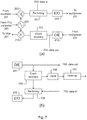
- Figure 7 shows only the additional elements to the frequency transfer system of Figure 2 needed for realizing the data transfer as well as neighboring elements to said additional elements.
- Figure 7(a) corresponds to the transmitter side and Figure 7(b) to the receiver side. It should be appreciated that similar additional elements may be added to any of the embodiments illustrated in Figure 3 to 6 to implement data transfer.
- the data transfer may be realized by the addition of two new elements to the transmitter of Figure 2 : a re-timing unit 701 and a clock recovery circuit 702.
- the re-timing unit 701 may re-time (synchronize) the clock frequency of the data stream to the reference frequency to be transmitted (that is, a corresponding mixing product of the RF mixer 202).
- the data stream may be provided as an input 703 of the re-timing unit 701.
- the RF filter 203 is not explicitly shown in Figure 7(a) , the RF filter 203 may be included in the transmitter as a separate element as in Figure 2 or it may be integrated into the re-timing unit 701.
- the reference frequency to be transmitted must match the requirements of the data stream and must be equal on average to the clock frequency of the data stream.
- the clock frequency of the received data stream (corresponding in this embodiment to the reference frequency) may be recovered from the received data stream using a clock recovery circuit 702.
- the recovered frequency possibly multiplied, divided, and/or filtered, may then be used to complete the phase-locked loop as in the previous embodiments.
- a data output 704 may be provided between the O/E converter 212 and the clock frequency unit 702. Referring to Figure 7(b) , the data transfer in the receiver may be realized in a similar but, in a sense, inverse manner compared to the transmitter.
- a clock recovery circuit 705 may be used to retrieve the clock frequency of the data stream, similar to the backward path of the transmitter. This frequency may then be used to re-time a data stream to be transmitted back to the transmitter using the re-timing unit 708. The recovered frequency may be filtered, multiplied, and/or divided by the element 706.
- a clean-up circuit 707 based on, for example, a low-noise oscillator in a phase-locked loop may also be used.
- a data output 709 may be provided after the O/E converter while a data input 710 may be integrated into the re-timing unit 708.
- time transfer in said time transfer system may be based on embedding time markers (that is, coding timing information) into the transferred signal.
- Said time markers may be, for example, specific bit patterns or amplitude, frequency, phase, or pulse width changes in the signal. Time transfer may be achieved with any of the previously described embodiments of the invention with a few modifications to the transmitter and the receiver.
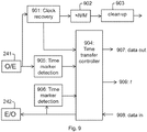
- FIG. 8 Additional elements needed for realizing time transfer for a transmitter according to Figure 2 are illustrated in Figure 8 and for a receiver according to Figure 2 in Figure 9 . Said additional elements provide means for coding as well as decoding timing information for the transmitter and the receiver. Apart from the new elements, the transmitter/receiver architecture may be the same as shown in Figure 2 or in any of Figures 3 to 6 .
- a time transfer controller 801 may be provided for applying time markers as described in the previous paragraph to the signal to be transmitted (the output signal of the RF mixer 202) based on a time reference 807.
- the timing information contained in the time markers may be used by the receiver for adjusting its internal clock.
- the time transfer controller 801 may also take as its input the received electrical signal (that is, the output signal of the O/E converter 212).
- Two time marker detection units 802, 803 may be arranged to detect the time markers applied to the input signal of the E/O converter 204 and the output signal of the O/E converter 212 and feed signals carrying said time-marker information back to the time transfer controller 801.
- a clock recovery circuit 804 may be provided in the backward path before the RF mixer 210.
- the time transfer controller 801 may also have a data input 805 and a data output 806 for inputting data to be transferred along with the time reference and for outputting data transferred from the receiver to the transmitter.
- one or both of the time marker detection units 802, 803 may be comprised in the time transfer controller 801.
- Figure 9 shows how similar elements as shown in Figure 8 may also be used for realizing the time transfer in the receiver.
- the output signal of the O/E converter 241 may be fed to a clock recovery circuit 901 to recover the transferred frequency which may be consequently multiplied, divided, filtered and/or cleaned up by elements 902, 903.
- the clock recovery circuit 901 may also provide an output to the time transfer controller 904 which may embed time markers to the electrical signal to be transmitted back to the transmitter and time stamp the time markers using an internal clock of the time transfer controller 904.
- the time transfer controller 904 may be provided with the time marker information of the transmitted electrical signal by the time marker detection unit 905 which takes as its input the output signal of the O/E converter 241.
- Another time marker recovery unit 906 may be provided to recover the time markers from the signal fed to the E/O converter 242 (that is, the electrical signal to be transmitted back to the transmitter).
- the internal clock may be phase-locked to the transmitted frequency reference signal (the output signal of the clock recovery circuit 901).
- the time transfer controller 904 may also have a data input 908 and a data output 907 for inputting data to be transferred along with the time reference and for outputting data transferred to the receiver from the transmitter. Similar to the transmitter of Figure 8 , one or both of the time marker detection units 905, 906 may be comprised in the time transfer controller 904 in some embodiments.
- the time transfer controller 801 of the transmitter in Figure 8 and the time transfer controller 904 of the receiver in Figure 9 may transmit the timing information between them using the data stream or possibly another channel. Based on the timing information, the time difference between the clock of the transmitter and the clock of the receiver may be computed, after which the clock of the receiver may be adjusted accordingly.
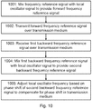
- Figure 10 shows a method according to an embodiment of the invention for realizing frequency transfer in a transmitter.
- the illustrated method may be, for example, performed by any of the transmitters according to embodiments of the invention illustrated in Figures 2 to 9 .
- the transmitter mixes, in block 1001, a frequency reference signal having a reference frequency with a local oscillator signal having a local oscillator frequency.
- One resulting mixing product represents a forward frequency reference signal.
- the transmitter transmits, in block 1002, the forward frequency reference signal over the transmission medium to the receiving end.
- the transmitter receives, in block 1003, a first backward frequency reference signal over the transmission medium from the receiving end.
- the first backward frequency reference signal may be formed by a portion of the forward frequency reference signal being reflected back from the receiving end or by replicating the forward frequency reference signal in the receiving end and transmitting the replicated forward frequency reference signal back from the receiving end.
- the transmitter mixes, in block 1004, the first backward frequency reference signal with the local oscillator signal.
- One resulting second mixing product represents a second backward frequency reference signal (having a second backward reference frequency).
- the transmitter adjusts, in block 1005, the local oscillator frequency based on a phase shift of the second backward frequency reference signal so as to compensate for a phase shift of the forward frequency reference signal that occurs in the transmission medium.
Landscapes
- Engineering & Computer Science (AREA)
- Physics & Mathematics (AREA)
- Computer Networks & Wireless Communication (AREA)
- Signal Processing (AREA)
- Electromagnetism (AREA)
- Theoretical Computer Science (AREA)
- General Engineering & Computer Science (AREA)
- General Physics & Mathematics (AREA)
- Optics & Photonics (AREA)
- Optical Communication System (AREA)
- Transmitters (AREA)
Claims (15)
- Vorrichtung zur Verteilung einer Frequenzreferenz über ein Übertragungsmedium (230) an ein Empfangsende (240), wobei die Vorrichtung Folgendes umfassteinen ersten Mischer (202, 302, 402, 502) vorzugsweise eines Aufwärtswandlungstyps, der angepasst ist, ein Frequenzreferenzsignal mit einer Referenzfrequenz mit einem lokalen Oszillatorsignal mit einer lokalen Oszillatorfrequenz zu mischen, wobei ein Mischprodukt des ersten Mischers (202, 302, 402, 502) ein Vorwärtsfrequenzreferenzsignal repräsentiert;einen Kommunikationsbereich (231, 230, 232), der angepasst ist, das Vorwärtsfrequenzreferenzsignal über das Übertragungsmedium (230) zum Empfangsende (240) zu übertragen, und angepasst ist, ein erstes Rückwärtsfrequenzreferenzsignal über das Übertragungsmedium (230) vom Empfangsende (240) zu empfangen, wobei das erste Rückwärtsfrequenzreferenzsignal durch einen Abschnitt des Vorwärtsfrequenzreferenzsignals, das vom Empfangsende (240) zurück reflektiert wird, oder durch Replizieren des Vorwärtsfrequenzreferenzsignals im Empfangsende (240) und Übertragen des replizierten Vorwärtsfrequenzreferenzsignals zurück vom Empfangsende (240) gebildet wird;einen zweiten Mischer (210, 310, 410, 510), der angepasst ist, das erste Rückwärtsfrequenzreferenzsignal mit dem lokalen Oszillatorsignal mit der lokalen Oszillatorfrequenz zu mischen, wobei ein Mischprodukt des zweiten Mischers (210, 310, 410, 510) ein zweites Rückwärtsfrequenzreferenzsignal repräsentiert; undeine Phasenkomparator- und Steuerschaltung (205, 208, 305, 308, 405, 408, 505, 508), die angepasst ist, die lokale Oszillatorfrequenz auf Basis einer Phasenverschiebung des zweiten Rückwärtsfrequenzreferenzsignals einzustellen, um eine Phasenverschiebung des Vorwärtsfrequenzreferenzsignals, die im Übertragungsmedium (230) auftritt, zu kompensieren.
- Vorrichtung nach Anspruch 1, wobei der erste Mischer und der zweiten Mischer Mischer desselben Typs sind.
- Vorrichtung nach Anspruch 1 oder 2, wobei die Phasenkomparator- und Steuerschaltung (205, 208, 305, 308, 405, 408, 505, 508) eine Phasenregelschleifensteuerung (205, 305, 405, 505) umfasst, die eine lokale Oszillatorfrequenz eines lokalen Oszillators (201, 301, 401, 501), der eine Phasenregelschleife ansteuert, steuert.
- Vorrichtung nach einem der vorhergehenden Ansprüche, wobei die Phasenkomparator- und Steuerschaltung (205, 208, 305, 308, 405, 408, 505, 508) einen Frequenzwandler (207, 307, 507) umfasst, der angepasst ist, eine der Referenzfrequenz und einer zweiten Rückwärtsreferenzfrequenz des zweiten Rückwärtsfrequenzreferenzsignals umzuwandeln, um die Frequenzen für einen Phasenvergleich abzugleichen, wobei der Frequenzwandler (207, 307, 507) vorzugsweise einen Frequenzvervielfacher und/oder einen Frequenzteiler umfasst.
- Vorrichtung nach einem der vorhergehenden Ansprüche, die ferner Folgendes umfasstMittel zum Codieren von Taktungsinformationen in das Vorwärtsfrequenzreferenzsignal, um eine Taktreferenz bereitzustellen; undMittel zum Decodieren von Taktungsinformationen aus dem ersten Rückwärtsfrequenzreferenzsignal.
- Vorrichtung nach einem der vorhergehenden Ansprüche, die ferner eines oder mehreres von Folgendem umfasst:ein erstes Bandpassfilter (203, 303, 403, 503), das angepasst ist, ein Ausgangssignal des ersten Mischers (202, 302, 402, 502) zu filtern, um nur das Mischprodukt des ersten Mischers als die Vorwärtsfrequenzreferenz zur Übertragung durchzulassen;ein zweites Bandpassfilter (211, 311, 411, 511), das angepasst ist, das erste Rückwärtsfrequenzreferenzsignal zu filtern, um nach Empfang nur das Mischprodukt des ersten Mischers (202, 302, 402, 502) durchzulassen; undein drittes Bandpassfilter (209, 309, 409, 509), das angepasst ist, ein Ausgangssignal des zweiten Mischers (210, 310, 410, 510) zu filtern, um nur das Mischprodukt des zweiten Mischers (210, 310, 410, 510) als das zweite Rückwärtsfrequenzreferenzsignal zur Phasenkomparator- und Steuerschaltung (205, 208, 305, 308, 405, 408, 505, 508) durchzulassen.
- Vorrichtung nach Anspruch 6, wobei das Mischprodukt des ersten Mischers (202, 302, 402, 502) und das Mischprodukt des zweiten Mischers (210, 310, 410, 510) Mischprodukte desselben Typs sind, wobei der Typ vorzugsweise einer Summe oder einer positiven Differenz zwischen Frequenzen von zu mischenden Signalen entspricht.
- Vorrichtung nach einem der vorhergehenden Ansprüche, wobei die Referenzfrequenz im Wesentlichen mit der lokalen Oszillatorfrequenz gleich oder ein Vielfaches derselben ist oder die lokale Oszillatorfrequenz im Wesentlichen ein Vielfaches der Referenzfrequenz ist.
- Vorrichtung nach einem der vorhergehenden Ansprüche, die ferner Folgendes umfasst:eine Umtaktungseinheit (703), die angepasst ist, einen ersten Datenstrom zu empfangen, eine erste Taktfrequenz des ersten Datenstroms mit einer Vorwärtsfrequenzreferenz des Vorwärtsfrequenzreferenzsignals umzutakten und einen umgetakteten ersten Datenstrom im Vorwärtsfrequenzreferenzsignal zu übertragen;einen Datenausgang (704) zum Ausgeben eines ersten Rückwärtsfrequenzreferenzdatensignals, wobei das erste Rückwärtsfrequenzreferenzdatensignal das erste Rückwärtsfrequenzreferenzsignal, das einen zweiten Datenstrom umfasst, ist; undeine Taktrückgewinnungsschaltung (702), die angepasst ist, ein erstes Rückwärtsfrequenzreferenzsignal aus dem ersten Rückwärtsfrequenzreferenzdatensignal rückzugewinnen.
- Vorrichtung nach einem der vorhergehenden Ansprüche, wobei die Referenzfrequenz und die lokale Oszillatorfrequenz Funkfrequenzen sind.
- Vorrichtung nach einem der vorhergehenden Ansprüche, wobei das Übertragungsmedium (230) ein optisches Übertragungsmedium umfasst, wobei die Vorrichtung ferner Folgendes umfasst:einen ersten Elektrisch-Optisch-Wandler (204, 304, 404), der angepasst ist, das Vorwärtsfrequenzreferenzsignal vor der Übertragung in ein optisches Vorwärtsfrequenzsignal umzuwandeln; undeinen ersten Optisch-Elektrisch-Wandler (212, 312, 412), der angepasst ist, ein optisches Rückwärtsfrequenzsignal nach Empfang in das Rückwärtsfrequenzreferenzsignal umzuwandeln.
- Vorrichtung nach einem der Ansprüche 1 bis 10, wobei das Übertragungsmedium geführte Funkübertragungsmedien und/oder ein Freiraumfunkübertragungsmedium umfasst.
- System, das Folgendes umfasst:eine Referenzfrequenzverteilungsvorrichtung (220) nach einem der vorhergehenden Ansprüche;einen Empfänger (240), der einen teilweisen Reflektor zum Reflektieren eines Abschnitts des Vorwärtsfrequenzreferenzsignals zurück zur Referenzfrequenzverteilungsvorrichtung umfasst; undein Übertragungsmedium (231), das die Referenzfrequenzverteilungsvorrichtung und den Empfänger verbindet.
- System nach Anspruch 13, wobei die Referenzfrequenzverteilungsvorrichtung eine Vorrichtung nach Anspruch 11 ist und der Empfänger ferner Folgendes umfasst:einen zweiten Optisch-Elektrisch-Wandler (241), der angepasst ist, das optische Vorwärtsfrequenzsignal nach Empfang in das Vorwärtsfrequenzreferenzsignal umzuwandeln; undeinen zweiten Elektrisch-Optisch-Wandler (242), der angepasst ist, das Rückwärtsfrequenzreferenzsignal vor der Übertragung in das optische Rückwärtsfrequenzsignal umzuwandeln,wobei das System ferner Folgendes umfasst:einen Sendermultiplexer (231) zum Verbinden des optischen Vorwärtsfrequenzsignals mit dem Lichtwellenleiter und der optischen Rückwärtsfrequenz vom Lichtwellenleiter mit dem ersten Optisch-Elektrisch-Wandler (212, 312, 412); undeinen Empfängermultiplexer (232) zum Verbinden des optischen Rückwärtsfrequenzsignals mit dem Lichtwellenleiter und des optischen Vorwärtsfrequenzsignal vom Lichtwellenleiter mit dem zweiten Optisch-Elektrisch-Wandler.
- Verfahren zur Verteilung einer Frequenzreferenz über ein Übertragungsmedium an ein Empfangsende, wobei das Verfahren Folgendes umfasst;Mischen (1001) eines Frequenzreferenzsignals mit einer Referenzfrequenz mit einem lokalen Oszillatorsignal mit einer lokalen Oszillatorfrequenz, um ein erstes Mischprodukt bereitzustellen, wobei das erste Mischprodukt ein Vorwärtsfrequenzreferenzsignal repräsentiert;Übertragen (1002) des Vorwärtsfrequenzreferenzsignals über das Übertragungsmedium zum Empfangsende;Empfangen (1003) eines ersten Rückwärtsfrequenzreferenzsignals über das Übertragungsmedium vom Empfangsende, wobei das erste Rückwärtsfrequenzreferenzsignal durch einen Abschnitt des Vorwärtsfrequenzreferenzsignals, das vom Empfangsende zurück reflektiert wird, oder durch Replizieren des Vorwärtsfrequenzreferenzsignals im Empfangsende und Übertragen des replizierten Vorwärtsfrequenzreferenzsignals zurück vom Empfangsende gebildet wird;Mischen (1004) des ersten Rückwärtsfrequenzreferenzsignals mit dem lokalen Oszillatorsignal, um ein zweites Mischprodukt bereitzustellen, wobei das zweite Mischprodukt ein zweites Rückwärtsfrequenzreferenzsignal repräsentiert; undEinstellen (1005) der lokalen Oszillatorfrequenz auf Basis einer Phasenverschiebung eines zweiten Rückwärtsfrequenzreferenzsignals, um eine Phasenverschiebung des Vorwärtsfrequenzreferenzsignals, die im Übertragungsmedium auftritt, zu kompensieren.
Applications Claiming Priority (2)
| Application Number | Priority Date | Filing Date | Title |
|---|---|---|---|
| FI20175838A FI129033B (en) | 2017-09-21 | 2017-09-21 | Transmission of radio frequency and time over long distances |
| PCT/FI2018/050679 WO2019058028A1 (en) | 2017-09-21 | 2018-09-20 | FREQUENCY AND RF TIME TRANSFER AT LONG DISTANCE |
Publications (2)
| Publication Number | Publication Date |
|---|---|
| EP3685529A1 EP3685529A1 (de) | 2020-07-29 |
| EP3685529B1 true EP3685529B1 (de) | 2021-11-10 |
Family
ID=63915062
Family Applications (1)
| Application Number | Title | Priority Date | Filing Date |
|---|---|---|---|
| EP18789459.7A Not-in-force EP3685529B1 (de) | 2017-09-21 | 2018-09-20 | Langstrecken-hf-frequenz und -zeitübertragung |
Country Status (4)
| Country | Link |
|---|---|
| US (1) | US10911145B2 (de) |
| EP (1) | EP3685529B1 (de) |
| FI (1) | FI129033B (de) |
| WO (1) | WO2019058028A1 (de) |
Families Citing this family (13)
| Publication number | Priority date | Publication date | Assignee | Title |
|---|---|---|---|---|
| US10735097B2 (en) * | 2017-11-21 | 2020-08-04 | Cable Television Laboratories, Inc | Systems and methods for full duplex coherent optics |
| US10917175B2 (en) | 2017-11-21 | 2021-02-09 | Cable Television Laboratories, Inc. | Systems and methods for full duplex coherent optics |
| CN111147149B (zh) * | 2019-12-17 | 2022-09-02 | 上海交通大学 | 基于被动相位补偿的光学频率传递装置与传递方法 |
| CN111147150B (zh) * | 2019-12-18 | 2023-02-07 | 上海交通大学 | 基于被动相位补偿的分布式光学频率传递装置与传递方法 |
| CN111698032B (zh) * | 2020-06-16 | 2021-04-20 | 中国科学院国家授时中心 | 一种单纤单向时间传递方法及系统 |
| CN113098622B (zh) * | 2021-03-14 | 2022-01-28 | 北京邮电大学 | 一种基于光学频率梳双向相位抖动补偿的频率传递装置 |
| CN113179395B (zh) * | 2021-04-30 | 2021-10-15 | 深圳市金乾象科技有限公司 | 一种摄像头远程监控视频传输装置 |
| CN113179394A (zh) * | 2021-04-30 | 2021-07-27 | 深圳市金乾象科技有限公司 | 一种远程视频监控装置 |
| CN113259864B (zh) * | 2021-06-29 | 2021-09-21 | 广州慧睿思通科技股份有限公司 | 窄带通信方法、对讲机、设备、存储介质及自组网系统 |
| CN114629554B (zh) * | 2022-03-15 | 2023-06-20 | 中国科学院精密测量科学与技术创新研究院 | 一种频率参考信号传递系统及方法 |
| US12439351B2 (en) * | 2022-05-11 | 2025-10-07 | Hughes Network Systems, Llc | Communication systems and methods for synchronizing clock timing and frequency |
| CN116599591A (zh) * | 2023-04-03 | 2023-08-15 | 北京邮电大学 | 射频参考信号的传递系统及传递方法 |
| CN118802093B (zh) * | 2024-04-28 | 2025-10-24 | 清华大学 | 频率传输系统及方法 |
Family Cites Families (3)
| Publication number | Priority date | Publication date | Assignee | Title |
|---|---|---|---|---|
| US5031234A (en) * | 1989-05-31 | 1991-07-09 | The United States Of America As Represented By The Administrator Of The National Aeronautics And Space Administration | Fiber optic frequency transfer link |
| JPH04283680A (ja) * | 1991-03-12 | 1992-10-08 | Stanley Electric Co Ltd | 光波測距装置 |
| US20150248047A1 (en) * | 2014-02-28 | 2015-09-03 | The University Of Manchester | Terahertz Mixer and Optical Fiber Coupled Terahertz Mixer |
-
2017
- 2017-09-21 FI FI20175838A patent/FI129033B/en active IP Right Grant
-
2018
- 2018-09-20 WO PCT/FI2018/050679 patent/WO2019058028A1/en not_active Ceased
- 2018-09-20 EP EP18789459.7A patent/EP3685529B1/de not_active Not-in-force
- 2018-09-20 US US16/648,418 patent/US10911145B2/en active Active
Also Published As
| Publication number | Publication date |
|---|---|
| FI129033B (en) | 2021-05-31 |
| US10911145B2 (en) | 2021-02-02 |
| EP3685529A1 (de) | 2020-07-29 |
| US20200266895A1 (en) | 2020-08-20 |
| WO2019058028A1 (en) | 2019-03-28 |
| FI20175838A1 (en) | 2019-03-22 |
Similar Documents
| Publication | Publication Date | Title |
|---|---|---|
| EP3685529B1 (de) | Langstrecken-hf-frequenz und -zeitübertragung | |
| JP6821099B2 (ja) | 光伝送装置及び光伝送システム | |
| CN109039469B (zh) | 时频标准信号融合传输系统及传输方法 | |
| EP2939353B1 (de) | Optoelektronischer pll-oszillator mit selbstinjektion | |
| KR101651496B1 (ko) | 밀리미터파 대역 무선 송수신 장치 | |
| JP2020092412A (ja) | アクティブアンテナシステム | |
| KR101247177B1 (ko) | 코히어런트 네트워크 mimo를 위한 안테나 동기화 | |
| Devgan | A review of optoelectronic oscillators for high speed signal processing applications | |
| CN111416667A (zh) | 一种宽带信道化接收机 | |
| CN106301576B (zh) | 一种基于无源相位校正的多频率多点微波光纤稳相传输方法 | |
| Bai et al. | Microwave photonic links and transversal microwave photonic applications | |
| Rani et al. | Photonic generation of frequency 12‐tupling millimeter‐wave based on three cascaded‐MZMs and polarization multiplexing | |
| Seeds | Optical technologies for phased array antennas | |
| CN115189776B (zh) | 射频信号的被动稳相光载传输方法及系统 | |
| Sun et al. | Frequency synthesis of forced opto-electronic oscillators at the X-band | |
| WO2017050053A1 (zh) | 光发射装置、发射方法、光接收装置及接收方法 | |
| Lin et al. | Multifunctional fronthaul architecture enabled by electro-optic comb cloning | |
| CN110601762A (zh) | 一种实现相位噪声补偿的射频信号传输方法及传输系统 | |
| Ghelfi et al. | Novel architecture for a photonics-assisted radar transceiver based on a single mode-locking laser | |
| US20240369905A1 (en) | Transfer of signals between the radio frequency and terahertz frequency domains | |
| Minoofar et al. | High-capacity THz communications using multiple orbital-angular-momentum beams | |
| Bai et al. | Fiber-based multiple-access ultrastable radio and optical frequency dissemination | |
| US20250038854A1 (en) | Dual laser control for point-to-multipoint networks using bi-directional transmission | |
| JP3974255B2 (ja) | 周波数可変レーザ光源装置 | |
| Rodwell et al. | Optical phase-locking and wavelength synthesis |
Legal Events
| Date | Code | Title | Description |
|---|---|---|---|
| STAA | Information on the status of an ep patent application or granted ep patent |
Free format text: STATUS: UNKNOWN |
|
| STAA | Information on the status of an ep patent application or granted ep patent |
Free format text: STATUS: THE INTERNATIONAL PUBLICATION HAS BEEN MADE |
|
| PUAI | Public reference made under article 153(3) epc to a published international application that has entered the european phase |
Free format text: ORIGINAL CODE: 0009012 |
|
| STAA | Information on the status of an ep patent application or granted ep patent |
Free format text: STATUS: REQUEST FOR EXAMINATION WAS MADE |
|
| 17P | Request for examination filed |
Effective date: 20200416 |
|
| AK | Designated contracting states |
Kind code of ref document: A1 Designated state(s): AL AT BE BG CH CY CZ DE DK EE ES FI FR GB GR HR HU IE IS IT LI LT LU LV MC MK MT NL NO PL PT RO RS SE SI SK SM TR |
|
| AX | Request for extension of the european patent |
Extension state: BA ME |
|
| DAV | Request for validation of the european patent (deleted) | ||
| DAX | Request for extension of the european patent (deleted) | ||
| GRAP | Despatch of communication of intention to grant a patent |
Free format text: ORIGINAL CODE: EPIDOSNIGR1 |
|
| STAA | Information on the status of an ep patent application or granted ep patent |
Free format text: STATUS: GRANT OF PATENT IS INTENDED |
|
| INTG | Intention to grant announced |
Effective date: 20210611 |
|
| RAP3 | Party data changed (applicant data changed or rights of an application transferred) |
Owner name: TEKNOLOGIAN TUTKIMUSKESKUS VTT OY |
|
| RAP3 | Party data changed (applicant data changed or rights of an application transferred) |
Owner name: TEKNOLOGIAN TUTKIMUSKESKUS VTT OY |
|
| GRAS | Grant fee paid |
Free format text: ORIGINAL CODE: EPIDOSNIGR3 |
|
| GRAA | (expected) grant |
Free format text: ORIGINAL CODE: 0009210 |
|
| STAA | Information on the status of an ep patent application or granted ep patent |
Free format text: STATUS: THE PATENT HAS BEEN GRANTED |
|
| AK | Designated contracting states |
Kind code of ref document: B1 Designated state(s): AL AT BE BG CH CY CZ DE DK EE ES FI FR GB GR HR HU IE IS IT LI LT LU LV MC MK MT NL NO PL PT RO RS SE SI SK SM TR |
|
| REG | Reference to a national code |
Ref country code: GB Ref legal event code: FG4D |
|
| REG | Reference to a national code |
Ref country code: AT Ref legal event code: REF Ref document number: 1447044 Country of ref document: AT Kind code of ref document: T Effective date: 20211115 Ref country code: CH Ref legal event code: EP |
|
| REG | Reference to a national code |
Ref country code: DE Ref legal event code: R096 Ref document number: 602018026580 Country of ref document: DE |
|
| REG | Reference to a national code |
Ref country code: IE Ref legal event code: FG4D |
|
| REG | Reference to a national code |
Ref country code: LT Ref legal event code: MG9D |
|
| REG | Reference to a national code |
Ref country code: NL Ref legal event code: MP Effective date: 20211110 |
|
| REG | Reference to a national code |
Ref country code: AT Ref legal event code: MK05 Ref document number: 1447044 Country of ref document: AT Kind code of ref document: T Effective date: 20211110 |
|
| PG25 | Lapsed in a contracting state [announced via postgrant information from national office to epo] |
Ref country code: RS Free format text: LAPSE BECAUSE OF FAILURE TO SUBMIT A TRANSLATION OF THE DESCRIPTION OR TO PAY THE FEE WITHIN THE PRESCRIBED TIME-LIMIT Effective date: 20211110 Ref country code: LT Free format text: LAPSE BECAUSE OF FAILURE TO SUBMIT A TRANSLATION OF THE DESCRIPTION OR TO PAY THE FEE WITHIN THE PRESCRIBED TIME-LIMIT Effective date: 20211110 Ref country code: FI Free format text: LAPSE BECAUSE OF FAILURE TO SUBMIT A TRANSLATION OF THE DESCRIPTION OR TO PAY THE FEE WITHIN THE PRESCRIBED TIME-LIMIT Effective date: 20211110 Ref country code: BG Free format text: LAPSE BECAUSE OF FAILURE TO SUBMIT A TRANSLATION OF THE DESCRIPTION OR TO PAY THE FEE WITHIN THE PRESCRIBED TIME-LIMIT Effective date: 20220210 Ref country code: AT Free format text: LAPSE BECAUSE OF FAILURE TO SUBMIT A TRANSLATION OF THE DESCRIPTION OR TO PAY THE FEE WITHIN THE PRESCRIBED TIME-LIMIT Effective date: 20211110 |
|
| PG25 | Lapsed in a contracting state [announced via postgrant information from national office to epo] |
Ref country code: IS Free format text: LAPSE BECAUSE OF FAILURE TO SUBMIT A TRANSLATION OF THE DESCRIPTION OR TO PAY THE FEE WITHIN THE PRESCRIBED TIME-LIMIT Effective date: 20220310 Ref country code: SE Free format text: LAPSE BECAUSE OF FAILURE TO SUBMIT A TRANSLATION OF THE DESCRIPTION OR TO PAY THE FEE WITHIN THE PRESCRIBED TIME-LIMIT Effective date: 20211110 Ref country code: PT Free format text: LAPSE BECAUSE OF FAILURE TO SUBMIT A TRANSLATION OF THE DESCRIPTION OR TO PAY THE FEE WITHIN THE PRESCRIBED TIME-LIMIT Effective date: 20220310 Ref country code: PL Free format text: LAPSE BECAUSE OF FAILURE TO SUBMIT A TRANSLATION OF THE DESCRIPTION OR TO PAY THE FEE WITHIN THE PRESCRIBED TIME-LIMIT Effective date: 20211110 Ref country code: NO Free format text: LAPSE BECAUSE OF FAILURE TO SUBMIT A TRANSLATION OF THE DESCRIPTION OR TO PAY THE FEE WITHIN THE PRESCRIBED TIME-LIMIT Effective date: 20220210 Ref country code: NL Free format text: LAPSE BECAUSE OF FAILURE TO SUBMIT A TRANSLATION OF THE DESCRIPTION OR TO PAY THE FEE WITHIN THE PRESCRIBED TIME-LIMIT Effective date: 20211110 Ref country code: LV Free format text: LAPSE BECAUSE OF FAILURE TO SUBMIT A TRANSLATION OF THE DESCRIPTION OR TO PAY THE FEE WITHIN THE PRESCRIBED TIME-LIMIT Effective date: 20211110 Ref country code: HR Free format text: LAPSE BECAUSE OF FAILURE TO SUBMIT A TRANSLATION OF THE DESCRIPTION OR TO PAY THE FEE WITHIN THE PRESCRIBED TIME-LIMIT Effective date: 20211110 Ref country code: GR Free format text: LAPSE BECAUSE OF FAILURE TO SUBMIT A TRANSLATION OF THE DESCRIPTION OR TO PAY THE FEE WITHIN THE PRESCRIBED TIME-LIMIT Effective date: 20220211 Ref country code: ES Free format text: LAPSE BECAUSE OF FAILURE TO SUBMIT A TRANSLATION OF THE DESCRIPTION OR TO PAY THE FEE WITHIN THE PRESCRIBED TIME-LIMIT Effective date: 20211110 |
|
| PG25 | Lapsed in a contracting state [announced via postgrant information from national office to epo] |
Ref country code: SM Free format text: LAPSE BECAUSE OF FAILURE TO SUBMIT A TRANSLATION OF THE DESCRIPTION OR TO PAY THE FEE WITHIN THE PRESCRIBED TIME-LIMIT Effective date: 20211110 Ref country code: SK Free format text: LAPSE BECAUSE OF FAILURE TO SUBMIT A TRANSLATION OF THE DESCRIPTION OR TO PAY THE FEE WITHIN THE PRESCRIBED TIME-LIMIT Effective date: 20211110 Ref country code: RO Free format text: LAPSE BECAUSE OF FAILURE TO SUBMIT A TRANSLATION OF THE DESCRIPTION OR TO PAY THE FEE WITHIN THE PRESCRIBED TIME-LIMIT Effective date: 20211110 Ref country code: EE Free format text: LAPSE BECAUSE OF FAILURE TO SUBMIT A TRANSLATION OF THE DESCRIPTION OR TO PAY THE FEE WITHIN THE PRESCRIBED TIME-LIMIT Effective date: 20211110 Ref country code: DK Free format text: LAPSE BECAUSE OF FAILURE TO SUBMIT A TRANSLATION OF THE DESCRIPTION OR TO PAY THE FEE WITHIN THE PRESCRIBED TIME-LIMIT Effective date: 20211110 Ref country code: CZ Free format text: LAPSE BECAUSE OF FAILURE TO SUBMIT A TRANSLATION OF THE DESCRIPTION OR TO PAY THE FEE WITHIN THE PRESCRIBED TIME-LIMIT Effective date: 20211110 |
|
| REG | Reference to a national code |
Ref country code: DE Ref legal event code: R097 Ref document number: 602018026580 Country of ref document: DE |
|
| PLBE | No opposition filed within time limit |
Free format text: ORIGINAL CODE: 0009261 |
|
| STAA | Information on the status of an ep patent application or granted ep patent |
Free format text: STATUS: NO OPPOSITION FILED WITHIN TIME LIMIT |
|
| 26N | No opposition filed |
Effective date: 20220811 |
|
| PG25 | Lapsed in a contracting state [announced via postgrant information from national office to epo] |
Ref country code: AL Free format text: LAPSE BECAUSE OF FAILURE TO SUBMIT A TRANSLATION OF THE DESCRIPTION OR TO PAY THE FEE WITHIN THE PRESCRIBED TIME-LIMIT Effective date: 20211110 |
|
| PG25 | Lapsed in a contracting state [announced via postgrant information from national office to epo] |
Ref country code: SI Free format text: LAPSE BECAUSE OF FAILURE TO SUBMIT A TRANSLATION OF THE DESCRIPTION OR TO PAY THE FEE WITHIN THE PRESCRIBED TIME-LIMIT Effective date: 20211110 |
|
| REG | Reference to a national code |
Ref country code: DE Ref legal event code: R119 Ref document number: 602018026580 Country of ref document: DE |
|
| PG25 | Lapsed in a contracting state [announced via postgrant information from national office to epo] |
Ref country code: MC Free format text: LAPSE BECAUSE OF FAILURE TO SUBMIT A TRANSLATION OF THE DESCRIPTION OR TO PAY THE FEE WITHIN THE PRESCRIBED TIME-LIMIT Effective date: 20211110 |
|
| REG | Reference to a national code |
Ref country code: CH Ref legal event code: PL |
|
| GBPC | Gb: european patent ceased through non-payment of renewal fee |
Effective date: 20220920 |
|
| REG | Reference to a national code |
Ref country code: BE Ref legal event code: MM Effective date: 20220930 |
|
| PG25 | Lapsed in a contracting state [announced via postgrant information from national office to epo] |
Ref country code: IT Free format text: LAPSE BECAUSE OF FAILURE TO SUBMIT A TRANSLATION OF THE DESCRIPTION OR TO PAY THE FEE WITHIN THE PRESCRIBED TIME-LIMIT Effective date: 20211110 |
|
| PG25 | Lapsed in a contracting state [announced via postgrant information from national office to epo] |
Ref country code: LU Free format text: LAPSE BECAUSE OF NON-PAYMENT OF DUE FEES Effective date: 20220920 |
|
| PG25 | Lapsed in a contracting state [announced via postgrant information from national office to epo] |
Ref country code: LI Free format text: LAPSE BECAUSE OF NON-PAYMENT OF DUE FEES Effective date: 20220930 Ref country code: IE Free format text: LAPSE BECAUSE OF NON-PAYMENT OF DUE FEES Effective date: 20220920 Ref country code: FR Free format text: LAPSE BECAUSE OF NON-PAYMENT OF DUE FEES Effective date: 20220930 Ref country code: DE Free format text: LAPSE BECAUSE OF NON-PAYMENT OF DUE FEES Effective date: 20230401 Ref country code: CH Free format text: LAPSE BECAUSE OF NON-PAYMENT OF DUE FEES Effective date: 20220930 |
|
| PG25 | Lapsed in a contracting state [announced via postgrant information from national office to epo] |
Ref country code: BE Free format text: LAPSE BECAUSE OF NON-PAYMENT OF DUE FEES Effective date: 20220930 |
|
| PG25 | Lapsed in a contracting state [announced via postgrant information from national office to epo] |
Ref country code: GB Free format text: LAPSE BECAUSE OF NON-PAYMENT OF DUE FEES Effective date: 20220920 |
|
| PG25 | Lapsed in a contracting state [announced via postgrant information from national office to epo] |
Ref country code: CY Free format text: LAPSE BECAUSE OF FAILURE TO SUBMIT A TRANSLATION OF THE DESCRIPTION OR TO PAY THE FEE WITHIN THE PRESCRIBED TIME-LIMIT Effective date: 20211110 |
|
| PG25 | Lapsed in a contracting state [announced via postgrant information from national office to epo] |
Ref country code: MK Free format text: LAPSE BECAUSE OF FAILURE TO SUBMIT A TRANSLATION OF THE DESCRIPTION OR TO PAY THE FEE WITHIN THE PRESCRIBED TIME-LIMIT Effective date: 20211110 Ref country code: HU Free format text: LAPSE BECAUSE OF FAILURE TO SUBMIT A TRANSLATION OF THE DESCRIPTION OR TO PAY THE FEE WITHIN THE PRESCRIBED TIME-LIMIT; INVALID AB INITIO Effective date: 20180920 |
|
| PG25 | Lapsed in a contracting state [announced via postgrant information from national office to epo] |
Ref country code: TR Free format text: LAPSE BECAUSE OF FAILURE TO SUBMIT A TRANSLATION OF THE DESCRIPTION OR TO PAY THE FEE WITHIN THE PRESCRIBED TIME-LIMIT Effective date: 20211110 |
|
| PG25 | Lapsed in a contracting state [announced via postgrant information from national office to epo] |
Ref country code: MT Free format text: LAPSE BECAUSE OF FAILURE TO SUBMIT A TRANSLATION OF THE DESCRIPTION OR TO PAY THE FEE WITHIN THE PRESCRIBED TIME-LIMIT Effective date: 20211110 |